JP4008654B2 - Thin film magnetic head and manufacturing method thereof - Google Patents
Thin film magnetic head and manufacturing method thereof Download PDFInfo
- Publication number
- JP4008654B2 JP4008654B2 JP2000363659A JP2000363659A JP4008654B2 JP 4008654 B2 JP4008654 B2 JP 4008654B2 JP 2000363659 A JP2000363659 A JP 2000363659A JP 2000363659 A JP2000363659 A JP 2000363659A JP 4008654 B2 JP4008654 B2 JP 4008654B2
- Authority
- JP
- Japan
- Prior art keywords
- thin film
- magnetic pole
- coil
- magnetic head
- coil parts
- Prior art date
- Legal status (The legal status is an assumption and is not a legal conclusion. Google has not performed a legal analysis and makes no representation as to the accuracy of the status listed.)
- Expired - Fee Related
Links
Images


Classifications
-
- G—PHYSICS
- G11—INFORMATION STORAGE
- G11B—INFORMATION STORAGE BASED ON RELATIVE MOVEMENT BETWEEN RECORD CARRIER AND TRANSDUCER
- G11B5/00—Recording by magnetisation or demagnetisation of a record carrier; Reproducing by magnetic means; Record carriers therefor
- G11B5/127—Structure or manufacture of heads, e.g. inductive
- G11B5/31—Structure or manufacture of heads, e.g. inductive using thin films
- G11B5/3109—Details
- G11B5/313—Disposition of layers
-
- G—PHYSICS
- G11—INFORMATION STORAGE
- G11B—INFORMATION STORAGE BASED ON RELATIVE MOVEMENT BETWEEN RECORD CARRIER AND TRANSDUCER
- G11B5/00—Recording by magnetisation or demagnetisation of a record carrier; Reproducing by magnetic means; Record carriers therefor
- G11B5/127—Structure or manufacture of heads, e.g. inductive
- G11B5/31—Structure or manufacture of heads, e.g. inductive using thin films
- G11B5/3163—Fabrication methods or processes specially adapted for a particular head structure, e.g. using base layers for electroplating, using functional layers for masking, using energy or particle beams for shaping the structure or modifying the properties of the basic layers
-
- G—PHYSICS
- G11—INFORMATION STORAGE
- G11B—INFORMATION STORAGE BASED ON RELATIVE MOVEMENT BETWEEN RECORD CARRIER AND TRANSDUCER
- G11B5/00—Recording by magnetisation or demagnetisation of a record carrier; Reproducing by magnetic means; Record carriers therefor
- G11B5/127—Structure or manufacture of heads, e.g. inductive
- G11B5/33—Structure or manufacture of flux-sensitive heads, i.e. for reproduction only; Combination of such heads with means for recording or erasing only
- G11B5/39—Structure or manufacture of flux-sensitive heads, i.e. for reproduction only; Combination of such heads with means for recording or erasing only using magneto-resistive devices or effects
- G11B5/3903—Structure or manufacture of flux-sensitive heads, i.e. for reproduction only; Combination of such heads with means for recording or erasing only using magneto-resistive devices or effects using magnetic thin film layers or their effects, the films being part of integrated structures
- G11B5/3967—Composite structural arrangements of transducers, e.g. inductive write and magnetoresistive read
Landscapes
- Engineering & Computer Science (AREA)
- Manufacturing & Machinery (AREA)
- Magnetic Heads (AREA)
Description
【0001】
【発明の属する技術分野】
本発明は、少なくとも書き込み用の誘導型磁気変換素子を有する薄膜磁気ヘッドおよびその製造方法に関する。
【0002】
【従来の技術】
近年、ハードディスク装置の面記録密度の向上に伴って、薄膜磁気ヘッドの性能向上が求められている。薄膜磁気ヘッドとしては、例えば、書き込み用の誘導型磁気変換素子を有する記録ヘッドと、読み出し用の磁気抵抗(以下、MR(Magneto Resistive )と記す。)素子を有する再生ヘッドとを積層した構造を有する複合型薄膜磁気ヘッドが広く用いられている。
【0003】
記録ヘッドは、例えば、記録ギャップ(write gap)を挟んでその上下に配設され、一端部において磁気的に連結された上部磁極(トップポール)および下部磁極(ボトムポール)と、磁束発生用のコイルとを含んで構成されている。上部磁極および下部磁極は、磁気記録媒体(以下、単に「記録媒体」という。)に面する記録媒体対向面(エアベアリング面)に近い側の領域の記録ギャップ近傍において互いに同一の一定幅(一定幅部分)を有しており、これらの部位により記録トラック幅を規定する「磁極部分」が構成されている。
【0004】
コイルの構造としては、例えば、上部磁極や下部磁極または上部磁極と下部磁極との接続部を中心として2次元的に(一平面内に)巻かれた「スパイラル構造」や、上部磁極や下部磁極の周囲を巻回する「ヘリカル構造」などが知られている。これらのコイル構造を適用した例として、例えば、特開平5−242429では、対向配置された上部磁性コアおよび下部磁性コアを備える薄膜磁気ヘッドにおいて、下部縞状導電膜および上部縞状導電膜等により構成されたヘリカル状導体コイルが上部磁性コアの周囲を巻回する構造を開示している。また、実用新案第3033043号では、対向配置された第1コアおよび第2コアを備える薄膜磁気ヘッドにおいて、第1コアの周囲を右回り(または左回り)に巻回すると共に第2コアの周囲を左回り(または右回り)に巻回する複数のスパイラル状の薄膜コイル層が階層的に配設され、これらの薄膜コイル層が互いに連結された構造を開示している。また、特開平5−101337では、対向配置された下層薄膜磁気コアおよび上層薄膜磁気コアを備える薄膜磁気ヘッドにおいて、下層薄膜磁気コアの周囲を巻回するヘリカル状コイルと上層薄膜磁気コアの周囲を巻回するヘリカル状コイルとがスパイラル状コイルを介して連結された構造を開示している。
【0005】
薄膜磁気ヘッドでは、例えば、情報の記録動作時においてコイルに電流が流れると、これに応じて磁束が発生する。このとき発生した磁束は、上部磁極および下部磁極により構成された磁束の伝播経路(以下、「磁路」という。)を経由し、磁極部分の一部を構成する上部磁極の一定幅部分へ伝播する。一定幅部分へ伝播した磁束は、さらに、そのエアベアリング面側の先端部に到達する。一定幅部分の先端部に到達した磁束が記録ギャップ近傍の外部に漏れることにより記録用の信号磁界が発生する。この信号磁界により記録媒体が部分的に磁化され、情報が記録される。
【0006】
【発明が解決しようとする課題】
ところで、近年、薄膜磁気ヘッドの小型化を目的として、例えば、コイルの小型化が求められている。コイルの小型化を考慮した際、2次元的な広がりを有するスパイラル構造よりも、コイルの占める領域が小さいヘリカル構造がコイル構造として適切であり、コイルの巻線間を緊密にすることによりコイル構造をより小型化することが可能であると考えられる。
【0007】
しかしながら、従来は、以下のような理由により、薄膜磁気ヘッドの製造に長時間を要すると共に、製造歩留りが低下するという問題があった。すなわち、例えば、コイルを小型化すべくコイルの巻線間を緊密にするためには、高い形成精度が要求される。このような場合には、高い形成精度を確保するためにコイルの製造工程が煩雑化するため、薄膜磁気ヘッドの製造に要する時間が長くなる。また、コイルの形成精度が十分でなかったり、コイル形成時において形成精度に微妙なずれが生じると、コイル巻線間の接触に起因して短絡等が生じ、薄膜磁気ヘッドの製造歩留りが低下する可能性がある。すなわち、従来は、コイルの小型化と製造歩留り等の向上とを適正に両立させることは困難であった。
【0008】
なお、上記の問題は、薄膜磁気ヘッドの他、これと同様の構造(対向する2つの磁性体と磁束発生用のコイル)を有する他の磁気ヘッド(例えばビデオテープ記録再生用のヘッド)においても同様に生じるものである。
【0009】
本発明はかかる問題点に鑑みてなされたもので、その目的は、コイルを小型化しつつ、製造時間を短縮すると共に製造歩留りを向上させることが可能な薄膜磁気ヘッドおよびその製造方法を提供することにある。
【0010】
【課題を解決するための手段】
本発明の薄膜磁気ヘッドは、記録媒体に面する記録媒体対向面からこの面と離れる方向に、膜厚方向において互いに対向するように延在し、記録媒体対向面に近い側の端部においてギャップ層を介して互いに対向すると共に記録媒体対向面から遠い側の端部において互いに磁気的に連結された下部磁極および上部磁極と、下部磁極を中心として所定の方向に巻回する複数の第1の巻回単位と上部磁極を中心として所定の方向と反対方向に巻回する複数の第2の巻回単位とを含み、下部磁極および上部磁極の延在方向に沿って延在する薄膜コイルと、薄膜コイルを下部磁極および上部磁極から絶縁する絶縁層とを有する薄膜磁気ヘッドであり、下部磁極および上部磁極が、ギャップ層を介して互いに対向する部分と互いに磁気的に連結される部分とを結ぶ直線上に沿って延在し、薄膜コイルが、記録媒体対向面から見て8の字を描くと共に各第1の巻回単位同士および各第2の巻回単位同士が重ならないよう第1の巻回単位と第2の巻回単位とを交互に連結してなる連続体をなし、第1の巻回単位の数と第2の巻回単位の数とが互いに一致するようにしたものである。
【0011】
本発明の薄膜磁気ヘッドでは、下部磁極および前記上部磁極が、ギャップ層を介して互いに対向する部分と互いに磁気的に連結される部分とを結ぶ直線上に沿って延在している場合に、薄膜コイルが、記録媒体対向面から見て8の字を描くと共に各第1の巻回単位同士および各第2の巻回単位同士が互いに重ならないよう第1の巻回単位と第2の巻回単位とを交互に連結してなる連続体をなし、第1の巻回単位の数と第2の巻回単位の数とが互いに一致している。これにより、薄膜コイルのうち、高い形成精度を要する部分の割合が減少する。また、下部磁極および上部磁極のそれぞれの周辺領域における磁束の発生量および発生タイミングが均等化する。
【0012】
本発明の薄膜磁気ヘッドでは、薄膜コイルが、下部磁極の下方の階層に配列された複数の帯状の第1のコイルパーツと、下部磁極と上部磁極との間の階層に配列された複数の帯状の第2のコイルパーツと、上部磁極の上方の階層に配列された複数の帯状の第3のコイルパーツと、第1および第2のコイルパーツの端部同士を接続させる複数の柱状の第4のコイルパーツと、第2および第3のコイルパーツの端部同士を接続させる複数の柱状の第5のコイルパーツとを含むようにしてもよい。この場合には、第1ないし第5のコイルパーツが別体形成されており、第2のコイルパーツが記録トラック幅方向に沿って延在し、第1および第3のコイルパーツが記録トラック幅方向に対して傾いて延在するようにしてもよいし、あるいは第1のコイルパーツが第2ないし第5のコイルパーツと別体形成されていると共に、第2および第4のコイルパーツが一体形成され、第3および第5のコイルパーツが一体形成されており、一体形成された第2および第4のコイルパーツが記録トラック幅方向に延在し、第1のコイルパーツならびに一体形成された第3および第5のコイルパーツが記録トラック幅方向に対して傾いて延在するようにしてもよい。また、下部磁極および上部磁極が、記録媒体対向面に近い側から順に、記録トラック幅を規定する一定幅を有する部分とそれよりも大きな幅を有する部分とを含むようにしてもよい。
【0013】
本発明の薄膜磁気ヘッドの製造方法は、記録媒体に面する記録媒体対向面からこの面と離れる方向に、膜厚方向において互いに対向するように延在し、記録媒体対向面に近い側の端部においてギャップ層を介して互いに対向すると共に記録媒体対向面から遠い側の端部において互いに磁気的に連結された下部磁極および上部磁極と、下部磁極を中心として所定の方向に巻回する複数の第1の巻回単位と上部磁極を中心として所定の方向と反対方向に巻回する複数の第2の巻回単位とを含み、下部磁極および上部磁極の延在方向に沿って延在する薄膜コイルと、薄膜コイルを下部磁極および上部磁極から絶縁する絶縁層とを有する薄膜磁気ヘッドの製造方法であり、ギャップ層を介して互いに対向する部分と互いに磁気的に連結される部分とを結ぶ直線上に沿って延在するように下部磁極および上部磁極を形成し、薄膜コイルを構成する複数の構成要素を順に積層して形成することにより、記録媒体対向面から見て8の字を描くと共に各第1の巻回単位同士および各第2の巻回単位同士が互いに重ならないように第1の巻回単位と第2の巻回単位とが交互に連結された連続体をなすように薄膜コイルを形成し、第1の巻回単位の数と第2の巻回単位の数とが互いに一致するようにしたものである。
【0014】
本発明の薄膜磁気ヘッドの製造方法では、ギャップ層を介して互いに対向する部分と互いに磁気的に連結される部分とを結ぶ直線上に沿って延在するように下部磁極および上部磁極が形成される場合に、薄膜コイルを構成する複数の構成要素が順に積層されて形成されることにより、記録媒体対向面から見て8の字を描くと共に各第1の巻回単位同士および各第2の巻回単位同士が互いに重ならないように第1の巻回単位と第2の巻回単位とが交互に連結された連続体をなし、第1の巻回単位の数と第2の巻回単位の数とが互いに一致するように薄膜コイルが形成される。
【0015】
【発明の実施の形態】
以下、本発明の実施の形態について、図面を参照して詳細に説明する。
【0016】
まず、図1〜図22を参照して、本発明の一実施の形態に係る薄膜磁気ヘッドの製造方法としての複合型薄膜磁気ヘッドの製造方法について説明する。なお、本実施の形態に係る薄膜磁気ヘッドは、本実施の形態に係る薄膜磁気ヘッドの製造方法によって具現化されるので、以下併せて説明する。
【0017】
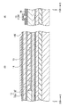
図1〜図12において、(A)はエアベアリング面に垂直な断面構造を示し、(B)は磁極部分のエアベアリング面に平行な断面構造を示している。図13〜図20は主要な製造工程に対する斜視構造、図21は薄膜コイル9、下部磁極13および上部磁極17の完成状態における平面構造、図22は完成状態における薄膜コイル9の構造を1本の線状に簡略化して表したものである。ここで、図13〜図20において、図13は図2,図14は図4,図15は図5,図16は図6,図17は図7,図18は図8,図19は図9,図20は図10に示した状態にそれぞれ対応している。上記した図2〜図10の(A)は、図13〜図20におけるA−A線に沿った矢視断面に相当する。
【0018】
以下の説明では、図1〜図22の各図中におけるX軸方向を「幅(または幅方向)」、Y軸方向を「長さ(または長さ方向)」、Z軸方向を「厚み(または厚み方向)」と表記すると共に、Y軸方向のうち、エアベアリング面20側(または後工程においてエアベアリング面20となる側)を「前側(または前方」、その反対側を「後側(または後方)」と表記するものとする。
【0019】
<薄膜磁気ヘッドの製造方法>
本実施の形態の薄膜磁気ヘッドの製造方法では、まず、図1に示したように、例えばアルティック(Al2 O3 ・TiC)からなる基板1上に、例えば酸化アルミニウム(Al2 O3 ;以下、単に「アルミナ」という。)よりなる絶縁層2を約3.0μm〜5.0μm程度の厚みで堆積する。次に、絶縁層2上に、例えば後述するフレームめっき法により、例えばニッケル鉄合金(NiFe:以下、単に「パーマロイ(商品名)という。」)よりなる下部シールド層3を約2.0μmの厚みで選択的に形成する。
【0020】
次に、図1に示したように、下部シールド層3上に、例えばスパッタリングにより、例えばアルミナよりなるシールドギャップ膜4を約0.01μm〜0.1μmの厚みで形成する。次に、シールドギャップ膜4上に、高精度のフォトリソグラフィ処理により、MR素子を構成するためのMR膜5を所望のパターン形状となるように形成する。次に、高精度のフォトリソグラフィ処理により、MR膜5と電気的に接続する引き出し電極層としてのリード層(図示せず)を選択的に形成する。次に、シールドギャップ膜4を形成した場合と同様の手法によりMR膜5を覆うようにシールドギャップ膜6を形成し、MR膜5等をシールドギャップ膜4,6内に埋設する。
【0021】
次に、シールドギャップ膜4,6上に、例えばフレームめっき法により、例えばパーマロイよりなる上部シールド層7を約1.0μm〜2.0μmの厚みで選択的に形成する。
【0022】
次に、図2および図13に示したように、上部シールド層7上に、例えばスパッタリングにより、例えばアルミナよりなる絶縁膜8を約0.1μm〜0.2μmの厚みで選択的に形成する。絶縁膜8を形成する際には、後工程において他の上部シールド層10(図3参照)が形成されることとなる領域(開口部7K)を覆わないようにする。
【0023】
次に、図2および図13に示したように、絶縁膜8上に、例えばフレームめっき法により、例えば銅(Cu)よりなる複数のコイルパーツ9A(例えば9A1,9A2,9A3)を約1.0μm〜1.5μmの厚みで選択的に形成する。このコイルパーツ9Aは、後述する薄膜コイル9(図10および図20参照)の一部を構成することとなるものであり、例えば、図13に示したように、矩形をなした帯状の平面形状を有するものである。コイルパーツ9Aを形成する際には、後工程において形成される一連のコイルパーツ(9B,9C,9D,9E)と接続され、最終的にこれらのコイルパーツの集合体として薄膜コイル9が形成されるように位置合わせをする。より具体的には、例えば、コイルパーツ9Aの長手方向が、幅方向(図中のX軸方向)に対して傾くように配置する。なお、コイルパーツ9Aの平面形状は、必ずしも矩形状に限らず、自由に変更可能である。また、コイルパーツ9Aの配設個数は、下部磁極13および後述する上部磁極17(図8参照)に対する後述する薄膜コイル9の巻回数(巻き数)に応じて自由に変更可能である。
【0024】
フレームめっき法によりコイルパーツ9Aを形成する際には、まず、絶縁膜8上に、例えばスパッタリングにより、電解めっき法におけるシード層となる電極膜を形成する。電極膜の形成材料としては、例えば、コイルパーツ9Aの形成材料と同様の材料(銅)などを用いるようにする。次に、上記の電極膜上にフォトレジストを塗布してフォトレジスト膜を形成したのち、このフォトレジスト膜上に露光用のフォトマスクを選択的に形成する。フォトマスクを形成する際には、コイルパーツ9Aの平面形状に対応する平面形状を有するようにすると共に、コイルパーツ9Aの形成位置に対応するように位置合わせをする。次に、フォトマスクを用いてフォトレジスト膜に対して露光処理を施したのち、このフォトレジスト膜を現像することにより、コイルパーツ9Aを形成するための枠組み(フレームパターン)を選択的に形成する。次に、フレームパターンをマスクとして用いると共に、先工程において形成した電極膜をシード層として用いて、電解めっき法により銅をめっき成長させることによりコイルパーツ9Aを選択的に形成する。最後に、コイルパーツ9Aを形成したのち、フレームパターンを除去する。
【0025】
次に、図3に示したように、開口部7Kに、例えばフレームめっき法により、例えばパーマロイよりなる上部シールド層10を約2.5μm〜3.0μmの厚みで選択的に形成する。次に、コイルパーツ9Aおよび上部シールド層10等により構成された凹凸領域を覆うように、例えばスパッタリングにより、例えばアルミナよりなる前駆絶縁膜11Pを約3.0μm〜4.0μmの厚みで形成する。この前駆絶縁膜11Pは、後工程において研磨処理を施されることにより絶縁膜11となる前準備層である。
【0026】
次に、例えばCMP(化学機械研磨)法により、全体を研磨して平坦化することにより、図4および図14に示したように、コイルパーツ9A等を埋設する絶縁膜11を形成する。絶縁膜11を形成する際には、少なくとも上部シールド層10が露出するまで研磨処理を行うようにする。
【0027】
次に、図14に示したように、例えばリアクティブイオンエッチング(Reactive Ion Etching;以下、単に「RIE」という。)により、絶縁膜11のうち、コイルパーツ9A(9A1,9A2,9A3)の両端部近傍に対応する部分を選択的にエッチングして掘り下げることにより、例えば円形の開口形状を有する複数の接続ホール11Hを形成する。接続ホール11Hを形成する際には、コイルパーツ9Aが露出するまでエッチング処理を行うようにする。この接続ホール11Hは、コイルパーツ9Aと後工程において形成されるコイルパーツ9B(図17および図21参照)とを接続させるためのものである。なお、接続ホール11Hの開口形状は必ずしも円形に限らず、自由に変更可能である。
【0028】
次に、図5および図15に示したように、全体に、例えばスパッタリングにより、例えばアルミナよりなる絶縁膜12を約0.1μm〜0.2μmの厚みで形成する。絶縁膜12を形成する際には、図15に示したように、先工程において形成した接続ホール11Hを覆わないようにする。
【0029】
次に、図5および図15に示したように、絶縁膜12のうち、接続ホール11H群により囲まれた領域上に、例えばフレームめっき法により、全てのコイルパーツ9Aを横断するように例えばパーマロイよりなる下部磁極13を約2.0μm〜3.0μmの厚みで選択的に形成する。下部磁極13を形成する際には、例えば、図15に示したように、後工程においてエアベアリング面20となる側(図中の左側)から順に先端部13Aおよび後端部13Bを含むようにする。具体的な下部磁極13の構造としては、例えば、先端部13Aが、記録トラック幅を規定する極微小な一定幅を有するようにすると共に、後端部13Bが、その後方部においてほぼ一定の幅を有し、前方部において先端部13Aに近づくにつれて幅が狭まるようにする。
【0030】
次に、図6および図16に示したように、全体に、例えばスパッタリングにより、例えばアルミナよりなる記録ギャップ層14を約0.1μm〜0.3μmの厚みで形成する。記録ギャップ層14を形成する際には、下部磁極13と後工程において形成される上部磁極17(図8参照)とを接続させるための開口部14Kを覆わないようにする。
【0031】
次に、記録ギャップ層14上に、高精度のフォトリソグラフィ処理により、加熱時に流動性を示す材料、例えばフォトレジストなどの有機絶縁材料を所定のパターンとなるように形成する。次に、このフォトレジスト膜に対して、約200℃〜250℃の範囲内における温度で加熱処理を施す。この加熱処理により、図6および図16に示したように絶縁膜15が選択的に形成される。この絶縁膜15は、主に、下部磁極13と後工程において形成されるコイルパーツ9Cとの間を電気的に絶縁するものである。加熱時にフォトレジストが流動することにより、絶縁膜15の端縁近傍は丸みを帯びた斜面をなす。絶縁膜15を形成する際には、例えば、後工程において形成されるコイルパーツ9C(図7および図17参照)の配設領域に対応するように位置合わせをすると共に、図16に示したように、先工程において形成した接続ホール11Hおよび開口部14Kを覆わないようにする。
【0032】
次に、図17に示したように、例えば電解めっき法により、接続ホール11H中に例えば銅よりなるめっき膜を成長させることにより、薄膜コイル9の一部を構成することとなる複数のコイルパーツ9Bを選択的に形成する。このコイルパーツ9Bは、図21に示したように、例えば、接続ホール11Hの内部構造に対応して円柱状の構造をなすように形成される。
【0033】
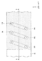
次に、図7および図17に示したように、例えばコイルパーツ9Aを形成した場合と同様のフレームめっき法により、例えば銅よりなる複数のコイルパーツ9C(例えば9C1,9C2,9C3,9C4,9C5,9C6,9C7)を約1.5μmの厚みで選択的に形成する。より具体的には、例えば、コイルパーツ9Cが矩形をなした帯状の平面形状を有するようにすると共に、コイルパーツ9Cの長手方向が長さ方向(図中のY軸方向)に対してほぼ直交するようにする。コイルパーツ9Cを形成する際には、コイルパーツ9C1の一端とコイルパーツ9A1の一端とがコイルパーツ9Bを介して接続されると共に、コイルパーツ9C2の他端とコイルパーツ9A1の他端とがコイルパーツ9Bを介して接続されるようにし、一連のコイルパーツ群(9C1,9B,9A1,9B,9C2)により構成される接続単位を形成する。そして、他のコイルパーツ群(9C3,9B,9A2,9B,9C4および9C5,9B,9A3,9B,9C6)についても同様に接続単位を形成する。各接続単位(コイルパーツ9A,9B,9C)は、図21に示したように、下部磁極13(後端部13B)の周囲を巻回することとなる。以下では、特に、コイルパーツ9A,9B,9Cにより構成される接続単位を「第1の巻回単位U1」と呼称するものとする(図22参照)。
【0034】
次に、図8および図18に示したように、コイルパーツ9Cおよびその周辺領域を覆うように、例えば絶縁膜15を形成した場合と同様の材料および形成方法を用いて、例えばフォトレジストよりなる絶縁膜16を形成する。コイルパーツ9Cは、絶縁膜16により埋設される。
【0035】
次に、図8および図18に示したように、後工程においてエアベアリング面20となる側から開口部14Kに至る領域上に、例えばフレームめっき法により、例えばパーマロイよりなる上部磁極17を約2.0μm〜3.0μmの厚みで選択的に形成する。上部磁極17を形成する際には、例えば、図18に示したように、下部磁極13(先端部13A,後端部13B)とほぼ同様の構造(先端部17A,後端部17B)を有し、厚み方向(図中のZ軸方向)において下部磁極13と対向するようにする。下部磁極13と上部磁極17とは開口部14Kにおいて磁気的に連結され、下部磁極13および上部磁極17により磁路が形成される。記録トラック幅を規定する極微小な一定幅を有する先端部13Aと先端部17Aとが記録ギャップ層14を介して対向することにより、磁極部分100が形成される(図8(B)参照)。
【0036】
次に、図9および図19に示したように、上部磁極17上に、例えば絶縁膜15を形成した場合と同様の材料および形成方法を用いて、例えばフォトレジストよりなる絶縁膜18を選択的に形成する。この絶縁膜18は、上部磁極17と後工程において形成されるコイルパーツ9Eとの間を電気的に絶縁するものである。絶縁膜18を形成する際には、後工程において形成されるコイルパーツ9E(図10,図20参照)の配設領域に対応するように位置合わせする。
【0037】
次に、図19に示したように、絶縁膜16,18および上部磁極17のうち、コイルパーツ9C1〜9C6におけるコイルパーツ9Bが配設されていない側の端部近傍に対応する部分およびコイルパーツ9C7の両端近傍に対応する部分を選択的にエッチングして掘り下げることにより、例えば円形の開口形状を有する複数の接続ホール18Hを形成する。接続ホール18Hを形成する際には、コイルパーツ9Cが露出するまでエッチング処理を行うようにする。この接続ホール18Hは、主に、コイルパーツ9Cと後工程において形成されるコイルパーツ9D(図20,図21参照)とを接続させるためのものである。
【0038】
次に、図20に示したように、例えば電解めっき法により、接続ホール18H中に例えば銅よりなるめっき膜を成長させることにより複数のコイルパーツ9Dを選択的に形成する。このコイルパーツ9Dは、例えば、図21に示したように、先工程において形成されたコイルパーツ9Bと同様に、接続ホール18Hの内部構造に対応して円柱状の構造をなすように形成される。
【0039】
次に、図10および図20に示したように、絶縁膜18上に、例えばフレームめっき法により、例えば銅よりなる複数のコイルパーツ9E(例えば9E1,9E2,9E3)を約1.5μmの厚みで選択的に形成する。コイルパーツ9Eを形成する際には、コイルパーツ9E1の一端とコイルパーツ9C2の一端とがコイルパーツ9Dを介して接続されると共に、コイルパーツ9E1の他端とコイルパーツ9C3の他端とがコイルパーツ9Dを介して接続されるようにし、一連のコイルパーツ群(9C2,9D,9E1,9D,9C3)により構成される接続単位を形成する。そして、他のコイルパーツ群(9C4,9D,9E2,9D,9C5および9C6,9D,9E3,9D,9C7)についても同様に接続単位を形成する。各接続単位(コイルパーツ9C,9D,9E)は、図21に示したように、上部磁極17(後端部17B)の周囲を巻回することとなる。以下では、特に、コイルパーツ9C,9D,9Eにより構成される接続単位を「第2の巻回単位U2」と呼称するものとする(図22参照)。なお、薄膜コイル9を形成する際には、例えば、下部磁極13および上部磁極17のそれぞれの周辺領域における磁束の発生量および後述する磁束の発生タイミングを均等化するために、第1の巻回単位U1の数と第2の巻回単位U2の数とを一致させるようにするのが好ましい(図22参照)。
【0040】
コイルパーツ9Eを形成することにより、一連のコイルパーツ(9A、9B,9C,9D,9E)の集合体として薄膜コイル9が形成される。コイルパーツ9Eを形成する際には、例えば、同時に、コイルパーツ9C1の他端部に形成されたコイルパーツ9DFと接続されるようにリード線9F1を形成すると共に、コイルパーツ9C7の一端部に形成されたコイルパーツ9DRと接続されるようにリード線9F2を形成する。リード線9F1,9F2の形成材料としては、例えば、薄膜コイル9と同様に銅などを用いるようにする。
【0041】
次に、図11に示したように、全体を覆うように、絶縁材料、例えばアルミナなどの無機絶縁材料よりなるオーバーコート層19を約20μm〜40μmの厚みで形成する。
【0042】
最後に、図12に示したように、機械加工や研磨工程により記録ヘッドおよび再生ヘッドのエアベアリング面20を形成して、薄膜磁気ヘッドが完成する。
【0043】
<薄膜磁気ヘッドの構造>
次に、図12、図21および図22を参照して、本実施の形態に係る薄膜磁気ヘッドの構造について説明する。
【0044】
図12に示したように、絶縁膜15の前端の位置は、記録ヘッドの性能を決定する因子の1つであるスロートハイト(TH)を決定する際の基準となる位置、すなわちスロートハイトゼロ位置(TH0位置)である。スロートハイト(TH)は、絶縁膜15の前端の位置(TH0位置)からエアベアリング面20までの長さとして規定される。
【0045】
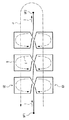
図21および図22に示したように、薄膜コイル9は、上記したように、積層形成された一連のコイルパーツ(9A,9B,9C,9D,9E)の集合体として構成されている。この薄膜コイル9は、エアベアリング面20から第1の巻回単位U1および第2の巻回単位U2を交互に連続して含み、下部磁極13(後端部13B)および上部磁極17(後端部17B)に交互に巻きつきながら延在する連続体をなしている。具体的には、例えば、第1の巻回単位U1では、薄膜コイル9が下部磁極13を中心として右回りに巻回し、第2の巻回単位2では、薄膜コイル9が上部磁極17を中心として左回りに巻回している。すなわち、エアベアリング面20側から見た薄膜コイル9の軌道は、「8」の字を描くようになっている(図22参照)。以下の説明では、主に、下部磁極13および上部磁極17の双方に均等に(バランスよく)コイルが巻きつく点に着目し、特に、薄膜コイル9の構造を「バランス巻き構造」と呼称することとする。薄膜コイル9の両端部に接続されたリード線9F1,9F2は、共に図示しない外部回路に接続されており、この外部回路により薄膜コイル9を導通させることができるようになっている。
【0046】
<薄膜磁気ヘッドの動作>
次に、図12、図21および図22を参照して、本実施の形態に係る薄膜磁気ヘッドの動作について説明する。
【0047】
この薄膜磁気ヘッドでは、情報の記録動作時において、図示しない外部回路を通じてリード線9F1から9F2に向かって薄膜コイル9に電流Iが流れると、これに応じて磁束Jが発生する。このとき、第1の巻回単位U1では、右回りに巻回するように電流Iが流れることにより、下部磁極13内を後方に向かって伝播する磁束Jの流れが生じ、一方、第2の巻回単位U2では、左回りに巻回するように電流Iが流れることにより、上部磁極17内を前方に向かって伝播する磁束Jの流れが生じる。これにより、薄膜コイル9により発生した磁束は、磁路内を下部磁極13から上部磁極17(先端部17A)に向かって伝播し、最終的に先端部17Aのエアベアリング面20側の先端部分に到達する。先端部17Aの先端部分に到達した磁束により、記録ギャップ層14近傍の外部に記録用の信号磁界が発生する。なお、リード線9F2から9F1に向かって逆方向に電流Iを流すことにより、磁路内を上部磁極17から下部磁極13に向かって磁束が伝播し、上記の場合と逆向きの信号磁界が発生する。これらの信号磁界により、磁気記録媒体を部分的に磁化して、情報を記録することができる。
【0048】
一方、情報の再生動作時においては、MR膜5にセンス電流を流す。MR膜5の抵抗値は、磁気記録媒体からの再生信号磁界に応じて変化するので、その抵抗変化をセンス電流の変化によって検出することにより、磁気記録媒体に記録されている情報を読み出すことができる。
【0049】
<本実施の形態の作用および効果>
次に、図12および図23を参照して、本実施の形態の作用および効果について説明する。図23は、本実施の形態の薄膜磁気ヘッドに対する比較例としての薄膜磁気ヘッドの断面構成を表すものであり、図12に対応するものである。図23では、例えば、薄膜コイル99が、上部磁極17(ヨーク部17B)の周囲を巻回するヘリカル構造を有する場合を示している。本実施の形態では、図12に示したように、薄膜コイル9が、第1の巻回単位U1および第2の巻回単位U2を交互に連続して含みながら下部磁極13および上部磁極17の延在方向に沿って延在するバランス巻き構造を有するようにしたので、以下のような理由により、薄膜磁気ヘッドの製造に要する時間を短縮すると共に製造歩留りを向上させることができる。
【0050】
すなわち、薄膜磁気ヘッドの小型化を実現するためには、コイルの巻線間を緊密にして薄膜コイルを小型化する必要がある。しかしながら、ヘリカル構造を有する薄膜コイル99を搭載した比較例としての薄膜磁気ヘッド(図23参照)を製造する場合には、コイルの占める領域(占有領域)がスパイラル構造を有する場合よりも小さいという点において利点が得られる一方、コイル巻線間を緊密にすると各巻線間距離D1が小さくなるため、薄膜コイル99の形成に際して高い形成精度が要求される。このような場合には、薄膜コイル99の形成精度が十分でなかったり、または薄膜コイル99の形成時において形成精度に微妙なずれが生じると、コイル巻線間の接触に起因して短絡等が生じ、薄膜磁気ヘッドの製造歩留りが低下する可能性がある。
【0051】
ここで、薄膜コイル99を高精度に形成する手法としては、例えば、薄膜コイル99の形成領域における下地の表面を研磨処理を用いて平坦化する方法がある。これは、例えばフレームめっき法を用いて薄膜コイルを形成する際に、下地の表面が凹凸をなしていると、フレームパターンを形成するための露光工程において下地の表面から斜め方向や横方向に反射する反射光に起因してフレームパターンの形成精度が低下するため、下地の表面を研磨して平坦化することにより反射光による悪影響を抑制するものである。ところが、研磨処理を行うと製造工程数が増加するため、薄膜磁気ヘッドの製造に要する時間が長くなってしまう。すなわち、比較例の場合には、薄膜コイル99の小型化と製造歩留り等の向上とを両立させることは困難であった。
【0052】
これに対して、本実施の形態では、図12に示したように、コイルの小型化に応じてコイルパーツ9C間の距離D2(ほぼD2=D1)は狭まるが、コイルパーツ9A間の距離D3およびコイルパーツ9E間の距離D4(ほぼD3=D4)は十分な距離が確保される。このような場合には、コイルパーツ9Cの形成に関しては高い形成精度が要求されるが、コイルパーツ9A,9Eの形成に関してはコイルパーツ9Cの形成に要するほどの形成精度を必要としない。したがって、本実施の形態では、上記した比較例の場合(薄膜コイル99を形成する場合)よりも、薄膜コイル9のうち、高い形成精度が要求される部分の割合が減少するため、短絡等の不具合が生じる可能性が低下し、薄膜コイルの製造歩留りが向上する。しかも、バランス巻き構造を有する薄膜コイル9の占める領域(占有領域)は、ヘリカル構造を有する薄膜コイル(例えば薄膜コイル99)の占有領域よりは若干大きくなるが、スパイラル構造を有する薄膜コイルに比べるとその占有領域は大幅に小さくなるため、薄膜コイル9の小型化も実現することができる。
【0053】
さらに、本実施の形態では、コイルパーツ9A,9Eの形成に高い形成精度を要しないことに基づき、これらの部位の形成工程において研磨処理を行う必要がないため、薄膜コイル9の形成を容易化することにより製造工程数を削減し、薄膜磁気ヘッドの製造に要する時間を短縮することができる。すなわち、本実施の形態薄膜磁気ヘッドでは、従来の技術の項において例示した薄膜磁気ヘッド(特開平5−242429,実用新案第3033043号,特開平5−101337)とは異なり、コイルの小型化と製造歩留り等の向上とを適正に両立させることができる。
【0054】
また、本実施の形態では、磁束の発生タイミングに起因するノイズ成分の発生の抑制に係る観点においても利点を有する。図24は本実施の形態の薄膜磁気ヘッドの構造、図25は本実施の形態の薄膜磁気ヘッドに対する他の比較例としての薄膜磁気ヘッドの構造をそれぞれ模式的に示したものである。図25に示した薄膜コイル109(例えば巻き数6回)は、ヘリカル構造を有するものであり、下部磁極13の周囲をその延在方向に沿って巻回する巻回単位U3A,U3B,U3Cと、上部磁極17の周囲をその延在方向に沿って巻回する巻回単位U4A,U4B,U4Cとが連結された連続体をなしている。この薄膜コイル109では、電流を流した際の磁束の発生状態が不均等になる。すなわち、薄膜コイル109に電流を流すと、磁束の発生領域は巻回単位U3A,U3B,U3C,U4C,U4B,U4Aの順に移行し、下部磁極13の領域(U3A,U3B,U3C)において磁束が発生したのち、上部磁極17の領域(U4A,U4B,U4C)において磁束が発生することとなる。このような場合には、下部磁極13と上部磁極17とで磁束の発生タイミングが大きく異なってしまうため、不均一な磁壁の移動が生じ、ポップコーンノイズなどのライトアフターノイズが発生してしまう。
【0055】
これに対して、本実施の形態(図24参照)では、薄膜コイル109と同一の巻き数(6回)を有するとすると、磁束の発生領域は、U1A,U2A,U1B,U2B,U1C,U2Cの順に移行し、下部磁極13と上部磁極17とを含めた磁極全体として磁束の発生タイミングが均等化される。これにより、上記した比較例の場合とは異なり、ポップコーンなどのライトアフターノイズの発生を抑制することができる。
【0056】
また、本実施の形態では、薄膜コイル9がバランス巻き構造を有することにより、上記したノイズ成分の発生の抑制の他、記録特性の安定化という利点も有することとなる。図26は、本実施の形態の薄膜磁気ヘッドに対するさらに他の比較例としての薄膜磁気ヘッドの構造を模式的に示したものであり、薄膜コイル209が例えばスパイラル構造を有している。スパイラル構造を有する薄膜コイル209では、磁路構成部品(下部磁極13,上部磁極17)への磁束Jの収容効率、すなわち、薄膜コイル209により発生した磁束量J1に対する磁路構成部品に収容される磁束量J2の割合(J2/J1)が十分ではない。なぜなら、薄膜コイル209により発生した磁束Jのうち、下部磁極13および上部磁極17よりも後方に発生した磁束Jが磁路構成部品に収容されにくいからである。
【0057】
これに対して、本実施の形態(図24参照)では、薄膜コイル9の全ての部分が下部磁極13および上部磁極17に近接して周囲を巻回しているため、薄膜コイル9により発生した磁束Jが磁路構成部品に十分に収容され、磁路構成部品への磁束Jの収容効率が向上する。これにより、上部磁極17の先端部17Aにおける磁束密度が増大し、安定した記録特性を確保することができる。
【0058】
また、本実施の形態では、薄膜磁気ヘッドの高周波応答特性の観点においても利点を有する。すなわち、一般に、薄膜磁気ヘッドの高周波応答特性は、薄膜コイルのコイルインダクタンスが小さくなるほど向上する。薄膜コイルのコイルインダクタンスは、例えば、薄膜コイルのうちのリング状をなす部分の半径(コイル半径)が小さくなるにつれて減少することが知られている。スパイラル構造を有する薄膜コイル209(図26参照)では、コイルの巻き数の増加に応じてコイル半径が増大するため、コイルインダクタンスが大きくなり、高周波応答特性が劣化してしまう。これに対して、本実施の形態の薄膜コイル9(図24参照)では、薄膜コイル209の場合よりもコイル半径が小さくなり、コイルの巻き数を増加させた場合においてもコイル半径が維持されるため、コイルインダクタンスを小さくし、高周波応答特性を向上させることができる。
【0059】
このことは、図27に示した薄膜磁気ヘッドの励磁磁界特性に関する実験結果から明らかである。図27は、励磁磁界Lの立ち上がり特性に関する実験結果である。図中の「横軸」は時間T,「縦軸」は励磁磁界の強さLをそれぞれ表し、「A」はバランス巻き構造を有する薄膜コイル9を搭載した本実施の形態の薄膜磁気ヘッド(図24参照),「B」はスパイラル構造を有する薄膜コイルを搭載した比較例としての薄膜磁気ヘッド(図26参照)の特性をそれぞれ表している。なお、「A」および「B」の薄膜磁気ヘッドにおける磁束の発生量は同一である。図27に示したように、本実施の形態の薄膜磁気ヘッド(A)における励磁磁界Lの立ち上がり勾配の方が、比較例としての薄膜磁気ヘッド(B)における励磁磁界Lの立ち上がり勾配よりも急峻であり、より短時間で安定する。
【0060】
なお、本実施の形態では、5種類のコイルパーツ(9A〜9E)の集合体として薄膜コイル9を構成するようにしたが、必ずしもこれに限られるものではなく、薄膜コイル9を構成するコイルパーツの種類の数は自由に変更可能である。具体的には、例えば、図28に示したように、コイルパーツ9Bおよび9Cを「9Gと」して一体形成すると共に、コイルパーツ9Dおよび9Eを「9H」として一体形成し、3種類のコールパーツ(9A,9G,9H)により薄膜コイル9が構成されるようにしてもよい。コイルパーツ数を少なくすることにより、薄膜コイル9の形成に要する製造工程数が削減されるため、薄膜磁気ヘッドの製造に要する時間を短縮することができる。なお、図28に示した薄膜磁気ヘッドにおける上記以外の構造は、図21の場合と同様である。
【0061】
また、本実施の形態では、図21および図22に示したように、第1の巻回単位U1において薄膜コイル9が下部磁極13を中心として右回りに巻回し、第2の巻回単位U2において薄膜コイル9が上部磁極17を中心として左回りに巻回するようにしたが、必ずしもこれに限られるものではなく、第1の巻回単位U1および第2の巻回単位U2における薄膜コイル9の巻回方向を逆にするようにしてもよい。このような場合においても、上記実施の形態の場合と同様の効果を得ることができる。
【0062】
また、本実施の形態では、薄膜コイル9が第1の巻回単位U1において下部磁極13の周囲を巻回し、第2の巻回単位U2において上部磁極17の周囲を巻回するようにしたが、必ずしもこれに限られるものではなく、第1の巻回単位U1において上部磁極17の周囲を巻回し、第2の巻回単位U2において下部磁極13の周囲を巻回するようにしてもよい。
【0063】
また、本実施の形態では、第1の巻回単位U1において薄膜コイル9が下部磁極13の周囲を1回巻回し、第2の巻回単位U2において薄膜コイル9が上部磁極17の周囲を1回巻回するようにしたが、各巻回単位(U1,U2)における薄膜コイル9の巻回数は自由に変更可能である。具体的には、例えば、第1の巻回単位U1および第2の巻回単位U2における巻回数を複数回としてもよいし、第1の巻回単位U1と第2の巻回単位U2とで巻回数が異なるようにしてもよい。ただし、薄膜コイル9の巻回数を変更する場合には、上記したように、下部磁極13周辺における磁束の発生量と上部磁極17周辺における磁束の発生量とを均等にすべく、第1の巻回単位U1における総巻回数と第2の巻回単位U2における総巻回数とを同一にするのが好ましい。
【0064】
以上、実施の形態を挙げて本発明を説明したが、本発明は上記実施の形態に限定されるものではなく、種々変形することができる。例えば、上記実施の形態では、本発明のコイル構造(バランス巻き構造)を薄膜磁気ヘッドに搭載される薄膜コイルに適用した場合について説明したが、必ずしもこれに限られるものではなく、薄膜磁気ヘッドの他、これと同様の構造(対向する2つの磁性体と磁束発生用のコイル)および動作機構(記録,再生)を有する他の磁気ヘッド(例えばビデオヘッド等)にも適用可能である。このような場合においても、上記実施の形態の場合と同様の効果を得ることができる。
【0065】
また、上記実施の形態では、薄膜コイル9がバランス巻き構造のみを有する場合について説明したが、必ずしもこれに限られるものではなく、例えば、薄膜コイル9が、バランス巻き構造の他、スパイラル構造またはヘリカル構造を含むようにしてもよい。もちろん、薄膜コイル9がバランス巻き構造,スパイラル構造,ヘリカル構造の全てを含むようにしてもよい。
【0066】
また、上記実施の形態における下部磁極13および上部磁極17を含む一連の構成要素の平面形状は必ずしも図15や図18に示したものに限られるものではなく、各構成要素の機能を確保することが可能な限りにおいて、一連の構成要素の平面形状は自由に変更可能である。
【0067】
また、薄膜磁気ヘッドを構成する一連の構成要素の形成に係る形成方法および形成材料等は、必ずしも上記実施の形態において説明したものに限らず、各構成要素の構造的特徴および材質的特徴等を再現することが可能な限り、一連の構成要素の形成方法や形成材料等は自由に変形可能である。
【0068】
また、例えば、上記実施の形態では、複合型薄膜磁気ヘッドについて説明したが、本発明は、書き込み用の誘導型磁気変換素子を有する記録専用の薄膜磁気ヘッドや記録・再生兼用の誘導型磁気変換素子を有する薄膜磁気ヘッドにも適用することができる。また、本発明は、書き込み用の素子と読み出し用の素子の積層順序を逆転させた構造の薄膜磁気ヘッドにも適用することができる。
【0069】
【発明の効果】
以上説明したように、請求項1ないし請求項7のいずれか1項に記載の薄膜磁気ヘッドまたは請求項8に記載の薄膜磁気ヘッドの製造方法によれば、下部磁極および上部磁極が、ギャップ層を介して互いに対向する部分と互いに磁気的に連結される部分とを結ぶ直線上に沿って延在し、薄膜コイルが、記録媒体対向面から見て8の字を描くと共に各第1の巻回単位同士および各第2の巻回単位同士が互いに重ならないように第1の巻回単位と第2の巻回単位とを交互に連結してなる連続体をなし、第1の巻回単位の数と第2の巻回単位の数とが互いに一致するようにしたので、薄膜コイルのうち、高い形成精度を要する部分の割合が減少する。また、下部磁極および上部磁極のそれぞれの周辺領域における磁束の発生量および発生タイミングが均等化する。したがって、薄膜コイルを小型化しつつ、薄膜磁気ヘッドの製造に要する時間を短縮することができると共に製造歩留りを向上させることができる。
【図面の簡単な説明】
【図1】本発明の一実施の形態に係る薄膜磁気ヘッドの製造方法における一工程を説明するための断面図である。
【図2】図1に続く工程を説明するための断面図である。
【図3】図2に続く工程を説明するための断面図である。
【図4】図3に続く工程を説明するための断面図である。
【図5】図4に続く工程を説明するための断面図である。
【図6】図5に続く工程を説明するための断面図である。
【図7】図6に続く工程を説明するための断面図である。
【図8】図7に続く工程を説明するための断面図である。
【図9】図8に続く工程を説明するための断面図である。
【図10】図9に続く工程を説明するための断面図である。
【図11】図10に続く工程を説明するための断面図である。
【図12】図11に続く工程を説明するための断面図である。
【図13】図2に示した状態に対応する平面図である。
【図14】図4に示した状態に対応する平面図である。
【図15】図5に示した状態に対応する平面図である。
【図16】図6に示した状態に対応する平面図である。
【図17】図7に示した状態に対応する平面図である。
【図18】図8に示した状態に対応する平面図である。
【図19】図9に示した状態に対応する平面図である。
【図20】図10に示した状態に対応する平面図である。
【図21】薄膜コイル、下部磁極および上部磁極の完成状態を表す斜視図である。
【図22】薄膜コイルの構造を簡略化して表す図である。
【図23】本実施の形態の薄膜磁気ヘッドに対する比較例としての薄膜磁気ヘッドの構造を表す断面図である。
【図24】本実施の形態の薄膜磁気ヘッドの構造を模式的に表す図である。
【図25】本実施の形態の薄膜磁気ヘッドに対する他の比較例としての薄膜磁気ヘッドの構造を模式的に表す図である。
【図26】本実施の形態の薄膜磁気ヘッドに対するさらに他の比較例としての薄膜磁気ヘッドの構造を模式的に表す図である。
【図27】励磁磁界特性に関する実験結果を表す図である。
【図28】本実施の形態の薄膜磁気ヘッドの構造に係る変形例を表す斜視図である。
【符号の説明】
1…基板、2,11…絶縁層、3…下部シールド層、4,6…シールドギャップ膜、5…MR膜、7,10…上部シールド層、8,12,15,16,18…絶縁膜、9,99,109,209…薄膜コイル、9A(9A1,9A2,9A3),9B,9C(9C1,9C2,9C3,9C4,9C5,9C6,9C7),9D,9E(9E1,9E2,9E3),9G,9H…コイルパーツ、9F1,9F2…リード線、11H,18H…接続ホール、11P…前駆絶縁層、13…下部磁極、13A,17A…先端部、13B,17B…後端部、14…記録ギャップ層、19…オーバーコート層、20…エアベアリング面、100…磁極部分、I…電流、J…磁束、TH…スロートハイト、U1(U1A,U1B,U1C)…第1の巻回単位、U2(U2A,U2B,U2C)…第2の巻回単位。[0001]
BACKGROUND OF THE INVENTION
The present invention has at least an inductive magnetic transducer for writing.Thin filmThe present invention relates to a magnetic head and a manufacturing method thereof.
[0002]
[Prior art]
In recent years, with the improvement in the surface recording density of hard disk devices, there has been a demand for improved performance of thin film magnetic heads. As the thin film magnetic head, for example, a structure in which a recording head having an inductive magnetic conversion element for writing and a reproducing head having a magnetoresistive (hereinafter referred to as MR (Magneto Resistive)) element is stacked. The composite type thin film magnetic head is widely used.
[0003]
The recording head, for example, is arranged above and below a write gap, and is magnetically coupled at one end to an upper magnetic pole (top pole) and a lower magnetic pole (bottom pole), for generating magnetic flux. And a coil. The upper magnetic pole and the lower magnetic pole have the same constant width (constant) in the vicinity of the recording gap in the region near the recording medium facing surface (air bearing surface) facing the magnetic recording medium (hereinafter simply referred to as “recording medium”). These portions constitute a “magnetic pole portion” that defines the recording track width.
[0004]
The coil structure may be, for example, a “spiral structure” wound two-dimensionally (in a single plane) around the upper magnetic pole, the lower magnetic pole, or the connection between the upper magnetic pole and the lower magnetic pole, or the upper magnetic pole or the lower magnetic pole. There are known "helical structures" that wrap around the door. As an example to which these coil structures are applied, for example, in Japanese Patent Laid-Open No. 5-242429, in a thin film magnetic head having an upper magnetic core and a lower magnetic core arranged opposite to each other, a lower striped conductive film, an upper striped conductive film, etc. There is disclosed a structure in which a helical conductor coil configured is wound around the upper magnetic core. In addition, in Utility Model No. 3030343, in a thin film magnetic head including a first core and a second core arranged to face each other, the periphery of the first core is wound clockwise (or counterclockwise) and the periphery of the second core. Turn counterclockwise(Or rightA structure is disclosed in which a plurality of spiral thin film coil layers that are wound around are arranged hierarchically and these thin film coil layers are connected to each other. In JP-A-5-101337, in a thin film magnetic head having a lower layer thin film magnetic core and an upper layer thin film magnetic core arranged opposite to each other, a helical coil wound around the lower layer thin film magnetic core and the periphery of the upper layer thin film magnetic core are arranged. A structure in which a helical coil to be wound is connected via a spiral coil is disclosed.
[0005]
In a thin film magnetic head, for example, when a current flows through a coil during an information recording operation, a magnetic flux is generated accordingly. The magnetic flux generated at this time propagates to a constant width portion of the upper magnetic pole constituting a part of the magnetic pole portion via a magnetic flux propagation path (hereinafter referred to as “magnetic path”) constituted by the upper magnetic pole and the lower magnetic pole. To do. The magnetic flux propagated to the constant width portion further reaches the tip of the air bearing surface side. When the magnetic flux reaching the tip of the constant width portion leaks to the outside in the vicinity of the recording gap, a recording signal magnetic field is generated. The recording medium is partially magnetized by this signal magnetic field, and information is recorded.
[0006]
[Problems to be solved by the invention]
By the way, in recent years, for the purpose of downsizing a thin film magnetic head, for example, downsizing of a coil is required. When considering miniaturization of the coil, a helical structure in which the coil occupies a smaller area is more suitable as a coil structure than a spiral structure having a two-dimensional extension. It is considered possible to further reduce the size.
[0007]
Conventionally, however, there have been problems that it takes a long time to manufacture a thin film magnetic head and the manufacturing yield is lowered for the following reasons. That is, for example, in order to close the coil windings in order to reduce the size of the coil, high formation accuracy is required. In such a case, the manufacturing process of the coil becomes complicated in order to ensure high formation accuracy, so that the time required for manufacturing the thin film magnetic head becomes long. In addition, if the coil formation accuracy is not sufficient, or if there is a slight shift in the formation accuracy during coil formation, a short circuit or the like occurs due to contact between the coil windings, and the manufacturing yield of the thin film magnetic head decreases. there is a possibility. That is, conventionally, it has been difficult to properly achieve both a reduction in the size of the coil and an improvement in manufacturing yield.
[0008]
In addition to the thin-film magnetic head, the above problem also occurs in other magnetic heads having the same structure (two opposing magnetic bodies and a coil for generating magnetic flux) (for example, a head for recording and reproducing video tape). It happens in the same way.
[0009]
The present invention has been made in view of such problems, and its object is to reduce the manufacturing time and improve the manufacturing yield while reducing the size of the coil.Thin filmAn object of the present invention is to provide a magnetic head and a manufacturing method thereof.
[0010]
[Means for Solving the Problems]
The thin film magnetic head of the present invention extends from the recording medium facing surface facing the recording medium in a direction away from this surface so as to face each other in the film thickness direction, and a gap is formed at the end near the recording medium facing surface. A lower magnetic pole and an upper magnetic pole, which are opposed to each other through the layer and are magnetically coupled to each other at an end far from the recording medium facing surface, and a plurality of first windings wound around the lower magnetic pole in a predetermined direction A thin film coil including a winding unit and a plurality of second winding units wound in a direction opposite to a predetermined direction around the upper magnetic pole, and extending along the extending direction of the lower magnetic pole and the upper magnetic pole; A thin film magnetic head having an insulating layer for insulating a thin film coil from a lower magnetic pole and an upper magnetic pole;The lower magnetic pole and the upper magnetic pole extend along a straight line connecting a portion facing each other through a gap layer and a portion magnetically coupled to each other;The first winding unit and the second winding are formed so that the thin-film coil draws a figure 8 when viewed from the recording medium facing surface, and the first winding units and the second winding units do not overlap each other. A continuous body is formed by alternately connecting units, and the number of first winding units and the number of second winding units are made to coincide with each other.
[0011]
In the thin film magnetic head of the present invention,When the lower magnetic pole and the upper magnetic pole extend along a straight line connecting a portion facing each other through a gap layer and a portion magnetically coupled to each other,The thin film coil draws a figure 8 when viewed from the recording medium facing surface, and the first winding unit and the second winding unit so that the first winding units and the second winding units do not overlap each other. A continuous body is formed by alternately connecting the winding units, and the number of first winding units and the number of second winding units coincide with each other. Thereby, the ratio of the part which requires high formation accuracy among thin film coils decreases. Further, the generation amount and generation timing of the magnetic flux in the peripheral regions of the lower magnetic pole and the upper magnetic pole are equalized.
[0012]
In the thin-film magnetic head of the present invention, the thin-film coils have a plurality of strip-shaped first coil parts arranged at a level below the lower magnetic pole, and a plurality of belt-like shapes arranged at a level between the lower magnetic pole and the upper magnetic pole. Second coil parts, a plurality of strip-shaped third coil parts arranged in a layer above the upper magnetic pole, and a plurality of columnar fourths for connecting the ends of the first and second coil parts to each other. And a plurality of columnar fifth coil parts for connecting the ends of the second and third coil parts to each other. In this case, the first to fifth coil parts are formed separately, the second coil part extends along the recording track width direction, and the first and third coil parts have the recording track width. The first coil part may be formed separately from the second to fifth coil parts, and the second and fourth coil parts may be integrated with each other. The third and fifth coil parts are integrally formed, and the integrally formed second and fourth coil parts extend in the recording track width direction, and the first coil part and the first coil part are integrally formed. The third and fifth coil parts may be inclined and extend with respect to the recording track width direction. Also, the bottom pole and top pole,RecordIn order from the side closer to the recording medium facing surface, a portion having a constant width that defines the recording track width and a portion having a larger width may be included.
[0013]
The method for manufacturing a thin film magnetic head of the present invention extends from a recording medium facing surface facing a recording medium in a direction away from this surface so as to face each other in the film thickness direction, and is on an end near the recording medium facing surface. A lower magnetic pole and an upper magnetic pole that are opposed to each other through a gap layer and are magnetically coupled to each other at an end remote from the recording medium facing surface, and a plurality of windings wound in a predetermined direction with the lower magnetic pole as a center. A thin film including a first winding unit and a plurality of second winding units wound in a direction opposite to a predetermined direction around the upper magnetic pole and extending along the extending direction of the lower magnetic pole and the upper magnetic pole A method of manufacturing a thin film magnetic head having a coil and an insulating layer that insulates the thin film coil from a lower magnetic pole and an upper magnetic pole;Forming a lower magnetic pole and an upper magnetic pole so as to extend along a straight line connecting a portion facing each other through a gap layer and a portion magnetically coupled to each other;By forming a plurality of constituent elements constituting the thin film coil in order, a figure 8 is drawn when viewed from the recording medium facing surface, and each of the first winding units and each of the second winding units are formed. A thin film coil is formed so as to form a continuous body in which the first winding unit and the second winding unit are alternately connected so as not to overlap each other, and the number of the first winding unit and the second winding unit are formed. The number of times is made to match each other.
[0014]
In the method of manufacturing the thin film magnetic head of the present invention,When the lower magnetic pole and the upper magnetic pole are formed so as to extend along a straight line connecting a portion facing each other and a portion magnetically coupled to each other through the gap layer,By forming a plurality of constituent elements constituting the thin film coil in order, a figure 8 is drawn when viewed from the recording medium facing surface, and the first winding units and the second winding units are drawn. The first winding unit and the second winding unit are alternately connected so that they do not overlap each other, and the number of the first winding unit and the number of the second winding unit are Thin film coils are formed so as to coincide with each other.
[0015]
DETAILED DESCRIPTION OF THE INVENTION
Hereinafter, embodiments of the present invention will be described in detail with reference to the drawings.
[0016]
First, a method for manufacturing a composite thin film magnetic head as a method for manufacturing a thin film magnetic head according to an embodiment of the present invention will be described with reference to FIGS. The thin film magnetic head according to the present embodiment is embodied by the method of manufacturing a thin film magnetic head according to the present embodiment, and will be described below.
[0017]
1 to 12, (A) shows a cross-sectional structure perpendicular to the air bearing surface, and (B) shows a cross-sectional structure parallel to the air bearing surface of the magnetic pole portion. 13 to 20 are perspective views of main manufacturing processes, and FIG. 21 is a completed state of the
[0018]
In the following description, the X-axis direction in each of FIGS. 1 to 22 is “width (or width direction)”, the Y-axis direction is “length (or length direction)”, and the Z-axis direction is “thickness (or length)”. Or in the Y-axis direction, the
[0019]
<Method for Manufacturing Thin Film Magnetic Head>
In the method of manufacturing a thin film magnetic head according to the present embodiment, first, as shown in FIG.2OThreeOn the
[0020]
Next, as shown in FIG. 1, a shield gap film 4 made of alumina, for example, is formed on the
[0021]
Next, the
[0022]
Next, as shown in FIGS. 2 and 13, an insulating
[0023]
Next, as shown in FIGS. 2 and 13, a plurality of
[0024]
When forming the
[0025]
Next, as shown in FIG. 3, the
[0026]
Next, the whole is polished and flattened by, for example, a CMP (Chemical Mechanical Polishing) method, thereby forming the insulating
[0027]
Next, as shown in FIG. 14, both ends of the
[0028]
Next, as shown in FIGS. 5 and 15, an insulating
[0029]
Next, as shown in FIGS. 5 and 15, over the region surrounded by the
[0030]
Next, as shown in FIGS. 6 and 16, a
[0031]
Next, a material that exhibits fluidity when heated, for example, an organic insulating material such as a photoresist, is formed on the
[0032]
Next, as shown in FIG. 17, a plurality of coil parts that constitute a part of the
[0033]
Next, as shown in FIGS. 7 and 17, for example, a plurality of
[0034]
Next, as shown in FIGS. 8 and 18, for example, a photoresist is used by using the same material and the same forming method as that for forming the insulating
[0035]
Next, as shown in FIGS. 8 and 18, the upper
[0036]
Next, as shown in FIGS. 9 and 19, the insulating
[0037]
Next, as shown in FIG. 19, portions of the insulating
[0038]
Next, as shown in FIG. 20, a plurality of
[0039]
Next, as shown in FIGS. 10 and 20, a plurality of
[0040]
By forming the
[0041]
Next, as shown in FIG. 11, an
[0042]
Finally, as shown in FIG. 12, the
[0043]
<Structure of thin film magnetic head>
Next, the structure of the thin film magnetic head according to the present embodiment will be described with reference to FIG. 12, FIG. 21, and FIG.
[0044]
As shown in FIG. 12, the position of the front end of the insulating
[0045]
As shown in FIGS. 21 and 22, the
[0046]
<Operation of thin-film magnetic head>
Next, the operation of the thin film magnetic head according to the present embodiment will be described with reference to FIG. 12, FIG. 21, and FIG.
[0047]
In this thin film magnetic head, when a current I flows through the
[0048]
On the other hand, a sense current is passed through the
[0049]
<Operation and effect of the present embodiment>
Next, with reference to FIG. 12 and FIG. 23, the effect | action and effect of this Embodiment are demonstrated. FIG. 23 shows a cross-sectional configuration of a thin film magnetic head as a comparative example with respect to the thin film magnetic head of the present embodiment, and corresponds to FIG. FIG. 23 shows a case where the
[0050]
That is, in order to realize the miniaturization of the thin film magnetic head, it is necessary to reduce the size of the thin film coil by tightly connecting the coil windings. However, when manufacturing a thin film magnetic head (see FIG. 23) as a comparative example equipped with a
[0051]
Here, as a method of forming the
[0052]
On the other hand, in the present embodiment, as shown in FIG. 12, the distance D2 (approximately D2 = D1) between the
[0053]
Furthermore, in the present embodiment, since it is not necessary to form the
[0054]
In addition, the present embodiment has an advantage from the viewpoint of suppressing the generation of noise components due to the generation timing of magnetic flux. FIG. 24 schematically shows the structure of the thin film magnetic head of this embodiment, and FIG. 25 schematically shows the structure of a thin film magnetic head as another comparative example with respect to the thin film magnetic head of this embodiment. The thin film coil 109 (for example, 6 turns) shown in FIG. 25 has a helical structure, and winding units U3A, U3B, U3C for winding around the lower
[0055]
On the other hand, in this embodiment (see FIG. 24), assuming that the
[0056]
In the present embodiment, since the thin-
[0057]
On the other hand, in the present embodiment (see FIG. 24), all portions of the
[0058]
The present embodiment also has an advantage in terms of the high frequency response characteristics of the thin film magnetic head. That is, generally, the high-frequency response characteristics of a thin film magnetic head improve as the coil inductance of the thin film coil decreases. For example, it is known that the coil inductance of a thin film coil decreases as the radius (coil radius) of a ring-shaped portion of the thin film coil decreases. In the
[0059]
This is clear from the experimental results regarding the exciting magnetic field characteristics of the thin film magnetic head shown in FIG. FIG. 27 shows the experimental results regarding the rising characteristics of the excitation magnetic field L. FIG. In the figure, the “horizontal axis” represents time T, the “vertical axis” represents the intensity L of the excitation magnetic field, and “A” represents the thin film magnetic head of the present embodiment on which the
[0060]
In the present embodiment, the
[0061]
In the present embodiment, as shown in FIGS. 21 and 22, the
[0062]
In the present embodiment, the thin-
[0063]
Further, in the present embodiment, the
[0064]
While the present invention has been described with reference to the embodiment, the present invention is not limited to the above embodiment, and various modifications can be made. For example, in the above-described embodiment, the case where the coil structure (balance winding structure) of the present invention is applied to a thin film coil mounted on a thin film magnetic head has been described. In addition, the present invention can also be applied to other magnetic heads (for example, a video head) having the same structure (two opposing magnetic bodies and coils for generating magnetic flux) and an operation mechanism (recording and reproducing). Even in such a case, the same effect as in the case of the above-described embodiment can be obtained.
[0065]
In the above embodiment, the case where the
[0066]
Further, the planar shape of a series of components including the lower
[0067]
In addition, the forming method and the forming material relating to the formation of a series of constituent elements constituting the thin film magnetic head are not necessarily limited to those described in the above embodiment, but the structural characteristics and material characteristics of each constituent element are described. As long as it can be reproduced, a method of forming a series of constituent elements, a forming material, and the like can be freely modified.
[0068]
Further, for example, in the above-described embodiment, the composite type thin film magnetic head has been described. However, the present invention can be applied to a recording-only thin film magnetic head having an inductive magnetic conversion element for writing or an inductive magnetic conversion for both recording and reproduction. The present invention can also be applied to a thin film magnetic head having an element. The present invention can also be applied to a thin film magnetic head having a structure in which the stacking order of a writing element and a reading element is reversed.
[0069]
【The invention's effect】
As described above,
[Brief description of the drawings]
FIG. 1 is a cross-sectional view for explaining one step in a method of manufacturing a thin film magnetic head according to an embodiment of the invention.
FIG. 2 is a cross-sectional view for explaining a step following the step in FIG. 1;
FIG. 3 is a cross-sectional view for explaining a step following the step of FIG. 2;
4 is a cross-sectional view for explaining a process following the process in FIG. 3; FIG.
FIG. 5 is a cross-sectional view for explaining a process following the process in FIG. 4;
6 is a cross-sectional view for illustrating a process following the process in FIG. 5. FIG.
7 is a cross-sectional view for explaining a process following the process in FIG. 6; FIG.
FIG. 8 is a cross-sectional view for explaining a step following the step of FIG. 7;
FIG. 9 is a cross-sectional view for explaining a step following the step of FIG. 8;
FIG. 10 is a cross-sectional view for explaining a process following the process in FIG. 9;
FIG. 11 is a cross-sectional view for explaining a process following the process in FIG. 10;
FIG. 12 is a cross-sectional view for explaining a process following the process in FIG. 11;
13 is a plan view corresponding to the state shown in FIG. 2. FIG.
14 is a plan view corresponding to the state shown in FIG. 4; FIG.
15 is a plan view corresponding to the state shown in FIG. 5. FIG.
16 is a plan view corresponding to the state shown in FIG.
17 is a plan view corresponding to the state shown in FIG.
18 is a plan view corresponding to the state shown in FIG.
FIG. 19 is a plan view corresponding to the state shown in FIG. 9;
20 is a plan view corresponding to the state shown in FIG.
FIG. 21 is a perspective view showing a completed state of a thin film coil, a lower magnetic pole, and an upper magnetic pole.
FIG. 22 is a diagram showing a simplified structure of a thin film coil.
FIG. 23 is a cross-sectional view showing the structure of a thin film magnetic head as a comparative example with respect to the thin film magnetic head of the present embodiment.
FIG. 24 is a diagram schematically showing the structure of the thin film magnetic head of the present embodiment.
FIG. 25 is a diagram schematically showing the structure of a thin film magnetic head as another comparative example with respect to the thin film magnetic head of the present embodiment.
FIG. 26 is a diagram schematically showing the structure of a thin film magnetic head as still another comparative example with respect to the thin film magnetic head of the present embodiment.
FIG. 27 is a diagram illustrating experimental results regarding excitation magnetic field characteristics.
FIG. 28 is a perspective view showing a modified example according to the structure of the thin film magnetic head of the embodiment.
[Explanation of symbols]
DESCRIPTION OF
Claims (8)
前記下部磁極を中心として所定の方向に巻回する複数の第1の巻回単位と前記上部磁極を中心として前記所定の方向と反対方向に巻回する複数の第2の巻回単位とを含み、前記下部磁極および前記上部磁極の延在方向に沿って延在する薄膜コイルと、
前記薄膜コイルを前記下部磁極および前記上部磁極から絶縁する絶縁層と
を有する薄膜磁気ヘッドであって、
前記下部磁極および前記上部磁極は、前記ギャップ層を介して互いに対向する部分と互いに磁気的に連結される部分とを結ぶ直線上に沿って延在し、
前記薄膜コイルは、前記記録媒体対向面から見て8の字を描くと共に各第1の巻回単位同士および各第2の巻回単位同士が互いに重ならないように前記第1の巻回単位と前記第2の巻回単位とを交互に連結してなる連続体をなし、
前記第1の巻回単位の数と前記第2の巻回単位の数とは互いに一致する
ことを特徴とする薄膜磁気ヘッド。Extending from the recording medium facing surface facing the recording medium in a direction away from this surface so as to face each other in the film thickness direction, and facing each other through a gap layer at an end near the recording medium facing surface And a lower magnetic pole and an upper magnetic pole magnetically coupled to each other at an end portion on the side far from the recording medium facing surface,
A plurality of first winding units wound in a predetermined direction around the lower magnetic pole, and a plurality of second winding units wound in a direction opposite to the predetermined direction around the upper magnetic pole. A thin film coil extending along the extending direction of the lower magnetic pole and the upper magnetic pole;
A thin film magnetic head having an insulating layer for insulating the thin film coil from the lower magnetic pole and the upper magnetic pole,
The lower magnetic pole and the upper magnetic pole extend along a straight line connecting a portion facing each other through the gap layer and a portion magnetically coupled to each other,
The thin film coil has a shape of 8 when viewed from the recording medium facing surface, and the first winding unit and the second winding unit are not overlapped with each other. A continuous body formed by alternately connecting the second winding unit is formed,
The number of the first winding unit and the number of the second winding unit coincide with each other.
前記下部磁極の下方の階層に配列された複数の帯状の第1のコイルパーツと、
前記下部磁極と前記上部磁極との間の階層に配列された複数の帯状の第2のコイルパーツと、
前記上部磁極の上方の階層に配列された複数の帯状の第3のコイルパーツと、
前記第1および第2のコイルパーツの端部同士を接続させる複数の柱状の第4のコイルパーツと、
前記第2および第3のコイルパーツの端部同士を接続させる複数の柱状の第5のコイルパーツと
を含むことを特徴とする請求項1記載の薄膜磁気ヘッド。The thin film coil is
A plurality of strip-shaped first coil parts arranged in a lower layer of the lower magnetic pole;
A plurality of strip-shaped second coil parts arranged in a hierarchy between the lower magnetic pole and the upper magnetic pole;
A plurality of strip-shaped third coil parts arranged in a hierarchy above the upper magnetic pole;
A plurality of columnar fourth coil parts for connecting ends of the first and second coil parts;
The thin film magnetic head according to claim 1, further comprising: a plurality of columnar fifth coil parts that connect ends of the second and third coil parts.
ことを特徴とする請求項2記載の薄膜磁気ヘッド。The thin film magnetic head according to claim 2, wherein the first to fifth coil parts are separately formed.
前記第1および第3のコイルパーツは前記記録トラック幅方向に対して傾いて延在する
ことを特徴とする請求項3記載の薄膜磁気ヘッド。The second coil part extends along the recording track width direction,
The thin film magnetic head according to claim 3, wherein the first and third coil parts extend while being inclined with respect to the recording track width direction.
前記第2および第4のコイルパーツは一体形成され、前記第3および第5のコイルパーツは一体形成されている
ことを特徴とする請求項2記載の薄膜磁気ヘッド。The first coil parts are formed separately from the second to fifth coil parts,
3. The thin film magnetic head according to claim 2, wherein the second and fourth coil parts are integrally formed, and the third and fifth coil parts are integrally formed.
前記第1のコイルパーツならびに前記一体形成された第3および第5のコイルパーツは前記記録トラック幅方向に対して傾いて延在する
ことを特徴とする請求項5記載の薄膜磁気ヘッド。The integrally formed second and fourth coil parts extend in the recording track width direction,
6. The thin film magnetic head according to claim 5, wherein the first coil parts and the integrally formed third and fifth coil parts are inclined with respect to the recording track width direction.
ことを特徴とする請求項1ないし請求項6のいずれか1項に記載の薄膜磁気ヘッド。The lower magnetic pole and the upper magnetic pole include, in order from the side close to the recording medium facing surface, a portion having a constant width that defines a recording track width and a portion having a larger width. 1 to the thin film magnetic head according to any one of claims 6.
前記下部磁極を中心として所定の方向に巻回する複数の第1の巻回単位と前記上部磁極を中心として前記所定の方向と反対方向に巻回する複数の第2の巻回単位とを含み、前記下部磁極および前記上部磁極の延在方向に沿って延在する薄膜コイルと、
前記薄膜コイルを前記下部磁極および上部磁極から絶縁する絶縁層と
を有する薄膜磁気ヘッドの製造方法であって、
前記ギャップ層を介して互いに対向する部分と互いに磁気的に連結される部分とを結ぶ直線上に沿って延在するように前記下部磁極および前記上部磁極を形成し、
前記薄膜コイルを構成する複数の構成要素を順に積層して形成することにより、前記記録媒体対向面から見て8の字を描くと共に各第1の巻回単位同士および各第2の巻回単位同士が重ならないように前記第1の巻回単位と前記第2の巻回単位とが交互に連結された連続体をなす前記薄膜コイルを形成し、前記第1の巻回単位の数と前記第2の巻回単位の数とが互いに一致するようにする
ことを特徴とする薄膜磁気ヘッドの製造方法。Extending from the recording medium facing surface facing the recording medium in a direction away from this surface so as to face each other in the film thickness direction, and facing each other through a gap layer at an end near the recording medium facing surface And a lower magnetic pole and an upper magnetic pole magnetically coupled to each other at an end portion on the side far from the recording medium facing surface,
A plurality of first winding units wound in a predetermined direction around the lower magnetic pole, and a plurality of second winding units wound in a direction opposite to the predetermined direction around the upper magnetic pole. A thin film coil extending along the extending direction of the lower magnetic pole and the upper magnetic pole;
A method of manufacturing a thin film magnetic head having an insulating layer for insulating the thin film coil from the lower magnetic pole and the upper magnetic pole,
Forming the lower magnetic pole and the upper magnetic pole so as to extend along a straight line connecting a portion facing each other through the gap layer and a portion magnetically coupled to each other;
By forming a plurality of constituent elements constituting the thin film coil in order, a figure 8 is drawn when viewed from the recording medium facing surface, and each first winding unit and each second winding unit are drawn. Forming the thin film coil that forms a continuous body in which the first winding unit and the second winding unit are alternately connected so that they do not overlap each other, the number of the first winding units and the number A method of manufacturing a thin film magnetic head, characterized in that the number of second winding units coincides with each other.
Priority Applications (2)
| Application Number | Priority Date | Filing Date | Title |
|---|---|---|---|
| JP2000363659A JP4008654B2 (en) | 2000-11-29 | 2000-11-29 | Thin film magnetic head and manufacturing method thereof |
| US10/012,882 US6778354B2 (en) | 2000-11-29 | 2001-11-29 | Magnetic head and method of manufacturing the same |
Applications Claiming Priority (1)
| Application Number | Priority Date | Filing Date | Title |
|---|---|---|---|
| JP2000363659A JP4008654B2 (en) | 2000-11-29 | 2000-11-29 | Thin film magnetic head and manufacturing method thereof |
Publications (3)
| Publication Number | Publication Date |
|---|---|
| JP2002170205A JP2002170205A (en) | 2002-06-14 |
| JP2002170205A5 JP2002170205A5 (en) | 2005-06-16 |
| JP4008654B2 true JP4008654B2 (en) | 2007-11-14 |
Family
ID=18834733
Family Applications (1)
| Application Number | Title | Priority Date | Filing Date |
|---|---|---|---|
| JP2000363659A Expired - Fee Related JP4008654B2 (en) | 2000-11-29 | 2000-11-29 | Thin film magnetic head and manufacturing method thereof |
Country Status (2)
| Country | Link |
|---|---|
| US (1) | US6778354B2 (en) |
| JP (1) | JP4008654B2 (en) |
Families Citing this family (13)
| Publication number | Priority date | Publication date | Assignee | Title |
|---|---|---|---|---|
| JP2004087023A (en) * | 2002-08-28 | 2004-03-18 | Shinka Jitsugyo Kk | Thin film magnetic head |
| US20040085684A1 (en) * | 2002-11-05 | 2004-05-06 | Basra Vijay K. | Magnetic read/write head |
| JP3842767B2 (en) | 2002-11-22 | 2006-11-08 | アルプス電気株式会社 | Thin film magnetic head |
| JP3950827B2 (en) | 2002-11-22 | 2007-08-01 | アルプス電気株式会社 | Manufacturing method of thin film magnetic head |
| JP2004296061A (en) | 2002-11-22 | 2004-10-21 | Alps Electric Co Ltd | Thin film magnetic head |
| JP3950828B2 (en) * | 2003-03-14 | 2007-08-01 | アルプス電気株式会社 | Manufacturing method of thin film magnetic head |
| US6987645B2 (en) * | 2003-04-01 | 2006-01-17 | Sae Magnetics (H.K.) Ltd. | Thin-film magnetic head and method of manufacturing same, and thin-film magnetic head substructure |
| US7054104B2 (en) * | 2003-10-27 | 2006-05-30 | Headway Technologies, Inc. | Magnetic head with helical coil and plural outer conductor groups and method of manufacturing same |
| US7248433B1 (en) * | 2004-02-02 | 2007-07-24 | Western Digital (Fremont), Inc. | Magnetic head with stitched top pole layer and single layer coil or solenoidal coil |
| US7292409B1 (en) * | 2004-02-27 | 2007-11-06 | Western Digital (Fremont), Llc | Magnetic head with thin trailing pedestal layer |
| JP2006252688A (en) | 2005-03-11 | 2006-09-21 | Alps Electric Co Ltd | Perpendicular magnetic recording head, and manufacturing method of perpendicular magnetic recording head |
| JP2007149293A (en) | 2005-11-30 | 2007-06-14 | Alps Electric Co Ltd | Thin film magnetic head |
| JP2007213749A (en) * | 2006-02-13 | 2007-08-23 | Fujitsu Ltd | Thin film magnetic head |
Family Cites Families (15)
| Publication number | Priority date | Publication date | Assignee | Title |
|---|---|---|---|---|
| GB1440343A (en) * | 1973-04-13 | 1976-06-23 | Data Recording Instr Co | Magnetic core and coil assemblies |
| JPS5552521A (en) * | 1978-10-06 | 1980-04-17 | Agency Of Ind Science & Technol | Magnetic recording head |
| JPS5584016A (en) * | 1978-12-19 | 1980-06-24 | Sony Corp | Magnetic head and its manufacture |
| US4698711A (en) * | 1985-10-02 | 1987-10-06 | International Business Machines Corporation | Simplified, shielded twin-track read/write head structure |
| US4972287A (en) * | 1987-07-01 | 1990-11-20 | Digital Equipment Corp. | Having a solenoidal energizing coil |
| US5428893A (en) * | 1989-06-02 | 1995-07-04 | Quantum Corporation | Method of making a transducer with improved inductive coupling |
| US5311386A (en) * | 1989-06-02 | 1994-05-10 | Digital Equipment Corporation | Transducer with improved inductive coupling |
| US5195005A (en) * | 1989-06-02 | 1993-03-16 | Digital Equipment Corporation | Tranducer with improved inductive coupling |
| EP0402880B1 (en) * | 1989-06-16 | 1994-08-24 | Matsushita Electric Industrial Co., Ltd. | Method for manufacturing multiturn thin film coil |
| JPH05101337A (en) | 1991-10-04 | 1993-04-23 | Sony Corp | Thin film magnetic head |
| JPH05242429A (en) | 1992-02-28 | 1993-09-21 | Hitachi Metals Ltd | Thin-film magnetic head |
| DE69323480T2 (en) * | 1992-12-14 | 1999-06-24 | Minebea Co. Ltd., Kitasaku, Nagano | Floating magnetic head |
| JPH0773413A (en) * | 1993-09-01 | 1995-03-17 | Nec Ibaraki Ltd | Thin film magnetic head |
| JP3530084B2 (en) * | 1999-09-07 | 2004-05-24 | Tdk株式会社 | Thin film magnetic head and method of manufacturing the same |
| US6542331B1 (en) * | 2000-04-10 | 2003-04-01 | International Business Machines Corporation | Magnetic head having write head with double split yoke |
-
2000
- 2000-11-29 JP JP2000363659A patent/JP4008654B2/en not_active Expired - Fee Related
-
2001
- 2001-11-29 US US10/012,882 patent/US6778354B2/en not_active Expired - Fee Related
Also Published As
| Publication number | Publication date |
|---|---|
| US6778354B2 (en) | 2004-08-17 |
| US20020089783A1 (en) | 2002-07-11 |
| JP2002170205A (en) | 2002-06-14 |
Similar Documents
| Publication | Publication Date | Title |
|---|---|---|
| US5703740A (en) | Toroidal thin film head | |
| US7630172B2 (en) | Thin film magnetic head | |
| JP4008654B2 (en) | Thin film magnetic head and manufacturing method thereof | |
| JP3763526B2 (en) | Microdevice and manufacturing method thereof | |
| JP3914173B2 (en) | Thin film coil and method for forming the same, thin film magnetic head and method for manufacturing the same | |
| JPH11195207A (en) | Combined thin film magnetic head and its manufacturing method | |
| JP3782228B2 (en) | Composite thin film magnetic head and method for manufacturing the same | |
| US6801407B2 (en) | Thin film magnetic head and method of manufacturing the same | |
| JP2003006813A (en) | Thin film magnetic head and its manufacturing method | |
| US6771463B2 (en) | Thin-film coil and thin-film magnetic head having two patterned conductor layers that are coil-shaped and stacked | |
| JP3484343B2 (en) | Thin film magnetic head and method of manufacturing the same | |
| US20010035357A1 (en) | Method of forming magnetic layer pattern and method of manufacturing thin film magnetic head | |
| JP3943337B2 (en) | Manufacturing method of thin film magnetic head | |
| JP3499458B2 (en) | Thin film magnetic head, method of manufacturing the same, and method of forming thin film coil | |
| JP4927188B2 (en) | Method of manufacturing magnetic head for perpendicular magnetic recording having two side shields | |
| JP4504172B2 (en) | Manufacturing method of thin film magnetic head | |
| JP4945067B2 (en) | Thin film magnetic head, method of manufacturing the same, head gimbal assembly, and hard disk drive | |
| JP3640916B2 (en) | Thin film magnetic head and manufacturing method thereof | |
| JP2000155915A (en) | Thin film magnetic head and its manufacture | |
| JP4722452B2 (en) | Magnetic head, head gimbal assembly, hard disk device, and magnetic head manufacturing method | |
| JP3839164B2 (en) | Thin film magnetic head and manufacturing method thereof | |
| US20070211383A1 (en) | Perpendicular magnetic recording head and method of manufacturing the same | |
| JP2002245605A (en) | Thin-film magnetic head and its manufacturing method | |
| JP2002170208A (en) | Thin-film magnetic head and its manufacturing method | |
| JP3530023B2 (en) | Thin film magnetic head and method of manufacturing the same |
Legal Events
| Date | Code | Title | Description |
|---|---|---|---|
| A521 | Written amendment |
Free format text: JAPANESE INTERMEDIATE CODE: A523 Effective date: 20040914 |
|
| A621 | Written request for application examination |
Free format text: JAPANESE INTERMEDIATE CODE: A621 Effective date: 20040914 |
|
| A977 | Report on retrieval |
Free format text: JAPANESE INTERMEDIATE CODE: A971007 Effective date: 20060410 |
|
| A131 | Notification of reasons for refusal |
Free format text: JAPANESE INTERMEDIATE CODE: A131 Effective date: 20060418 |
|
| A521 | Written amendment |
Free format text: JAPANESE INTERMEDIATE CODE: A821 Effective date: 20060718 Free format text: JAPANESE INTERMEDIATE CODE: A523 Effective date: 20060718 |
|
| A131 | Notification of reasons for refusal |
Free format text: JAPANESE INTERMEDIATE CODE: A131 Effective date: 20070214 |
|
| A521 | Written amendment |
Free format text: JAPANESE INTERMEDIATE CODE: A523 Effective date: 20070514 |
|
| TRDD | Decision of grant or rejection written | ||
| A01 | Written decision to grant a patent or to grant a registration (utility model) |
Free format text: JAPANESE INTERMEDIATE CODE: A01 Effective date: 20070814 |
|
| A61 | First payment of annual fees (during grant procedure) |
Free format text: JAPANESE INTERMEDIATE CODE: A61 Effective date: 20070830 |
|
| FPAY | Renewal fee payment (event date is renewal date of database) |
Free format text: PAYMENT UNTIL: 20100907 Year of fee payment: 3 |
|
| R150 | Certificate of patent or registration of utility model |
Free format text: JAPANESE INTERMEDIATE CODE: R150 |
|
| FPAY | Renewal fee payment (event date is renewal date of database) |
Free format text: PAYMENT UNTIL: 20110907 Year of fee payment: 4 |
|
| FPAY | Renewal fee payment (event date is renewal date of database) |
Free format text: PAYMENT UNTIL: 20120907 Year of fee payment: 5 |
|
| FPAY | Renewal fee payment (event date is renewal date of database) |
Free format text: PAYMENT UNTIL: 20130907 Year of fee payment: 6 |
|
| LAPS | Cancellation because of no payment of annual fees |