JP4002337B2 - Network switch with multi-bus architecture - Google Patents
Network switch with multi-bus architecture Download PDFInfo
- Publication number
- JP4002337B2 JP4002337B2 JP00029198A JP29198A JP4002337B2 JP 4002337 B2 JP4002337 B2 JP 4002337B2 JP 00029198 A JP00029198 A JP 00029198A JP 29198 A JP29198 A JP 29198A JP 4002337 B2 JP4002337 B2 JP 4002337B2
- Authority
- JP
- Japan
- Prior art keywords
- port
- packet
- data
- memory
- register
- Prior art date
- Legal status (The legal status is an assumption and is not a legal conclusion. Google has not performed a legal analysis and makes no representation as to the accuracy of the status listed.)
- Expired - Fee Related
Links
Images


Classifications
-
- H—ELECTRICITY
- H04—ELECTRIC COMMUNICATION TECHNIQUE
- H04L—TRANSMISSION OF DIGITAL INFORMATION, e.g. TELEGRAPHIC COMMUNICATION
- H04L49/00—Packet switching elements
- H04L49/35—Switches specially adapted for specific applications
- H04L49/351—Switches specially adapted for specific applications for local area network [LAN], e.g. Ethernet switches
-
- H—ELECTRICITY
- H04—ELECTRIC COMMUNICATION TECHNIQUE
- H04L—TRANSMISSION OF DIGITAL INFORMATION, e.g. TELEGRAPHIC COMMUNICATION
- H04L49/00—Packet switching elements
- H04L49/20—Support for services
- H04L49/201—Multicast operation; Broadcast operation
-
- H—ELECTRICITY
- H04—ELECTRIC COMMUNICATION TECHNIQUE
- H04L—TRANSMISSION OF DIGITAL INFORMATION, e.g. TELEGRAPHIC COMMUNICATION
- H04L49/00—Packet switching elements
- H04L49/20—Support for services
- H04L49/205—Quality of Service based
-
- H—ELECTRICITY
- H04—ELECTRIC COMMUNICATION TECHNIQUE
- H04L—TRANSMISSION OF DIGITAL INFORMATION, e.g. TELEGRAPHIC COMMUNICATION
- H04L49/00—Packet switching elements
- H04L49/25—Routing or path finding in a switch fabric
- H04L49/253—Routing or path finding in a switch fabric using establishment or release of connections between ports
- H04L49/254—Centralised controller, i.e. arbitration or scheduling
-
- Y—GENERAL TAGGING OF NEW TECHNOLOGICAL DEVELOPMENTS; GENERAL TAGGING OF CROSS-SECTIONAL TECHNOLOGIES SPANNING OVER SEVERAL SECTIONS OF THE IPC; TECHNICAL SUBJECTS COVERED BY FORMER USPC CROSS-REFERENCE ART COLLECTIONS [XRACs] AND DIGESTS
- Y10—TECHNICAL SUBJECTS COVERED BY FORMER USPC
- Y10S—TECHNICAL SUBJECTS COVERED BY FORMER USPC CROSS-REFERENCE ART COLLECTIONS [XRACs] AND DIGESTS
- Y10S370/00—Multiplex communications
- Y10S370/908—Local area network
- Y10S370/911—Bridge, e.g. brouter, bus extender
Description
【0001】
【産業上の利用分野】
本発明は、ネットワーク・デバイスの分野に関し、より詳細には多重バス・アーキテクチャを含むネットワーク・スイッチに関する。
【0002】
【従来の技術】
ファイル及び資料を分かち合うための、又は2つ又はそれ以上のコンピュータ間の通信を他の方法で可能にするためのネットワーク及びネットワーク・システムには多くの異なった型式がある。ネットワークは、種々の特徴及び機能、例えば、メッセージ容量、各ノードが分配される範囲、ノード又はコンピュータの型式、ノードの相関関係、位相幾何学的要因、即ち論理的及び/又は物理的配置、ケーブル型式及びデータ・パケット形式に基づくアーキテクチャすなわち構造、アクセス可能性、等に基づいて分類される。例えば、ネットワークの範囲は、各ノードが分配される距離、例えば、ビルの事務所又は床内のローカル・エリア・ネットワーク(LAN)、大学キャンパス、或いは都市又は州にわたるワイド・エリア・ネットワーク(WAN)、国境を隔てるグローバル・エリア・ネットワーク(GAN)、等のことを指している。
【0003】
ネットワークの構造は、ケーブル又は媒体、及び用いられる媒体アクセスだけでなく媒体を通して送信されるデータのパケット構造に関連している。種々の構造は共通であり、毎秒10メガビット(Mbps)において作動するための同軸ツイスト・ペア線又は光ファイバ・ケーブルを用いているイサーネット(例えば、10Base−T,10Base−F)或いは100Mbpsにおいて作動するための高速イサーネットを含んでいる。ARCネット(Attached Resource Computer Network)は、2.5Mbpsにおいて作動するための同軸ツイスト・ペア線又は光ファイバを用いている比較的安価な通信網構造である。トークン・リング幾何学構造は1〜16Mbpsにおいて作動するための特殊なIBMケーブル又は光ファイバを用いている。勿論、外にも多くの型式のネットワークが周知であり使用可能である。
【0004】
各ネットワークは一般的に、選択された媒体及び各ノード間のデータに対して遅延、送信、反復、変換、フィルタリング等を行うための種々の他のネットワーク・デバイスを通して結合される、しばしばノード或いはステーションと呼ばれる2つの又はそれ以上のコンピュータを含んでいる。「ネットワーク・デバイス」の用語は一般的に、コンピュータ及びそれらのネットワーク・インターフェースカード(NIS)だけでなくネットワーク上の種々の他のデバイス、例えば、リピータ(中継器)、ブリッジ、スイッチ、ルータ、ブルータのことを指している。与えられたネットワーク・プロトコルに従って作動するネットワークは、1つ又はそれ以上のリピータ、ブリッジまたはスイッチを用いて拡大し得る。リピータは、物理層において機能し且つ各々の受信パケットを他の各ポートに再送信するハードウエア・デバイスである。ブリッジはOSI基準モデルのデータ・リンク層において作動するが、パケットを濾波して各ネットワーク・セグメント上の不要パケットの伝播量を低減することにより、効率を増大する。
【0005】
ネットワーク・スイッチは、ネットワーク・トラフィックをネットワーク間で方向付けるために幾つかの類似のネットワークに結合するための複数のポートを含む多重ブリッジと機能的に類似しており、更にそれよりは効率的になっている。ネットワーク・スイッチは通常は、バス及びネットワーク・データを一時的に記憶するためのメモリを介して各ポートに結合されているスイッチング・マトリクス、例えば、イサーネット・パケット等を含んでいる。トラフィックを方向付けるために、且つ他のタスク、例えば、初期化、構成、統計監視、ネットワーク管理を実行するために、有意な処理能力が通常必要となる。ネットワーク管理は、メモリ管理、IEEE(アメリカ電気電子学会)802.1規格によるスパニング・ツリー・アルゴリズムの実施、 管理情報ベース(MIB)又はMIB IIの保守及び管理、等を含んでいる。
【0006】
典型的なスイッチ・アーキテクチャは、全てのネットワーク並びにプロセッサのトラフィックのための1つの一次バスを有している。斯かるオーバーヘッド機能は各ポート、スイッチ・ファブリック及びメモリを監視し管理するために、バスに結合された少なくとも1つのプロセッサ等を必要としている。これらのオーバーヘッド機能は、通常のネットワーク・トラフィックに干渉して、これによりスイッチの処理を減速して低下せしめる有意なプロセッサ時間及びバス帯域を必要とする。斯かる処理低下は、しばしば、特に重負荷のときに外れパケットをもたらしてしまう。
【0007】
【発明が解決しようとする課題】
重負荷の期間中においてもネットワーク・ときにを扱う能力が改良された通信網スイッチを提供することが要求されている。斯くして、ネットワーク・オーバーヘッド機能、例えば、初期化、構成、監視及びネットワーク管理を実行しならがもネットワーク・トラフィックを扱うことが出来るネットワーク・スイッチを提供することが要求される。
【0008】
【課題を解決するための手段】
本発明に係るネットワーク・スイッチは、データを受信且つ送信するための1つ又はそれ以上のネットワーク・ポートであって、各々がネットワーク・インターフェース、データ・バス・インターフェース並びにプロセッサ・ポート・インターフェースを含むネットワーク・ポートを含んでいる。このネットワーク・スイッチは、ポートの各々のデータ・バス・インターフェースが結合されたデータバス、プロセッサに結合されかつポートの各々のプロセッサ・ポート・インターフェースに結合されたプロセッサ・バス、並びにメモリに結合されたメモリ・バスを含んでいる。このネットワーク・スイッチは更に、データ・バス、プロセッサ・バス及びメモリ・バスにに結合されたスイッチ・マネージャであって、ポートとメモリ間のデータ流を制御するための、且つポート及びメモリへのプロセッサのアクセスを可能にするためのスイッチ・マネージャを含む。このようにして、プロセッサは、データ・バスの貴重なバンドを消費することなく、監視、決定状態、構成及び管理のためのネットワークへの直接且つ独立アクセスを行うことができる。
【0009】
スイッチ・マネージャは、データ・バス、メモリ・バス及びプロセッサ・バスにそれぞれ結合するためのデータ・バス・インターフェース、メモリ・バス・インターフェース及びプロセッサ・バス・インターフェースを含んでいる。データ・バス・インターフェースは、データを転送するための受信/送信バッファ、ポートを定期的にポーリングしてそれらの状態を決定するための少なくとも1つの状態マシン、並びにポートどうし間とポートとメモリ間のデータの流れを制御するためのコントロール・ロジックを含んでいる。メモリ・バス・インターフェースは、メモリのメモリ・サイクルを制御するためのメモリ・コントローラ、並びにメモリ・コントローラを介してのメモリへのアクセスを制御するためのアビータを含んでいる。メモリ・バス・インターフェースはまた、データ・バス・インターフェースからメモリへのデータ流を制御するための受信コントローラ並びにメモリからデータ・バス・インターフェースへのデータ流を制御するための送信コントローラを含んでいる。メモリ・バス・インターフェースは更に、メモリ・バスを介してのメモリの状態を保守して、これにより、リフレッシュ機能からプロセッサを解放するためのリフレッシュ・コントローラを含んでいる。
【0010】
本明細書に記載された実施例によると、プロセッサ・バスは、スイッチ・マネージャとプロセッサとの間に結合されたプロセッサ部分並びにスイッチ・マネージャとポートの各々との間に結合されたポート部分を含んでいる。スイッチ・マネージャのプロセッサ・バス・インターフェースはプロセッサ・バスのプロセッサ部分を介してプロセッサに結合されたプロセッサ・インターフェース並びにプロセッサ・バスのポート部分を介してプロセッサ・インターフェースに且つネットワーク・ポートの各々に結合されたポート・インターフェースを含んでいる。これらのプロセッサ及びポート及びバス部分は同じ寸法であることが好ましい。しかしながら、図示された且つ本明細書に記載された実施例によると、プロセッサ・バスのプロセッサ及びポート部分は、異なったバンドは有しており、プロセッサ・インターフェースはプロセッサ・バスのプロセッサ部分とポート部分との間のサイクルを変換するための状態マシンを含んでいる。ネットワーク・ポートの各々は、その対応ポートの状態及び作動を追跡するための1つ又はそれ以上の統計カウンタを含んでおり、これらのカウンタは結合されており、斯くして、プロセッサ・バスのポート部分で容易に使用可能となる。このようにして、プロセッサは、データバス上の活動を妨害することなく、作動中にオーバーヘッド機能を実行するためのポートの各々への独立した完全なアクセスをすることができる。
【0011】
更に、プロセッサ・バス・インターフェースによると、メモリ・バス・インターフェースを介してのデータ・バスへの且つメモリへのプロセッサ・アクセスが可能になる。特に、プロセッサ・バス・インターフェースは、適切な送信/受信バッファ並びにプロセッサ・バス・インターフェースとデータ・バス・インターフェースとの間のデータ流を制御するための第一のコントローラ及びプロセッサ・バス・インターフェースとメモリ・バス・インターフェースとの間のデータ流を制御するための第二のコントローラを含んでいる。
【0012】
本明細書に記載された本発明に係るネットワーク・スイッチの特定の実施例では、これら複数のネットワーク・ポートは第一のデータバスに結合された第一のプロトコルに従って作動する第1のグループのポート並びに第二のプロトコルに従って作動する第2のグループのポートを含んでいる。第2のグループのポートをインターフェースするための第二のデータ・バスが提供されており、第一のデータ・バスと第二のデータ・バスとの間にはブリッジ・デバイスが結合されている。図示の実施例では、第1のグループのポートは10Mbpsでイサーネット規格に従って作動し、一方、第2のグループは100Mbpsでイサーネット規格に従って作動するが、本発明は何ら特定のプロトコル或いはデータ転送速度に限定されないことが理解されるであろう。
【0013】
本発明に係るネットワーク・システムは、複数のネットワークであって、各々がデータパケットを送り且つ受けるための少なくとも1つのデータ・デバイスを含むネットワーク、並びにデータパケットを転送するためのネットワークに結合された上記のネットワーク・スイッチを含んでいる。
【0014】
【発明の実施の態様】
図1を参照すると、本発明に従って構成されたネットワーク・スイッチ102を含むネットワーク・システム100の簡略図が示されている。ネットワーク・スイッチ102は、それぞれが適当なメディア・セグメント108を介して“A”ネットワーク106の1つと結合およびこれと交信する1つまたは複数の“A”ポートを含む。各メディア・セグメント108は、よった対のワイヤ・ケーブル、光ファイバ・ケーブルその他のような、ネットワーク・デバイスを接続するための任意のタイプの媒体である。ポート104は、ネットワーク・スイッチ102とネットワーク106の各々との間における双方向通信またはデータ・フローを可能ならしめる。このような双方向データ・フローは、例えば半二重モードあるいは全二重モードのような、いくつかのモードのいずれか1つのモードに従う。図1に示すように、“j”+1までのネットワーク106が存在し、それぞれにAネットワーク(A−NETWORK)0、Aネットワーク1、・・・、Aネットワークjという名称が付与されており、各ネットワーク106は、それぞれAポート(A−PORT)0、Aポート1、・・・、Aポートjという名称が付与されているj+1個のポート104のうち対応する1つを介してネットワーク・スイッチ102に結合する。ネットワーク・スイッチ102は、対応する数までのネットワーク106に結合すべく任意の数のポート104を含むことができる。本明細書で説明する実施例において、jは24までのネットワーク106との結合のための全部で24のポートに対するために23に等しい整数である。本明細書においては、これらのポートを一括してポート104と呼ぶか、あるいは個別にポート(PORT)0、ポート1、ポート2、・・・、ポート23と呼称する。
【0015】
同様に、ネットワーク・スイッチ102はさらに、それぞれが適当なメディア・セグメント114を介して“B”ネットワーク112に結合およびこれとインタフェースする1つまたは複数の“B”ポート110を含む。また、各メディア・セグメント114は、よった対のワイヤ・ケーブル、光ファイバ・ケーブルその他のような、ネットワーク・デバイスを接続するための任意のタイプの媒体である。ポート110もまた双方向型であり、ネットワーク・スイッチ102とネットワーク112との間におけるデータ・フローを、ポート104に関する上述の説明と同様に可能ならしめる。本明細書で説明する実施例において、それぞれにBネットワーク(B−NETWORK)0、Bネットワーク1、・・・、Bネットワークkという名称が付与されている“k”+1までのネットワーク112との結合に備えて“k”+1の数のポート110が存在し、個別にBポート(B−PORT)0、Bポート1、・・・、Bポートkと呼称する。ネットワーク・スイッチ102は、対応する数までのネットワーク112に結合すべく任意の数のポート110を含むことができる。本明細書に示す特定的な実施例において、Kは4つまでのネットワーク112との結合のための全部で4個のポート110のために、3に等しい整数である。“A”タイプのポートおよびネットワークは、“B”タイプのポートおよびネットワークと異なるネットワーク・プロトコルおよび/または速度で動作する。本明細書に示す特定的な実施例において、ポート104およびネットワーク106はイーサネット(Ethernet)プロトコルに従い10メガビット/秒(Mbps)で動作し、一方、ポート110およびネットワーク112はイーサネットのプロトコルに従って100Mbpsで動作する。本明細書では、Bポート0、Bポート1、・・・、Bポート3を総称してポート110とし、個別にはそれぞれポート24、ポート25、・・・、ポート27と呼称する。
【0016】
ネットワーク106および112は、データの入力あるいは出力のために1つまたは複数のデータ・デバイスもしくはデータ端末装置(DTE)、あるいは1つまたは複数のデータ・デバイスを接続するために任意のタイプのネットワーク・デバイスを含む。このように、Aネットワーク0やBネットワーク・1などのようないずれのネットワークも、それぞれ1つまたは複数のコンピュータ、ネットワーク・インタフェース・カード(NIC)、ワークステーション、ファイル・サーバ、モデム、プリンタ、あるいはリピータ、スイッチ、ルータ、ハブ、集信装置といったネットワーク内でのデータの受信や送信のための他のデバイスを含むことができる。例えば図1に示すように、いくつかのコンピュータ・システムあるいはワークステーション120、122および124は、Aネットワークjの対応するセグメント108に結合されている。コンピュータ・システム120、122および124は相互に、あるいはネットワーク・スイッチ102を介して他のネットワークの他のデバイスと通信することができる。そこで各ネットワーク106および112は1つまたは複数のセグメントを介して結合された1つまたは複数のデータ・デバイスを表し、ネットワーク・スイッチ102がネットワーク106および112のいずれかの中の何れか2つまたはそれ以上のデータ・デバイスの間でデータの転送を行う。
【0017】
ネットワーク・スイッチ102は、ポート104および110の各々に結合されたデータ・デバイスから情報を受け取り、その情報を他のポート104および110のいずれかのものまたは複数のものへルーティングする(送る)動作を一般的に行う。ネットワーク・スイッチ102はまた、同じネットワーク内のデータ・デバイスに対してのみと意図された、1つのネットワーク106または112内の1つのデータ・デバイスから受信した情報をドロップ(落とす)するか、さもなくば無視することによって情報のフィルタリングを行う。データあるいは情報はパケットの形になっているが、各データ・パケットの形はそのネットワークがサポートしているプロトコルによって異なる。パケットは予め定義されたバイトのブロックであり、通常ヘッダ、データ、およびトレーラから成り、特定のパケットの形式はそのパケットを生成したプロトコルによって決まる。ヘッダは、一般に、宛て先のデータ・デバイスを識別する宛先アドレス、およびパケットの発信元であるデータ・デバイスを識別するソース・アドレスを含み、普通これらのアドレスは業界内での一意性を保証するメディア・アクセス・コントロール(MAC)アドレスである。1つの宛て先デバイスに対して意図されたパケットを、ここではユニキャスト(unicast)・パケットという。さらに、ヘッダはグループ(GROUP)ビットを含み、このビットは、そのパケットが複数の受信先デバイスに向けられたマルチキャスト(multicast)又はブロードキャスト(BC)・パケットであるかを表示する。もしグループ・ビットがロジック1(1)にセットされていれば、それはマルチキャスト・パケットであると考慮され、もし宛先アドレスのビットがすべてロジック1(1)にセットされていれば、そのパケットはBCパケットである。しかし、本発明の目的上、マルチキャストおよびBCパケットを同等に扱い、以降はBCパケットと呼称する。
【0018】
図2を参照すると、ネットワーク・スイッチ102のさらに詳細なブロック図が示されている。示した実施例において、ネットワーク・スイッチ102は、6つの類似のカッド・コントローラあるいはカッド・カスケード(QC)・デバイス202を含み、それぞれが4つのポート104を組み込んでいる。QCデバイス202は、単一の特定用途向けIC(ASIC)パッケージへ統合して、あるいは示されているような個別の集積回路(IC)チップとして、任意の所望の形で実施することができる。示した実施例において、各ポート104は半二重方式により10Mbpsで動作し、合計スループットが全二重で1ポートあたり20Mbpsとなる。その結果、6つのQCデバイス202がすべて全二重方式で動作すれば合計で480Mbpsとなる。各QCデバイス202は、好適には、QC/CPUバス204に結合したプロセッサ・インタフェース、および高速バス(HSB)206に結合したバス・インタフェースを含む。HSB206は、データ部206aおよび各種の制御及び状態信号206bを含む。HSB206は、毎秒1ギガビット以上のデータを転送する32ビット、33メガヘルツ(MHz)のバスである。
【0019】
HSB206およびQC/CPUバス204はさらに、イーサネット・パケット・スイッチ・マネジャ(EPSM)210に結合される。EPSM210の実施について、本発明はなんら特定の物理的または論理的制約を課していないが、示されている実施例ではASICとして実施される。EPSM210はさらに、データおよびアドレス部214aと制御信号214bを含む32ビットのメモリ・バス214を介してメモリ212に結合される。メモリ212は、好適には、特定の用途で必要に応じて任意に増設が可能ではあるが、4から16メガバイト(MB)のダイナミック・ランダム・アクセス・メモリ(DRAM)を含んでいる。EPSM210は、動作が約60ナノ秒(ns)の高速ページ・モード(FPM)のシングル・インライン・メモリ・モジュール(SIMM)、拡張データ出力(EDO)モードのDRAM SIMM、あるいは同期モードのDRAM SIMMを含む、メモリ212の実施のための少なくとも3つの異なったタイプのDRAMのうちのいずれか1つをサポートする。同期DRAMは、一般に、66MHzデータ速度又は1秒あたり266MBのバースト・データ速度を達成するために、66MHzのクロックを必要とする。EDO DRAMは、33又は66MHzのいずれかのクロックで動作できるが、いずれのクロック速度においても33MHz、または1秒あたり133MBの最大データ・バースト・データ速度を達成する。FPM DRAMもまた33又は66MHzのクロックで動作が可能であるが、33MHzクロックで16MHz又は1秒あたり64MBの最大バースト速度を達成し、66MHzクロックで22MHz又は1秒あたり88MBのバースト速度を達成する。
【0020】
メモリ・バス214は、メモリ・データ・バスMD[31:0]、データ・パリティ信号MD_PAR[3:0]、行および列(カラム)アドレス信号MA[11:0]、ライト(書き込み)・イネーブル信号MWE*、FPM DRAM及びEDO DRAMの行信号又は同期DRAMのチップ選択のいずれかであるバンク選択信号RAS[3:0]*/SD_CS*[3:0]、FPM及びEDOの列信号または同期DRAMのDQMであるメモリ・バイト制御信号CAS[3:0]*/SD_DQM[3:0]、同期DRAMのみへの行信号SD_RAS*、同期DRAMのみへの列信号SD_CAS*、シリアル入力SIMM/DIMM存在検知信号PD_SERIAL_IN、およびパラレル入力SIMM/DIMM存在検知信号PD_LOAD*を含む。
【0021】
HSB206は、サンダー(Thunder)LAN(TLAN)ポート・インタフェース(TPI)220に結合され、これがさらにデータ及びアドレス信号222aおよび関連の制御及び状態信号222bを含む周辺コンポーネント相互接続(PCI)バス222に結合される。PCIバス222は4つのTLAN226に結合され、これは任意の様式で実施される。TLAN226は、それぞれがポート110の1つを組み込んでいる、テキサス・インストルメンツ社(Texas Instruments, Inc.)(TI)製のTNETE100 ThunderLANTM(サンダーLAN、登録商標) PCI EthernetTM(イーサネット、登録商標)コントローラが好適である。EPSM210に対して、TPI220は4つのポートをインタフェースするために、別のQCデバイス202と同様にHSB上で動作する。従って、EPSM210には実際上7つのカッド・ポート・デバイスが「見える」。PCIバス222に関しては、TPI220が、標準PCIバスのエミュレーションを、通常PCIのメモリ・デバイスとインタフェースするTLAN226の適切な動作に必要な程度まで、行う。従って、PCIバス222は完全にPCIに従順である必要がない。PCIバス222は、CPU230をローカルのRAM234、ローカルのフラッシュRAM236および必要であればシリアル・ポート・インタフェース238に結合するためのローカル・プロセッサ・バス232に結合されているプロセッサ又は中央処理装置(CPU)230に結合される。シリアル・ポート・インタフェース238は、UARTまたは同等のものが望ましい。示した実施例においては、CPUはインテル社(Intel)製の32ビット、33MHzのi960RP CPUであるが、CPU230は他の適切なプロセッサでも構わない。
【0022】
CPU230は、通常ネットワーク・スイッチ102のパワーアップでTPI220およびEPSM210の初期設定とコンフィギュレーションの処理を行う。また、CPU230は統計情報の監視及び収集を行い、さらに動作時にはネットワーク・スイッチ102の各種デバイスの機能を管理及び制御する。さらにまたCPU230は、メモリ212内のハッシュ・テーブル・データをEPSM210を通じて更新する。しかし、EPSM210は、メモリ212へのアクセスを制御し、DRAMのリフレッシュ・サイクルを実行し、それによってCPU230によるリフレッシュ動作が不要となる。このように設計されていなければ、CPU230は各リフレッシュ・サイクルの実行におよそ6〜8バス・サイクルを要することになり、これは貴重なプロセッサ・リソースを消費することとなる。CPU230はまた、様々な目的のための付加的なネットワーク・ポートとして機能し、従って本明細書ではポート(PORT)28として言及する場合がある。このように、ポート104、110、およびCPU230は、それぞれポートポート0〜ポート28を集合的に含むものである。
【0023】
CPU230はさらに、アドレス及びデータ部218aおよび関連の制御及び状態信号218bを含むCPUバス218を介してEPSM210に結合される。アドレス及びデータ部218aは、アドレスとデータ信号間で多重化されていることが望ましい。特定的には、CPUバス218は、アドレス/データ・バスCPU_AD[31:0]、CPU230からのアドレス・ストローブCPU_ADS*、データ・バイト・イネーブルCPU_BE[3:0]、リード/ライト選択信号CPU_WR*、バースト最終データ・ストローブCPU_BLAST*、データ・レディ信号CPU_RDY*、および少なくとも1つのCPU割り込み信号CPU_INT*を含む。本開示において、データまたはアドレス信号の他の通常の信号名は正のロジックを表し、その信号はハイ又はロジック1のときアサートされるとみなされ、後尾にアステリスク(*)が付加された信号名は負のロジックを示し、その信号はロー又はロジック0のときにアサートされるとみなされる。各信号の機能的な定義は一般に直接的であって、普通はその信号名で判断され得る。
【0024】
図3は、4つのポート104の実施のための例示的なQCデバイス202のブロック図であり、このデバイスは24ポート、ポート0〜ポート23を実施するために6つ複製される。特定のデバイスを1つ挙げれば、LSIロジック社(LSI Logic Corporation)(LSI)製のL64381カッド・カスケード・イーサネット(Quad Cascade Ethernet)・コントローラ・デバイスがある。これよりグレードの高いデバイスとして、やはりLSI製のQE110カッド・カスケード・イーサネット・コントローラ・デバイスがあり、これは本明細書で説明しているような付加的機能および能力を備えている。しかし留意すべきは、本発明はポート104の実施をなんら特定のデバイスに限定しているものではない。示した実施例において、各QCデバイス202はポート104のそれぞれに対してイーサネット・コア300を含み、イーサネット・コア300は完全な同期型であって、メディア・アクセス・コントローラ、マンチェスタ・エンコーダ/デコーダ、およびよった対/AUI(接続機構インタフェース(Attachment Unit Interface))トランシーバを含む。各イーサネット・コア300は、対応するセグメント108上の結合されているネットワーク106との双方向データ通信を可能とし、それぞれが対応する128ビット受信FIFO(先入れ先だし(First-In, First-Out))302および128ビット送信FIFO304と結合している。各イーサネット・コア300は、さらに統計カウンタ306のブロックと結合しており、統計カウンタ306の各ブロックは、オンチップ・メインテナンス用に25のカウンタを含む。統計カウンタ306の各ブロック内のカウンタは、シンプル・ネットワーク・マネジメント・プロトコル(Simple Network Management Protocol)(SNMP)の要件に見合うのが望ましい。FIFO302および304の各々は、さらに、各QCデバイス202とEPSM210の間での双方向データ・フローを可能とするためにHSB206に結合しているバス・インタフェース・ロジック308に結合される。各QCデバイス202は、ソース・アドレス挿入、フレーム・チェック・シーケンス(FCS)挿入、衝突時の即時再送信、バス転送サイズ、および送信バッファ・スレッショルド・サイズといったコンフィギュレーションをプログラミング可能(プログラマブル)とするために、コンフィギュレーション及びコントロール(制御)・ロジック310を含む。
【0025】
コンフィギュレーション及びコントロール・ロジック310と、統計カウンタ306の各ブロックと、FIFO302、304はQC/CPUバス204に結合される。EPSM210は、CPUバス218とQC/CPUバス204との間に別のインタフェースを提供する。このようにして、CPU230は、各QCデバイス202の各々、従ってポート104の各々に対し、そのアクティビティを初期設定、構成(コンフィギュレーション)、監視(モニタ)、および修正すべく完全なアクセスを得る。QE110カッド・カスケード・イーサネット・コントローラ・デバイスは、もし背圧(バックプレッシャ(backpressure))指示の受信が間に合うならば、受信されていたパケットを終了するためのジャミング・シーケンス(jamming sequence)をアサートするために背圧指示を検知するために、コンフィギュレーション及びコントロール・ロジック310間に付加的な接続320を含む。背圧指示はHSB206上で実行される背圧サイクルが望ましいが、背圧指示を示すために別の信号又はそれと同様のものを用いるなど、いくつかの方法の任意のものを用いることができる。
【0026】
ここで、ジャミング・シーケンスは「早い」又は適時だと考えられるポートで受信中のデータ・パケットの最初の64バイトの間に送信すべきであるという点に留意されたい。最初の16バイト(4つのDWORD)は、後述するハッシュ・ルックアップ手順がEPSM210によって実行される前に要求される。最初の16バイトがおよそ13マイクロ秒(μs)で転送されるように、各データ・ビットはイーサネット10Base−Tを約100nsの速度で転送される。64バイトがおよそ51μsの間に受信され、それによって、ネットワーク・スイッチ102は、受信された最初の16バイトを転送し、ハッシュ手順を行い、背圧サイクルを実行し、最終的にジャミング・シーケンスをアサートするために、約38μs有する。ハッシュ・ルックアップは完了するのに約1〜2μs要するので、ほとんど常に、適時(タイムリー)にジャミング・シーケンスを送信するために十分な時間がある。しかし、ジャミング・シーケンスをタイムリーにアサートできるという保証はない。そのため、スレッショルド違反条件に起因してパケットを落とす(ドロップする)可能性がある。もし背圧サイクル遅れて実行されると、そのポートは背圧サイクルを拒否し、ネットワーク・スイッチ102はそのパケットを受け取れなければそのパケットをドロップする。スレッショルド条件が早期の指示であり、従ってメモリがパケットを格納するために使用可能であり得るため、ネットワーク・スイッチ102はそのパケットを受け取れる。
【0027】
もし背圧サイクルがタイムリーに実行され、もしポートが半二重モードで動作していれば、コンフィギュレーション及びコントロール・ロジック310は示されたポート104のイーサネット・コア300の1つへ衝突コマンドを応答的にアサートする。衝突コマンドを受け取るイーサネット・コア300は、ジャミング・シーケンスをアサートし、そのポート104が受信しているパケットを終了させる。もし背圧サイクルが64バイト・ウインドウ内に実行されるならば、ポートは、HSB206上でアボート信号ABORT_OUT*をアサートすることによって、そのポートに背圧サイクルが実行される旨をEPSM210に示す。もし背圧サイクルが64バイト・ウインドウの外側であり、従って時間内にアサートされなければ、ABORT_OUT*信号はアサートされず、EPSM210はそのパケットをドロップする。背圧アサートの試行が失敗すれば、ほとんどの場合EPSM210はそのパケットをドロップする。最高の能率を達成するためにはドロップされるパケットはできるだけ少ない方がよいが、ドロップされたパケットは最終的に送信側のデータ・デバイスにおける高いネットワーク・レベルで検知され、従ってネットワーク・システム100の全体的な動作には致命的なものとならない。送信側のデバイスはパケットのドロップを検知し、そのドロップされたパケットを含む1つ又はそれ以上の数のパケットを再送信する。
【0028】
バス・インタフェース・ロジック308は、後に詳述するように、HSB206上で同時のリード及びライト・サイクルを実現するために、リード・ラッチ324およびライト・ラッチ326を含んでいることが望ましい。これらのラッチは、第1のクロック(CLK_1)信号の特定のサイクルでHSB206上にアサートされたPORT_NO[1:0]信号をラッチする。CLK_1信号は、HSB206にとっての主クロックであり、示した実施例においては通常およそ30〜33MHzで動作する。CLK_1信号は主クロックであるので、以降本明細書では単にCLK信号と呼称する。第2のクロック信号CLK_2もメモリ212とのインタフェースに使用され、CLK信号の周波数の2倍(2X)又は約60〜66MHzで動作する。
【0029】
図4は、図3に示す特定のカッド・カスケード・デバイス202の信号の図解である。これらの信号は、QCバス204と関連のプロセッサ・インタフェース信号、4つのポート104に関連のネットワーク・インタフェース信号、状態信号、クロック及びテスト信号、HSBバス206に関連のバス・インタフェース信号、およびその他種々の信号を含む、いくつかの機能およびバスのセクションに分けられる。
【0030】
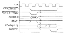
QCバス204に関しては、EPSM210は、データ信号PDATA[15:0]を通じて、QCデバイス202のレジスタおよびカウンタ306、310とデータの読み書きを行う。READ*信号は書き込み動作に対してはハイにアサートされ、読み出し動作に対してはローにアサートされる。QCデバイス202内の特定のレジスタは、ADRS[5:0]信号にアサートされたアドレスによって決定される。アドレス・ストローブ信号ADRS_STROBE*がいくつかのチップ選択信号CHIP_SELECTm*の対応する1つとともにアサートされると、QCデバイス202はADRS信号をラッチする。信号名に付けられた小文字の“m”は、一般に1つの特定のタイプに属する複数の信号を意味する。例えば、6つの別々のCHIP_SELECT[5:0]*信号があり、その場合それぞれの信号は6つのQCデバイス202のそれぞれ1つに別個にアクセスするためのものである。信号PREADY*は、要求されたデータがラッチされるCLK信号の立ち上がり後のライト・サイクル中に、CLK信号の1サイクルに対してQCデバイス202によってローにアサートされる。リード・サイクルについては、QCデバイス202が、データをPDATAバス上に置いた後の1CLKサイクルに対してPREADY*をローにアサートする。
【0031】
図5は、QCデバイス202のプロセッサ・リード・サイクルを図解する例示的なタイミング図であり、図6は、プロセッサ・ライト・サイクルを図解する例示的なタイミング図である。図7は、QCデバイス202のプロセッサ・バースト・リード・アクセス・サイクルを図解する例示的なタイミング図である。これらのタイミング図はいずれもあくまで例示であって、特定のタイミングや特定の信号特性などを示すものではなく、一般的な相関性を図解するものである。
【0032】
図4に戻り、これを参照する。ネットワーク・インタフェース信号は、負および正の衝突スレッショルド信号、衝突参照信号、信号中のシリアル・データ、負および正のマンチェスタ符号化データ信号、正および負のデータ・スレッショルド信号、データ・スレッショルド参照信号、正および負のプリエンファシス(Pre-emphasis)信号、および各QCデバイス202の[3:0]で表される4ポートの各々に対するよった対/AUIモード選択信号を含む。各QCデバイスはCLK信号を受信し、ポート104が使用する80、20および10MHzの内部クロック信号を生成するための20MHzのクロック信号を受信するCLOCK_20MHZ入力を有する。各イーサネット・コア300は、対応するセグメント108で発生する衝突を検知し、イーサネットのCSMA/CD(キャリア検知多重アクセス/衝突検出(Carrier Sense Multiple Access/Collision Detect))法に従ってジャミング・シーケンスを送信する。
【0033】
HSB206に関連するバス・インタフェース信号については、QCデバイス202がABORT_OUT*信号をアサートして1つのパケット全体をアボートする。EPSM210は、アボート信号ABORT_IN*をアサートして現在のバス・サイクルをアボートする。1つの実施例においては、QCデバイス202は、EPSM210がHSB206上で背圧サイクルを実行することによって受信しているパケットをアボートできるように考案されたQE110デバイスである。この特定のタイプの背圧機能は、1つのポートで受信中の1つのパケットの拒否を可能とする「パケット毎(パケット・バイ・パケット)」あるいは動的な「ポートごと」の背圧である。L64381デバイスは、本明細書で後に詳述する自動挿入フレーム・チェック・シーケンス信号(AI_FCS_IN*)を含む。QE110デバイスはAI_FCS_IN*信号を信号FBPN*と置換する。この信号はAI_FCS_IN*信号と同じ機能を遂行するために使用されるが、背圧サイクルおよびエンハンスト・パケット・フラッシュ(enhanced packet flush)を示すためにも用いられる。本明細書で説明しているように、動的背圧を実施するために使用できる代替方法が多数存在することは言うまでもない。特に、EPSM210は、背圧要求サイクルを実行するためにリード・サイクル中にFBPN*信号をアサートする。もしABORT_OUT*信号がリード・サイクルのデータ・フェーズの間に対応するQCデバイス202によってアサートされると、その背圧「要求」はそのQCデバイス202に認められたことになり、これがジャミング・シーケンスをアサートしてそのパケットをアボートする。もしABORT_OUT*信号がアサートされないと、EPSM210はそのパケットをドロップする。
【0034】
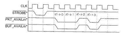
EPSM210は、QCデバイス202およびTPI220のすべてに対して状態ストローブ信号STROBE*をアサートし、その各々は、STROBE*信号がCLK信号の立ち上がりでアサートされてサンプリングされるときに、信号PKT_AVAILm*およびBUF_AVAILm*上で多重化された様式でその4つのポート104又は110(TPI220の場合)の状態で応答する。或る動作に対しては別のポートとして働く、各QCデバイス202に対する別個の信号、TPI220に対して1組及びCPU230に対して類似の組、がある。特にPKT_AVAILm*およびBUF_AVAILm*信号は、QCデバイス202用に信号PKT_AVAIL[5:0]*およびBUF_AVAIL[5:0]*と、TPI220用にそれぞれPKT_AVAIL[6]*およびBUF_AVAIL[6]*とも呼ばれる信号TPI_PKT_AVAIL*およびTPI_BUF_AVAIL*と、CPU230に対応するPKT_AVAIL[7]*およびBUF_AVAIL[7]*ともそれぞれ呼ばれる信号PCB_PKT_AVAIL*およびPCB_BUF_AVAIL*との、1つの信号タイプについて全部で8つの信号を含む。
【0035】
このように、HSB206は最初QCデバイス202が4つのポート、ポート0〜ポート3にアクセスするための信号PKT_AVAIL[0]*およびBUF_AVAIL[0]*を含み、HSB206は次のQCデバイス202が次の4つのポート、ポート4〜ポート7にアクセスするための信号PKT_AVAIL[1]*およびBUF_AVAIL[1]*を含み、と以下同様で、TPI220はポート、ポート24〜ポート27にアクセスするための信号PKT_AVAIL[6]*およびBUF_AVAIL[6]*を含み、EPSM210はCPU230に対する内部信号PKT_AVAIL[7]*およびBUF_AVAIL[7]*を含む。CLK信号のそれぞれのサイクルで分離される4つのポートに対応する各信号に、最高4ビットが多重化される。
【0036】
STROBE*信号に応答して、バス・インタフェース・ロジック308は、それぞれのポートに対する対応する各送信FIFO304にデータを格納するスペースが十分あるかどうかを表示するBUF_AVAIL[5:0]*信号のそれぞれのものに4つの状態ビットを多重化するためのポート状態ロジック303を含む。ポート状態ロジック303は、図示されている4つのポートのすべてに対して集中化するか、又はポート間に分散するかの何れかである。空きスペースの判定は、CPU230によって16、32あるいは64バイトにコンフィギュレーションされるのが望ましい、バス転送フィールド・サイズ(TBUS)を格納するバス・インタフェース・ロジック308内のコンフィギュレーション・レジスタに従う。同様に、STROBE*信号に応答して、TPI220は、後述するその内部の送信FIFOのそれぞれに、ポート24〜ポート27の各々に対するTLAN226の対応するものに対するデータを格納するスペースが十分あるかどうかを示すために、BUF_AVAIL[6]*信号に4つの状態ビットを多重化するための、HSB206に結合している類似したポート状態ロジック820(図31)を含む。CPU230あるいはポート28については、EPSM210内のPCB406(図11)が、EPSM210の内部の内部PCB送信FIFOにCPU230に対するデータを格納するための使用可能なスペースがあるかどうかを表示するためにBUF_AVAIL[7]*信号に1つの状態ビットをアサートする。
【0037】
同様に、STROBE*信号に応答して、各QCデバイス202内のバス・インタフェース・ロジック308のポート状態ロジック303は、それぞれのポートに対するその受信FIFO302の各々に、HSB206上におけるバス転送のための受信したデータを送信するために十分なデータがあるかどうかをTBUSの値によって表示するPKT_AVAIL[5:0]*信号のそれぞれのものに4つの状態ビットを多重化する。同様に、TPI220は、その内部の受信FIFOがHSB206上における転送のためにそれぞれのポート23〜ポート27から十分なデータを受信したかどうかを表示するPKT_AVAIL[6]*信号に4つの状態ビットを多重化する。CPU230については、EPSM210内のPCB406が、EPSM210の内部PCB受信FIFOがHSB206バス転送のためにCPU230から十分なデータを受信したかどうかを表示するPKT_AVAIL[7]*信号に1つの状態ビットをアサートする。
【0038】
図8は、QCデバイス202およびTPI220のバッファ状態問い合わせを図解する例示的なタイミング図であり、EPSM210によるSTROBE*信号のアサートと各QCデバイス202の応答、TPI220のアサートするそれぞれのPKT_AVAILm*およびBUF_AVAILm*信号をを含む。図8におけるポート0、ポート1、ポート2、およびポート3は、特定のQCデバイス202の4つのそれぞれのポートあるいはTPI220である。PCB406は、そのポートが4つのフェーズすべてでアクティブになっていることを除けば、その応答は同様である。STROBE*信号はレベル・トリガされ、従ってCLK信号の最初の立ち上がりでローにサンプリングされる。ここで、図8のタイミング図はあくまでも例示であって、特定のタイミングや特定の信号特性などではなく、一般的な相関性を図解するものであることに留意されたい。例えば、STROBE*信号は周期的であり、示した実施例の動作においては典型的には1CLKサイクルを超える間ローにアサートされる。
【0039】
図4に戻り、これを参照する。信号PORT_BUSY*は、それぞれのポートが半二重モードで送信中であるか受信中であるか、あるいはそのポートがいつ全二重モードで送信しているかを表示するために使用される。リード・データ信号READ_OUT_PKT[5:0]*はEPSM210にアサートされて、それぞれのQCデバイス202に対し、それぞれの受信FIFO302からのデータをデータ信号DATA[31:0]上に置くことを通知する。同様にして、ライト・データ信号WRITE_IN_PKT[5:0]*はEPSM210にアサートされて、それぞれのQCデバイス202に対し、データ信号DATA[31:0]からそれぞれの送信FIFO304にデータを取り出すことを通知する。さらに、類似の信号PCB_RD_OUT_PKT*、PCB_WR_IN_PKT*、およびTPI_READ_OUT_PKT*、TPI_WRITE_IN_PKT*がそれぞれTPI220およびCPU230用に含まれる。すべてのリードおよびライト信号は、集合的にそれぞれREAD_OUT_PKTm*およびWRITE_IN_PKTm*信号と呼称する。PORT_NO[1:0]ビットは、どの特定のポート104がHSB206上で実行されるサイクルに対してアドレスされているかを表示する。
【0040】
信号SOP*は、パケットの先頭又はヘッダがHSB206上に転送されたときにパケットの開始(Start Of Packet)を示す。AI_FCS_IN*信号は、一般にSOP*およびWRITE_IN_PKTm*信号の1つとともに外部のデバイスにアサートされ、
これにより、(QCデバイス202の1つの実施に対して)L64381デバイスが自動的にパケット内のデータからCRC(巡回冗長検査(Cyclic Redundancy Check))値を計算し、そのCRCをパケットのFCSフィールドに挿入するようにする。QE110デバイスは付加的な機能のために、前述したように、AI_FCS_IN*信号をFBPN*信号と置換する。EOP*信号は、HSB206上でデータ・パケットの最後のデータ転送が転送されたときにパケットの終了(End Of Packet)を表示する。BYTE_VALID[3:0]*信号は、DATA(データ)信号上の現在のワードにおいてどのバイトが有効であるかを表示する。通常1つのデータ・パケットはHSB206上での1回での転送には大き過ぎ、従って各バス・サイクルではTBUS値に等しいか又はこれより少ない量のデータが転送されることに留意されたい。
【0041】
各QCデバイス202が4つのポートのそれぞれを10Base−Tイーサネット・ポートとして動作させる点が理解できる。また、EPSM210がQCバス204を介してQCデバイス202のすべてのレジスタに読み書きのアクセスができるということが理解できる。さらに、EPSM210はHSB206を介して受信FIFO302のすべてからデータを読み取り、送信FIFO304のすべてにデータを書き込む。
【0042】
図9は、HSB206上での同時リード及びライト・サイクルを図解する例示的なタイミング図である。このタイミング図の一番上にサイクルのタイプを示しており、2つの同時リード及びライト・サイクルが順次実行される。CLK、CLK_2、STROBE*、READ_OUT_PKTm*、WRITE_IN_PKTm*、PORT_NO[1:0]、DATA[31:0]、およびABORT_OUT*信号をこのタイミング図のY軸(すなわち縦軸)に書いて示し、それに対して時間をX軸(すなわち横軸)に書いている。同時リード及びライト・サイクルには2種類があって、それらは特定の構成に依存して実行される。最初の一般的なタイプの同時サイクルについて、QCデバイス202がラッチ324および326を含むQE110デバイスで実施される場合は、なんら追加的な策を要せず同時リード及びライト・サイクルが実行される。これに代わって、もしQCデバイス202がL64381デバイスで実施される場合、外部のラッチおよび選択ロジック(示さず)が追加され、PORT_NO信号がHSB206上でアサートされたとき、これをラッチする。2番目の特殊なタイプの同時リード及びライト・サイクルは、何も補強せずL64381デバイスで実行される。ただし、それはPORT_NO信号が同じであるときのみ且つQCデバイス202が異なるときのみに限られる。
【0043】
EPSM210は、例えばリード、ライト、同時リード及びライト、背圧などといった、実行すべきサイクルのタイプを決定する。リード・サイクルは一般にREAD_OUT_PKTm*信号の1つのアサートによって指示され、ライト・サイクルは通常WRITE_IN_PKTm*信号の1つのアサートによって指示される。同時リード及びライト・サイクルは、READ_OUT_PKTm*信号とWRITE_IN_PKTm*信号の同時のアサートによって指示される。EPSM210は、例えば、後に詳述するように両ポートともカットスルー(CT)モードで動作すべくコンフィギュレーションされている場合のみのような、特定の条件の下で2つのポート間で同時リード及びライトを行う。
【0044】
同時サイクルの期間中、EPSM210は3番目のCLKサイクルの始まりでREAD_OUT_PKTm*信号の1つをローにアサートしてQCデバイス202の1つまたはTPI220を指示し、3番目のCLKサイクル中にPORT_NO[1:0]信号上に当該のポート番号をアサートして、アサートされた特定のREAD_OUT_PKTm*信号で識別されるQCデバイス202の4ポートのうちの1つを指示する。特定のREAD_OUT_PKTm*信号で識別されるQCデバイス202は、3番目のCLKサイクルにおいてPORT_NO[1:0]信号をラッチし、読み出される特定のポートを判断する。例えば、QCデバイス202を実施するQE110デバイスは、PORT_NO[1:0]信号をラッチするリード・ラッチ324を用いて構成される。また、TPI220は同様のリード・ラッチ819b(図31)を含み、これは、もしREAD_OUT_PKT[6]*信号で指示されていれば、3番目のCLKサイクルにおいてPORT_NO[1:0]信号をラッチする。あるいは、もしQCデバイス202の機能遂行に用いられるデバイスがL64381デバイスであれば、外部のラッチがこの目的に使用される。この時点で、識別されたポート0〜ポート27の特定のポートがHSB206上でリード・サイクルのソース・ポートとして指示されている。
【0045】
EPSM210は、次に4番目のCLKサイクルの始めでWRITE_IN_PKTm*信号の1つをローにアサートして、QCデバイス202の同じ又は他のものまたはTPI220を指示し、4番目のCLKサイクル中にPORT_NO[1:0]信号上に適当なポート番号をアサートし、アサートされた特定のWRITE_IN_PKTm*信号で示されるデバイスの4ポートのうち1つを指示する。特定のWRITE_IN_PKTm*信号で識別されるQCデバイス202は、4番目のCLKサイクルにおいてPORT_NO[1:0]信号をラッチし、書き込まれる特定のポートを判断する。例えば、QCデバイス202の機能を実施するQE110デバイスは、第4のCLKサイクルにおいてPORT_NO[1:0]信号をラッチするためのライト・ラッチ326を用いて構成される。また、TPI220は、もしWRITE_IN_PKT[6]*信号で指示されたならば、4番目のCLKサイクルにおいてPORT_NO[1:0]信号をラッチするための同様のライト・ラッチ819bを含む。このようにして、ポート0〜ポート27の他のいずれかのポートがHSB206上のライト・サイクルの宛て先ポートとして指示され、そのライト・サイクルは指示されたばかりのリード・サイクルと同時に実行される。ソース・ポートと宛て先ポートは、同一のQCデバイス202上か、TPI220の2つのポート間か、異なるQCデバイス202間のいずれに存在し得る。しかし、示した実施例においては、同時リード及びライト・サイクルは、QCデバイス202のポート104の1つとTPI220のポート110の1つとの間では、データ転送の速度が違うために実行されない。
【0046】
CLK信号の次のサイクルで、パケット・データはHSB206を介して転送、あるいはソース・ポートから読み出され、直接に宛て先ポートに書き込まれ、その際EPSM210あるいはメモリ212には格納されない。データ転送は、実施例によって異なるが幾つかのバイトを転送するためにサイクル5、6、7、および8で実行される。例えば、L64381デバイスに関しては64バイトまでが転送され、QE110デバイスでは256バイトまでが転送される。データ転送に4つのCLKサイクルを示しているが、送るべきデータの量によっては1、2あるいは4のCLKサイクルで転送される場合もあり得る。新しパケットに関しては、最初に通常のリード・サイクルが実行されてソースおよび宛て先のMACアドレスがEPSM210に供給され、これが後に詳述するハッシュ手順を実行し、もし既知であれば、宛て先ポート番号を決定する。受信先(宛て先)ポート番号が分かり、そしてもし宛て先ポートが1つだけであれば、必要に応じてパケットの残存部分のいずれかの部分あるいは全部について、同時リード及びライト動作を実行することができる。
【0047】
もしPORT_NO信号が同じであるが、2つの異なったポート間であり、従って2つの異なったQCデバイス202間であるならば、特殊なタイプの同時リード及びライト・サイクルが実行される。図9ではこのケースも図解しているが、サイクル全体を通してPORT_NO信号が不変のままであるという点が例外である。PORT_NO信号が変わらないので、ラッチ324、326は不要である。従って、このタイプの同時サイクルは2つの異なるL64381デバイス間で、外部にラッチや選択ロジックを必要とせずに実行することができる。EPSM210は、送信元(ソース)と宛て先のポート間でPORT_NO信号が等しいこと、および2つの異なったQCデバイス202が用いられることを判断してから、説明したように同時サイクルを実行する。
【0048】
図9に図解されているように、2回目の同時リード及びライト転送は6番目のCLKサイクルで発生し、PORT_NO[1:0]信号が7番目、8番目および9番目のサイクルにおいて、それぞれ、リード・モード、リード・ポート番号、およびライト・ポート番号でアサートされる。それに応答して、READ_OUT_PKTm*信号は7番目のCLKサイクルに対してデアサート(de-assert)される。同様に、WRITE_IN_PKTm*信号は8番目のCLKサイクルに対してデアサートされる。この2回目の同時サイクルは、同一データ・パケットの続きのない連続したデータを供給するための最初の同時サイクルの続きか、あるいはまったく異なったデータ・パケットの開始のいずれかである。同一パケットの連続したデータについては、ソースおよび宛て先のポートは同じである。しかし、ソース・ポートまたは宛て先ポートあるいはその両方は、異なるパケットのデータを転送する2回目の同時サイクルでは同一のものではないこともある。
【0049】
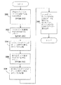
図10は、HSB206上で同時リード及びライト・サイクルを実行する手順を示すフローチャートである。最初のステップ330で、EPSM210は、ソース・ポートと宛て先ポートの間でのHSB206上での同時リード及びライト・サイクルが実行可能かどうかを判断する。EPSM210は、それから次のステップ332で、ソース・ポートを識別するための適当な信号をアサートする。これは、HSB206上でPORT_NO信号を用いてソースまたは「リード」ポートの番号をアサートすることによって、及び適当なREAD_OUT_PKTm*信号をアサートすることによって行われる。次のステップ334では、識別されたソース・ポート・デバイスがその識別(アイデンティフィケーション)信号を検知もしくは格納する。ラッチを伴わない特殊な同時サイクルでは、QCデバイス202がHSB206上でREAD_OUT_PKTm*信号を検知し、続いてPORT_NO信号を検知して、リード・サイクルの準備を開始する。ラッチを用いる一般的な同時サイクルでは、指示されたQCデバイス202あるいはTPI220がステップ334でリード・ポート番号をラッチし、リード・サイクルの準備を開始する。
【0050】
次のステップ336では、EPSM210は宛て先ポートを識別するための適当な信号をアサートする。特殊な同時サイクルでは、EPSM210は適当なWRITE_IN_PKTm*信号をアサートし、同じPORT_NO信号を維持する。一般の場合では、ステップ336において、EPSM210はまた、HSB206上に宛て先または「ライト」ポート番号を適当なWRITE_IN_PKTm*信号とともにアサートする。続くステップ338では、識別された宛て先ポート・デバイスがその識別信号を検知もしくは格納する。ラッチを伴わない特殊な同時サイクルでは、示されたQCデバイス202がHSB206上でWRITE_IN_PKTm*信号を検知し、続いてPORT_NO信号を検知して、ライト・サイクルの準備を開始する。一般的な場合では、指示されたQCデバイス202あるいはTPI220が、ステップ338、で宛て先またはライト・ポート番号をラッチする。最後に、同時リード及びライト・サイクルのステップ340で、ここで指示されたソース・ポートがHSB206上にデータを送出し、指示された宛て先ポートがHSB206からデータを読み取る。
【0051】
同時リード及びライト動作は、パケット・データの各転送にただ1つのバスしか必要としないため、最速タイプのデータ転送サイクルである。後に詳述するように、通常のCTモードの動作では少なくとも2回の転送が必要である。すなわち、1つはソース・ポートからEPSM210へ、そしてもう1つはEPSM210から宛て先ポートへの転送であって、これは同じデータに対してHSB206上で2つの別のサイクルが必要となる。同時リード及びライト・サイクルは、HSB206上で同一のデータについて1回で直接の転送を要し、それによりHSB206の帯域幅が増大する。その他、幾つかの暫定的なCTや蓄積転送(SnF)モードを含むより遅いモードもあり、その場合、パケット・データはメモリ212に書き込まれてから宛て先ポートに転送される。
【0052】
次に図11を参照すると、EPSM210の簡略なブロック図で、データの流れとコンフィギュレーション・レジスタを図解している。EPSM210は、HSBコントローラ・ブロック(HCB)402、メモリ・コントローラ・ブロック(MCB)404、およびプロセッサ制御ブロック(PCB)406という3つの主要セクションを含む。QCインタフェース410はHSB206をEPSM210のHCB402に結合する。QCインタフェース410の他側には1組のバッファ、すなわちFIFO412が結合されており、これらのFIFO412には受信FIFO、送信FIFO、および本明細書で後に詳述するカットスルーFIFOが含まれる。FIFO412の他側(図12のCTバッファ528を除く)は、MCBインタフェース414を介してMCB404に結合されており、そのMCBインタフェース414は適当なバス420を介してMCB404内のHCBインタフェース418に結合されている。HCBインタフェース418はさらにメモリ・インタフェース422に結合され、メモリ・インタフェース422はメモリ・バス214を介してメモリ212に結合される。メモリ・インタフェース422はさらにPCBインタフェース424の一側に結合されており、そのPCBインタフェース424の他側は適当なMCBバス428を介してPCB406内のMCBインタフェース426の一側に結合されている。MCBインタフェース426の他側は1組のFIFO430の一側に結合されており、FIFO430がさらにPCB406内のCPUインタフェース432に結合されている。CPUインタフェース432はQC/CPUバス204およびCPUバス218に結合される。CPUインタフェース432はさらにPCB406内の第2の組のFIFO434の一側に結合されており、FIFO434の他側はQC/HCBインタフェース436に結合されている。QC/HCBインタフェース436の他側は適当なHCBバス438を介してQCインタフェース410に結合されている。
【0053】
PCB406とCPU230に関連するHCBバス438のPCB_BUF_AVAIL*、PCB_PKT_AVAIL*、PCB_RD_OUT_PKT*、およびPCB_WR_IN_PKT*信号は、それぞれ、BUF_AVAILm*、PKT_AVAILm*、READ_OUT_PKTm*、およびWRITE_IN_PKTm*信号に含まれていることに留意されたい。示した本実施例において、HCBバス438はHSB206と類似しており、本質的にはEPSM210内のHSB206の内部バージョンである。PCB406は、HCB402に対してポート104のそれぞれおよびTPI220と同様の働きをする。このようにして、CPU230はPCB406の動作を通じて、HCB402に対する追加的なポート(PORT28)として動作する。
【0054】
CPUインタフェース432はバス442を介してレジスタ・インタフェース440に結合され、レジスタ・インタフェース440はさらにレジスタ・バス444に結合される。レジスタ・バス444はHCB402内の1組のHCBコンフィギュレーション・レジスタ、およびMCB404内の1組のMCBコンフィギュレーション・レジスタ448に結合される。このようにして、CPU230は、CPUインタフェース432とレジスタ・インタフェース440を介し、HCBコンフィギュレーション・レジスタ446およびMCBコンフィギュレーション・レジスタ448の両方のレジスタの初期設定とプログラミングを行う。
【0055】
MCBコンフィギュレーション・レジスタ448は、ポートおよびメモリ212に関連する相当な量のコンフィギュレーション情報の格納に使用される。例えば、MCBコンフィギュレーション・レジスタ448は、各ポートが学習(LRN)状態か転送(FWD)状態かブロック(閉じた)(BLK)状態か聴取(LST)状態か又はディスエーブル(DIS)状態かを示すポート状態情報、メモリ・セクタ情報、メモリ・バス214のバス使用情報、ドロップされたパケットの数、ハッシュ・テーブル定義、メモリ・スレッショルド、BCスレッショルド、もしあれば機密保護ポートのアイデンティフィケーション、メモリ制御情報、MCB割り込みソース・ビット、割り込みマスクビット、ポーリング・ソース・ビットなどを含む。
【0056】
EPSM210の説明では、CPU230はコンフィギュレーションおよび制御の目的で、QCデバイス202およびメモリ212にアクセスできることを述べている。EPSM210とのHSB206を用いる主たるデータ・フローはFIFO412とメモリ212を通じてのものであるが、HSB206とCPU230との間でも、HCBバス438およびEPSM210の関連するFIFO及びインタフェースを介したデータ・フローも発生する。
【0057】
次に図12を参照すると、HCB402の詳細なブロック図が示されている。HCBバス438はPCB406にインタフェースするためのHSB206の内部バージョンであり、そこでバス206と438を一括してHSB206と呼称する。ポーリング・ロジック501は、HSB206、1組のローカル・レジスタ506、およびHCBコンフィギュレーション・レジスタ446に結合されている。ポーリング・ロジック501は、CLK信号を受信し、ポート104、110およびPCB406を問い合わせるべくQCデバイス202およびTPI220へのSTROBE*信号を周期的にアサートする。ポーリング・ロジック501は、QCデバイス202およびTPI220からの多重化されたPKT_AVAILm*およびBUF_AVAILm*信号をモニタする。ここで、各QCデバイス202およびTPI220は、前述したように、その4つのポート104、110の状態をそれぞれ供給する。TPI220はPKT_AVAIL[6]*およびBUF_AVAIL[6]*信号で応答し、PCB406はPKT_AVAIL[7]*およびBUF_AVAIL[7]*信号で応答する。
【0058】
ポーリング・ロジック501は受信(RX)ポーリング状態マシン502を含み、これでPKT_AVAILm*信号を見直し(リビューし、review)、レジスタ506内の受信リスト(RECEIVE LIST)509を更新する。同様に、ポーリング・ロジック501は送信(TX)ポーリング状態マシン503を含み、これでBUF_AVAILm*信号を見直し、レジスタ506内の送信リスト(TRANSMIT LIST)510を更新する。もしHCBコンフィギュレーション・レジスタ446におけるWTPRIORITYフラグがCPU230によってセットされれば、RXポーリング状態マシン502およびTXポーリング状態マシン503の両方は、HCBコンフィギュレーション・レジスタ446内の1組のウエイト・ファクタ(WEIGHT FACTORS)508使用して、後に詳述するように、それぞれ受信リスト509および送信リスト510をプログラミングする。HCBコンフィギュレーション・レジスタ446はまた1組のCT_SNFレジスタ507を含んでおり、これがCPU230にプログラミングされ、対応するポートがソース・ポートあるいは宛て先ポートである場合、所望される動作モードをCTとSnFとの間で決定する。
【0059】
レジスタ506は、ラッチ、フリップ・フロップ、スタティックRAM(SRAM)、DRAMデバイスなどのような、EPSM210の実施に従っての任意の様式で実施され、複数の状態および制御(コントロール)のレジスタ又はバッファを含む。受信リスト509は、各ポートの相対的受信状態(ステータス)および優先度(優先順位)を示す複数のレジスタ値を含む。同様に、送信リスト510は、各ポートの相対的送信ステータスおよび優先度を示す複数のレジスタ値を含む。PRカウント(RPCOUNT)・レジスタ511aは、各ポートが外部のネットワーク・デバイスからパケット・データを受信したとき、その受信ポートに相対的な受信優先順位を割り当てるためにRXポーリング状態マシン502によって使用されるPRカウント(RPCOUNT)番号を格納している。もしくは、RXポーリング状態マシン502はウエイト・ファクタ508からの対応するウエイト(重み)・ファクタを使用する。同様に、TPカウント(TPCOUNT)・レジスタ511bは、ポートによって外部のネットワーク・デバイスへ送信できるパケット・データがあり、ポートが送信のためのデータを収容可能なとき、そのポートに相対的な送信優先順位を割り当てるためにTXポーリング状態マシン503によって使用されるTPカウント(TPCOUNT)番号を格納する。もしくは、TXポーリング状態マシン502はウエイト・ファクタ508からの対応するウエイト・ファクタを使用する。相対的アービトレーション・カウント番号RXニューカウント(RXNEWCNT)、RXACTカウント(RXACTCNT)、TXニューカウント(TXNEWCNT)およびYXCTカウント(TXCTCNT)は、それぞれ、レジスタRXニューカウント511c、RXACTカウント511d、TXニューカウント511eおよびTXCTカウント511fに格納される。
【0060】
HCB402は、レジスタ506および446内のデータを調べてHSB206上で実行されたサイクルのタイプを判断するために結合されたアービトレーション・ロジック504を含む。HSBコントローラ505は、EPSM210とHSB206との間のデータ・フローをコントロールするために、HSB206上で実行される各サイクルを実行及び制御する。HSBコントローラ505は、状態ビットを変更するためにレジスタ506に結合される。HSBコントローラ505は、各サイクルのタイプのアイデンティフィケーションをアービトレーション・ロジック504から受け取る。アービトレーション・ロジック504は、新パケット受信(RX NW)アービタ513、受信アクティブ(RX ACT)アービタ514、新パケット送信(TX NW)アービタ515および送信カットスルー(TX CT)アービタ516の全部で4つのデータ・アービタに結合されたメイン(MAIN)・アービタ512を含む。メイン・アービタ512は、一般に、RX NWアービタ513、RX ACTアービタ514、TX NWアービタ515、およびTX CTアービタ516の間で選択を行い、各アービタは調停(仲裁)を行って次のサイクルを決める。メイン・アービタ512は、必要に応じて条件に適ったいずれかの優先順位スキームを用いる。例えば、示した実施例においては、メイン・アービタ512はラウンドロビン優先順位スキームを採用する。
【0061】
FIFO412は任意の望ましい様式で実施される。示した実施例においては、2つの受信バッファ、RX BUF520および522でRX FIFOを実現しており、データは1つのバッファへの書き込み中に他のバッファから読み出され、また、その逆も行われる。また、2つの送信バッファ、TX BUF524および526が用意されており、RX BUF520および522と同様に動作する。FIFO412は、少なくとも1つのカットスルー・バッファ、CT BUF528も含む。RX BUF520および522は両方とも64バイトのバッファであり、それぞれが両方向のデータ・フローを実現するためにHSB206との双方向データ・インタフェース、およびRX MCBインタフェース530を介してMCB404にデータを送るための単向インタフェースを含む。TX BUF524および526は両方とも64バイトのバッファであり、HSB206とTX MCBインタフェース531との間に結合されている。TX BUF524および526は、TX MCBインタフェース531を介してMCB404からデータを受け取り、データをHSB206に送る。CT BUF528は64バイトのバッファであり、HSB206との双方向インタフェースを有する。FIFOコントロール・ブロック529は、FIFO520、522、524、および526のデータ・フローを制御するため、及びRX MCBインタフェースおよびTX MCBインタフェース530、531を介してアサートされた特定の状態信号を検知するため、及び後に詳述するように、レジスタ506内の特定のビットをセットするために、レジスタ506、HSBコントローラ505、RX BUF520と522、TX BUF524と526、CT BUF528、RX MCBインタフェース530およびTX MCBインタフェース531に結合している。
【0062】
バス420は、RX MCBインタフェース530、TX MCBインタフェース531、ハッシュ要求ロジック(ハッシュ・リクエスト・ロジック)及びMCBインタフェース(HASH REQ LOGICと呼ぶ)532、および送信アービタ要求ロジック(TX ARBリクエスト・ロジック)及びMCBインタフェース(TX ARB REQ LOGICと呼ぶ)533を介してHCB402をMCB404にインタフェースするための複数のデータおよび制御信号を含む。HSBコントローラ505は、ポート0〜ポート28の1つからのそれぞれの新しいパケットのヘッダをRX BUF520と522の1つに、及びHASH REQ LOGIC532にコピーする。ヘッダは、サイズが少なくとも3つのDWORD(それぞれ32ビット)すなわち96ビットであり、ソースと宛て先の両方のMACアドレスを含む。HASH REQ LOGIC532は、MCB404によって実行されるハッシュの手順を要求し、適当なビットをレジスタ506にセットする。このハッシュ手順は、パケットに対して取られる適当な動作を決定するために行われる。
【0063】
示した実施例において、新しパケットのヘッダを受け取った後、HASH REQ LOGIC532はMCB404へ信号HASH_REQ*をアサートし、HASH_DA_SA[15:0]信号上に48ビットのMACの宛て先およびソース・アドレスおよび8ビットのソース・ポート番号を多重化する。MCB404はHASH_REQ*信号を検知し、ハッシュ手順を実行し、そしてHASH REQ LOGIC532へ信号HASH_DONE*をアサートする。MCB404は、状況が許せば、信号HASH_DSTPRT[4:0]、HASH_STATUS[1:0]、及びHASH_BP*もアサートする。HASH_STATUS[1:0]信号は次の4種類の結果の1つを表示する。すなわち、それらは、パケットをドロップするための00b=DROP_PKT(bは2進数を示す)、ブロードキャスト(同報通信)(BC)パケットに対しての01b=GROUP_BC、宛て先ポートが未知であり、従ってBCパケットであるという10b=MISS_BC、および単一の宛て先ポートへのユニキャスト・パケットを示す11b=FORWARD_PKTである。もしHASH_STATUS[1:0]=FORWARD_PKTであれば、HASH_DSTPRT[4:0]信号が、そのパケットの宛て先ポートを指定する2進数のポート番号とともにアサートされる。HASH_BP*信号は、もし背圧がイネーブルとなっていて適用可能であれば、MCB404が判断したメモリ212におけるスレッショルド・オーバーフロー状態に起因して、背圧を示すためにアサートされる。
【0064】
一定のしきい(スレッショルド)値が、メモリ212全体に対して、特定のタイプのパケット(例えばBCパケット)に対して、及びポートごとに設定される。しきい値に達したとき、従ってメモリ212にもう1つのパケットを入れるとスレッショルド条件を侵すことになる場合、そのパケットのドロップの如何はネットワーク・スイッチ102が決定する。送信側のデバイスは最終的にそのパケットがドロップされたことを検知し、そのパケットを再送信する。或るスレッショルド条件に違反があった場合、もし背圧がイネーブルとなっていてソース・ポートが半二重モードで動作していれば、HASH_BP*信号がアサートされる。
【0065】
HASH REQ LOGIC532はHASH_BP*信号を検知して、例えばソース・ポートと宛て先ポートが同じかのように、HASH_STATUS[1:0]=DROP_PKTであるかどうかを判断する。もしHASH_STATUS[1:0]=DROP_PKTであれば、そのパケットはドロップされるべきものであるから、それ以上の動作は不要である。もしHASH_STATUS[1:0]とDROP_PKTが等しくなければ、HASH REQ LOGIC532はHASH_STATUS[1:0]=FORWARD_PKTであるかどうかを判断し、そのパケットはCT BUF528を介してCTモードで転送されることになり、可能性としてメモリ212が避けられる。もし宛て先ポートが使用中(ビジー)であるか、またはもしHASH_STATUS[1:0]がパケットのドロップあるいは転送を指示しなければ、HASH REQ LOGIC532が、データを受信するポートに対して背圧サイクルを実行するようHSBコントローラ505に指示する。
【0066】
SnF動作の間、EPSM210は、パケットのいずれかの部分を宛て先ポートへ送信する前に、パケット全体を受信してメモリ212に格納する。パケットの受信が完了後であって、もし宛て先ポートが既知であれば、そのパケットは、使用されている特定のアービトレーション・スキームに従って、可能なときに宛て先ポートに送られる。CT動作を適用する場合、両方のポートがCT_SNFレジスタ507内でCTモードにプリセットされ、両ポートが同一速度で動作し、そして宛て先ポートのTBUS設定がソース・ポートのTBUS設定と比べて等しい又は大きい。100Mbpsのイーサネット・ポート、ポート24〜ポート27の実現にTLAN226を使用するここに示した特定の実施例において、TLANは送信に先立ってパケット全体のサイズが必要であるため、ポート24〜ポート27についてCTモードは実行されない。また、示した実施例ではTBUSの値が等しいことが要件である。本発明は、これら様々な設計上の問題には制約されない。CTモードでの動作中、EPSM210は指示された宛て先ポートに対して、もしこれがビジーでなければ、データを送信するために、データを適当なQCデバイス202に供給する。パケット・データはメモリ212には転送されず、ソース・ポートと宛て先ポートの間のFIFO412を通じて緩衝格納(バッファ記憶)される。
【0067】
もし受信したパケットの先頭で受信先のポートがビジーであれば、データは暫定的(interim)CT動作モードに従って、ソース・ポートと宛て先ポートの間のメモリ212内でバッファされる。しかし、パケット部は宛て先ポートによる送信に直ちに使用可能であって、宛て先ポートへの転送に、パケット全体の受け取り完了を待つ必要がない。安全対策として、暫定的CT動作モードを無効とし、その特定のパケットのための動作を次のパケットのSnFモードに切り替えるメカニズムが適用できる。
【0068】
CTモードでのパケット転送中に、例えば宛て先ポートの停止のような何らかの理由で宛て先ポートがそれ以上のデータの受信をできなくなった場合、動作はミッドパケット(mid-packet)暫定CTモードに切り替えられる。ミッドパケット暫定CTモードの間、FIFO412内のパケット・データはメモリ212へ送られ、その後宛て先ポートがさらにデータを受信することができるときにパケット・データがそのポートに送られる。他の後続の受信されたパケットが、同じ停止したポートによる送信のために他のポートによって受信され、これら後続のパケットはそのポートに対する対応する送信チェーン内に入れられるので、ミッドパケット暫定CTモードに切り替えられたパケットの残りの部分は順序の適性化を意図してその送信チェーンの先頭に置かれることに留意されたい。
【0069】
もう1つのモードは適応(アダプティブ)SnFモードと呼ばれる。パケットがCT動作モードで転送されている間、CPU230は、ポート104、110、およびPCB406のいずれか1つまたはそれ以上に「ラント(runt)」、「オーバーラン」、「ジャバー(jabber)」、遅刻衝突(レイト・コリージョン、late collision)、FCSエラーなどの誤りが相当回数発生するかどうかを判定するために、それらのアクティビティの監視及び追跡を行っている。ラントはデータが一定の最少量に満たないパケットで、示した本実施例におけるその最小サイズは64バイトである。オーバーランはデータが一定の最多量より多いパケットで、イーサネット標準に従って示されている本実施例におけるその最大サイズは1518バイトである。ジャバーはサイズが最大サイズ(イーサネットではの1518バイト)を超えており、無効なCRC(巡回冗長検査、(Cyclic Redundancy Check))値が入っているパケットである。通常、このような誤りのあるパケットはドロップされ、システム内に伝播されることはない。適応SnFモードについては、もしポート104がCTモードで動作していて、このような誤りの発生がCPU230が判断するところでは頻繁であると、CPU230は誤りが訂正または除去されるまで、そのポートにプリセットされているモードをCT動作からSnF動作に切り替える。各TLAN226のポート110の動作も同様であるが、パケット・データがTPI220を通じてHSB206を介してEPSM210に入り、送信の前にメモリ212に格納されるという点が異なる。TPI220は、実際上PCIバス222とHSB206との間のブリッジとして動作する。TLAN226が外部のネットワークにパケットを送信する前にはパケット全体の長さが必要であり、従って、各パケットはTLAN226の1つによって再送信される前に、そのパケットが受信されてその全体がメモリ212に格納される。さらに、QCデバイス202による送信用にTLAN226が受け取るデータ、およびTLAN226による送信のためにQCデバイス202が受け取るデータは、示した実施例におけるデバイス202と226の間の速度の差が大きいため、SnFモードで処理されてメモリ212に格納される。
【0070】
RX MCBインタフェース530は、パケット・データがRX BUF520、522の1つに入っていてメモリ212への転送準備完了状態にあるとき、MCB404へRX_PKT_AVAIL*信号をアサートする。パケット・データはHCB402から転送され、メモリ・データ出力バスMemDataOutあるいはMDO[31:0]を介してMCB404へ転送される。スタティック信号MEM_EDOは、メモリ212のタイプがEDOか同期DRAMであればアサートされ、FPM DRAMであればアサートされない。RX MCBインタフェース530は、RX_PKT_AVAIL*信号を適宜にアサートしている間、他のいくつかの信号もアサートする。特に、RX MCBインタフェース530は、1CLKサイクルに対してRX_SRC_DST[4:0]信号上にソース・ポート番号を多重化し、続いて、RX_PKT_AVAIL*信号をアサートしているときに、次のCLKサイクルの間に、もし既知であれば、宛て先ポート番号を多重化する。また、RX MCBインタフェース530は、選択されたRX BUF520、522内の、信号RX_CNT[5:0]上のDWORDの数(マイナス1DWORD)をアサートする。
【0071】
RX MCBインタフェース530は、もしデータがパケットの始まりであれば信号RX_SOP*をRX_PKT_AVAIL*信号とともにアサートし、もしデータがそのパケットの終わりであれば信号RX_EOP*をRX_PKT_AVAIL*信号とともにアサートする。RX MCBインタフェース530は、パケットがCTモードで転送中であるが、暫定CTやミッドパケットCTモードの場合のようにメモリ212で緩衝格納されていれば、信号RX_CUT_THRU_SOP*を信号RX_PKT_AVAIL*およびRX_SOP*とともにアサートする。特に、もし(!RX_CUT_THRU_SOP* & !RX_PKT_AVAIL* & !RX_SOP*)であれば暫定CT(全パケット)が指示され、もし(!RX_CUT_THRU_SOP* & !RX_PKT_AVAIL* & RX_SOP*)であれば暫定CTミッドパケットが指示される。RX MCBインタフェース530は、もし宛て先アドレスが未知であり、そしてパケットがBCパケットであれば、信号RX_MISS_BC*をRX_PKT_AVAIL*およびRX_SOP*信号とともにアサートする。RX MCBインタフェース530は、もしヘッダ内でGROUP(グループ)ビットがセットされていれば、従って、また。パケットがBCパケットであれば、信号RX_GROUP_BC*をRX_PKT_AVAIL*およびRX_SOP*信号とともにアサートする。RX MCBインタフェース530は、信号RX_END_BYTE[1:0]をRX_PKT_AVAIL*およびRX_EOP*信号とともにアサートし、パケット内の最終バイトのバイト・レーン(lane)を示す。
【0072】
RX MCBインタフェース530は、ソース・ポートが送信中にABORT_OUT*信号をアサートしてパケット内における誤りの検知と表示を行えば、信号RX_ERROR*をRX_PKT_AVAIL*およびRX_EOP*信号とともにアサートする。FIFOオーバーラン、ラント・パケット、オーバーサイズのパケット、フレーム・チェック・シーケンス(FCS)・エラー、あるいはフェーズ・ロックト・ループ(PLL)エラーの検知のように、各種のエラー状況がポート104、110によってチェックされる。もしRX_ERROR*信号がアサートされると、ネットワーク・スイッチ102は、パケットがSnFモードで転送中であれば、そのパケットをドロップする。
【0073】
MCB404は、アサートされたRX_PKT_AVAIL*信号を検知した後、そして前述のようにRX_PKT_AVAIL*信号でアサートされた関連の信号をラッチした後に、HCB402へのRX_ACK*信号をアサートする。MCB404は、次のDWORDのデータを受け取れる状態に入ったときRX_STB*信号をアサートする。MCB404は、HCB402がデータを要求する可能性があると判断したとき、信号RX_PKT_COMPLETE*をアサートする。とりわけMCB404は、CTモードのパケットに対してHCB402によってアサートされたRX_SOP*信号を検知した後にRX_PKT_COMPLETE*信号をアサートする。またMCB404は、SnFモードのパケットに対してHCB402によってアサートされたRX_EOP*信号を検知した後にRX_PKT_COMPLETE*信号をアサートする。MCB404は、SnFパケットに関してRX_ERROR*信号がアサートされていた場合(RX_SOP*信号とともにアサートされていないRX_CUT_THRU*信号で示される状態)には、RX_PKT_COMPLETE*信号をアサートしない。MCB404は、MCB404が判断したメモリ212におけるオーバーフロー状態に起因してパケットがドロップされた場合、RX_PKT_COMPLETE*信号の代わりにHCB402へ信号RX_PKT_ABORTED*をアサートする。
【0074】
TX ARB REQ LOGIC533は、使用可能な宛て先ポートによる送信のためのデータのメモリ212からの取り出し要求を、アービトレーション・ロジック504から受け取る。この要求は、一般にTX NWアービタ515から出される。TX ARB REQ LOGIC533は、応答してMCB404へ送信要求信号TX_ARB_REQ*をアサートし、一方、信号TX_ARB_PORT[4:0]上に宛て先ポート番号を、及び信号TX_ARB_XSIZE[2:0]に各データ部の最大転送長をアサートする。TX BUF524および526について、最大転送長は、000b=16バイト、001b=32バイト、010b=64バイト、011=128バイト、および100=256バイトとして定義される。MCB404はこれらの値をラッチし、TX ARB REQ LOGIC533へ肯定応答(アクノレッジ)信号TX_ARB_ACK*をアサートする。MCB404は、要求されたデータをメモリ212から取り出し、そのデータをTX BUF524、526の1つに書き込む。
【0075】
データはメモリ・データ入力バスMemDataInまたはMDI[31:0]を介してHCB 402内のTX BUF 524、526へ転送される。TXMCBインタフェース531は、TX BUF 524および526のいずれかがMCB404からのデータの受け取りに使用可能であるとFIFO制御ブロック529が判断したとき、TX_BUF_AVAIL*をアサートする。MCB404は、使用可能なTX BUF 524あるいは526に格納すべくHCB402のTX MCBインタフェース531によるサンプリングの対象となるデータが存在するとき、ストローブ信号TX_STB*をアサートする。MCB404は、データの特性を識別するためにTX_STB*と同時にいくつかの信号もアサートする。特に、MCB404はTX_STB*信号とともに信号TX_SOP*をアサートし、メモリ212からデータの始めを検出する。MCB404はTX_STB*信号とともにTX_AIFCS*信号をアサートし、送信元ポートがCPU 230を指示しているPCB406であるかどうかを判断する。MCB404はTX_STB*信号とともに信号TX_CNT[5:0]上の2進数をアサートする。ここで、TX_CNT[5:0]は選択したTX FIFOに書き込むDWORDの数(マイナス1DWORD)を表す。MCB404はTX_STB*信号とともに信号TX_EOP*をアサートし、メモリ212からパケットの終わりを検出する。MCB 404はTX_EOP*およびTX_STB*信号とともにバッファ・チェーン終結信号TX_EOBCもアサートし、メモリ212内に特定の受信先ポートに宛てたデータが無くなったかどうかを確認する。MCB 404はTX_EOP*およびTX_STB*信号とともにエンド・バイト信号もアサートしてパケット内の最終バイトのバイト・レーンを示す。
【0076】
BCパケットについては、MCB404がMDI[31:0]信号上のBCビットマップをアサートしつつ信号BC_PORT_STB*をアサートする。FIFO制御ブロック529は、BC_PORT_STB*信号がアサートされたことを検知し、MDI[31:0]信号をラッチして結果を内部のBCBITMAP[28:0]レジスタ内に格納する。FIFO制御ブロック529は、TRANSMIT LIST 510内のメモリ・ビット配列TXMEMCYC[28:0]のビットを設定するときにBCBITMAPレジスタ内の値を用いる。
【0077】
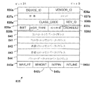
図13は、レジスタ506に属するいくつかのレジスタの図解である。CT_SNFレジスタ507は、プログラミング可能な送信元ポート・モードのビット配列SRC CT_SNF[28:0]を含み、各ビットはそれぞれポートPORT28からPORT0の1つに対応しており、対応するポートが送信元ポートである場合にCTとSnF間における動作モードを指定するためCPU 230によってプログラミングされる。特に、特定のポートにSRC CT_SNFビットがセットされている場合、そのポートが送信元ポートとして機能するときの動作モードとしてはCTモードが望ましい。SRC CT_SNFビットがクリアされている場合は、そのポートが送信元ポートとして機能するときの動作モードとしてはSnFモードが望ましい。同様に、CT_SNFレジスタ507は、プログラミング可能な受信先ポート・モードのビット配列DEST_CT_SNF[28:0]を含み、各ビットはそれぞれポートPORT28からPORT0の1つに対応しており、対応するポートがユニキャスト用の受信先ポートである場合にCTとSnF間における動作モードを指定するためCPU230によってプログラミングされる。CTモードは、送信元と受信先の両方のポートがCT_SNFレジスタ507でCTモードに指定されている場合にのみ望ましい。
【0078】
RECEIVE LIST 509は、対応する受信優先権カウントを格納する複数のレジスタを含む。優先権カウントはRXPORTBUFx[4:0]カウントと呼ばれ、“x”はポート番号である。最高32のポートに優先権を割り当てるために、示した実施例においては各RXPORTBUFx[4:0]カウントは5ビットである。RECEIVE LIST 509は対応するポート・マスクビット配列RXPRTMSK[28:0]を含み、それぞれのRXPRTMSKビットは初めにロジック0、すなわち優先権がまだ割り当てられていないとき、そしてそれぞれのPKT_AVAILm*信号がその後アサートされたときにRXポーリング・ステート・マシン502によってセットされる。そのとき、RXポーリング状態マシン502は対応するRXPORTBUFxレジスタ内に優先権番号を割り当てる。割り当てられた優先権番号は、そのポートがサービスされるまで有効となっている。RXPRTMSKがセットされている間、RXポーリング状態マシン502は対応するPKT_AVAILm*信号のその後のアサートをマスクして、それ以上の要求を無視する。HSBコントローラ505は、新しいパケットの最初の転送以外、それぞれのポートからそのパケットを転送するすべてのリード・サイクル期間中、RXPRTMSKビットをクリアする。HASH REQ LOGIC 532は、もしそのパケットがSnFの動作モードで転送すべきものであれば、最初のリード・サイクル転送期間中、RXPRTMSKビットをクリアする。HSBコントローラ505は、もしそのパケットがCTの動作モードで転送されるものであれば、受信先ポートへの最初のライト・サイクル転送期間中、RXPRTMSKビットをクリアする。
【0079】
RECEIVE LIST 509はインキュー・ビットの配列RXINQUE[28:0]を含み、各ビットは対応するRXPRTMSKビットがセットされたときにセットされる。それぞれのRXINQUEビットは優先権の値が有効であるか否か、そしてもし有効であればその対応するポートがアービトレーション・ロジック504による調停に委ねられるべきものであるかどうかを表示する。RXINQUEビットは、それぞれのポートが新しいパケットあるいはSnFパケットの続きを転送するための次のポートとして指定されるべくMAINアービタ512に付託されたとき、アービトレーション・ロジック504内のアービタによってクリアされる。
【0080】
RECEIVE LIST 509は、それぞれのポートがメモリ212内にデータを受信すべきかどうかを示すメモリ・ビット配列RXMEMCYC[28:0]を含む。これは、SnFモード、暫定CTモード、および暫定ミッドパケットCTモードでの動作時に行われる指示である。HASH REQ LOGIC 532は、SnFモードまたは暫定CTモードが決定したときに対応するRXMEMCYCビットをセットする。MAINアービタ512は、ミッドパケット暫定CTモードのパケットについて、もし受信先ポートが通常のCTモードの動作中に使用可能なバッファのスペースを表示しなければRXMEMCYCビットをセットする。HSBコントローラ505は、それぞれのポートについて、転送データの最終リード・サイクルでRXMEMCYCビットをクリアする。
【0081】
RECEIVE LIST 509は、それぞれのポートが通常のCT動作モードでデータ・パケットを転送しているかどうかを表示するアクティブのCTのビット配列RXACTCYC[28:0]を含む。HASH REQ LOGIC 532は、CTモードのパケットについて対応するRXACTCYCビットをセットする。HSBコントローラ505は、対応するポートに関し、最終パケット・データのリード・サイクルでRXACTCYCビットをクリアする。MAINアービタ512は、ビットがCTモードを指示すべくセットされていて、MAINアービタ512がそのパケットをミッドパケット暫定CTモードのパケットに変更する場合にRXACTCYCビットをクリアする。
【0082】
TRANSMIT LIST 510は、対応する送信優先権カウントを格納する複数のレジスタを含む。優先権カウントはTXPORTBUFx[4:0]カウントと呼ばれ、“x”はポート番号である。最高32のポートに優先権を割り当てるために、示した実施例においては各TXPORTBUFx[4:0]カウントは5ビットである。TRANSMIT LIST 510は対応するポート・マスクビット配列TXPRTMSK[28:0]を含み、それぞれのTXPRTMSKビットは初めにロジック0、すなわち優先権がまだ割り当てられていないとき、そしてそれぞれのBUF_AVAILm*信号がその後アサートされたときにTXポーリング状態マシン503によってセットされる。そのとき、TXポーリング状態マシン503は対応するTXPORTBUFxレジスタ内に優先権番号を割り当てる。割り当てられた優先権番号は、そのポートがサービスされるまで有効となっている。TXPRTMSKがセットされている間、TXポーリング状態マシン503は対応するBUF_AVAILm*信号のその後のアサートをマスクして、それ以上の要求を無視する。HSBコントローラ505は、新しいパケットの最初の転送以外、それぞれのポートからそのパケットを転送するすべてのリード・サイクル期間中、TXPRTMSKビットをクリアする。HSBコントローラ505は、受信先ポートに対するパケット・データ転送のすべてのライト・サイクル期間中、TXPRTMSKビットをクリアする。
【0083】
TRANSMIT LIST 510は待ちインキュー・ビットの配列TXINQUE[28:0]を含み、各ビットは対応するTXPRTMSKビットがセットされたときにセットされる。それぞれのTXINQUEビットは優先権の値が有効であるか否か、そしてもし有効であればその対応するポートがアービトレーション・ロジック504による調停に委ねられるべきものであるかどうかを表示する。TXINQUEビットは、それぞれのポートが新しいパケット、あるいはSnFパケットの続きを転送するための次のポートとして指定されるべくMAINアービタ512に付託されたとき、アービトレーション・ロジック504内のアービタによってクリアされる。
【0084】
TRANSMIT LIST 510は、それぞれのポートがメモリ212から受け取ったデータを送信すべきかどうかを示すメモリ・ビット配列TXMEMCYC[28:0]を含む。これは、SnFモード、暫定CTモード、および暫定ミッドパケットCTモードでの動作時に行われる指示である。FIFO制御ブロック529は、HCB 402からデータを受け取った後MCB404によるRX_PKT_COMPLETE*信号のアサートに応答して、1つまたは複数のTXMEMCYCビットをセットする。ユニキャストのパケットについては、TXMEMCYCビットが1つのみセットされる。BCパケットについては、FIFO制御ブロック529がそのBCBITMAPレジスタによってセットすべきTXMEMCYCビットを決定する。SnFモードのパケットに関しては、パケット全体がメモリ212内への格納のためにMCB404に転送された後でTXMEMCYCビットがセットされる。CTモードのパケットについては、ミッドパケット暫定モードCTパケットを含め、MCB404へのデータの最初のデータ転送中にTXMEMCYCビットがセットされる。HSBコントローラ505は、それぞれのポートへの転送データの最終ライト・サイクルでTXMEMCYCビットをクリアする。これはMCB 404が、メモリ212内にはそのポートに対するデータが無くなった旨を示すTX_EOBC*信号をアサートした場合も同じで、TXMEMCYCビットがクリアされる。
【0085】
TRANSMIT LIST 510は、RX BUF 520、522の1つにCTの動作モードでそれぞれの受信先ポートへ直接送信すべきデータがあるかどうかを表示するCTのビット配列TXCTCYC[28:0]を含む。HASH REQ LOGIC 532は、最初のパケット・データの転送で対応するTXCTCYCビットをセットする。HSBコントローラ505は、対応する受信先のポートに対するデータ転送の最終のライト・サイクルでTXCTCYCビットをクリアする。
【0086】
TRANSMIT LIST 510は、それぞれのポートがCT動作モードでデータ・パケットを転送しているかどうかを表すアクティブのCTのビット配列TXACTCYC[28:0]を含む。HASH REQ LOGIC 532は、そのパケットがCTモードで転送すべきものであると判断すれば、対応するTXACTCYCビットをセットする。FIFO制御ブロック529は、パケットがCTモードからミッドパケット暫定CTモードに変更されるとき、メモリ212への格納のためのMCB 404への最初のデータ転送の間にTXACTCYCビットをクリアする。HSBコントローラ505もパケットの最終転送でTXCTCYCビットをクリアする。
【0087】
WEIGHT FACTORS508は、ポートPORT0〜PORT28のそれぞれのについてポート・ウエイト・ファクタの配列PORTWTx[4:0]を含む。“x”は特定のポート番号を表す。PORTWTウエイト・ファクタは一意であって、ポートの優先権をユーザがプログラミングできるように、ユーザによって予めプログラミングされていることが望ましい。受信および送信の動作にそれぞれの異なったウエイト・ファクタを定義することができるが、示した実施例においては、受信と送信の両方のケースについて、各ポートに同じウエイト・ファクタを割り当てている。
【0088】
図14は、RX受信ポーリング状態マシン502の受信ポーリング動作を表す状態図である。RX受信ポーリング状態マシン502の主たる機能は、PKT_AVAILm*信号のモニタ、優先権カウントRXPORTBUFxの割り当て、およびRECEIVE LIST 509内のRXPRTMSKビットの設定である。状態間の移り変わりは、CLK信号の遷移もしくはサイクルおよびSTROBE*信号の状態に基づいている。最初に、パワーアップとコンフィギュレーションで受信優先権カウント番号RPCOUNTはゼロに設定され、RXポーリング状態マシン502は初期アイドリング状態550に入る。また、PKT_AVAILm*信号に対応するRXINCCNTBY[7:0]論理ビットがクリアされる。RXポーリング状態マシン502は、STROBE*信号がアサートされない間、すなわちSTROBE*信号がハイ、つまりロジック1のときは状態550に留まっている。STROBE*信号がロウにアサートされたとき、動作は1CLK待ち状態(RxPollWait)552に移る。
【0089】
サンプリングで検知されたSTROBE*信号のアサートに応答して、QCデバイス202、TPI 220、およびPCB 406は、ひとつのCLKサイクル後にそれぞれPKT_AVAILm*信号、言い換えればPKT_AVAIL[7:0]*信号の対応する1つをアサートする。このようにして、動作はひとつのCLKサイクル後に状態554に進み、それぞれのPKT_AVAIL[7:0]*信号のポーリングを開始する。動作は状態554から状態556に入り、それから状態558さらに状態560へとCLK信号の経時的なサイクルに追従して移る。動作は状態560から状態554へ戻り、STROBE*信号がアサートされている間はこのループを継続する。しかし、STROBE*信号は周期的であり、1CLKサイクル間抑止され、そして次の3CLKサイクル間再アサートされるのが望ましい。こうして、もしSTROBE*信号がステップ560でディアサートされると動作は状態550に戻る。状態554、556、558、および560のそれぞれにおいて、初期アービトレーション・カウント論理演算が実行すべき論理演算が残存するか否かを判断するRPCOUNT番号との比較におけるRXNEWCNTおよびRXACTCNTの増分に基づいて実行される。
【0090】
もしステップ554において初期アービトレーション・カウント論理演算が真であれば、それぞれのQCデバイス202およびTPI 220の最初のポート、およびPCB 406について1〜9と呼称する9回の論理演算が実行される。ここで、最初の8動作はPORT0、PORT4、PORT8、PORT12、PORT16、PORT20、PORT24、およびPORT28にそれぞれ対応する。8つのポート論理演算1〜8の各々について、PKT_AVAILm*信号の対応する1つが対応するRXPRTMSKビットと比較されて要求を受容するかどうかが決定される。RXPRTMSKビットが予めセットされていない場合にあり得る事象であるが、もし1つのポートについて要求が受け付けられると、そのポートにRXPORTBUFx優先権番号が割り当てられる。また、対応するRXPRTMSKビットがロジック1にセットされてポートからのそれ以上の要求をマスクし、そして対応するRXINCCNTBYビットがロジック1にセットされる。9番目の論理演算はRPCOUNTの増分に実行される。
【0091】
PORT0について、もしPKT_AVAIL[0]*信号がアサートされないか、あるいはもしRXPRTMSK[0]がロジック1に等しいと、優先権が既に設定されているのであって、それはPORT0がサービスされるまで変更されることはない。しかし、もしPKT_AVAIL[0]*信号がロウにアサートされ、かつRXPRTMSK[0]がロジック0であれば、対応する優先権カウントRXPORTBUF0はWTPRIORITYフラグがウエイト・ファクタに従って優先権を表示している場合、対応するウエイト・ファクタRXPORTWT0に等しく設定される。しかし、もしWTPRIORITYフラグが偽であれば、RXPORTBUF0はRPCOUNTに等しくセットされる。そして、RXPRTMSK[0]およびRXINCCNTBYビットが両方ともロジック1にセットされる。RXPRTMSK[0]マスクをセットすれば、PORT0のさらなるポーリング要求を受け付けることになる。RXINCCNTBYビットはPKT_AVAIL[0]*信号に対応しており、状態554における残りの論理演算に用いられてPORT0に優先権の値が設定されたことを表示する。
【0092】
PORT4に対応する2番目の論理演算において、もしPKT_AVAIL[1]*信号がアサートされないか、あるいはもしRXPRTMSK[4]がロジック1に等しいと、優先権が既に設定されているのであって、それはPORT4がサービスされるまで変更されることはない。しかし、もしPKT_AVAIL[1]*信号がロウにアサートされ、かつRXPRTMSK[4]がロジック0であれば、対応する優先権カウントRXPORTBUF4はWTPRIORITYフラグがウエイト・ファクタに従って優先権を表示している場合、対応するウエイト・ファクタRXPORTWT4に等しく設定される。しかし、もしWTPRIORITYフラグがが偽であれば、優先権カウントRXPORTBUF4はRPCOUNTプラスRXINCCNTBY[0]くセットされる。このようにして、もしWTPRIORITYが偽であれば、RXPORTBUF4にはPORT0に優先権の値が設定さされていない場合に優先権番号としてRPCOUNTが割り当てられ、PORT0に優先権番号が設定されている場合はRPCOUNT+1の優先権番号が与えられる。これによって、PORT0とPORT4に同じ優先権番号が割り当てられないことが保証される。RXPRTMSK[4]はそれからロジック1にセットされ、さらなるポーリング要求は無視される。このようにして、各ポートに割り当てられる優先権番号は、そのポートに予め決められたウエイト・ファクタであるか、もしくは優先権番号はRPCOUNTに加えてより小さいポート番号と同時に割り当てられた優先権番号を持っているポートの数である。
【0093】
次の6つの論理演算は2番目の論理演算と同様である。PCB 406に対応する8番目の論理演算において、もしPKT_AVAIL[7]*信号がロウにアサートされていないか、あるいはもしRXPRTMSK[28]がロジック1に等しいと優先権が既に設定されているのであって、それはPCB 406がサービスされるまで変更されることはない。しかし、もしPKT_AVAIL[1]*信号がロウにアサートされていて、かつRXPRTMSK[28]がロジック0であれば、対応するPCB 406の優先権カウントRXPORTBUF28はWTPRIORITYフラグがウエイト・ファクタに従って優先権を表示している場合、対応するウエイト・ファクタRXPORTWT28に等しく設定される。しかし、もしWTPRIORITYフラグがが偽であれば、優先権カウントRXPORTBUF28はRPCOUNTプラスRXINCCNTBY[6:0]の「ビット合計」に等しくセットされる。RXINCCNTBY[6:0]の「ビット合計」は、その前に7回のポート論理演算において割り当てられた優先権番号の値の数である。従って、PCB 406に与えられる優先権番号は予め決められているウエイト・ファクタか、もしくはその優先権番号はRPCOUNTに加えてより小さいポート番号と同時に割り当てられた優先権番号を持っているポートの数である。9番目の論理演算は状態554で実行され、RPCOUNTを状態554において優先権が割り当てられたポートの数に等しいRXINCCNTBY[7:0]のビット合計だけ増分する。この演算により、状態556で実行される1組の論理演算のためにRPCOUNTが増分されることが保証される。
【0094】
例えば、PKT_AVAIL[7]*信号の最初の多重化されたビットに関連するすべてのポート、すなわちPORT0、PORT4、PORT8、PORT12、PORT16、PORT20、PORT24、およびPORT28が状態554で同時に要求を出し、RPCOUNTが最初から0のままで、前に設定されていて対応するようなRXPRTMSKビットが存在せず、そしてWTPRIORITYが偽であれば、状態554において対応する優先権カウントRXPORTBUFx(x=0、4、8、12、16、20、24、および28)に対し、それぞれ優先権番号0、1、2、3、4、5、6、および7が割り当てられる。それからRPCOUNTが8に等しくセットされる。別の例として、サービスを要求しているポートがPORT4、PORT12、およびPORT20のみの場合、もしWTPRIORITYが偽でRPCOUNTが3に設定されていれば、優先権カウントRXPORTBUFx(x=4、12、20)にそれぞれ0、1、および2の優先権番号が割り当てられる。ビット合計の演算によって、複数のポートが同時にサービスを要求しているとき、各ポートに一意の番号を与えられることが保証される。このようにして、優先権番号は先着順、すなわちFCFS(First−Come, First−Served)の優先権スキームに従って割り当てられるが、同時割り当ての処理には特定の順序が予め決められる。
【0095】
状態556、558、および560における論理演算は、もし初期アービトレーション・カウント論理演算が真で、それぞれのQCデバイス202およびTPI 220の2番目のポート、つまり ポートPORT1、PORT5、PORT9、PORT13、PORT17、 PORT21、およびPORT25に関連するPKT_AVAIL[6:0]*信号に基づいた8つの論理演算が実行され、そして状態554の8番目の論理演算がCPU230へのポートPORT28について繰り返されれば、状態554での論理演算と同様である。状態558において、それぞれのQCデバイス202およびTPI220の3番目のポート、つまり ポートPORT2、PORT6、PORT10、PORT14、PORT18、 PORT22、およびPORT26に関連する7つの論理演算がPKT_AVAIL[6:0]*信号に基づいて実行され、状態554の8番目の論理演算がCPU 230へのポートPORT28について繰り返される。状態560において、それぞれのQCデバイス202およびTPI220の4番目のポート、つまり ポートPORT3、PORT7、PORT11、PORT15、PORT19、 PORT23、およびPORT27に関連する7つの論理演算がPKT_AVAIL[6:0]*信号に基づいて実行され、状態554の8番目の論理演算がCPU230へのポートPORT28について繰り返される。状態556、558、および560のそれぞれにおいて、最後の論理演算が実行されて前述と同様にRPCOUNTがRXINCCNTBYビットのビット合計だけ増分される。
【0096】
図19は、TX送信ポーリング状態マシン503の送信ポーリング動作を表す状態図である。TX送信ポーリング状態マシン503の動作はRX受信ポーリング状態マシン502の動作と同様で、状態550、552、554、556、558、および560にそれぞれ相似の状態561、562、564、566、558、および570を含む。しかし、TPCOUNTがRPCOUNTに代わり、初期アービトレーション・カウント論理演算は実行すべき論理演算が残存するかどうかを判断するTPCOUNT番号との比較におけるTXNEWCNTおよびTXACTCNTの増分に基づいて実行される。BUF_AVAILm*信号がPKT_AVAILm*信号に代わり、TXPRTMSKビットがRXPRTMSKビットに代わる。また各ポートの等式では、TXPRTMSKビットとTXMEMCYC、TXCTACTCYC、およびTXCTCYCビット配列の対応するビットに基づいた論理項との論理積が求められる。特に、EPSM 210またはメモリ212内に受信先のポートが送信すべきデータがある場合にのみ当該ポートに優先権が割り当てられるよう、TXMEMCYC、TXCTACTCYC、およびTXCTCYCビット配列の論理和が求められる。さらに、TXPORTBUFx優先権カウントがRXPORTBUFx優先権カウントに代わり、TXPORTWTウエイト・ファクタがRXPORTWTウエイト・ファクタに代わり、そしてTXINCCNTBYビットがRXINCCNTBYビットに代わる。このようにして、各ポートおよびPCB 406の表示はSTROBE*信号に応答してBUF_AVAIL*信号のそれぞれ1つによるものとなり、TXポーリング状態マシン503はTPCOUNTを用い、FCFSあるいはウエイト・ファクタに基づいて優先権番号を割り当て、それに応じて優先権を設定する。
【0097】
要求しているポートの各々に対する優先権の割り当て、および対応するポーリング・マスクビットの設定に備えてポーリング・ロジック501が周期的あるいは連続的にSTROBE*信号をトグルし、ポート104、110、およびPCB 406のそれぞれのPKT_AVAILm*およびBUF_AVAILm*信号を監視する機能は高い評価に値する。割り当てられる優先権は、もしWTPRIORITYが真であれば予めプログラミングされているウエイト・ファクタに基づくか、あるいはもしWTPRIORITYが偽であればFCFSに基づく。与えられた優先権は、そのポートがサービスされるまでそのままに留まっている。後述するように、最終的にそのポートはサービスを受け、そのマスクビットはクリアされる。
【0098】
アービタ513〜516は、いくつかのアービトレーション・スキームの1つに基づいてポート104、110、およびPCB 406間における選択を行う。ここで、特定のアービトレーション・スキームをユーザがプログラミングすることも可能である。最初はラウンドロビン法であって、これによりポートがPORT1、PORT2、...、PORT28といったような任意の順序でチェックされるか、あるいはその順序はPORTWTxレジスタ内に予めプログラミングされているWEIGHT FACTORS 508で選択される。示した実施例においては、ラウンドロビン法による割り当てにWEIGHT FACTORSが用いられており、それぞれのRXPORTBUFxおよびTXPORTBUFxカウントにプログラミングされている。RX NWアービタ513はRXNEWCNT優先権番号を用いてこれを増分し、RX ACTアービタ514はRXACTCNT優先権番号を用いてこれを増分し、TX NWアービタ515はTXNEWCNT優先権番号を用いてこれを増分し、TX CTアービタ516はTXCTCNT優先権番号を用いてこれを増分する。ラウンドロビン法では、RXアービタ513および514は、それぞれRXINQUE[]の値を調べてサービスを要求しているアクティブな受信ポートの存在如何を確認し、それからそのそれぞれの優先権番号(RXNEWCNT、RXACTCNT)をアクティブなポートのRXPORTBUFxカウント内の値と比較して次にサービスされるべきポートの有無を確認する。また、TXアービタ515、516は、それぞれTXINQUE[]の値を調べてサービスを要求しているアクティブな送信ポートの存在如何を確認し、それからそのそれぞれの優先権番号(TXNEWCNT、TXCTCNT)をアクティブなポートのTXPORTBUFxカウント内のカウント値と比較して次にサービスされるべきポートの有無を確認する。WEIGHT FACTORSは特定の順序を決めるので、ポートはラウンドロビンの方式で序列される。
【0099】
2番目のアービトレーション・スキームはFCFSであり、その場合WTPRIORITYは偽であって、ポートはRXPORTBUFxおよびTXPORTBUFx優先権番号で表されているサービスを要求した順序でサービスを受ける。FCFSにおける動作は、前述したようにRXPORTBUFxおよびTXPORTBUFxカウントがRPCOUNTおよびTPCOUNTの値に従ってプログラミングされる点を除き、ラウンドロビンの動作と同様である。この場合、RXアービタ513および514は、それぞれRXINQUE[]の値を調べてサービスを要求しているアクティブな受信ポートの存在如何を確認し、それからそのそれぞれの優先権番号(RXNEWCNT、RXACTCNT)をアクティブなポートのRXPORTBUFxカウント内の値と比較して次にサービスされるべきポートの有無を確認する。また、TXアービタ515、516は、それぞれTXINQUE[]の値を調べてサービスを要求しているアクティブな送信ポートの存在如何を確認し、それからそのそれぞれの優先権番号(TXNEWCNT、TXCTCNT)をアクティブなポートのTXPORTBUFxカウント内のカウント値と比較して次にサービスされるべきポートの有無を確認する。RPCOUNTおよびTPCOUNTは特定の順序を決めるので、ポートはFCFSの方式で序列される。
【0100】
もう1つのスキームはウエイト優先権スキームであり、その場合WTPRIORITYは真であって、RXPORTWTxおよびTXPORTWTx番号がRXPORTBUFxおよびTXPORTBUFxレジスタの対応する1つにコピーされ、優先権の決定に使用される。しかし、RXアービタ513、514はRX HIGH PRIORITY番号から優先権を決め、TXアービタ515、516はTX HIGH PRIORITY番号から優先権を決定する。RX HIGH PRIORITY番号は、アクティブな受信ポートのRXPORTBUFxカウント内における最高の優先権番号(すなわち1番小さい数)を識別することによって決定される。ここで、アクティブな受信ポートはRXINQUEの値で判断される。同様に、TX HIGH PRIORITY番号は、アクティブな受信ポートのTXPORTBUFxカウント内における最高の優先権番号(すなわち1番小さい数)を識別することによって決定される。ここで、アクティブな受信ポートはTXINQUEの値で判断される。このようにして、ウエイト・ファクタが最高のアクティブな(すなわちサービスを要求している)ポートが毎回選択されて加重優先権割り当て法の機能が遂行される。
【0101】
RX NWアービタ513は、ポートPORT0〜PORT28で受信されたすべての新しいパケット・ヘッダのデータおよびSnFモードのパケット・データの続きを処理し、そのデータはRX BUF 520、522のいずれか1つに転送される。RX NWアービタ513は、RXNEWCNT番号を更新し、RECEIVE LIST 509をチェックして受信決定基準に合致しているポートはPORT0〜PORT28のいずれであるかを判断する。RX NWアービタ513の受信決定基準に適合するポートは、そのRXINQUEビットがアサートされていて、そのRXACTCYCビットがアサートされていないポートである。RX NWアービタ513の受信決定基準として、さらにRXINQUEとRXMEMCYCビットの両方がアサートされているポートも含まれる。RX NWアービタ513は、その受信決定基準を満たしている複数のポート間で、選択した前述のアービトレーション・スキームに従って調停を行う。1つのポートを選択してサイクルを定義した後、RX NWアービタ513はMAINアービタ512に対してリード・サイクルを1回実行すべく要求する。RX NWアービタ513がMAINアービタ512によって次に選択されたとき、RXNWアービタ513はサービスを受けるべく選択されたポートのRXINQUEビットをクリアする。このプロセスをRX NWアービタ513は連続的に繰り返す。
【0102】
TX CTアービタ516は、RX BUF 520、522の中のデータを受信先のポートへ通常のCT動作モードで転送する。TX CTアービタ516は、TXNEWCNT番号を更新し、TRANSMIT LIST 510をチェックして送信決定基準に合致しているポートはPORT0〜PORT28のいずれであるかを判断する。TX NWアービタ516の送信決定基準に適合するポートは、それぞれのTXINQUEおよびTXCTCYCビットがアサートされているポートである。TX CTアービタ516は、その送信決定基準を満たしている複数のポート間で、選択した前述のアービトレーション・スキームに従って調停を行う。1つのポートを選択してサイクルを定義した後、TX CTアービタ516は選択したRX BUF 520、または522からデータを選ばれた受信先ポートへ送信すべく、MAINアービタ512に対してライト・サイクルを1回実行するよう要求する。TX CTアービタ516がMAINアービタ512によって次に選択されたとき、TX CTアービタ516はサービスを受けるべく選択されたポートのTXINQUEビットをクリアする。このプロセスをTX CTアービタ516は連続的に繰り返す。
【0103】
RX ACTアービタ514は、(RX NWアービタ513が処理する)新しいパケットの1回目のリード・サイクルを除き、後続のパケット・データを通常のCT動作モードで動作している送信元のポートからCT BUF 528へ転送する。RX ACTアービタ514は、RXACTCNT番号を更新し、RECEIVE LIST 509をチェックしてその受信決定基準に合致しているポートはPORT0〜PORT28のいずれであるかを判断する。RX ACTアービタ514の受信決定基準に適合するポートは、そのRXINQUEおよびRXACTCYCビットがアサートされており、そのRXMEMCYCビットがアサートされていないポートである。RX ACTアービタ514は、その受信決定基準を満たしている複数のポート間で、選択した前述のアービトレーション・スキームに従って調停を行う。1つのポートを選択してサイクルを定義した後、RX ACTアービタ514は選択された送信元ポートからCT BUF 528へデータを転送すべく、MAINアービタ512に対してリード・サイクルを1回実行するよう要求する。RX ACTアービタ514がMAINアービタ512によって次に選択されたとき、RX ACTアービタ514はサービスを受けるべく選択されたポートのRXINQUEビットをクリアする。このプロセスをRX ACTアービタ514は連続的に繰り返す。
【0104】
MAINアービタ512は、CT BUF 528へのCTモードの各リード・サイクルに続いて、CT BUF 528内のデータをHASH REQ LOGIC 532に指示される受信先ポートへ転送するためのライト・サイクルを1回実行する。MAINアービタ512は、RX ACTアービタ514にCTデータをCT BUF 528へ転送させる前に受信先のポートが使用中かどうかをチェックする。MAINアービタ512は、もし受信先ポートが使用中であることを確認すれば、それぞれのRXMEMCYCビットをセットし、送信元ポートのそれぞれのRXACTCYCビットをクリアし、送信元と受信先のポートの動作モードをミッドパケット暫定CTモードに変更する。
【0105】
TX NWアービタ515は、TX BUF 524および526のいずれかから、データをHSB 206へSnFの動作モードで転送する。TX NWアービタ515は、TXNEWCNT番号を更新し、TRANSMIT LIST510をチェックしてその送信決定基準に合致しているポートはPORT0〜PORT28のいずれであるかを判断する。TX NWアービタ515の送信決定基準に適合するポートは、それぞれのTXINQUEおよびTXMEMCYCビットがアサートされており、それぞれのTXACTCTCYCビットがアサートされていないポートである。TX NWアービタ515は、その送信決定基準を満たしている複数のポート間で、選択したアービトレーション・スキームに従って調停を行う。1つのポートを選択して、TX BUF 524および526のいずれかから選択された受信先ポートへのライト・サイクルを定義した後、TX NWアービタ515はMAINアービタ512に対してライト・サイクルを実行するよう要求する。TX NWアービタ515がMAINアービタ512によって次に選択されたとき、TX NWアービタ515はサービスを受けるべく選択されたポートのTXINQUEビットをクリアする。このプロセスをTX NWアービタ515は連続的に繰り返す。
【0106】
次に図24を参照する。EPSM 210内のMCB 404の詳細ブロック図である。MCB構成レジスタ448は図24に示されていないが以下に説明されており、ここで解説する多数の機能ブロックにより、必要に応じて適切な理解が得られる。MCB 404は、バス420を介してMCBインタフェース414に結合されているハッシュ・コントローラ602を含む。ハッシュ・コントローラ602は、メモリ212から取り出されたデータを格納するハッシュ・キャシュ・テーブル603をオプションとして含む。ハッシュ・キャシュ603を使用すれば、メモリ212から最近取り出されたデータに対する速いアクセスが可能となり、最近アクセスされた情報を取り出す場合に、もう一度メモリ・サイクルを実行する必要が無くなる。ハッシュ・コントローラ602は、バス610を介して4入力アドレス・マルチプレクサ(mux)630の1つの複線入力に結合されたアドレス/長さ/状態、AD/LN/ST(ADdress/LeNgth/STatus)出力を含む。AD/LN/ST出力は、メモリ212のアドレス、バースト・サイクルを実行すべきか否かを決定するトランザクションの長さ、およびリード/ライト(R/W)信号、バイト・イネーブル、ページ・ヒット信号、ロック信号といった種々の状態信号を定義する。DRAM要求/許可/ストローブ/制御、DRAM RQ/GT/STB/CTL(DRAM ReQuest/GranT/STroBe/ConTroL)制御628は、DRAMメモリ・アービタ638およびハッシュ・コントローラ602のDRAM RQ/GT/STB/CTL入力に結合されている。mux 630の出力はDRAMメモリ・コントローラ636のAD/LN/ST入力に供給され、DRAMメモリ・コントローラ636はメモリ・バス214を介して、さらにメモリ212に結合されている。ハッシュ・コントローラ602は、DRAMメモリ・コントローラ636からデータ・バス618を介してデータを受け取るためのデータ入力(DIN)を持っている。
【0107】
RX HCBインタフェース601は、MDO[31:0]信号を含むバス420に結合されており、4入力データ・マルチプレクサ(mux)632の1番目の複線入力にバス620を介してデータを供給するためのデータ出力(DOUT)を含む。ここでmux 632は、その出力をDRAMコントローラ636のMemDataOut入力に供給する。RX HCBインタフェース601は、DRAM RQ/GT/STB/CTL信号628のストローブおよび制御信号を受け取るためのSTB/CTL入力を含む。RXコントローラ604はバス420に結合されており、マルチプレクサ630の2番目の入力にバス612を介して結合されているAD/LN/ST出力を持っている。RXコントローラ604は、mux 632の2番目の入力にバス622を介して結合されているデータ出力DOUT、バス618に結合しているデータ入力DIN、静的RAM(SRAM)650関連のSRAM RQ/GT/STB/CTL信号654を受け取るためのSRAM RQ/GT/STB/CTL入力、およびDRAM RQ/GT/STB/CTL信号628を受け取るためのDRAM RQ/GT/STB/CTL入力を持っている。
【0108】
TX HCBインタフェース605は、MDI[31:0]信号を含むバス420に結合されており、バス618に結合されているデータ入力DINとDRAM RQ/GT/STB/CTL信号628のストローブおよび制御信号を受け取るSTB/CTL入力を持っている。TXコントローラ606はバス420に結合されており、mux 630の3番目の入力にバス614を介して供給されるAD/LN/ST出力、mux 632の3番目の入力にバス624を介して結合されているデータ出力DOUT、バス618に結合されているデータ入力DIN、SRAM RQ/GT/STB/CTL信号654を受け取るためのSRAM RQ/GT/STB/CTL入力、およびDRAM RQ/GT/STB/CTL信号628を受け取るためのDRAM RQ/GT/STB/CTL入力を持っている。PCBインタフェース424は、マルチプレクサ630の4番目の入力にバス616を介して結合されているAD/LN/ST出力、マルチプレクサ632の4番目の入力にバス626を介して結合されているデータ出力DOUT、バス618に結合されているデータ入力DIN、SRAM RQ/GT/STB/CTL信号654を受け取るためのSRAM RQ/GT/STB/CTL入力、およびDRAM RQ/GT/STB/CTL信号628を受け取るためのDRAM RQ/GT/STB/CTL入力を持っている。
【0109】
ハッシュ・コントローラ602、RXコントローラ604、TXコントローラ606、PCBインタフェース424、RX HCBインタフェース601、およびTX HCBインタフェース605は、それぞれSTB信号を用いてデータ・フローを同期させるが、STROBE*信号のアサートで、データがいつリード・サイクルに有効であるか、あるいはデータがいつライト・サイクルに取り出されるかを判断する。CTL信号は、例えばデータ・サイクルの完了時を表示する信号のような種々の制御信号である。
【0110】
DRAMアービタ638はさらに、メモリ制御信号(MEMCTL)でDRAMコントローラ636に結合し、マルチプレクサ制御信号(MUXCTL)をマルチプレクサ 630、632の選択入力に供給する。MEMCTL信号は、一般に各メモリ・サイクルの開始と終了を表示する。このように、ハッシュ・コントローラ602、RXコントローラ604、TXコントローラ606、およびPCBインタフェース424は、それぞれの要求信号をアサートすることによって、メモリ212に対してメモリ・サイクルを実行するためにDRAMコントローラ636へのアクセスの調停を行う。DRAMアービタ638は要求信号を受け取って、要求しているデバイス602、604、606、および424の1つに対応する許可(GT)信号をアサートすることにより、そのデバイスに対してアクセスを許可する。いったんアクセスが許可されると、DRAMアービタ638はマルチプレクサ630および632へのMUXCTL信号をアサートし、デバイス602、604、606、および424のうち選択された1つが必要に応じてメモリ・サイクルを実行すべくDRAMコントローラ636に対するアクセスを可能とし、そしてMEMCTL信号の1つがアサートされてDRAMコントローラ636に対しサイクルの開始を示す。DRAMコントローラ636は、MEMCTL信号の1つをアサートまたは抑止してメモリ・サイクルの完了を示す。
【0111】
ハッシュ・コントローラ602は、HASH REQ LOGIC 532と交信してハッシュ手順を実行し、HASH REQ LOGIC 532に格納されている新しいパケット・ヘッダの処理方法を決定する。ハッシュ・コントローラ602は、アサートされたHASH_REQ*信号を検知し、HASH_DA_SA[15:0]信号から送信元および受信先のメディア・アクセス制御(MAC)信号を取り出し、HASH_STATUS[1:0]を判定するために、そしてもし受信先のポート番号がメモリ212内に予め格納されていれば、それをHASH_DSTPRT[4:0]上に供給するためにハッシュ手順を実行する。RXコントローラ604およびRX HCBインタフェース601は、RX BUF 520、522からのデータを制御し、メモリ212へ転送する。TXコントローラ606およびTX HCBインタフェース605は、主としてメモリ212からのデータを制御し、TX BUF 524、526へ転送する。PCBインタフェース424によって、CPU 230はメモリ212、およびSRAM 650のメモリ内のデータにより直接的にアクセスすることができる。
【0112】
トローラ604およびRX HCBインタフェース601は、RX BUF 520、522からのデータを制御し、メモリ212へ転送する。TXコントローラ606およびTX HCBインタフェース605は、主としてメモリ212からのデータを制御し、TX BUF 524、526へ転送する。PCBインタフェース424によって、CPU 230はメモリ212、およびSRAM 650のメモリ内のデータにより直接的にアクセスすることができる。
【0113】
SRAM 650はSRAMコントローラ652に結合しており、SRAMコントローラ652はさらにRXコントローラ604、TXコントローラ606、およびPCBインタフェース424にバス653を介して結合している。SRAMアービタ651は、制御信号SCTLでSRAMコントローラ652に結合しており、さらにPCBインタフェース424によるSRAM 650へのアクセスを制御するためにSRAM RQ/GT/STB/CTL信号654、およびDRAMアービタ638によるDRAMコントローラ636へのアクセス制御と同様に、TXコントローラ606およびRXコントローラ604にバス653を介して結合している。
【0114】
MCB 404は、本明細書で後に詳述するように、パケット制御レジスタおよびその他のデータを格納するSRAM 650を含む。パケット制御レジスタは、ポートごとのRECEIVE SECTOR CHAIN、ポートごとのTRANSMIT PACKET CHAIN、およびメモリ212の空きメモリ・セクタのFREEPOOL CHAINへの1組のポインタを含む。パケット制御レジスタは、さらにネットワーク102内におけるパケット・データの流れの制御を可能とする制御情報やパラメータを含む。メモリ212は、隣接した同一サイズの複数のセクタで編成されているパケット・メモリ・セクションを含む。これらのセクタは、初期にはアドレス・ポインタ、あるいは同様な手段で相互にリンクされてをFREEPOOL CHAIN形成している。ポートからパケット・データが受け取られると、これらのセクタはFREEPOOL CHAINから取り出され、そのポートのRECEIVE SECTOR CHAINに追加される。さらにそのパケットは、それが送信時に送られるべき1つまたは複数の受信先のポートの1つまたは複数のTRANSMIT PACKET CHAINにリンクされる。バス653によって、RXコントローラ604、TXコントローラ606、およびCPUインタフェース436はメモリ212内のデータのパケット・チェーンへのポインタを含んでいるパケット制御レジスタにアクセスすることができる。
【0115】
DRAMコントローラ636は、メモリ212内のデータを保持するためのメモリ・リフレッシュ・ロジック660を含む。リフレッシュ・ロジック660は、メモリ・バス214に結合されているFPM DRAM、EDO DRAM、あるいは同期DRAMのような各種のメモリのタイプに従って動作する順応性を備えている。このようにして、CPU 230はリフレッシュの機能が不要となり、動作能率およびパフォーマンスが向上する。MCB構成レジスタ448内にある10ビットのメモリ・リフレッシュ・カウンタ(MRC)は、リフレッシュ要求間のクロック・サイクルの数を定義する。その期間は15.26μsに等しいかそれより短いことが望ましい。既定値は208hであり、“h”は16進数を示すが、これによって30 nsのCLKサイクルでのリフレッシュ期間はおよそ15.60μsとなる。MRCカウンタはタイムアウトでDRAMアービタ638への信号REFREQをアサートし、DRAMアービタ638はDRAMコントローラ636へのMEMCTL信号の1つをアサートし、メモリ・リフレッシュ・ロジック660に対しリフレッシュ・サイクルを実行するよう指示する。MCB構成レジスタ448は、メモリ212のメモリのタイプ、速度、および構成を定義するメモリ制御レジスタ(MCR)を含む。例えば、MCRの2ビットはメモリのタイプがFPM、EDO、および同期DRAMのいずれであるかを表す。別の1ビットは、メモリの速度が50および60 nsのいずれであるかを示す。その他のビットは、選択したタイプのDRAMの特定のモードを定義し、パリティ・エラーのような誤りも表示する。
【0116】
次に図25を参照する。PCB 406の詳細ブロック図である。CPUバス218がCPUインタフェース432の中のCPUインタフェース・ロジック700に結合しており、CPUインタフェース・ロジック700は、さらにQC/CPUバス204とインタフェースするためにバス701を経由してQC/CPUインタフェース702に結合している。CPUインタフェース・ロジック700は、FIFO 430内の16バイトの受信バッファRX BUF 706にデータを供給し、これがMCBバス428上のデータをアサートする。MCBバス428は、CPUインタフェース・ロジック700にデータを供給すべく、これもまたFIFO 430内にある16バイトの送信バッファTX BUF 708にデータを入れる。MCBインタフェース426はCPUインタフェース・ロジック700とMCBバス428との間のデータの流れを制御する。CPUインタフェース・ロジック700は、バス信号703でRX BUF 706、TX BUF 708、およびMCBインタフェース426と結合している。
【0117】
CPUインタフェース・ロジック700は、バス442を介してレジスタ・インタフェース440に結合されており、レジスタ・インタフェース440によってEPSM 210内の他の構成レジスタにアクセスが可能となる。CPUインタフェース・ロジック700は、割り込みレジスタ、構成レジスタ、パケット情報レジスタ、メモリ関連のレジスタ、設定/状態レジスタ、インタフェース/監視(モニタ)レジスタ、統計レジスタ、モード・レジスタ、アービトレーション・レジスタなどのような、CPU 230の入出力(I/O)空間を定義する。
【0118】
CPU 230は、パワーアップとコンフィギュレーションの間にPCBレジスタ704内の初期値ないしは既定値をプログラミングする。例えば、CPU 230はPCBレジスタ704内のPORT SPEED REGISTERのプログラミングを行うが、これは各ポートの速度を定義するビットマップである。示した実施例では、10または100 MHzである。また、PORT TYPE REGISTERも定義されるが、これはQCとTLAN間のポートのタイプを定義するビットマップである。普通、これらのレジスタは動作中に変更されることはないが、必要に応じて再プログラミングすることもできる。
【0119】
PCBレジスタ704のその他のレジスタは動作中に使用される。例えば、PCBレジスタはINTERRUPT SOURCEレジスタおよびPOLLING SOURCEレジスタを含む。INTERRUPT SOURCEレジスタは1組の割り込みビット、MCB_INT、MEM_RDY、PKT_AVAIL、BUF_AVAIL、ABORT_PKT、およびSTAT_RDYを含む。PKT_AVAILおよびBUF_AVAIL割り込みビットは、PCB_PKT_AVAIL*およびPCB_BUF_AVAIL*信号にそれぞれ対応する。少なくとも1つのCPU_INT*信号がCPU 230に用意され、このCPU_INT*信号がアサートされたときCPU 230がINTERRUPT SOURCEレジスタを読み取って割り込み元を特定する。MCB_INT割り込みビットは、割り込みがMCB 404内で発生したことをCPU 230に知らせる。MEM_RDY割り込みビットは、要求されたメモリ212のデータがFIFO 430内に存在することをCPU 230に通知する。PKT_AVAIL割り込みビットは、CPU 230が処理すべきパケット・データが存在することをCPU 230に通知する。BUF_AVAIL割り込みビットは、CPU 230がパケット・データを送るために使用するバッファ・スペースがあることをCPU 230に通知する。ABORT_PKTは、ABORT_IN*信号がアサートされたことをCPU 230に通知する。STAT_RDY割り込み信号は、要求されたQCデバイス202からの統計情報がFIFO 430内に存在することをCPU 230に通知する。POLLING SOURCEレジスタは、割り込みがマスクされてポーリング方式が適用されている場合の、各割り込みビットのコピーを含む。
【0120】
CPUインタフェース・ロジック700は、FIFO 434内の64バイトの受信バッファRX BUF 710にデータを供給し、これがHCBバス438上のデータをアサートする。FIFO 434内の送信バッファTX BUF712は、CPUインタフェース・ロジック700にデータを供給すべく、HCBバス438から受信データを受け取る。CPUインタフェース・ロジック700は、バス信号705でRX BUF 710、TX BUF 712、およびQC/HCBインタフェース436と結合されている。QC/HCBインタフェース436は、CPUインタフェース・ロジック700、RXおよびTX BUF 710、712、およびHCBバス438と結合しており、HCB 402とPCB 406との間のデータ転送を制御する。
【0121】
図26は、CPUインタフェース700の詳細ブロック図である。CPU制御/状態信号218bは制御ロジック713にアサートされる。制御ロジック713は、CPUトラッカ状態マシン717およびオルターネット・メモリ・コントロール状態マシン718と結合している。CPUバス218のアドレス/データ・ポーション218aは多重化されたバスであり、PCB 406の他の部分からのデータがCPU 230へのCPUアドレス/データ・ポーション218a上でアサートされるべく、バス・イネーブル・ロジック716に供給される。CPU 230はアドレス復号/要求生成ロジック714をアサートし、そのロジック714は複数の要求信号をCPUトラッカ状態マシン717およびオルターネット・メモリ・コントロール状態マシン718を含むPCB 406の他の部分に供給する。1組のCPU情報ラッチ715はCPU 230からアドレスおよびデータを受け取り、本明細書で後に詳述するように、PCB 406の他の部分へのラッチされたアドレスおよびラッチされたデータをアサートする。CPUサイクルを監視し、制御するために、CPU制御信号がアドレス復号/要求生成ロジック714、CPUトラッカ状態マシン717、およびオルターネット・メモリ・コントロール状態マシン718間に供給される。
【0122】
図27は、QC/HCBインタフェース・ロジック702の詳細ブロック図である。QC/HCBインタフェース・ロジック702は、CPU 230とQCデバイス202との間で、例えばCPU 230の32ビットとQCデバイス202の16ビット間のフォーマット変換のような、一般に比較的トランスペアレントなインタフェースを実現するように動作する。REGISTER REQUEST信号がアドレス復号/要求生成ロジック714からCPUトラッカ状態マシン717に供給され、CPUトラッカ状態マシン717は、16ビットと32ビット間のフォーマット変換のためにディスアセンブリ/アセンブリ状態マシン722に結合されている。ディスアセンブリ/アセンブリ状態マシン722は、バス701を介してCPUインタフェース700と、およびQC/CPUバス204を介してQCデバイス202とそれぞれインタフェースするために、1組のデータ、アドレス、制御信号ドライバ/レシーバ724に結合している。統計バッファ726は、QC/CPUバス204から統計データおよびその他の情報を受け取り、そのデータをバス701を介してCPUインタフェース700に供給する。STATISTICS REQUEST信号が、アドレス復号/要求生成ロジック714からディスアセンブリ/アセンブリ状態マシン722とQC/CPUバス状態マシン730に結合している、スタティスティクス・リクェスト状態マシン728に供給される。QC/CPUバス状態マシン730はさらに、ディスアセンブリ/アセンブリ状態マシン72および1組のデータ、アドレス、制御信号ドライバ/レシーバ724に結合している。このようにして、ポート104の統計およびその他の情報収集、さらにポート104の構成変更のために、CPU230はデータの流れやHSB 206の動作を妨げることなくQCデバイス202に対して比較的完全で独立したアクセスができるようになっている。
【0123】
CPU230は、PCBレジスタ704内のQC STATISTICS INFORMATIONレジスタに書き込むことによってEPSM 210に対しQCデバイス202から統計および状態情報を取り出すよう要求する。CPU 230は、QCデバイス202の1つに対応する番号、ポート番号、指定したポートに関する開始レジスタの番号、および指定したポートについて読み取るべきレジスタの数を供給して統計情報を要求する。図27に示されるように、QC STATISTICS INFORMATIONレジスタへの書き込みによってQC STATISTICS REQUEST信号がアサートされる。統計リクエスト状態マシン728は、1組のデータ、アドレス、制御信号ドライバ/レシーバ724を経由してQC/CPバス204上で指示された要求を行う。CPUインタフェース700は、当該のCHIP SELECTm*信号を用いて1つか複数の当該のQCデバイス202に対して必要なリード・サイクルを実行し、その情報を統計バッファ726に書き込む。
【0124】
要求されたデータがすべて取り出されて統計バッファ726に格納されると、CPUインタフェース700はPCBレジスタ内のPOLLING SOURCEレジスタのSTAT_RDYビットを更新し、INTERRUPT SOURCEレジスタ内のSTAT_RDY割り込みビットをセットする。EPSM210はCPU230へのCPU_INT*信号をアサートし、CPU230はこれに応答してINTERRUPT SOURCEレジスタを読み取り、割り込み元を特定する。もし割り込みがマスクされていれば、CPU230はポーリング・ルーチン中にPOLLING SOURCEレジスタのSTAT_RDYビットを検知する。このようにして、CPU230は要求が割り込みか、割り込みがマスクされていればポーリングのメカニズムによって完了したことを判断する。もしポーリング・メカニズムを適用するのであれば、プログラミングによってSTAT_RDY割り込みを必要に応じてマスクすることができる。CPU23は、応答方式により1つまたは連続した複数のプロセッサ・サイクルで、統計バッファ726から統計情報をすべて取り出す。CPUバス218上のプロセッサ・サイクルは標準どおりのプロセッサ・バス・サイクルでよいが、大量データの転送にはバーストのサイクルが望ましい。
【0125】
勿論いくつかの別の実施形態が企図される。第1の別の実施形態においては、CPU230がQCデバイス202のいずれかに対応する番号を供給するだけで、EPSM210が応答してQCデバイス202のすべてのポートのすべてのレジスタ306のデータを全部収集する。第2の代案実施例においては、CPU 230がグローバルな統計情報の要求を出すだけで、すべてのQCデバイス202のすべてのレジスタ306の情報が収集される。しかし、CPU230は一回につきポート104の1つだけの情報を必要とする点に留意する。
【0126】
CPU230が、EPSM 210に対するただ1回の要求でポート104のいずれに関する統計情報をも、すべて取り出すことができることは高い評価に値する。特に、要求を出す場合はQC STATISTICS INFORMATIONレジスタが1つのコマンドでCPU230によって書き込まれる。その後CPU230は、QCデバイス202からの応答の待機に拘束されることなく、自由に他のタスクを実行に移ることができる。その代わりにEPSM 210がQC/CPUバス204を介して個々の統計読み取り要求を実行し、全部のデータを収集する。CPU230に対する通知が割り込み信号、もしくはポーリング・メカニズムによって行われ、CPU230は要求したすべての情報を取り出すことができる。その結果、CPU230のプロセッサ時間の使用効率が向上する。
【0127】
図28は、CPUインタフェース700とMCB 404間のインタフェースの詳細ブロック図である。アドレス復号/要求生成ロジック714からのメモリ要求信号が、アドレス生成ロジック746およびFIFO状態/割り込み生成ロジック742に結合しているFIFOアクセス状態マシン740に供給される。RX BUF 706およびTX BUF 708を含むFIFOブロック748が、アドレス生成ロジック746とFIFO状態/割り込み生成ロジック742に結合している。アドレス生成ロジック746およびFIFO状態/割り込み生成ロジック742は、バス703を介してCPUインタフェース700と、およびMCBバス428を介してMCB404とそれぞれインタフェースするために、両方とも1組のデータ、アドレス、制御信号ドライバ/レシーバ744に結合している。
【0128】
図29は、CPUインタフェース700とHCB402間のインタフェースの詳細ブロック図である。アドレス復号/要求生成ロジック714からのパケット読み出し要求信号が、TX BUF 712を含む送信バッファ762に結合されている送信パケット状態マシン760に供給される。アドレス復号/要求生成ロジック714からのパケット書き込み要求信号が、RX BUF 710を含む受信バッファ770に結合されている受信パケット状態マシン768に供給される。送信バッファ762および受信バッファ770は、バス705を介してCPUインタフェース700と、およびHCBバス438を介してHCB 402とそれぞれインタフェースするために、両方とも1組のデータ、アドレス、制御信号ドライバ/レシーバ764に結合している。
【0129】
次に図30を参照する。TPI 220の簡略ブロック図であり、これの全体を示している。TPI220は、HSB206とPCIバス222との間に介在してデータ転送を行い、TLAN 226とEPSM 210との間でネットワーク・データの受け渡しを行う。TPI220はHSB206上でスレーブとして動作し、EPSM210のポーリングに応答し、そしてQCデバイス202と同じようにEPSM210とデータの受け渡しを行う。PCIバス222側では、TPI220がPCIバス222を介して4つのTLAN226(PORT24、PORT25、PORT26、およびPORT27)のそれぞれとネットワーク・データの受け渡しを行う。
【0130】
TPI 220は、HSBコントローラ804、PCIバス・コントローラ802、およびメモリ806を含む。PCIバス・コントローラ802は、PCIバスの標準に従ってPCIバス222とインタフェースし、TPI220とPCIバス222との間のデータ転送を簡便化する。PCIバス標準は、IntelArchitecture Labとその業界のパートナー各社によって定義されているものである。HSBコントローラ804は、HSB206の定義済み動作に従ってHSB 206とインタフェースし、TPI220とEPSM210との間のデータ転送を簡便化する。メモリ806は1個所に集中あるいは分散配置することができ、複数のデータ・バッファ807および1つの制御リスト・メモリ808を含む。データ・バッファ807は、PCIバス222とHSB 206との間のデータ転送を簡便化するための一時的なメモリとして機能する。制御リスト・メモリ808はPCIバス222上における各TLAN 226のバス・マスタ動作を簡便化する。
【0131】
次に図31を参照する。TPI 220の詳細ブロック図である。TPI220は、PCIバス222とのインタフェースに用いられるバッファ、ドライバ、および関連の回路を含んだPCIバス・インタフェース・ロジック810を含む。本実施例のPCIバス222は、データ幅が32ビットで33 MHzのクロック周波数で動作する。しかし、PCIバス222のデータ幅は特にこれでなくてもよく、また動作クロックも、例えば66 MHzといった任意の、あるいは使用可能ないずれの周波数でも構わないことはもとより理解されている。TPI220はPCIアービタ811を含み、これがPCIバス222へのアクセスとこれの制御についてTLAN 226、TPI 220、およびCPU 230のそれぞれの間で調停を行う。特に、TLAN 226、TPI 220、およびCPU230は、それぞれいくつかの要求信号REQmの1つをアサートしてPCIバス222の制御を要求する。REQm信号はPCIアービタ811に受け取られる。PCIアービタ811は、応答してそれぞれの許可信号GNTmをアサートすることによって要求しているデバイスの1つに制御を許可する。PCIアービタ811は必要に応じて他のアービトレーション・スキームを適用することもできるが、図解した実施形態においては、PCIアービタ811による調停はラウンドロビン法に基づいている。1つのTLAN 226にPCIバス222の制御を許可した後で、PCIアービタ811はTLAN選択信号(TSELm)をアサートしてその特定のTLAN 226を識別する。
【0132】
TPI220は、TPI220とHSB 206とのインタフェースに用いるバッファ、ドライバ、および関連の回路を含んだHSBデータ転送インタフェース・ロジック819を含む。HSBデータ送信インタフェース・ロジック819は、HSB 206上における同時リード/ライト・サイクルのためにリード・ラッチ819aおよびライト・ラッチ819bを含む。HSBデータ転送インタフェース・ロジック819は、EPSM 210のポーリングに応答し、HSB206上で実行されているサイクルを監視するために、ポート状態ロジック820を含む。特にポート状態ロジック820は、STROBE*信号がEPSM210によってアサートされればそれを検知し、応答してPKT_AVIAL[6]*およびBUF_AVAIL[6]*信号をTPI 220のデータ状態に基づいて多重化の方式でアサートする。ポート状態ロジック820は、READ_OUT_PKT[6] *およびWRITE_IN_PKT[6]*信号をそれぞれアサートし、TPI220に意図されたHSB 206上でのリードおよびライト・サイクルも検知する。TPI220からEPSM 210へのHSBバス206を介したパケット・データの転送中、ポート状態ロジック820は転送されているデータがパケットの始め、またはパケットの終わりであれば、それぞれSOP*またはEOP*信号をHSB 206のバス・サイクルの期間アサートする。EPSM210からTPI 220へのHSBバス206を介したパケット・データの転送中、ポート状態ロジック820はSOP*またはEOP*信号を読み取って、受信されているデータがパケットの始めであるか、あるいはパケットの終わりであるかを判断する。
【0133】
データ・バッファ807はいくつかの双方向FIFOデータ・バッファ、807a 、807b、807c、および807d(807a−d)を含み、それぞれは32ビット幅の送信バッファ(TPI TX FIFO)および32ビット幅の受信バッファ(TPI RX FIFO)を含む。示した実施形態において、データ・バッファ807a、807b、807c、および807dは、それぞれポートPORT24、PORT25、PORT26、およびPORT27に対応する。各TPI RX FIFOは、PCIバス222を介してそれぞれのTLAN 226からデータを受け取り、そのデータはTPI220によりHSB206を介してEPSM210に送られる。各TPI TX FIFOは、HSB206を介してEPSM210からデータを受け取り、そのデータはTPI220によりPCIバス222を介してそれぞれのTLAN 226へ送られる。
【0134】
受信リスト復号ロジック812はPCIバス・インタフェース・ロジック810に結合されており、少なくとも1つの受信制御リストを制御リスト・メモリ808の一部である受信制御リスト・メモリ(RX CNTL LIST)808aに格納する。受信リスト復号ロジック812は、PCIバス222上のアドレスとしてアサートされたRECEIVE LIST MEMORY BASE ADDRESSに応答し、PCIバス222へのデータとしてRX CNTL LIST808aからの受信制御リストの書き込みを行う。示した実施形態においては、RX CNTL LIST808aは一時に1つの受信制御リストを保持する。特に、それぞれのTLAN 226はPCIバス222の制御権を得てRECEIVE LIST MEMORY BASE ADDRESSをPCIバス222上でアサートし、対応する受信制御リストをRX CNTL LIST 808aから受け取る。受信制御リストは、TLAN 226が使用するPACKET DATA MEMORY BASE ADDRESSを含み、これは受信データを格納する場所を示すアドレスである。それぞれのポートからのデータ・パケットの受信に応答し、TLAN226は再びPCIバス222の制御権を得て、受信データ・パケットからのデータを、予め取り出してある受信制御リスト内に格納されているアドレスを用いてTPI220へ転送する。本明細書で後に詳述するように、TLAN 226は調停を行ってPCIバス222の制御を許可され、PACKET DATA MEMORY BASE ADDRESSをPCIバス222上でライト・サイクル中にアサートする。
【0135】
受信データ復号ロジック813、PCI RX FIFO制御ロジック817、PCIアービタ811、およびFIFO同期ロジック818が、PCIバス・インタフェース・ロジック810から対応するTPI RX FIFOへの受信データの流れを制御する。PCI RX FIFO制御ロジック817は、PCIバス・インタフェース・ロジック810からのデータを受け取る入力、およびそれぞれが対応するTPI RX FIFOに結合されているいくつかの選択可能な出力を含む。PCIアービタ811はTSELm信号をFIFO同期ロジック818に供給し、これがPCI RX FIFO制御ロジック817への対応するPCIバッファ選択信号(PBSELm)をアサートし、PCIバス222へのアクセスが許可されている特定のTLAN 226に基づいて適当なTPIRX FIFOを選択する。受信データ復号ロジック813は、PCIバス222上でライト・サイクルを実行中のTLAN 226によってアサートされたPACKET DATA MEMORY BASE ADDRESSを受け取って復号化し、応答してPCI RX FIFO制御ロジック817への受信イネーブル信号(REN)をアサートして選択したTPI RX FIFOにデータを渡す。
【0136】
PCIバス222とHSB 206との間における双方向データ・フローは、データ・バッファ807を介して実現されることに留意する。1つの実施形態において、PCIバス222とHSB 206は33 MHzといった等しい速度で動作するが、代案の実施形態では異なったクロック周波数で動作することも考えられる。例えば別の実施形態において、HSB 206が33 MHzで動作し、一方PCIバス222で66 MHz動作する。クロックの速度が異なっても、TPI220の機能が遂行されてデータ・フローを処理して同期が実現される。データ・バッファ807a−dのそれぞれのTPI RX FIFOおよびTPI TX FIFOは、データの書き込みと読み出しのためにポインタを両端に保持したサーキュラ・バッファとしての機能の遂行が望ましい。FIFO同期ロジック818は、一般に各FIFOの両端のポインタの同期、保持、および更新のために動作し、適当なTPI FIFOとの正しいデータの読み書きを保証する。
【0137】
前述したように、各TPI RX FIFOはサーキュラ・バッファとして機能を遂行する。PCI RX FIFO制御ロジック817はいくつかのPCI受信ポインタ(PCI RX PTR)を含み、選択されたTPI RX FIFO内の1DWORD(32ビット)のデータを受け取る次のロケーションを指示あるいはアドレスするために、それぞれのTPI RX FIFOに1つのポインタが充てられている。同様に、HSB RX FIFO制御ロジック821が各TPI RX FIFOの他端にあり、いくつかのPCI受信「シンクロナイズド」ポインタ(PCI RX SPTR)を含み、これらのポインタは、それぞれが対応する1つのPCI RX PTRのシンクロナイズされたコピーである。適当なTPI RX FIFOを選択するためのPBSELm信号とともに、FIFO同期ロジック818も複数のPCIカウント信号(PCNTm)の対応する1つをアサートし、PCI RX FIFO制御ロジック817内の当該のPCI RX PTRの同期的な更新すなわち増分を行う。FIFO同期ロジック818は、さらに複数のHSBカウント信号(HCNTm)の対応する1つをアサートし、HSB RX FIFO制御ロジック821内の当該のPCIRX SPTRの同期的な更新すなわち増分を行う。このように、それぞれのTPI RX FIFOの両端に1つずつ用意されたポインタによって、データを挿入すべき場所が指示される。
【0138】
PCI TX FIFO制御ロジック816は、TPI TX FIFOのいずれかの中でデータを検出し、送信すべきデータを持っているTPI TX FIFOに対応するTLAN226対してコマンドを送るため、TPI220にPCIバス222の制御を要求させ、その制御を得させる。PCI TX FIFO制御ロジック816は、1組のTPI制御レジスタ846から当該のTLAN226のアドレスにアクセスする。TPI220は当該のTLAN226にコマンドを書き込み、TRANSMIT LIST MEMORY BASE ADDRESSを用意し、TLAN226にそのTRANSMIT LIST MEMORY BASE ADDRESSを使用するTPI220から送信制御リストを続いて要求させる。
【0139】
送信リスト・デコード・ロジック814は、PCIバス・インタフェース・ロジック810に結合されており、少なくとも1つの送信コントロール・リストをコントロール・リスト・メモリ808の一部である送信コントロール・リスト・メモリ(TX CNTL LIST)808bに格納する。送信リスト・コントロール・ロジック814は、PCIバス222上のアドレスとしてアサートされた送信リスト・メモリ・ベース・アドレス(TRANSMIT LIST MEMORY BASE ADDRESS)に応答し、PCIバス222へのデータとしてTX CNTL LIST808bからの送信コントロール・リストの書き込みを行う。示した実施例においては、TX CNTL LIST808bは、一時に1つの送信コントロール・リストを保持する。このようにして、それぞれのTLAN 226はPCIバス222の制御権を得て、TRANSMIT LIST MEMORY BASE ADDRESSをPCIバス222上でアサートし、対応する送信コントロール・リストをTX CNTL LIST808bから受け取る。送信コントロール・リストを取り出した後、TLAN226はPCIバス222を要求し、そのバスの制御権を得ることによってその送信コントロール・リストを実行し、リード・サイクルを1回実行して、TPI220の対応するTPI TX FIFOからパケット・データ・メモリ・ベース・アドレス(PACKET DATA MEMORY BASE ADDRESS)を用いてデータを取り出す。
【0140】
送信データ・デコード・ロジック815、PCI TX FIFOコントロール・ロジック816、PCIアービタ811、およびFIFO同期ロジック818が、データ・バッファ807の各TPI TX FIFOからPCIバス222へのデータの流れを制御する。PCI TX FIFOコントロール・ロジック816は、PCIバス・インタフェース・ロジック810へデータを供給する出力、およびそれぞれがTPI TX FIFOの対応する1つに結合されているいくつかの選択可能な入力を含む。TLAN226がデータを読み取るべくPCIバス222上でリード・サイクルを実行するとき、PCIアービタ811はTSELm信号をFIFO同期ロジック818に供給し、これがPCI TX FIFOコントロール・ロジック816へのPBSELm信号をアサートし、PCIバス222の制御権を持っている特定のTLAN226に基づいて、対応するTPI TX FIFOを選択する。送信データ・デコード・ロジック815は、TLAN226によってアサートされたPACKET DATA MEMORY BASE ADDRESSを受け取って復号化し、それに応答して、PCI TX FIFOコントロール・ロジック816への送信イネーブル信号(TEN)をアサートすることによって、選択されたTPI TX FIFOへのデータの転送を可能とする。PBSELm信号がPCI RX FIFOコントロール・ロジック817とPCI TX FIFOコントロール・ロジック816の両方に供給されること、そしてTENおよびREN信号によるPCI RX FIFOコントロール・ロジック817とPCI TX FIFOコントロール・ロジック816との間の選択が、サイクルのタイプ、およびデータ・フローの方向に依存していることに留意する必要がある。
【0141】
示された本実施例において、各TPI TX FIFOはサーキュラ・バッファとして機能を遂行する。PCI TX FIFOコントロール・ロジック816はいくつかのPCI送信ポインタ(PCI TX PTR)を含み、1つのデワード(DWORD)のデータを読み出すべき次のロケーションを指示あるいはアドレス指定するために、それぞれのTPI TX FIFOに1つのポインタが充てられている。同様に、TPI TX FIFOの他端にある、本明細書で後に詳述するHSB TX FIFOコントロール・ロジック822は、いくつかのPCI送信「同期(シンクロナイズド)」ポインタ(PCI TX SPTR)を含み、これらのポインタは、それぞれが対応する1つのPCI TX PTRの同期されたコピーである。FIFO同期ロジック818は、PCI TXFIFOコントロール・ロジック816から1つのDWORDのデータがPCIバス222に供給される度に、対応する1つのPCNTm信号をアサートして当該のPCI TX PTRを増分し、対応する1つのHCNTm信号をアサートして当該のPCI TX SPTRを増分する。このように、それぞれのTPI TX FIFOの両端に1つずつ用意されたポインタによって、データを読み出すべき場所が指示される。
【0142】
HSB RX FIFOコントロール・ロジック821は、それぞれがTPIRX FIFOの対応する1つの出力に結合された幾つかの選択可能な入力を持っている。HSB RX FIFOコントロール・ロジック821は、HSB206上でアサートされるべきデータをHSBデータ転送インタフェース・ロジック819に供給するための1つの出力を持っている。HSB TX FIFOコントロール・ロジック822は、それぞれがTPI TX FIFOの対応する1つの入力に結合された幾つかの選択可能な出力を持っている。HSB TX FIFOコントロール・ロジック822は、HSBデータ転送インタフェース・ロジック819からHSB206を介してデータを受け取るための1つの入力を持っている。
【0143】
HSB RX FIFOコントロール・ロジック821、ポート状態ロジック820、およびFIFO同期ロジック818は、TPI220からEPSM210へのデータ転送中、データ・バッファ807a〜807dのTPI RX FIFOとHSB206との間におけるデータの流れを制御する。ポート状態ロジック820は、HSB206上におけるリード・サイクルを示READ_OUT_PKT[6]*信号がアサートとされたときにそれを検知し、選択されているポートの対応するTPI RX FIFOを識別すべくPORT_NO[1:0]信号をデコードする。特に、EPSM210は、PORT_NO[1:0]信号00、01、10、または11をアサートして、ポートPORT24、PORT25、PORT26、またはPORT27にそれぞれ対応するデータ・バッファ807a、807b、807c、または807dの1つのTPI RX FIFOを選択する。ポート状態ロジック820は、FIFO同期ロジック818へのポート選択信号(PSELm)をアサートして選択されたポートを表示し、 FIFO同期ロジック818が応答して対応するHSB選択信号(HBSELm)をアサートし、対応するTPI RX FIFOに結合されているHSB RX FIFO制御ロジック821の1つの出力を選択する。また、ポート状態ロジック820がHSBイネーブル信号(HREN)をアサートすることにより、HSB RX FIFO制御ロジック821は、HSB206上でアサートされるべきデータをHSBデータ転送インタフェース・ロジック819に供給することができる。
【0144】
HSB RX FIFOコントロール・ロジック821は、TPI RX FIFO内における特定のデータのロケーションを示すためのHSB受信ポインタ(HSB RX PTR)を、それぞれのTPI RX FIFOについて1つずつ含む。FIFO同期ロジック818は、HCNTm信号の対応する1つをアサートして、TPI RX FIFOからDWORDが1つ読み出される度に、選択されているTPI RX FIFOの対応するHSB RX PRTを更新すなわち減分する。また、PCI RX FIFOコントロール・ロジック817は、対応するHSB 受信「同期」ポインタ(HSB RX SPTR)を含み、これはFIFO同期ロジック818がPCNTm信号の対応する1つをアサートすることによって減分される。このように、HSB RX FIFOコントロール・ロジック821は、TPI RX FIFOのそれぞれについて2つのポインタを含み、PCI RX SPTRはデータを書き込むべき場所を指示し、HSB RX PTRはデータを読み出すべき場所を指示する。ポート状態ロジック820もこれらのポインタにアクセスし、各TPI RX FIFO内の有効なデータの量あるいは有効なデータ・バイト数を引き出す。このカウントは(TBUSの値に対応している)対応するRBSIZEと比較され、HSB206が、STROBE*信号に応答して、PKT_AVAIL[6]*信号をアサートする方法を決定する。
【0145】
HSB TX FIFOコントロール・ロジック822、ポート状態ロジック820、およびFIFO同期ロジックは、EPSM210からTPI220へのデータ転送中、TPI TX FIFOとHSB206との間におけるデータの流れを制御する。ポート状態ロジック820はWRITE_IN_PKT[6]*信号がアサートとされたときにそれを検知し、EPSM210がHSB206上で実行しているライト・サイクルの間に、PORT_NO[1:0]信号からポート番号を検出する。ポート状態ロジック820はそれに応答して、PSELm信号およびHSB送信イネーブル信号(HTEN)をアサートし、当該するTPI TX FIFOを示す。FIFO同期ロジック818はそれに応答して、HBSELm信号をアサートし、当該TPI TX FIFOに対してHSB TX FIFOコントロール・ロジック822の対応する入力を選択する。HTEN信号によってHSB TX FIFOコントロール・ロジック822がイネーブルされ、HSBデータ転送インタフェース・ロジック819から選択されたTPI TX FIFOにアサートすべきデータを受け取る。
【0146】
HSB TX FIFOコントロール・ロジック822は、それぞれのTPITX FIFOについて1つのHSB送信ポインタ(HSB TX PTR)を含み、これによって、データを書き込むべきTPI TX FIFO内の特定のロケーションが指示される。FIFO同期ロジック818はHCNTm信号の対応する1つをアサートし、選択されたTPI TX FIFOに1つのDWORDが書き込まれる度に、その選択されたTPI TX FIFOの対応するHSB TX PRTを更新すなわち増分する。また、PCI TX FIFOコントロール・ロジック816は、対応するHSB送信「同期」ポインタ(HSBTX SPTR)を含み、これは、FIFO同期ロジック818がPCNTm信号の対応する1つをアサートすることによって増分される。このように、HSB TX FIFOコントロール・ロジック822はTPI TX FIFOのそれぞれについて2つのカウンタを含み、PCI TX SPTRはデータを読み出すべき場所を指示し、HSB TX PTRはデータを書き込むべき場所を指示する。ポート状態ロジック820もこれらのポインタにアクセスし、各TPI TX FIFO内の使用可能なスペース量あるいは空のデータ・バイト数を取り出す。このカウントは(TBUSの値に対応している)対応するXBSIZEと比較され、HSB 206がSTROBE*信号に応答して、BUF_AVAIL[6]*信号をアサートする方法を決定する。
【0147】
TPI220内には1組のTPI PCIコンフィギュレーション・レジスタ835が用意されており、PCIバス222を介したアクセスのために、PCIバス・インタフェース・ロジック810に結合されている。また、TPIコントロール・レジスタ846が用意されており、TPI220内の各種のデバイス、およびPCIバス222を介したアクセスのために、PCIバス・インタフェース・ロジック810に結合されている。これらのレジスタ846および835の内容や構造は、後に詳述する。HSBデータ転送インタフェース・ロジック819は、PACKET SIZEタグ・レジスタ819cも含む。HSBデータ転送インタフェース・ロジック819は、EPSM210から送られる各パケット・データの最初のDWORDを捉え、パケット・サイズ(PACKET SIZE)タグ・レジスタ819cに格納し、該レジスタ819cの内容を送信リストデコード・ロジック814のTX CNTL LISTに書き込む。
【0148】
次に図32を参照する。各TLAN226の構成と機能を示すブロック図である。TLAN226は、イーサネット(Ethernet)・ポート110、PCIバス・インタフェース824、およびイーサネット・ポート110とPCIバス・インタフェース824との間に結合されたメモリ825を含む。
【0149】
イーサネット・ポート110は、対応するネットワーク112との間におけるパケット・データの送受信のために、100Mbのイーサネット・セグメント114の適合するコネクタを受容するための適宜のソケットを含む。イーサネット・ポート110は、受信したパケット・データをメモリ825内のデータ・バッファ826に供給する。イーサネット・ポート110はデータ・バッファ826からデータを取り出し、そのパケット・データをイーサネット・セグメント114に送信する。
【0150】
TLAN226は、その動作を制御するための1組のレジスタ828をメモリ825内に含む。レジスタ828は、外部のデバイスがPCIバス222を介してコマンドを挿入できるようにするために、コマンド・レジスタ828aを含む。レジスタ828は、外部のメモリからPCIバス222を介してコマンド・リストをアクセスするためのアドレスを格納する、チャネル・パラメータ・レジスタ828bをさらに含む。コマンド・レジスタ828aは、TLAN226に対し、コマンド・リストを取り出して実行するように指示するための(示していないが)GOビットを含む。コマンド・レジスタ828aは、TLAN226に対し、(RXの場合)受信コマンド・リストを、そして(TXの場合)送信コマンド・リストを取り出して実行するように指示するための(示していないが)RX/TXビットも含む。メモリ825は現在のコントロール・リストを格納するためのリスト・バッファ827を含み、さらにリスト・バッファ827は、現在の受信・コントロール・リストを格納するための受信コントロール・リスト・バッファ827a、およびカレントの送信コントロール・リストを格納するための送信コントロール・リスト・バッファ827bを含む。
【0151】
PCIバス・インタフェース824は、PCIバス222に結合し、データ転送中にPCIバス222のバス・マスタを動作させることによって、TPI220とTLAN226との間のデータ転送を制御するためのロジックを含む。TPI220やCPU230のような外部のデバイスは、チャネル・パラメータ・レジスタ828bにアドレスを書き込み、コマンド・レジスタ828aにコマンドを書き込む。TLAN226はそれに応答してREQm信号をアサートし、PCIバス222を仲裁に委ねる。GNTm信号を受け取ると、TLAN226は指示されたコマンド・リストを受け取ってリスト・バッファ827に格納するため、PCIバス222上で1サイクルを実行する。コマンドは、RX/TXビットがTXにセットされていれば送信コマンドとみなされ、RX/TXビットがRXにセットされていれば受信コマンドとみなされる。
【0152】
受信動作を開始するために、CPU230は、受信リスト・メモリ・ベース・アドレス(RECEIVE LIST MEMORY BASE ADDRESS)をチャネル・パラメータ・レジスタ828bに書き込み、受信コマンドを各TLAN226のコマンド・レジスタ828aに書き込む。TLAN226は、応答してRECEIVE LIST MEMORY BASE ADDRESSを用いて受信コントロール・リストを取り出すべく、PCIバス222を要求する。TPI220は受信コントロール・リストをTLAN226に供給し、そしてTLAN226は、データの受信を待ってから受信コントロール・リストを実行する。受信コントロール・リストは順方向ポインタを含み、TLAN226はそれを用いて次の受信コントロール・リストを取り出し、コントロール・リストのチェーン(連鎖)を形成する。しかし、望ましい実施例では、TPI220が各受信コントロール・リストの順方向ポインタを同一のRECEIVE LIST MEMORY BASE ADDRESSとともにロードする。ポート110からのデータがTPI220に受信さる場合、PCIバス・インタフェース824は仲裁に委ねて、PCIバス222の制御権を得てから、その受信コントロール・リスト・バッファ827a内の受信コントロール・リストを実行して、データをPCIバス222を介してTPI220に転送する。データ・パケット全体の転送が完了したとき、TLAN226は、現在の受信コントロール・リストの順方向ポインタ内のRECEIVE LIST MEMORY BASE ADDRESSを使用し、新しく別の受信コントロール・リストを要求する。
【0153】
送信動作について説明する。TPI220がそのTPI TX FIFOのいずれかから送信すべきデータを検知し、仲裁に委ねてPCIバス222の制御権を獲得する。それからTPI RX FIFOは、送信リスト・メモリ・ベース・アドレス(TRANSMIT LIST MEMORY BASE ADDRESS)をそれぞれのTLAN226のチャネル・パラメータ・レジスタ828bに、送信コマンドをコマンド・レジスタ828aに書き込む。TLAN226は、TRANSMIT LIST MEMORY BASE ADDRESSを用いて送信コントロール・リストを取り出すべく、PCIバス222を要求する。送信コントロール・リストが受け取られると、TLAN226はその送信コントロール・リストを送信コントロール・リスト・バッファ827bに格納し、そして、格納されている送信コントロール・リストを実行してパケット・データを受け取る。送信コントロール・リストも順方向ポインタを含み、通常はこれをTLAN226が次のアドレスとして用いることによって次の送信コントロール・リストを受け取り、コントロール・リストのチェーンを形成する。ただし、示した実施例では、TPI 220は各送信コントロール・リストの順方向ポインタをヌル値とともにロードする。従って、その送信コントロール・リスト・バッファ827b内の送信コントロール・リストの実行後は、TLAN 226はTPI220が新しく別の送信コマンドを書き込むまで、待機することになる。
【0154】
次に図33を参照する。該図はコントロール・リスト830を示している。これは受信と送信の両方のコントロール・リストの形式であり、さらにRX CNTL LIST808aおよびTX CNTL LIST808bの形式でもある。コントロール・リスト830は、FORWARD_POINTERフィールド831、PACKET_SIZEフィールド832a、CSTATフィールド832b、COUNTフィールド833、およびDATA_POINTERフィールド834を含む。各フィールドは32ビットであるが、PACKET_SIZEフィールド832aとCSTATフィールド832bは、16ビットのフィールドである。
【0155】
FORWARD_POINTERフィールドは、一般に複数のコントロール・リストをチェーン化するために使用される。受信動作については、FORWARD_POINTERフィールド831がそれぞれのケースで同じRECEIVELIST MEMORY BASE ADDRESSであるので、TPI220が、RX CNTL LIST808aから何度も繰り返して供給する受信コントロール・リストをTLAN226が実行する。このように、各TLAN226は、そのカレントの受信コントロール・リストのFORWARD_POINTERフィールド831内のRECEIVE LIST MEMORY BASEADDRESSを使用して、ネットワーク112から次のデータ・パケットが受信されたとき、次の受信コントロール・リストを要求する。従って、受信動作に関しては、TLAN226に対してTPI220が動作開始コマンドを出す必要がない。送信動作については、TPI220が毎回同一のTX CNTL LIST808bからの送信コントロール・リストを実行する。しかし、TPI220はFORWARD_POINTERフィールド831をヌル値(0000h)にセットし、従ってTPI220によって開始されたときは、TPI220およびそれぞれのTLAN226は1つの送信動作を実行する。いずれかのTPIRX FIFOの中でデータが検知されて、TPI220がTPI RX FIFOのそれぞれのTLANポート上で送信動作を行っていないとき、TPI220は送信コマンドをそれぞれのTLAN226に対して発生し、送信動作が開始される。それぞれのTLAN226はTX CNTL LIST808bから送信コントロール・リストを取り出し、その送信コントロール・リストを実行し、そしてFORWARD_POINTERフィールド831のヌル値を検知したとき、デフォルトの状態に戻る。
【0156】
PACKET_SIZEフィールド832aは、通常データ・パケットのサイズを表示する。受信動作については、TPI220が最初にRX CNTL LIST808a内のPACKET_SIZEフィールド832aをゼロにセットする。TLAN226がTPI220に対して1つのデータ・パケット全体の送信を完了した後、TLAN226は、RX CNTL LIST808aのPACKET_SIZEフィールド832aおよびCSTATフィールド832bに対して最後のDWORDの書き込みを実行する。PACKET_SIZEフィールド832aは実際のパケット・データのサイズでロードされ、CSTATフィールド832b内のフレーム完了ビットがセットされる。送信動作については、TX CNTL LIST808bのPACKET_SIZEフィールド832aは、TPI220によってTLAN226に送信されるべきデータ・パケットのサイズでロードされる。HSBデータ転送インタフェース・ロジック819は、TX CNTL LIST808bのPACKET_SIZEレジスタ・タグ819c内のパケット・サイズDWORDを送信リスト・デコード・ロジック814内のTX CNTL LIST808bに書き込む。そして、TPI220が前述したように送信コマンドを対応するTLAN226に書き込み、TX CNTL LIST808bの内容が送信コントロール・リストとしてTLAN226に対して要求されたときに供給される。
【0157】
CSTATフィールド832bは、TPI220とTLAN226との間におけるコマンドおよび状態情報の受け渡しに使用される。TPI220はRX CNTL LIST808aのCSTATフィールド832bを最初にゼロにセットする。TLAN226からそれぞれのTPI RX FIFOへのパケット・データの転送が完了したとき、TPI220はRX CNTL LIST808a内のCSTATフィールド832bのフレーム完了ビット(ビット14)をセットすることによって、パケット・データ転送の完了を表示する。TPI220は、データ・パケットをHSB206を介してEPSM210へ転送を開始できる状態にあることをポート状態ロジック820に知らせる。そしてポート状態ロジック820は、それぞれのTPI RX FIFO内にEPSM210によるポーリングに応答して、EPSM210に対して送信可能なデータがあることを表示する。パケットの終わりは必ず転送しなければならないため、たとえパケットの終わりのデータ量がRBSIZEもしくはTBUSの値に適合しない場合でも、同様である。
【0158】
TPI220は、EPSM 10からのデータ・パケットの受信中におけるAL_FCS_IN*(またはFBPN*)信号の状態に基づいて、TX CNTL LIST808bのCSTATフィールド832b内のパス巡回冗長検査CRC(Cyclic Redundancy Check)ビットをセットする。TPI220は、データ・パケットがCRCに使用されるデータを含んでいるかどうかを示すCRCビットをセットする。CRCを含むイーサネットのデータ・パケットには、パケット・データに加えて誤り検査に用いられる4バイトのCRCデータが入っている。
【0159】
DATA_POINTERフィールド834は、データ転送動作中にTLAN226によってアサートされるべきPCIアドレスを指定する。このアドレスは、パケット・データ・メモリ・ベース・アドレス(PACKET DATA MEMORY BASE ADDRESS)であって、送信および受信動作の両方に同じものであることが望ましい。データ受信動作中、TLAN226がPACKET DATA MEMORY BASE ADDRESSをアサートし、受信データ復号ロジック813がPCIバス222上のアドレスおよびライト・サイクルをデコードし、そして、選択されているTPI RX FIFO内へパケット・データが受容されるように、PCI RX FIFOコントロール・ロジック817をイネーブルする。データ送信動作中、TLAN226がPACKET DATA MEMORY BASE ADDRESSをアサートし、送信データ復号ロジック815がアドレスおよび読み出し動作をデコードし、そしてTPI TX FIFOからのパケット・データの送信を促進するように、PCI TX FIFO制御ロジック816をイネーブルする。
【0160】
COUNTフィールド833は、存在するデータの量あるいはDATA_POINTERフィールド834の現在値における使用可能なバッファ・スペースを示す。データ受信動作中、受信リスト・デコード・ロジック812は、COUNTフィールド833をTPIコントロール・レジスタ846のRCV_DATA_COUNTレジスタ847b(第8F図)内に書き込まれる値に設定する。RCV_DATA_COUNTレジスタ847bの値でTPI220が受信すべき最大パケット・サイズが決まる。既定値は1,518バイトであって、これはCRCの4バイトを含むイーサネット・データ・パケットの最大サイズである。データ送信動作中、TPI220はCOUNTフィールド833をPACKET_SIZEフィールド832aと同じ値に設定する。
【0161】
次に図34を参照する。該図は、TPI220に使用されるTPI PCIコンフィギュレーション・レジスタ835の定義を示している。TPI PCIコンフィギュレーション・レジスタ835は、TPI220専用の追加的なレジスタ、およびすべてのPCIバスのアーキテクチャに共通のレジスタを含む。すべてのPCIバスに共通のレジスタは、DEVICE_IDレジスタ836a、VENDOR_IDレジスタ836b、状態(STATUS)レジスタ837a、コマンド(COMMAND)レジスタ837b、CLASS_CODEレジスタ838a、REV_IDレジスタ838b、BISTレジスタ839a、HDR_TYPEレジスタ839b、レイテンシすなわち待ち時間(LATENCY)レジスタ839c、CACHELSレジスタ839d、MAXLATレジスタ845a、MINGNTレジスタ845b、INTPINレジスタ845c、およびINTLINEレジスタ845dである。
【0162】
TPI220専用のレジスタは、TPIコントロールIOベース・アドレス(CONTROL IO BASE ADDRESS)レジスタ840、TPIコントロール・メモリ・ベース・アドレス(CONTROL MEMORY BASE ADDRESS)レジスタ841、送信リスト・メモリ・ベース・アドレス(TRANSMIT LIST MEMORY BASE ADDRESS)レジスタ842、受信リスト・メモリ・ベース・アドレス(RECEIVE LIST MEMORY BASE ADDRESS)レジスタ843、およびパケット・データ・メモリ・ベース・アドレス(PACKET DATA MEMORY BASE ADDRESS)レジスタ844である。
【0163】
初期化後、TPIコントロールIOベース・アドレス・レジスタ840にはTPIコントロール・レジスタ846のためのTPI CONTROL IO BASE ADDRESSが入っている。TPIコントロール・メモリ・ベース・アドレス・レジスタ841にはTPIコントロール・レジスタ846のためのTPI CONTROL MEMORY BASE ADDRESSが入っている。このように、TPIコントロール・レジスタ846は、PCIバス222の入出力とメモリ・スペースの両方でアクセスが可能である。送信リスト・メモリ・ベース・アドレス・レジスタ842には、送信リストデコード・ロジック814によってデコードされるTX CNTL LIST808bのためのTRANSMIT LIST MEMORY BASE ADDRESSが入っている。受信リスト・メモリ・ベース・アドレス・レジスタ843には、受信リストデコード・ロジック812によってデコードされるRX CNTL LIST808aのためのRECEIVE LIST MEMORY BASE ADDRESSが入っている。パケット・データ・メモリ・ベース・アドレス・レジスタ844には、TPI220のデータ・バッファ807に対応するPACKET DATA MEMORY BASE ADDRESSが入っている。PACKET DATA MEMORY BASE ADDRESSは、送信リスト・デコード・ロジック814と受信リスト・デコード・ロジック812の両方によってデコードされる。
【0164】
次に図35を参照する。該図は、TPI 220に使用されるTPIコントロール・レジスタ846の定義の図解である。TPIコントロール・レジスタ846は、RCV_DATA_COUNTレジスタ847b、XBSIZE3レジスタ848a、XBSIZE2レジスタ848b、XBSIZE1レジスタ848c、XBSIZE0レジスタ848d、RBSIZE3レジスタ849a、RBSIZE2レジスタ849b、RBSIZE1レジスタ849c、RBSIZE0レジスタ849d、NET_PRI3レジスタ850a、NET_PRI2レジスタ850b、NET_PRI1レジスタ850c、NET_PRI0レジスタ850d、TLAN0メモリ・ベース・アドレス(MEMORY BASE ADDRESS)レジスタ851、TLAN1メモリ・ベース・アドレス・レジスタ852、TLAN2メモリ・ベース・アドレス・レジスタ853、およびTLAN3メモリ・ベース・アドレス・レジスタ854を含む。
【0165】
RCV_DATA_COUNTレジスタ847bは、TPI 20が処理した受信データ・パケットの最大サイズを格納する。TPI220は、この値を取り出してRX CNTL LIST 08aのCOUNTフィールド833に入れる。XBSIZEレジスタ848a〜dの各々は、それぞれのポートについてDWORD単位の送信バースト・サイズを保持している。すなわち、PORT24にはXBSIZE0、PORT25にはXBSIZE1、PORT26にはXBSIZE2、そしてPORT27にはXBSIZE3である。XBSIZEの送信バースト・サイズの値は、それぞれのポートに対してEPSM210からデータを要求できるだけの十分なパケット・バッファ・スペースがそれぞれのTPITX FIFOにあるかどうかを判定するとき、TPI220のHSB TXFIFOコントロール・ロジック822およびポート状態ロジック820によって用いられる。RBSIZEレジスタ849a〜dの各々は、それぞれのポートについてDWORD単位のHSB受信バースト・サイズを保持する。すなわち、PORT24にはRBSIZE0、PORT25にはRBSIZE1、PORT26にはRBSIZE2、そしてPORT27にはRBSIZE3である。RBSIZEの受信バースト・サイズの値は、それぞれのポートからEPSM210に対する受信データ転送を要求できるだけの十分なパケット・データがそれぞれのTPI RX FIFOにあるかどうかを判定するとき、HSB RX FIFOコントロール・ロジック821およびポート状態ロジック820によって用いられる。図解した実施例において、XBSIZEおよびRBSIZEレジスタ848、849の値はそれぞれが等しく、またTBUSの値とも等しい。しかし、XBSIZEレジスタ848およびRBSIZEレジスタ849は、必要に応じて任意のバースト転送値でプログラミングされる。
【0166】
NET_PRIレジスタ850は、それぞれのポートに関するそれぞれのネットワーク優先権の値を保持する。すなわち、PORT24にはNET_PRI0、PORT25にはNET_PRI1、PORT26にはNET_PRI2、そしてPORT27にはNET_PRI3である。これらの値は、送信リスト・デコード・ロジック814がそれぞれのポートの送信優先権を設定するために使用される。TLAN0メモリ・ベース・アドレス・レジスタ851は、PORT24についてTLAN0 MEMORY BASE ADDRESSというPCIメモリ・アドレスを保持する。TLAN1メモリ・ベース・アドレス・レジスタ852は、PORT25についてTLAN1 MEMORY BASE ADDRESSというPCIメモリ・アドレスを保持する。TLAN2メモリ・ベース・アドレス・レジスタ853は、PORT26についてTLAN2 MEMORY BASE ADDRESSというPCIメモリ・アドレスを保持する。TLAN3メモリ・ベース・アドレス・レジスタ854は、PORT27についてTLAN3 MEMORY BASE ADDRESSというPCIメモリ・アドレスを保持する。これらのレジスタのそれぞれを、起動時にCPU 230が各TLAN 226のアドレスを認識してから初期化する。これらの値はPCI TX FIFOコントロール・ロジック816に供給され、このロジックがPCIバス222上にそれぞれの送信コマンドを出してパケット送信動作を開始するために該値を使用する。
【0167】
次に図36を参照する。該図は、ネットワーク・スイッチ102の初期化、起動あるいはリセット時におけるCPU230のPCI初期化動作を図解したフローチャートである。最初のステップ855において、CPU230はPCIバス222のコンフィギュレーションを行い、それぞれのTLAN226をPCIメモリ・スペースにマッピングし、そして、このコンフィギュレーションをPCIバス222を介してTPI PCIコンフィギュレーション・レジスタ835に書き込む。PCIバス222のコンフィギュレーションを行う手順は既知であり、ここではさらに説明しない。
【0168】
特に、DEVICE_IDレジスタ836aは、標準のPCIデバイスIDレジスタであり、その値は0x5000hに設定される。VENDOR_IDレジスタ836bは標準のPCIベンダIDレジスタであり、その値は0x0E11hに設定される。STATUSレジスタ837aは標準のPCIデバイス状態レジスタである。COMMANDレジスタ837bは標準のPCIデバイス・コマンド・レジスタである。CLASS_CODEレジスタ838aは標準のPCIデバイス・クラス・コード・レジスタであり、その値は0x060200hに設定される。REV_IDレジスタ838bは標準のPCIデバイス改定IDレジスタであり、その値は0x00hに設定される。BISTレジスタ839aは標準のPCI BIST状態レジスタであり、その値は0x00hに設定される。HDR_TYPEレジスタ839bは標準のPCIヘッダ・タイプ・レジスタであり、その値は0x80hに設定される。LATENCY(待ち時間)レジスタ839cは標準のPCI待ち時間レジスタであり、CPU230によって初期化される。CACHELSZレジスタ839dは標準のPCIキャッシュ・ライン・サイズ・レジスタであり、CPU230によって初期化される。MAXLATレジスタ845aは標準のPCI最長待ち時間レジスタであり、その値は0x00hに設定される。MINGNTレジスタ845bは標準のPCIデバイス・ミニマム・グラント・レジスタであり、その値は0x00hに設定される。INTPINレジスタ845cは標準のPCIデバイス割り込みピン・レジスタであり、その値は0x00hに設定される。INTLINEレジスタ845dは標準のPCIデバイス割り込みライン・レジスタであり、CPU 230によって設定される。
【0169】
ステップ855では、さらにCPU230が0xFFFFFFFFhの値を次のそれぞれのレジスタに書き込む。すなわち、TPI CONTROL IO BASE ADDRESSレジスタ840; TPI CONTROL MEMORY BASE ADDRESSレジスタ841; TRANSMIT LIST MEMORY BASE ADDRESSレジスタ842; RECEIVE LIST MEMORY BASE ADDRESSレジスタ843; およびPACKET DATA MEMORY BASE ADDRESSレジスタ844に書き込む。それぞれへの書き込み完了後、TPI220が各レジスタ内の値を、指示された特定のレジスタに求められる量の入出力(I/O)またはメモリ・スペースを示す値に置き換える。CPU230は、それに応答して各レジスタ内のそれぞれの新しい値を読み取り、各レジスタにベース(基準)・アドレスを書き返し、そのエンティティをPCI I/Oまたはメモリ・スペースにマッピングする。
【0170】
特に、必要なメモリ・スペースの量を決定してから、CPU230はCONTROL IO BASE ADDRESSをTPI CONTROL IO BASE ADDRESSレジスタ840に書き込んで、TPIコントロール・レジスタ846の入出力スペースへのアクセスを可能とし、CPU230はTPICONTROL MEMORY BASE ADDRESSをTPI CONTROL MEMORY BASE ADDRESSレジスタ841に書き込んでTPIコントロール・レジスタ846のメモリ・スペースへのアクセスを可能とし、CPU230はTRANSMIT LIST MEMORY BASE ADDRESSをTX CNTL LIST808bメモリ・ブロックのアドレスに対応するTRANSMIT LIST MEMORY BASE ADDRESSレジスタ842に書き込み、CPU230は RECEIVE LISTMEMORY BASE ADDRESSをRX CNTL LIST808aのアドレスに対応するRECEIVE LIST MEMORY BASE ADDRESSレジスタ843に書き込み、そしてCPU230はPACKETDATA MEMORY BASE ADDRESSをデータ・バッファ807のPCIアドレスに対応するPACKET DATA MEMORY BASE ADDRESSレジスタ844に書き込む。
【0171】
次のステップ856aにおいて、CPU230はPCIバス222上のそれぞれのTLAN226に対して1つずつ問い合わせを行い、存在するTLANの数、およびそれらのTLANの対応するPCIアドレスを認識する。続くステップ856bで、CPU230は問い合わせたTLAN226を既知で休止の状態に初期化する。そしてCPU230は、次のステップ857でTLAN226がそれ以上存在するかどうかを調べ、もし存在すればステップ856aに戻って、次のTLAN226に対して問い合わせを行い、PCIバス222上のTLAN226がすべて初期化されるまでこれを繰り返す。この時点では、TLAN0 MEMORY BASE ADDRESS、TLAN1 MEMORY BASEADDRESS、TLAN2 MEMORY BASE ADDRESS、およびTLAN3 MEMORY BASE ADDRESSの値は既知である。
【0172】
次のステップ858において、CPU230は、図35に関して前述したように、TPIコントロール・レジスタ846を適切な値に初期化する。これは、TLAN0 MEMORY BASE ADDRESS、TLAN1 MEMORY BASE ADDRESS、TLAN2 MEMORY BASE ADDRESS、およびTLAN3 MEMORY BASE ADDRESSの値を含む。続くステップ859で、CPU230は、RECEIVE LIST MEMORY BASE ADDRESSをチャネル・パラメータ・レジスタ828bに書き込み、各TLAN226の受信動作の始動を開始する。受信動作の開始はステップ960で完了し、CPU230が各TLAN226のコマンド・レジスタ828aに対して書き込みを行う。このように初期化されて、それぞれのTLAN226は受信コントロール・リストを要求するために、PCIバス222を要求して、直ちに受信動作を始める。
【0173】
次に図37を参照する。該図は、各TLAN226についてネットワーク・スイッチ102が行う受信動作を図解するフローチャートである。動作は第1ステップ861aで始まり、TLAN226は、PCIアービタ811にPCIバス222を要求してこれを受け取る。TLAN226は第2ステップ861bでRECEIVE LIST MEMORY BASE ADDRESSをPCIバス222にアサートして受信コントロール・リストを要求し、TPI220が第3のステップ861cで受信コントロール・リストをそのTLAN226に供給する。受信コントロール・リストは、受信したデータ・パケットをどこで、もしくはどのように送信するかをTLAN 226に知らせるためのPACKET DATA MEMORY BASE ADDRESSを含む。次の第4のステップ8611で、TLAN226はPCIバス222の制御権を放棄する。
【0174】
TLAN226は、次のステップ862aにおいて、最終的にネットワーク112からデータ・パケットを受信し、ステップ862bにおいて、PCIバス222の制御権を要求してこれを受け取る。TLAN226はステップ862cで、PACKET DATA MEMORY BASE ADDRESSをPCIバス222上のアドレスとして用い、1バーストのデータの書き込みを行い、一方TPI220は、ステップ862dにおいて、そのデータを選択されたTPIRX FIFOに書き込む。書き込みバーストの完了と同時に、TLAN226は次のステップ862eに移って、PCIバス222の制御権を放棄する。さらに次のステップ865において、TLAN226は、最終DWORDの書き込み動作で示されるべき、パケット・データの全体のTPI RX FIFOに対する送出が完了したかどうかをチェックし、まだであれば、動作はステップ862bへ戻り、TLAN226はもう一度PCIバス222を要求するために別のバースト・データを送る。
【0175】
TLAN226は、データ・パケットの最終部分を送り終わった後、最後の反復動作を行って、TPI RX FIFOに対しパケットの終わりを知らせる。特にTLAN226は、TPI220のRX CNTL LIST808a内のPACKET_SIZEフィールド832aおよびCSTATフィールド832bに対して、最後の1DWORDの転送を実行する。このDWORDの転送によって、RX CNTL LIST808aが完了したばかりのデータ・パケットのパケットのサイズで更新され、CSTATフィールド832b内のフレーム完了ビットが更新される。TPI220はこの書き込み動作をステップ865で検知して動作完了を表す内部フラグをセットし、ステップ866において、その適宜の状態をポート状態ロジック820に渡す。動作はステップ861aへ戻って、別の受信コントロール・リストを要求する。
【0176】
次に図38を参照する。該図は、TPI220からEPSM210へのHSB206を介した受信データ転送動作を図解するフローチャートである。動作は最初のステップ876で開始し、TPI220のポート状態ロジック820が、TPI RX FIFOのいずれか1つに存在するTPIコントロール・レジスタ846で用意されたそれぞれのRBSIZEと比べて等しいか大きい一定量のデータを検知するか、もしくは、TLAN226によって表示されているそのポートに関するパケットの終わりEOPを検出する。
【0177】
次のステップ877では、TPI220がEPSM210のポーリングに応答し、各TPI RX FIFO内に十分なデータが存在するか否かを表すPKT_AVAIL[6]*信号を多重化の方式で適切にアサートする。このポーリングは、独立して発生し、クラリフィケーションの目的で含まれている。TPI220のいずれかのTPI RX FIFO内に十分なデータが存在することをPKT_AVAIL[6]*信号が表示した場合、EPSM210の使用可能な受信バッファ内に十分なバッファ記憶スペースがあれば、EPSM210はHSB
206上でリード・サイクルを開始する。
【0178】
TPI220のポート状態ロジック820は、HSB206上のリード・サイクルを検知し、当該のTPI RX FIFOを選択して次のステップ879でデータを供給する。それからTPI220は、ステップ880において、EPSM210に対しHSB206を介してデータ・バーストを転送する。ステップ880でのデータ転送中、次のステップ881aで、ポート状態ロジック820がHSB206を介した現在のデータ転送がパケットの始めであると判断すれば、データ転送中にTPI220がステップ881bにおいてHSB206上でSOP*信号をアサートする。同様に、ステップ880でのデータ転送中、ステップ882aにおいて、ポート状態ロジック820がHSB206を介した現在のデータ転送がパケットの終わりであると判断すれば、データ転送中にTPI220が、ステップ882bにおいて、HSB206上でEOP*信号をアサートする。ステップ882aまたは882bから、動作はステップ876へ戻る。
【0179】
次に図39を参照する。該図は、EPSM210からTPI220へパケット・データを送るためのHSB206を介した送信データ転送動作を図解するフローチャートである。動作はステップ890で開始し、TPI220のポート状態ロジック820がTPI TX FIFOののいずれか1つに、対応するXBSIZEと比較して等しいか大きいバッファ・スペースがあることを検知する。動作は次のステップ891へ進み、ポート状態ロジック820は、EPSM210のポーリングに応答してBUF_AVAIL[6]*信号を多重化の方式で適切にアサートし、対応するTPI TX FIFO内に使用可能なバッファ・スペースがあることを表示する。前述したように、このポーリングは独立して発生し、クラリフィケーションの目的で含まれている。次のステップ892において、十分なスペースのあるTPI TX FIFOに対してEPSM210が転送するだけの十分なデータがあるとき、EPSM210は、HSB206上でそのTPI TX FIFOに対応するポートへのライト・サイクルを開始する。続くステップ893では、TPI220のポート状態ロジック820がHSB206上のライト・サイクルを検知し、指示されたポートに適当なTPI TX FIFOを選択する。次のステップ894において、EPSM210はTPI220に対してHSB206を介し1バーストのデータを転送し、TPI220はそのデータをTPI220内の対応するTPI TX FIFOに書き込む。
【0180】
ステップ895aにおいて、TPI220がステップ894のデータ・バースト中にSOP*信号がアサートされたことを検知した場合、そのパケット・サイズを持っているデータの先頭のDWORDは、ステップ895bにおいてPACKET SIZEタグ・レジスタ819cに入れられる。ステップ896aにおいて、TPI220が、ステップ894でのデータ・バースト中にEOP*信号がアサートされたことを検知すれば、TPI220はステップ896でパケットの終わりを表すTPI220内のフラグをセットする。ステップ896aまたは896bから、動作はステップ890へ戻る。
【0181】
次に図40を参照する。該図は、各TLAN226に関するネットワーク・スイッチ102の送信動作を図解するフローチャートである。最初のステップ867において、TPI220はTPI TX FIFOのいずれか1つの中にデータを検知し、それに応答してPCIバス222を要求し、PCIアービタ811からこれの制御権を受け取る。次のステップ868で、TPI220は、対応するTLAN226のコマンド・レジスタ828aに送信コマンドを書き込む。TPI220は、その後ステップ869で、PCIバス222の制御権を放棄する。
【0182】
続くステップ870aにおいて、送信コマンドを受け取ったTLAN226は、PCIバス222の制御権を要求し、PCIアービタ811からこれの制御権を受け取り、TPI220に対して送信コントロール・リストを要求する。次のステップ870bで、TPI220はPCIバス222の制御権を持っているTLAN226に送信コントロール・リストを供給し、TLAN226はその送信コントロール・リストをその送信コントロール・リスト・バッファ827bに入れる。続くステップ870cにおいて、TLAN226はPCIバス222の制御権を放棄するが、直ちにステップ870dでPCIバス222の制御権を再要求する。再びPCIバス222の制御権を得ると、TLAN226はステップ871aでTPI220に対して1バーストのデータを要求し、送信コントロール・リストの実行を開始する。特に、TLAN226は、ステップ871aにおいて、PCIバス222上でPACKET DATA MEMORY BASE ADDRESSをアサートする。続くステップ871bでは、TPI220がそれに応答して、対応するTPI TX FIFOを選択してイネーブルし、PCIバス222を介してTLAN226にデータを供給する。それぞれのデータ・バースト後、TLAN226は、ステップ871cにおいてPCIバス222の制御権を放棄する。ステップ872aにおいて、データのパケット全体の転送が完了していないと判定すると、動作はステップ870cに戻り、TLAN226は再びPCIバス222の制御権を要求し、最終的に該制御権を取り戻す。
【0183】
ステップ872aにおいて、パケットの送信が完了していると判定すると、動作はステップ873aに移り、TLAN226はTPI220に対してデータ転送完了の旨を書き込み、TPI220はそれに応答して動作の完了を表示する。特に、TLAN226はTX CNTL LIST808bのCSTATフィールド832bに最後の1DWORDの書き込みを行い、CSTATフィールド832b内のフレーム完了ビットをセットする。さらに、TX CNTL LIST808bのPACKET_SIZEフィールド832aが、TPI220によってTLAN226に送信されるべきデータ・パケットのサイズでロードされる。TLAN226は、書き込み動作を完了すると、ステップ873bでPCIバス222を放棄する。ステップ873bから、動作は次の送信動作に備えてステップ867に戻る。
【0184】
CPU230による初期化後、TPI220はTLAN226と協調して動作するように構成されることによって、CPU230がネットワーク・スイッチ102の他の重要なタスクや機能を遂行することができる点は、高い評価に値する。CPU230は、PCIバス222上のデバイスのタイプや数を確認し、対応するアドレス値を割り当てて、PCIメモリおよび入出力スペースを初期化する。CPU230は、TLAN226のアドレス値をTPI220に供給する。さらに、CPU230はTPI220のアドレスの初期値をそれぞれのTLAN226に供給し、コマンドを挿入して動作を起動する。TLAN226は、コントロール・リストを要求して該コントロール・リストを実行し、そのコントロール・リスト内のアドレスにあるメモリとの間で、データの読み書きを行うように構成される。TPI220はまた、各コントロール・リストを更新し、それぞれを、要求している各TLAN226に供給するように構成される。さらに、TPI220は、適宜のTLAN226にコマンドを書き込んで送信動作を開始するよう構成され、また対応する送信コントロール・リストを後続の要求に応じて供給するように構成される。このようにして、CPU230は初期化の実行後は、ネットワーク・スイッチ102の他の機能を自由に遂行することができる。
【0185】
図41は、メモリ212の編成を図解するブロック図である。示した実施例では、メモリ212のサイズは4〜16メガバイト(Mbyte)であるが、このメモリ・サイズは可変であって、必要に応じた増減が可能である。図41〜図47に示すメモリ・セクション・ブロックの幅、従って各メモリ・ラインの幅は、1DWORDすなわち32ビットである。メモリ212は、ハッシュ・メモリ・セクション902およびパケット・メモリ・セクション904という、2つの主なセクションに分けられる。ハッシュ・メモリ・セクション902はネットワーク・デバイス識別セクションとして機能し、ネットワーク・スイッチ102に結合しているネットワーク106、112内の1つまたは複数のネットワーク・デバイスを識別する。ハッシュ・メモリ・セクション902のサイズは、必要なデバイス、関連のアドレスおよびエントリの数に基づいて、プログラミングすることができる。示した実施例において、ハッシュ・メモリ・セクション902は256キロバイト(Kbyte)のメモリで、最小8K(K=210=1,024)から最大16Kまでのアドレスをサポートする。ハッシュ・メモリ・セクション902は、メモリ212内のどこに置かれてもよく、示した実施例ではメモリ212の先頭に位置している。パケット・メモリ・セクション904のサイズは、メモリ212の残りの領域、すなわちハッシュ・メモリ・セクション902が使用していない部分である。
【0186】
図42は、メモリ212のハッシュ・メモリ・セクション902の編成を示すブロック図である。ハッシュ・メモリ・セクション902は長さが256キロバイトとして示されているが、ハッシュ・メモリ・セクションのサイズは固定、あるいは必要に応じてプログラミング可能であることは理解されよう。ハッシュ・メモリ・セクション902は、一次的なハッシュ・エントリのための1番目の128キロバイトの一次ハッシュ・エントリ・セクション906、およびチェーン(連鎖)・ハッシュ・エントリ用の2番目の128キロバイトのチェーン・ハッシュ・エントリ・セクション908という、2つの128キロバイトのセクションに分かれている。セクション906、908の各々は、それぞれの長さが16バイトの8Kのエントリを含む。
【0187】
図43は、一次ハッシュ・エントリ・セクション906とチェーン・ハッシュ・エントリ・セクション908の両方を含む、ハッシュ・メモリ・セクション902内の各エントリを表すハッシュ・テーブル・エントリ910の編成の図解である。各エントリ910は、ネットワーク・スイッチ102に結合しているネットワーク106、112のネットワーク・デバイスの1つに対応する。各一次エントリは1つのハッシュ・アドレスに存在し、ハッシュ・アドレスはそのデバイスのMACアドレスを「ハッシュ」して決定される。特に、ネットワーク・デバイスには、物理アドレスあるいはMACアドレスとも呼ばれる48ビットのハードウェア・アドレスが割り当てられ、このアドレスは製造過程において、あるいはネットワークの設置中に、ジャンパまたはスイッチを設定して各ネットワーク・デバイスに割り当てられる一意の数値である。このMACアドレスの一部は、米国電気電子技術者協会IEEE(Institute of Electrical and Electronics Engineers)によって製造業者に割り当てられたもので、その製造業者のすべての製品に共通しており、ハードウェア・アドレスの他の一部は、ハードウェアの製造業者が割り当てた一意の値である。ハッシュ・テーブル・エントリ910最初の6バイト、すなわちバイト5〜0には、その項目に関連するデバイスのMACアドレスが入っている。従ってネットワーク・スイッチ102は、そのMACソース・アドレスを含むデータ・パケットを送信する各ネットワーク・デバイスに、1つのハッシュ・テーブル・エントリを付加する。
【0188】
ネットワーク106、112内の各ネットワーク・デバイスから送信されるそれぞれのデータ・パケットは、一般に送信元と受信先のMACアドレスを含み、これらは両方とも、いくつかのアルゴリズムの1つに従ってハッシュされるものである。示した実施例においては、各MACアドレスの2つの部分を論理的に結合あるいは比較して対応するハッシュ・アドレスを算出する。各部分は13ビットから16ビットであり、排他的論理和(XOR)のロジックを使用してビット単位の方式で結合され、13から16ビットのハッシュ・アドレスを形成する。例えば、最初の16ビットのMACアドレスMA[15:0]と、次の16ビットのMACアドレスMA[31:16]とのビット単位の方式による論理和が、ハッシュ・アドレスHA[15:0]となる。ある実施例では、ハッシュされた結果の最初の13、14、15、または16ビットが、ハッシュ・アドレスHAとして使用される。あるいは、MACアドレスの最初の13ビットのMA[12:0]を次の13ビットのMA[25:13]とハッシュして、13ビットのハッシュ・アドレスHA[12:0]を得る。もしくは、MACアドレスの最初の14ビットのMA[13:0]を次の14ビットのMA[27:14]とハッシュして、14ビットのハッシュ・アドレスHA[13:0]とするなど、以下同様に行われる。ハッシュ処理には多種多様なアルゴリズムが知られており、当業者には既知のように、アドレス・ビットの特定の組み合わせの結合に用いられること、および本発明は何ら特定のハッシュ法に限定されるものではないことは、理解されであろう。
【0189】
ハッシュ・アドレスは、一次ハッシュ・エントリ・セクション906内のそれぞれのハッシュ・エントリの位置を特定するための実アドレス、またはオフセット・アドレスとして使用される。MACアドレスは一意であるが、ハッシュ・アドレスの場合は、異なった2つのMACアドレスが同じハッシュ・アドレスにハッシュする限りにおいて、一意である必要はない。チェーン・ハッシュ・エントリ・セクション908は、本明細書で後に詳述するように、異なったデバイスの重複したハッシュ・アドレスを格納すべく用意されている。ハッシュ・アドレスでアクセスできる一次ハッシュ・エントリ・セクション906と、一次ハッシュ・エントリ・セクション906の先頭エントリ内にあるリンク・アドレスでアクセス可能なチェーン・ハッシュ・エントリ・セクション908による編成により、少なくとも1つのブランチ動作が節約できる。ポインタのリストを用いてテーブル・エントリにアクセスするのではなく、メモリ212内の最初のエントリは1回のブランチ動作で検索され、次のエントリは2回目のブランチ動作で、というように以下同様である。このように、メモリ212の以上のような編成によってアクセス1回につき少なくとも1つのブランチ動作が節約できるため、ハッシュ・エントリに対するアクセスの効率が向上する。
【0190】
ハッシュテーブル・エントリ910の次のバイト(6)には、デバイスが接続されている関連のポート番号を識別する2進ポート番号(PortNum)が入っており、ここでPORT0のポート番号はゼロ、PORT1のポート番号は1、(CPU230の)PORT28のポート番号は28、というようになっている。次のバイト(7)は、制御およびエイジ情報バイト(CONTROL/AGE)であり、エントリが有効であるかどうかを識別するバリッド・ビット(VALIDENTRY)を含み、これがロジック1であればそのエントリは有効、ロジック0であればその項目は有効でない、つまり空ビットであることを示す。CONTROL/AGEバイトは、このデバイスに関する最後のソース・アクセスからの経過時間を表す2進のエイジ数(AGE)を含む。最後のソース・アクセスから予め決められた不使用の時間量が経過すれば、デバイスは老化してCPU230によってハッシュ・エントリから削除される。経過時間はいくつかの方法の1つを用いて測られ、その単位は秒かそれ以下、分、時、その他である。デバイスを老化とみなす不使用時間は、プログラミングが可能である。他の実施例において、AGE数は特定のデバイスが「旧」であるかどうかを表すために用いられる1つのビットであり、一定の経過時間あるいはそのような要因で設定される。
【0191】
次の4バイト(B:8)は、もし適用されていれば、ポートのグループを表す29ビットの仮想LAN(VLAN)のビットマップ値を定義する。VLAN値の各ビットはポートのそれぞれ1つに対応し、デバイスかポートがそのポートとグループ化されれば、セットされる。従ってVLAN値は、その他のポートのうち、どのポートがデバイスとグループ化されたかを識別する。これにより、ネットワーク106、112を任意の組み合わせでグルーピプ化して、ネットワーク・スイッチ102に結合された複数の異なったTLANを形成することができる。例えば、最初の5ポートPORT0〜PORT4が一緒になってグルーピングされれば、それぞれのVLAN値は0000001Fhとなる。ここで、hは16進数を示す。PORT2に結合されている1つのデバイスから送られたBCパケットは、PORT0、PORT1、およびPORT3にリピートされ、ネットワーク・スイッチ102のその他のすべてのポートにはリピートされない。VLAN値が全部1か1FFFFFFFhであれば、そのデバイスにグループ化が適用されていないことを表している。1つのデバイスを複数のグループに関連させられることに留意する必要がある。他の実施例においては、各デバイスが属するいくつかのVLANグループがあれば、それらの2つ以上を識別するために1つのVLANフィールドを含むことができる。
【0192】
各ハッシュ・テーブル・エントリ910の最後の4バイト(F:C)は、チェーン・ハッシュ・エントリ・セクション908内で、もしあれば、同じハッシュ・アドレスを持った次のエントリを指示するリンク・アドレス(LINK A[31:0]すなわちLINK ADDRESS)である。次のエントリは、チェーン・ハッシュ・エントリ・セクション908内で次の使用可能なロケーションに格納されている。このように、2つの異なったデバイスの2つのMACアドレスが同一のハッシュ・アドレスにハッシュすれば、最初の、すなわち「一次」エントリが一次ハッシュ・エントリ・セクション906に格納され、2番目のエントリがチェーン・ハッシュ・エントリ・セクション908内に格納され、一次エントリのLINK ADDRESSが2番目のエントリを指示する。別のMACアドレスが最初の2つと同じハッシュ・アドレスをハッシュすれば、各追加エントリはチェーン・ハッシュ・エントリ・セクション908に格納され、LINKADDRESSによって連続した順序で、一緒に連鎖される。従って、最初が2番目を指示し、2番目が3番目を指示し、以下同様となる。それぞれのエントリは、ハッシュ・テーブル・エントリ910のフォーマットに従う。LINK ADDRESSの形式は、適宜自由に定義することができる。LINK ADDRESSは一般に、メモリ212内のハッシュ・メモリ・セクション902を指示するベース・アドレス・ポーション、およびハッシュ・メモリ・セクション902内の実際のエントリへのオフセット・ポーションを含む。下位のアドレス・ビットは、バイト整合のために必要に応じてゼロに設定する。各チェーン内の最後のエントリは、LINK ADDRESSの一部をゼロにセットして識別する。例えば、LINK ADDRESSのビット[31:28]をゼロにセットして、最後のエントリを表す。
【0193】
図44は、メモリ212のパケット・メモリ・セクション904の編成を示すブロック図である。示した実施例において、メモリ212のパケット・メモリ・セクション904は複数の隣接した等しいサイズのセクタ912として編成され、各セクタ912は、セクタ・プレフィクス914と呼ばれるセクタ情報セクション、および1つまたは複数のパケット・データ・ブロックを含むパケット・セクション916を含む。各セクタ912は、設計を簡略化しオーバーヘッドを下げるため、メモリ212の機能を遂行するメモリ・デバイスのページ・サイズに対応して、そのサイズを2Kバイトにすることが望ましい。示した実施例において、FPM DRAM SIMMは4Kバイトのページ・バウンダリ(境界)で編成され、同期DRAM SIMMは2Kbyteのページ・バウンダリで編成されている。従って、2Kバイトのセクタ・サイズで、サポートされるタイプのメモリ・デバイスに十分である。セクタ912は初期において空であるが、LINK ADDRESSと一緒にチェーン化されて、空メモリ・セクタのFREEPOOL CHAIN(フリープール・チェーン)を形成する。
【0194】
ポート104、110のそれぞれから新しい情報のパケットが受け取られると、1つまたは複数のセクタ912がFREEPOOL CHAINから切り離され、1ポートにつき1つのRECEIVE SECTOR CHAIN内で一緒にリンクされる。また、各パケットは、同じまたは別のRECEIVE SECTOR CHAIN内で他のパケットとリンクされ、1ポートにつき1つのTRANMIT SECTOR CHAIN形成する。このようにして、1つのポートのRECEIVE SECTOR CHAIN内のパケットは、さらに別のポートのTRANMIT SECTOR CHAINにも入れられる。セクタ912のパケット・セクション916内のデータがすべて受信先のポートへ送信されると、そのセクタは、そのRECEIVE SECTOR CHAINから解放され、再びFREEPOOL CHAINに戻ってリンクされる。RECEIVE SECTORおよびFREEPOOLチェーンの機能は、本明細書で後に詳述する方式で、1つのセクタから次のセクタへのリンク・アドレスあるいはポインタを用いて遂行される。
【0195】
図45は、パケット・メモリ・セクション904の各セクタ912の各セクタ・プレフィクス914の編成の図解である。セクタ・プレフィクス914は、対応するセクタ912の情報を含み、さらに次のセクタ912があれば、それへのリンクとして機能する。プレフィクスの情報部分は、セクタ912内のどこに入っていてもよい点に留意されたい。最初のバイト(0)は、そのときのセクタ912内のパケットまたはパケット片の数を表す2進のセクタ・パケット・カウント(SecPktCnt)を定義する。セクタ・パケット・カウントは、そのセクタにパケット・データが格納されると増分され、受信先のポートによる送信のためにデータが読み出されると減分される。セクタ・パケット・カウントSecPktCntがゼロに減分されたとき、そのセクタがRECEIVE SECTOR CHAINの最後にあるものでなければ、該セクタは解放されてFREEPOOL CHAINに戻る。次のバイト(1)は、受信したパケットの送信元ポートを示すセクタ・ソース値(SecSource)である。この値は、そのセクタが解放されてFREEPOOL CHAINに戻るとき、当該受信ポート・セクタ・カクント(RxSecCnt)を識別して減分するために必要である。次の2つのバイト(3:2)は、リザーブすなわち未使用となっている。
【0196】
それぞれのセクタ・プレフィクス914内の次の4バイトは、対応するRECEIVE SECTOR CHAINまたはFREEPOOL CHAIN内の次のセクタへのネクスト・リンク・アドレス(NextSecLink)である。同一のリンク・アドレスが両方の目的に使用されているが、異なったリンク・アドレスを用いてもよい。示した実施例において、NextSecLinkアドレスは32ビットで、ベース(基準)およびオフセットの部分から成る。下位の“n”個のビットは、NextSecLinkのセクタ・サイズに応じた整合のために、ゼロにセットしてもよい。整数“n”は、4Kバイトのセクタでは12、2Kバイトのセクタでは11、11Kバイトのセクタでは10、そして512Kバイトのセクタでは9である。示した実施例においては、nは2Kバイトのセクタに11、などとなっている。このようにして、ポート104、110から1つまたは複数のパケットが受け取られると、そのポートによって受信されたその1つまたは複数のパケットを格納すべく、セクタ912のRECEIVE SECTOR CHAINが1つ割り当てられる。複数のセクタ912は、そのチェーン内の各セクタ912のセクタ・プレフィクス914内のNextSecLinkアドレスを用いて、チェーン化の方式で一緒にリンクされる。パケット・データは、各RECEIVE SECTOR CHAIN内のそれぞれのセクタ912のパケット・セクション916内に順に格納される。1つのパケットのパケット・データは、RECEIVE SECTOR CHAIN内のセクタ・バウンダリを越えてもよいという点に留意する必要がある。セクタ・プレフィクス914の最後の8バイト(15:8)は、リザーブすなわち未使用となっている。
【0197】
図46は、パケット・セクション916内の各パケット・データ・ブロックを表す例示的なパケット・データ・ブロック917の図である。パケット・データ・ブロック917は、パケット・ブロック・ヘッダ918およびパケット・データ・セクション920という2つの部分に分かれている。パケット・ブロック・ヘッダ918は、MCB404によって各パケットの前に付加されてパケット・データ・ブロック917を形成するのが望ましい。パケット・ブロック・ヘッダ918の最初の2バイト(1:0)は、パケットの長さをバイト数で定義する15ビットの2進パケット長(PktLength)値、およびCTモードのパケットがポートの停動(stall)のためメモリ212へ転送されたときにセットされる1ビットの中間(ミッド)パケットCT値(MidPktCT)を形成する。MCB404は、TLAN226のポートPORT24とPORT27、およびCPU230のポートPORT28へ送信するとき、PktLengthを含むこの最初のDWORDをパケットに付加する。パケット・ブロック・ヘッダ918の次のバイト(2)は、パケットのソース・ポートすなわち送信元ポート(SourcePort)番号を識別する。これは、ソース・アドレスに関するポート番号を識別するための8ビットで2進のポートID番号である。送信元ポートは、そのパケットが格納されている特定のRECEIVE SECTORCHAINによっても識別される。次のバイト(4)は、宛先ポートすなわち受信先ポート(DestPort)番号を識別する。これは、SourcePort値の場合と同様に、受信先のポート番号を識別するための8ビットで2進のポートID番号である。受信先ポートは、そのパケットが属する特定のTRANMIT PACKET CHAINによっても識別される。
【0198】
パケット・ブロック・ヘッダ918の4バイト(11:8)は、TRANMIT PACKET CHAIN内の次のデータ、またはパケット・データ・ブロック917への32ビットのネクスト・リンク・アドレス(NextTxLink)を定義する。送信パケット・カウント(TxPktCnt)がゼロまで減分されたとき、TRANMIT PACKET CHAINの終わりが表示される。NextTxLinkアドレスの下位ビットA0は、次のパケットがブロードキャストであるか否かを示すBCパケット・ビット(NextPktBC)として使用される。NextPktBC=1であれば、次のパケットは後述するブロードキャストの形式であり、もしNextPktBC=0であれば、次のパケットは非ブロードキャストである。NextTxLinkアドレスの次の下位ビットA1は、次のパケットがSnFであるか否かを同様に表示するSnFパケット・ビット(NextPktSnF)として使用される。NextTxLinkアドレスの下位半バイト(4ビット)は、その半バイトの実際の値にかかわらず、バイト整合の目的にゼロと想定してもよいことに留意されたい。従って、例えばNextTxLinkアドレスが読み取られるとき、ビットA[3:0]が実際はNextPktBC=1のような値であっても、これを無視してゼロと想定することができる。これにより、これらのビットは代替用途に使用することができる。示した実施例においては、下位ビットA[3:0]がゼロと想定されるように、データ構造が16バイト整合となっている。
【0199】
示した実施例においては、パケット・データ・セクション920がパケット・ブロック・ヘッダ918の直後に置かれ、パケット・ヘッダ内でデータフィールドの長さが定義される。しかし、示した実施例における各セクタの特定の序列や各値の特定の位置などは多少恣意的であって例示の域を出ないものであり、従って本発明の範囲を越えない限りにおいて、編成は必要に応じて任意である。
【0200】
先に述べたように、パケットは、ポートPORT0〜PORT28の各々から検索され、セクタ912の対応する受信セクタ・チェーン(RECEIVE SECTOR CHAIN)に格納される。受信セクタ・チェーンは、ポート当たり1つ対応して設けられている。図48示されるように、第1の受信セクタ・チェーン930がPORT0に対して示され、ここで第1のセクタ931のセクタ・プレフィックス914におけるNextSecLinkを用いて、セクタ931が別のセクタ932にリンクされる。必要に応じて、セクタ・プレフィックス914におけるリンク・アドレスを用いて、更に他のセクタがリンクされる。また、第2の受信セクタ・チェーン940がPORT1に対して示され、このポートで、第1のセクタ941のセクタ・プレフィックス914におけるNextSecLinkを用いて、セクタ941が別のセクタ942にリンクされる。あるポートで受取られた各パケットごとに、パケット・ブロック・ヘッダ918が、対応する受信セクタ・チェーンのその時のセクタ(現在セクタ)912のパケット・セクション916において前に受取られたパケット・データ・ブロック917の直後に置かれ、パケット・ブロック・ヘッダ918に、そのパケット・データ・セクション920が後続する。現在セクタ912のパケット・セクション916がパケット・データ・ブロック917を格納中に一杯になると、別のセクタ912がフリープール・チェーン(FREEPOOL CHAIN)から割付けられ、当該ポートに対する受信セクタ・チェーンリンクされる。このように、ポートから受取ったパケット・データ・ブロック917は、当該ポートに関して対応する受信セクタ・チェーン内に連続的に配置される。また、セクタ912のパケット・セクションは、パケット全体および(または)パケットの部分を含むことができる。
【0201】
したがって、図48に示されるように、ポートPORT0で受取られたパケット・データ・ブロック934、935および936が、セクタ931、932内に配置される。パケット・データ・ブロック935がセクタ931、932に跨がることに注目されたい。同様に、ポートPORT1で受取られたパケット・データ・ブロック944および945が、図示のように、セクタ941、942内に置かれ、パケット・データ・ブロック945がセクタ941、942に跨がっている。
【0202】
各パケットはまた、各宛先ポートに対するパケットの送信パケット・チェーン(TRANSMIT PACKET CHAIN)と関連させられ、該ポートでは、これらのパケットが、NextSecLinkアドレスを用いて、一緒にリンクされる。各送信パケット・チェーンにおけるパケットは一般に、ネットワーク・スイッチ102により受取られる時間に基いて順序付けられ、その結果、関連する宛先ポートへ送られる時、この順序が維持される。例えば、図48に示されるように、パケット・データ・ブロック934、944がポートPORT10から送られべきであり、そしてパケット・データ・ブロック934がパケット・データ・ブロック944の直前に送られるべきならば、パケット・データ・ブロック934のパケット・ブロック・ヘッダ918のNextTxLinkアドレスが、パケット・データ・ブロック944を指示する。パケット・データ・ブロック944のパケット・ブロック・ヘッダ918のNextTxLinkアドレスは、次に送られるべきパケット・データ・ブロックを指示する、、、の如くである。伝送の実際の順序は、1つのパケットが送信パケット・チェーンへリンクされる時に決定される。CTモード・パケットは、このパケットが受取られる時の初めにリンクされ、SnFモード・パケットは、パケット全体が格納された後にリンクされる。中間パケット暫定CTモード・パケットは、適切な順序付けを保証するため、対応する送信パケット・チェーンの前にリンクされる。
【0203】
図47は、正規(通常)のパケット・ブロック・ヘッダ918を置換する、BC(ブロードキャスト)パケットに対して用いられる128バイトのパケット・ヘッダ922を示すブロック図である。BCパケットにおいては、NextPktBC値が前のパケットにセットされて現在パケットがBCパケットであることを示す。各送信パケット・チェーンが、伝送されるBCパケットを含む全てのポートに対して維持されるべきである。従って、BCパケット・ヘッダ922は、0〜28が番号が付された各ポート(ポート104、110及びCPU230を含む)ごとに、4バイトのリンク・アドレス( Port# NextTxLink)を含み、各NextTxLinkアドレスが、リストにおける場所(ポート番号Port#)により識別される対応ポートと関連する送信パケット・チェーンにおける次のパケットを指示する。このように、NextTxLinkアドレスは、バイト(11:8)で始まり、バイト(123:120)で終る。第1のNextTxLinkアドレス・エントリ(11:8)は、第1のポートPORT0に対するメモリ212における次のパケットと対応し、第2のエントリ(バイト15:12)は、第2のポートPORT1に対するメモリ212における次のパケットに対するNextTxLinkアドレスである。このように、CPU230に関する次のパケットに対するNextTxLinkである最後のエントリ(バイト123:120)まで続いている。各BCリンク・アドレスもまた、各送信パケット・チェーンにおける次のパケットがBCパケットか否かを示す次のBCパケット(NextPktBC)ビットと、各送信パケット・チェーンにおける次のパケットがSnFパケットか否かを示す次のSnFパケット(NextPktSnF)ビットとを含んでいる。
【0204】
BCパケット・ヘッダ922の最初の4バイト(3:0)は、正規のパケット・ブロック・ヘッダ918の最後の4バイトに類似し、MidPktct値がBCパケットに対してゼロであることを除いて、PktLength、MidPktCT、SourcePort(ソース・ポート)およびDestPort(宛先ポート)の値を含んでいる。BCパケット・ヘッダ922の次の4バイト(7:4)は、バイト28:0の各々がBCパケット・データを受取るポートに対応するブロードキャスト・ポート・ビットマップ(BC Ports)である。各ビットは、パケットが対応するポートへ送られる時にクリアされる。全てのBC ポート・ビットがクリアされた時、先に述べたSecPktCntカウントもまた減分される。
【0205】
図49には、各々が同じBCパケット1010を包含する幾つかの送信パケット・リンクを示すブロック図が例示される。この例では、ポート1、5、11および12が、VLAN関数などを用いてグループ化され、その結果、ポート12の如き1つのソース・ポート(例えば、ポート12)で受取られるBCパケット1010のデータが当該グループにおける残りのポート(ポート1、5および11)に複写される。4つの送信パケット・チェーン1002、1004、1006および1008が、それぞれポート1、5、11および12に対して示される。送信パケット・チェーン1002、1004および1006は、幾つかの一般的な非ブロードキャスト・パケット1000をBCパケット1010とリンクする。ポート12がソース・ポートであるから、BCパケット1010はポート12に送られず、従ってこのポートは送信パケット・チェーン1008には含まれない。BCパケット1010はBCパケット・ヘッダ1012を含み、このヘッダは、ポート1の送信パケット・チェーン1002における次のパケット1000を指示するリンク・アドレス1016と、ポート5の送信パケット・チェーン1004における次のパケット1000を指示するリンク・アドレス1018と、ポート11の送信パケット・チェーン1006における次のパケット1000を指示するリンク・アドレス1020とを含む、各ポートに1つずつリンク・アドレスのリストを含んでいる。このように、送信パケット・チェーン1002、1004および1006の各々が保持される。各送信パケット・チェーンが1つ以上のBCパケットを含み、これが必要に応じて、非連続的あるいは連続的に現れることも判る。
【0206】
図50は、1組のMCBパケット制御レジスタ1102を示すブロック図であり、これらのレジスタはSRAM650内に備えられて、ネットワーク・スイッチ102のCPU230を含む29個のポート104、110の各々に対して同様に備えられている。CPU230は、スパニング・ツリー処理のためのブリッジ・プロトコル・データ・ユニット(BPDU)の送受などのある目的のため、「ポート(PORT28)」として扱われる。各MCBパケット制御レジスタ1102は、受信セクション1104と送信セクション1106とを含んでいる。受信セクション1104では、28ビットの受信パケット・ヘッダのベース・ポインタ(RxBasePtr)が、当該ポートに対する受信セクタ・チェーンの初めである対応ポートに対応するその時の受信パケット・ヘッダのベース(基底)に対するポインタである。メモリ212について先に述べたように、SRAM650に対するデータ構造は、16バイトが割り当てられ、全てのポインタの最下位ビットA[3:0]がゼロと仮定される。28ビットのそのときの受信ポインタ(RxCurPtr)は、当該ポートの受信セクタ・チェーンに関するその時のデータ記憶場所に対するポインタである。RxCurPtr値の下位4ビットは、受信BCパケット表示ビット(RxBC)と、「パケット開始(SOP)」フラグとして用いられる受信伝送進行中(RxIP)ビットと、その時のパケットがセクター境界と交差するかどうかを示す多重セクタ・パケット(MultiSecPkt)ビット1と、送信リンクがパケットの終りで更新されることを示すSnFビット0とを含む、制御ビットである。受信セクション1104は更に、MidパケットCTビット(MidCT)と、RxCurPtrまでのバイトで受取られるその時のパケットの長さに等しい16ビットの受信パケット長(RxPktLn)値と、対応するポートによりその時使用中であるセクタの数を示す16ビットの受信ポート・セクタ・カウント(RxSecCnt)と、各ポートまたは受信セクタ・チェーンに対して許容されるCPUプログラムされたセクタ最大数を識別する16ビットの受取りセクタ閾値(RxSecThreshold)値とを含んでいる。RxSecThreshold値は、該RxSecThresholdをRxSecCntと比較することにより、バックプレシャが当該ポートに対して加えられるべきかどうかを決定するために用いられる。バックプレシャがディスエーブル(不動作)状態にされると、RxSecThreshold値を用いて、対応するポートで受取られる更なるパケットをドロップする(捨てる)。
【0207】
受信セクション1104は更に、対応するポートに対する送信パケット・チェーンにおける最後のパケットのベースを示す28ビットのポインタである送信キュー・ポインタ(EndOfTxQPtr)の終りを含んでいる。最後に、送信キューBC(EOQ BC)の終りが、対応するポートに対する送信パケット・チェーンにおける最後のパケットに対するブロードキャスト・フォーマットを示すようにセットされる。
【0208】
送信セクション1106は、対応するポートに送信パケット・チェーンに関する情報を提供する。送信ベース・ポインタ(TxBasePtr)は、その時の伝送パケット・ヘッダのベースに対する28ビットのポインタであり、別の28ビットの送信の現在ポインタ(TxCurPtr)が、対応するポートに対するその時のデータ検索場所を指示する。送信ブロードキャスト(TxBC)ビットが、パケット・ヘッダがブロードキャスト・フォーマットであることを示すようにセットされる。送信進行中(TxIP)ビットが論理値1にセットされると、それにより、送信がその時ポートに対して進行中であり、SOPを示す。8ビットの送信ソース・ポート(TxSrcPort)番号は、SOPにおけるパケット・ヘッダから読出されるその時の送信パケットのソース・ポート番号ある。16ビット送信パケット長(TxPktLn)値は、その時の送信パケットに対して送られるべき残りのバイトと等しい。あるパケットが伝送されるとき、パケットのパケット・ブロック・ヘッダ918におけるPktLength値が送信セクション1106におけるTxPktLn値へ複写され、次いでTxPktLn値は、パケットが伝送される時、TXコントローラ606によって減分される。TxPktLn減分されてゼロになると、EPSM210が、パケットの終りを示す対応するEOP*信号を生成する。16ビットの最大パケット数(TxPktThreshold)値は、各ポートに対してキューさせられるCPUプログラムされたパケットの最大数に等しい。CPU230を宛て先とするパケットがTxPktThresholdまたはRxPktThresholdの制限を受けないことが判る。最後に、16ビットの送信パケット・カウント(TxPktCnt)は、対応するポートに対してその時にキューされるパケットの数に等しい。
【0209】
図51は、SRAM650に置かれたフリープール・パケット制御レジスタ1108を示すブロック図であり、これらのレジスタは、レジスタのフリープール・チェーン(FREEPOOL CHAIN)と関連されている。各フリープール・レジスタ1108は、フリープール・チェーンにおける次の自由なフリー・セクタに対するポインタ(NextFreeSecPtr)と、フリープール・チェーンにおける最後のセクタに対するポインタ(LastSecCnt)と、その時利用可能なフリー・セクタの数に等しいフリー・セクタ・カウント(FreeSecCnt)と、メモリ・オーバーフロー・フラグ(MOF)がバックプレシャまたはフィルタリング(パケットの抜き取り)の目的のためにセットされる前に許容される、CPUプログラムされたセクタの最小数に等しいフリー・セクタ閾値(FreeSecThreshold)数と、その時にメモリ212にあるBCパケット数に等しいBCパケット・カウント(BC PktCnt)と、メモリ212に許容されるBCパケットのCPUプログラムされた最大数に等しいBCパケット閾値(BC PktThreshold)カウントとを含んでいる。
【0210】
図52は、メモリ212へのデータ・パケットの受取りのため、およびCT動作モードにおけるデータ・パケットの送信のための、ネットワーク・スイッチ102の動作をフロー図で示している。データは通常、リアルタイムであるいは全体的にパケットの形態におけるネットワーク・スイッチ102のポートPORT0〜PORT27により送受信され、セグメント108、14に跨がって送られている間は、細分割されることはない。しかし、ネットワーク・スイッチ102内のFIFOは一般に、全パケットを格納するのに充分なほどには大きくない。このため、パケット・データは、ネットワーク・スイッチ102内で、パケットの一部あるいはパケットの細分割の形態で、1つのFIFOから別のFIFOへ送られる。
【0211】
第1のステップ1200において、EPSM210は、信号PKT AVAILm*の表示により、ポート104、110の一方により受取られる新たなパケットを検出する。次のステップ1202において、パケットの初めの部分即ちヘッダがソース・ポートから検索されて、ハッシュ・リクエスト・ロジック532へ読込まれる。ヘッダは、宛先MACアドレスおよびソースMACアドレスを含んでいる。ハッシュ・リクエスト・ロジック532は、宛先アドレスおよびソース・アドレスとソース・ポート番号を、HASH DA SA[15:0]信号中に与え、MCB404へHASH REQ*信号をアサートする。MCB404は、それに応答して、パケットに対する適切な動作を決定するためのハッシング手順を呼出し、ソース・アドレスおよび宛先アドレスがハッシュされて、このアドレスのいずれかがそれ以前にメモリ212に格納されたかどうかを判定する。MCB404は、HCB402に対して充分な情報が得られる場合に、信号HASH DONE*をアサートして、パケットに対してとるべき適切な動作を判定する。図52に示されるフロー図は、宛先アドレスおよびソース・アドレスに関する2つの主要部分を含んでおり、これについては後述する。図示した実施例では、宛先アドレスが最初にハッシュされ、ソース・アドレスがその後に続くが、これらの手順は同時に実行しても良いし、所望の順番で実行してもよい。
【0212】
宛先アドレスの場合は、処理はステップ1204へ進み、ハッシング手順が呼出されて宛先アドレスをハッシュする。信号HASH DONE*に応答して動作がステップ1204からステップ1208へ進んで、ユニキャストとBCパケットの双方に対するスレッショルド・コンディション(閾値条件)を調べる。ステップ1208において、関連するスレッショルド・コンディションを新たなパケットが違反するかどうかが判定される。特に、FreeSecCnt数がFreeSecThreshold数と等しいかあるいはこれより小さければ、パケットをメモリ212に格納するのに充分な余地がないことである。また、RxSecCntがソース・ポートに対するRxSecThresholdより大きいかあるいはこれに等しければ、ネットワーク・スイッチ102が、パケットをドロップする(捨てる)ことを決定する。BCパケットの場合は、BC PktThreshold数が、BCパケットの実際数であるBC PktCnt数に比較されて、BCパケットの最大数が既に受取られたかどうか判定する。ユニキャスト・パケットの場合は、TxSecThreshold数が、宛先ポートに対するTxSecCntに比較される。
【0213】
ステップ1208からステップ1205へ進み、ここでHCB402が、HASH STATUS[1:0]信号から、またスレッショルド・コンディションのどれかの比較から、パケットをドロップすべきかどうか判定する。このパケットは、先に述べたような様々な他の理由、例えば、ソース・ポートと宛先ポートが等しいなどの理由からドロップされる。パケットがドロップされるべきであれば、動作はステップ1205からステップ1207へ進み、ここでパケットがドロップされるかあるいはバックプレシャ(BC)が加えられる。条件FreeSecThresholdまたはRxSecThresholdが違反され、かつバックプレシャがイネーブル状態にされソース・ポートがハーフ2重モードで動作しているならば、バックプレシャが提供される。さもなければ、パケットがドロップされる。バックプレシャにおいては、EPSM210がHSB206においてバックプレシャ・サイクルを実行して、ソース・ポートに送出側装置に対するジャミング・シーケンスをアサートさせる。ABORT OUT*信号により示されるように、バックプレシャ指令がソース・ポートにより受入れられなければ、この指令がジャミング・シーケンスのアサートに遅すぎて提供されたことであり、パケットがドロップされる。また、BC PktThreshold条件が抵触される唯一つのスレッショルド・コンディションであっても、パケットがドロップされる。ネットワーク・スイッチ102がドロップされるパケットの残部を受取り続けるが、パケットは格納されず、あるいは別のポートへ送られない。動作は、ステップ1207からステップ1214へ進み、ここでMCBコンフィギュレーション・レジスタ448における適切な統計レジスタが、ステップ1207で行われる動作に基いて更新される。当該統計レジスタは、オーバーフロー条件によりパケットがドロップされたかバックプレシャされたかを示す。例えば、ポート当たりの「ドロップされたパケット−バッファなし」カウントがソース・ポートに対して増分されて、パケットがオーバーフロー条件により捨てられるか、あるいは、パケットがバックプレシャされるならば、「バックプレシャされたパケット」カウントが増分されることを示す。
【0214】
パケットがドロップされなければ、動作はステップ1205からステップ1206へ進み、ここで宛先アドレス(DA)がハッシュ・メモリ・セクション902で見出されたかどうか、またパケットがブロードキャストされるべきかどうか判定される。宛先アドレスが認識されず従って宛先ポートが未知であるか、あるいはパケット内のグループ・ビットがセットされるならば、パケットがブロードキャストされる。宛先アドレスが見出されなければ、あるいは、パケットがステップ1206で判定されるようなBCパケットであるならば、パケットがブロードキャストされて動作がステップ1210へ進み、EPSM210のMCB404が、必要に応じて、新たなパケットに対するメモリ212内に別のセクタを割付ける。現在のすなわちその時のセクタがパケットに対して充分な余地を有するならば、新たなセクタは不要である。次いで、動作はステップ1216へ進み、パケットの残りがバースト単位でEPSM210を介してバッファ記憶され、そしてメモリ212へ送られる。ポート設定の如何を問わず、BCパケットがSnFモードで処理され、ここで全パケットが伝送される前にメモリ212に格納される。ステップ1216から、動作がステップ1217へ進んで、パケット・エラーによるパケットの受取り中に信号ABORT OUT*がアサートされたことを判定する。ポートPORT1〜PORT27により、FIFOオーバーラン、ラン・パケット、オーバーサイズ・パケット、パケットが不正FCSを持つこと(フレーム検査シーケンス)の検出、あるいはPLLエラーが検知されたかのような、幾つかのエラー条件が調べられる。パケット・エラーがステップ1217において検出されるならば、動作はステップ1219へ進み、ここでパケットがメモリ212から除去される。
【0215】
パケット・エラーがステップ1217で検出されなければ、動作はステップ1218へ進み、ここでBCパケットのパケット・ヘッダ922におけるブロードキャスト・ポート・ビット・マップBC Portsが、BCパケットが送られるべきアクティブなポートで更新される。次のポート、即ち、ソース・ポートか、ソース・ポートがCPU230であるならば前送(FORWARDING)状態ではない任意のポートか、あるいは、ソース・ポートがCPU230であるならばディスエーブル状態の任意のポート、および対応するTxPktThresholdより大きいかこれと等しいTxPktCnt数を持つポートを除いて、BCパケットがポート104、110の全てへ送られる。VLANがイネーブル状態にあるならば、ハッシュ・テーブル・エントリ910におけるVLANビット・マップ値もまた調べられ、これが更に、ポートをVLANグループにおけるアクティブ状態の関連ポートに限定する。また、パケットが未知の宛先アドレスによりブロードキャストされるミスBCパケットが、MissBCBitMapレジスタに従って前送される。パケットがいずれのポートにも送られないように、得られたBC Portのビットマップが全てゼロであるならば、この判定がステップ1205で行われて当該パケットがステップ1207でドロップされ、あるいはパケットはステップ1219でメモリ212から除去されることが判る。
【0216】
動作はステップ1218からステップ1220へ進み、得られたBC Portのビット・マップにおける各ポートに対する送信パケット・チェーンへ、パケットが付加される。特に、パケット・ヘッダ922におけるBC Portビット・マップで示される各ポートに対するNextTxLinkリンク・アドレスの各々が更新されて、BCパケットを適切なポートの送信パケット・チェーンに挿入する。他の全てのレジスタ、あるいはネットワーク・スイッチ102におけるカウント値および統計数値も、例えばBC PktCnt数のように同様に然るべく更新される。
【0217】
再びステップ1206に戻り、宛先アドレスが見出されたがパケットがBCパケットでなければ、動作はステップ1222へ進み、ここでハッシュ・キャッシュ・テーブル603が更新される。次いで、動作は次のステップ1224へ進み、ここでソース・ポートあるいは宛先ポートのいずれかがSnFモードに対してセットされるかどうか質問される。両方のポートがCTモードにセットされ、等しいポート速度および宛先ポートに対するTBUS設定がソース・ポートに対するTBUS設定に等しいなどの、他のCT条件が満たされるならば、動作はステップ1225へ進み、ここで宛先ポートへの経路が使用中であるかどうかが質問される。ステップ1224で決定されるようにSnFモードが指示されるか、あるいはCTモードに指示されるが暫定CTモードが開始されるように宛先ポートがステップ1225で決定されるように使用中であるならば、動作はステップ1226へ進み、ここでEPSM210のMCB404が、必要に応じて、新たなパケットに対してメモリ212内のスペースを割付ける。ステップ1226から、動作はステップ1228へ進み、ここでパケットの残りの部分がEPSM210へ検索され、メモリ212へ送られる。ステップ1217に類似するステップ1229で示されるように、パケットの受取り中にパケット・エラーが生じるならば、動作はステップ1219へ進んでメモリ212からこのパケットを除去する。さもなければ、動作は次のステップ1230へ進み、ここでパケットは宛先ポートの送信パケット・チェーンに付加され、適切なリンク・アドレス、カウントおよびチェーンが更新される。
【0218】
再びステップ1225において、宛先ポートの経路が使用中でなければ、動作はステップ1231へ進み、ここでソース・ポートおよび宛先ポートが、その時のパケットに対する正規のCT動作に関して指定される。正規のCTモードでは、各々の残りのパケット部分がメモリ212へは送られず、その代わり、CT BUF(CTバッファ)528を介して宛先ポートへバッファ記憶される。パケットのヘッダは、EPSM210のRX FIFOから直接宛先ポートへ送られる。次のステップ1232は、CTバッファ528へのデータ・パケット部分の受信及び宛先ポートへのパケット部分の転送とを示している。CT動作の間、次のステップ1233は、宛先ポートまたは経路が使用中かあるいは利用できないかどうかを質問する。ステップ1233でのこの質問は、データが主アービタ512によりCTバッファ528に受取られる前に行われる。宛先ポートが更なるデータに対してまだ利用可能である間、動作はステップ1234へループして、全パケットが宛先ポートへ送られたかどうかを判定し、送られなかったならば、再びステップ1232へ戻り更なるデータを伝送する。全パケットがステップ1234で判定されたようにCTモードで転送された時、このパケットに対する動作が完了する。
【0219】
ステップ1233で宛先ポートが使用中または利用できないと判定すると、動作はステップ1235へ進んで、メモリ212にパケットの残りの部分を受取って、中間パケットの暫定CTモードを開始する。中間パケット暫定CTモードでは、パケットの残りの部分がメモリ212にバッファ記憶される。パケットが伝送の途中にあったため、メモリ212へ送られる残りのパケット・データはこのポートに対する送信パケット・チェーンの初めに置かれて、次のステップ1236で示される適切なパケット順序付けを保証する。正規のCT動作モードにおけるように、中間パケット暫定CTモードの間にメモリ212へ供給された各データ部分は、受取り後すぐに宛先ポートへの転送のために利用可能である。
【0220】
再びステップ1202において、動作はソース・アドレスをハッシュするためステップ1240へ進む。次いで、ステップ1242へ進み、ソース・アドレスがハッシュ・メモリ・セクション902で見出されたかどうか、かつパケット内のグループ(GROUP)ビットがセットされたかどうかが判定される。ソース・アドレスが見出され、GROUPビットがセットされなかったならば、動作はステップ1244へ進み、ハッシュ・メモリ・セクション902のAGEフィールドがAGE情報で更新される。例えば、AGE値はゼロにセットされる。ソースMACアドレスおよびソース・ポート番号が前のエントリとは対応しないことが判る。このことは、例えば、ネットワークまたはデータ装置が1つのポートから他のポートへ移される場合に生じる。この情報は、ステップ1244において比較され、更新される。
【0221】
ステップ1242において、ソース・アドレスが見出されず、あるいはGROUPビットがセットされたならば、ステップ1246へ進み、CPU230に対して割込みが生成され、CPUが以降のステップを実行する。次のステップ1248において、CPU230は、メモリ212のハッシュ・メモリ・セクション902にハッシュ・テーブル・エントリを割り当て、あるいは新たなソース・ポート・アドレスに関するハッシュ・キャッシュ・テーブル603のハッシュ・テーブル・エントリ、あるいはリースト・レーセントリ・ユーズド(最低使用頻度:LRU)セクションを割付ける。次いで、ステップ1250へ進み、割付けられたハッシュ・エントリにおけるソースMACアドレス、ソース・ポート番号およびAGE情報等が更新される。
【0222】
図53は、メモリ212から1つ以上の宛先ポートへデータを送信するためのネットワーク・スイッチ102の一般的動作を示すフロー図である。この送信手順は一般に、以下に述べるように、SnFモードおよび中間パケット暫定CT動作モードに適用し、BCパケットに適用する。第1のステップ1260は一般に、先に述べた手順に従って、パケット・データがメモリ212において待ち行列に入れられる(キューされる)ことを表わす。次のステップ1262へ進み、MCB404がHCB402に対してパケット・データが得られることを示す。中間パケット・データ暫定CTモードにおいては、この表示は、宛先ポートへ送るためにデータが直ちに得られるので、データの最初のデワード(DWORD)がメモリ212に格納するためMCB404へ送られると、直ちに与えられる。しかし、SnFモードの場合は、この表示は、全パケットが送信に先立ち格納されるので、データ・パケットに対するデータの最後のデワードがMCB404へ送られた後にのみ与えられる。パケット・データが送信のために利用可能であると、動作はステップ1264へ進み、伝送されるパケット・データを受取るために利用可能なバッファ・スペースを宛先ポートが有するかどうかが判定される。ステップ1264は一般に、先に述べたように、対応する信号BUF AVAILm*に応答するポート104、110のそれぞれをポーリングするため、EPSM210により行われるポーリング手順を表わす。宛先ポートがパケット・データの受取りに利用可能なバッファ・スペースを持つことを示すまで、動作はステップ1264に止まる。
【0223】
ステップ1264において、送信先ポートすなわち宛先ポートがバッファ・スペースを持つと判定すると、動作はステップ1266へ進み、HCB402が宛先ポートに対するデータの転送を要求する。そして、ステップ1268において、データのバーストがメモリ212から宛先ポートへ送られる。次のステップ1270へ進み、メモリ212におけるデータの全てが宛先ポートへ送られたかどうかが判定される。送られなかったならば、ステップ1264へ戻って、宛先ポートがデータの別の転送のため利用可能なより多くのバッファ・スペースを有することになるまで、待機する。最終的には、SnFモードおよび暫定CTモードの場合における全データ・パケット、あるいは中間パケット・データ暫定CTモードの場合における残りのパケット・データが、転送され、これはステップ1270で判定される。
【0224】
動作はステップ1272へ進み、パケットがBCパケットであるかないか判定される。パケットがBCパケットであるならば、動作はステップ1274へ進んで、全パケットが全てのアクティブ・ポートへ転送されたかどうか判定する。転送されなかったならば、その時のパケットに対しては、動作が完了する。この手順は、パケットが全てのアクティブ・ポートへ転送されるまで、各ポートに対して再び実行される。各BCパケットに対する各宛先ポートに関して、ステップ1264〜ステップ1270が行われることを、ステップ1272と1274が表わしていることが判る。このように、全BCデータ・パケットは、送信のため全てのアクティブな宛先ポートへ送られるまで、メモリ212に保持される。当該パケットがBCパケットでなければ、あるいはステップ1274で示されるようにBCパケットに対する全てのアクティブ・ポートへ全パケットが送られた後は、動作はステップ1276へ進み、BCパケットを保持するメモリ212におけるバッファ・スペースが解放される。特に、パケット・データを保持するセクターは、メモリ212内のフリー・メモリ・セクタのフリープール・チェーン(FREEPOOL CHAIN)へ戻される。
【0225】
図54には、EPSM210のハッシュ・ルックアップ動作を示すフロー図が示される。図54のフロー図におけるステップは、MCB404によって行われる。初期ステップ1302は、信号HASH REQ*のアサートにより示されるハッシュ・リクエストを検出する。HCB402は、新たなパケットとしてのパケットのヘッダを識別し、ソース・アドレスおよび宛先アドレス、およびソース・ポート番号を決定し、MCB404のハッシュ・コントローラ602に対する信号HASH DA SA[15:0]を表明する。次に、MCB404は、ソース・アドレスおよび宛先MACアドレス、およびソース・ポート番号を検索して、ハッシング手順を実施し、これにより、パケットに対する適切な動作を決定する。
【0226】
MCB404は一般に、各パケットに関して、ソース・ポート番号、ソース・アドレスおよび宛先MACアドレスに基づく、4つの動作の1つを行う。特に、ハッシュ・コントローラ602は、信号HASH STATUS[1:0]を決定し、これにより、パケットを宛先ポートへ送るようにFORWARD PKTをセットし、パケットをドロップして無視するようにDROP PKTをセットし、宛先MACアドレスが新規でありかつ未知であってパケットが他の全てのポートにブロードキャストすなわち送信される場合にMISS BCをセットし、又は、パケットがサブセットの関連ポートに複写されて送信されるべき場合にGROUP BCをセットする。ステップ1302からステップ1304へ進んで、以下の式(1)により、パケットを捨てるかどうかを決定する。
【0227】
【数1】
DropPkt:=(SrcState=DIS)or(!FilterHit&SrcState!=FWD) (1)
但し、SrcStateは、ソース・ポートのスパニング・ツリー状態を識別するものであり、HilterHitは、ソースMACアドレスが予め定めた範囲内にある場合にアサートされるビットであり、間投詞「!」記号は論理的否定を示し、記号「!=」は関数「に不等」を示し、記号「:=」は関数「に等」を示す。各ポートは、HSBコンフィギュレーション・レジスタ448に提供され、学習(LRN)、前送(FWD)、ブロックド(BLK)、リスニング(LST)およびディスエーブル状態(DIS)を含む、IEEE仕様802.1のスパニング・ツリー関数により決定されるような、5つの状態の1つを持つ。図示した実施例においては、BLK状態とLST状態は同じものとして処理される。このため、ソース・ポートがディスエーブル状態にされるか、あるいはソースMACアドレスが予め定めたフィルタ範囲内になく、かつソース・ポートの状態が前送されなければ、パケットはドロップすなわち捨てられる。
【0228】
DropPktがステップ1304で死んであると判定されると、ステップ1305へ進み、パケットを無視するかさもなければ捨てるようHCB402に命令するように、信号HASH STATUS[1:0]が00b=DROP PKTに等しくセットされる。DropPktが偽であるならば、ステップ1306へ進み、FilterHitビットが調べられて、ソースMACアドレスが予め定めた範囲内に含まれるかどうかを判定する。この予め定めた範囲は、CPU230をソースとし、あるいは宛先とするパケットを識別し、CPU230へ送られるブリッジ・プロトコル・ユニット(BPDU)を含む。FilterHitビットがステップ1306で死んであると判定されると、ステップ1308へ進んで、宛先ポート(DstPrt)を識別する。パケットがCPU230からであれば(SrcPrt=CPU)、宛先ポートは、前の動作においてCPU230によりセットされる値FltrPrtに等しくセットされる(DstPrt:=FltrPrt)。さもなければ、パケットはCPU230へ送られる(DstPrt:=PORT28)。次いで、ステップ1308からステップ1310へ進んで、以下の式(2)に基づいて、パケットを前送する(FwdPkt)かどうかを判定する。
【0229】
【数2】
FwdPkt:
=(DstPrt!=SrcPrt)&((DstState=FWD)or(SrcPrt=CPU&DstState!=DIS)) (2)
但し、式(2)において、DstStateは、宛先ポート(DstPrt)のスパニング・ツリー状態であり、「&」は論理的AND演算を示す。このように、宛先ポートおよびソース・ポートが同じでなく、かつ宛先ポートの状態が前送であるならば、あるいはソース・ポートがCPU230であり宛先ポートの状態がディスエーブル状態でなければ、パケットは宛先ポートへ送られる。ハッシュ・ルックアップがなくとも、宛先ポートは、CPU230であるか、あるいはCPU230によりFltrPrtにより判定されるので、既知である。FltrPrtが偽であれば、ステップ1305へ進んでパケットを捨てる。さもなければ、FltrPrtが真の場合、ステップ1312へ進み、HASH STATUS[1:0]信号が11b=FORWARD PKTに等しくセットされ、パケットが宛先ポートへ送られるべきことを示す。また、HASH DSTPRT[4:0]信号はDstPrt宛先ポート番号と関連させられる。
【0230】
ステップ1306において、ソース・アドレスが予め定めた範囲内になく、従ってフィルタされたMACアドレス外であるならば、動作はステップ1314へ進んで、パケットがBCパケットであるか否かを示す、受取ったパケット内のGROUPビットを調べる。GROUPが偽(GROUPビット=論理値0)であれば、ステップ1316へ進んで、宛先MACアドレス(DA)のハッシュ・ルックアップを行う。MACアドレスは、2つの異なるセット(組)のビットをアドレスから取り、そしてこの2つのセットを一緒にビット単位で論理的に組合わせて比較することにより、ハッシュされる。これにより、先に述べたように、対応する13〜16ビットのハッシュ・アドレスを形成する。MACアドレスの任意のビットをハッシング手順の目的のために選定することができる。図55のフロー図に関連して以下に述べる別個のルーチンまたは関数により、実際のルップアップ手順が行われる。
【0231】
ステップ1316におけるルックアップ手順が、HITと呼ばれるビットを含む1つ以上の値を必要に応じて返送し、これが宛先アドレスに対するDA Hitとして、あるいはソース・アドレスに対するSA Hitとして返送される。HITビットは、ハッシュされたアドレスがハッシュ・メモリ・セクション902に見出されたかどうかを判定する。ステップ1316からステップ1318へ進み、ここでDA Hit値が調べられてアドレスが見出されたか否かを判定する。このアドレスは、宛先MACアドレスと対応する装置がパケットを前に送信した場合に、メモリ212中に見出される。DA Hitが真ならば、動作はステップ1310へ進んで、先に述べたようにパケットを前送するかどうかを判定する。ハッシュ・アドレスが見出されずDA Hitが偽であるならば、ステップ1320へ進み、ここでHASH STATUS[1:0]信号が10b=MISS BCにセットされて、新たなMACアドレスを示す。宛先装置と関連するポート番号が未知であるので、パケットは他の全てのアクティブ・ポート(VLANにより定性化されるポート、および他の論理的ポート)へ、ブロードキャストされて、パケットが適切な宛先装置へ送られることを保証する。最終的には、宛先装置は、ソース・アドレスと同じMACアドレスを含む新たなパケットに答する。この時、ネットワーク・スイッチ102は、MACアドレスをポートとポート番号とに関連付けて、これに対応してハッシュ・メモリ・セクション902を更新する。ステップ1314において、GROUPビットが真(即ち、論理値1)であるならば、動作はステップ1322へ進み、ここでHASH STATUS[1:0]信号が01b=GROUP BCにセットされ、パケットが他の全てのポート、あるいはVLAN関数により指定されるポートのグループへブロードキャストされることを示す。
【0232】
ステップ1305、1312、1320あるいは1322のいずれかから、ステップ1324へ進んで、SrcLookUp値を調べることにより、ソースMACアドレスについてハッシュ・メモリ・セクション902を検索するかどうかを判定する。SrcLookUp値は、以下の式(3)に従って決定される。
【0233】
【数3】
SrcLookUp:=(SrcState=(LRNorFWD))&SrcPrt!=CPU (3)
式(3)は、ソース・ポートが学習モードあるいは前送モードにあり、かつ該ソース・ポートがCPU230でない場合は、MACソース・アドレスが探索されることを示している。SrcLookUpがアサートされて真であるとステップ1324で判定されると、動作はステップ1326へ進み、2つの値VLANおよびSecurePortが調べられる。VLANモードのどれかがイネーブル状態にされるならばVLANビットは真であるが、それ以外は偽である。ソース・ポートが確実であればSecurePortが真である、すなわちアサートされ、ここでは新たなアドレスはハッシュ・メモリ・セクション902へは付加されず、未知のソース・アドレスからのパケットが捨てられる。VLANが真でなくポートが確実でなければ、動作はステップ1328へ進み、HASH DONE*信号がアサートされて、一時的にアサート状態を保つ。この時、信号HASH_STATUSおよびHASH_DSTPRTが、HCB402により捕捉される。
【0234】
ステップ1326において、VLANが真であるか、あるいはSecurePortが真であると判定された場合、あるいはステップ1328が行われた後は、ソース・アドレス・ルックアップの後まで、HASH_DONE*信号のアサートが遅延される。次いでステップ1330へ進み、宛先MACアドレスに関して先に述べたと類似の方法で、ハッシュ・ルックアップがソースMACアドレス(SA)に関して行われる。ステップ1330において、対応する装置に関するハッシュ・アドレスが見出されるならば、値SA_Hitが真に戻される。ステップ1330からステップ1332へ進み、ここで値Src_Hitが調べられる。Src_Hitは、以下の式(4)によりSA_Hitに関連付けられる。
【0235】
【数4】
Src_Hit:=SA_Hit&(HshPrt=SrcPort) (4)
式(4)において、ソース・ヒットが生じ(SA_Hitが真)、かつハッシュ・メモリ・セクション902におけるエントリで見出されたポート番号がパケットが受取られた実際のソース・ポート番号と等しければ、Src_Hitは真である。格納されたソース・ポート番号が実際のソース・ポート番号と等しくなければ、以下に述べるように、装置は別のポートへ移されたことであり、ハッシュ・メモリ・セクション902はCPU230により更新される。Src_Hitが真であれば、動作はステップ1334へ進み、VLANが偽ならば、HASH_DONE*信号がアサートされる。次いで、動作はステップ1336へ進み、装置のAGE番号がゼロであるか判定される。AGEがゼロに等しくなければ、AGE番号はステップ1338においてゼロに等しくセットされる。ステップ1336でAGE番号がゼロであると判定された場合、あるいはステップ1338においてゼロにセットされた後、ステップ1340へ進み、VLANビットが再び調べられる。VLANが真であれば、ステップ1342へ進み、ここでハッシュVLANルーチンすなわち手順が調べられて、関連するポートをハッシュ・テーブル・エントリ910における対応するVLANビット・マップ値から決定されたものとして、識別する。ステップ1340でVLANが真でないと判定すると、動作はステップ1344へ進み、既にアサートされていない場合は、HASH_DONE*信号がある期間だけアサートすなわちパルスが発生され、次に否定される。ステップ1344の終了により、この手順の動作が完了する。HASH_DONE*信号の否定信号により、HCB402のハッシュ・ルックアップを終了する。
【0236】
ステップ1332において、Src_Hitが偽ならば、ステップ1350へ進み、LearnDisPrt値を調べることにより、ソース・ポートがディスエーブル状態にされたことを学習しているかどうか判定される。もし学習していなければ、ステップ1352へ進み、パケットの新たな情報が適切なレジスタへロードされ、CPU230が割込みされる。CPU230は、これに応答して、ハッシュ・メモリ・セクション902を新たなハッシュ・テーブル・エントリ910で更新する。ソース・ポートがステップ1350でディスエーブル状態にされたことを学習していると判定した場合、あるいはハッシュ・メモリ・セクション902がステップ1352で更新された後は、ステップ1354へ進んで、SecurePortビットを調べる。SecurePortが真ならば、動作はステップ1356へ進み、ここでHASH_STATUS[1:0]信号が00b=DROP_PKTへ変更される。この場合、アドレスが新しく、かつ新アドレスが保全ポートでは許容されないので、新たなパケットがドロップされる。また、必要に応じて、セキュリティ(保全)違反割込みがCPU230に対してアサートされて、セキュリティ違反に応答して適切な処置を行う。ステップ1356からステップ1344へ進む。再びステップ1354において、SecurePortビットが非保全ポートを示す偽であるならば、ステップ1340へ進む。ステップ1324において、SrcLookUpが偽であれば、直接ステップ1344へ進む。
【0237】
図55には、ハッシュ・メモリ・セクション902におけるハッシュ・テーブル・エントリ910の全てを探索するためのハッシュ・ルックアップ手順を示すフロー図が示されている。最初のステップ1402において、アドレス値Aがステップ1316または1330から送られる受取られたハッシュ・アドレスに等しくセットされる。動作はステップ1404へ進み、ここで受取られたハッシュ・アドレスと関連する主ハッシュ・エントリ・セクション906内のハッシュ・テーブル・エントリ910が読出される。動作はステップ1406へ進み、VALIDENTRY(エントリ有効)ビットが読出され、新たなパケットのMACアドレスが格納されたMACアドレスと比較される。エントリが有効であり正確な整合がMACアドレス間に生じるならば、動作はステップ1408へ進み、HITビットが真にセットされてハッシュ・ビットを示し、動作は呼出し手順即ちルーチンへ戻る。エントリは有効でないか、あるいはアドレスの整合が起きなかったならば、ステップ1410へ進み、ここでVALIDENTRYビットと、エントリのEOC(チェーン終り)値が調べられる。エントリが有効でないか、あるいはEOCに到達しなければ、動作はHITビットを偽として戻る。さもなければ、ハッシュ・アドレスが、ステップ1412においてハッシュ・エントリ内のリンク・アドレス(バイトF:C)に等しくセットされ、ステップ1404へ戻って、チェーン化されたハッシュ・エントリ・セクション908内の次のチェーン化エントリを試みる。MACアドレス整合による有効なエントリが見出されるまでか、あるいはEOC値に遭遇するまで、動作はステップ1404、1406、1410および1412間をループする。
【0238】
以下のテーブル(1)は、本発明により実現された特定の実施形態におけるCPU230の入出力(I/O)スペース・レジスタを示している。テーブル(1)は、単に例示的に示したものであり、また、該例においては、レジスタが特殊な実施例中か又はそれ以外で実現されるか、若しくは同様なレジスタが異なる呼称で呼ばれている。
【0239】
【表1】

【表2】
【表3】
【表4】
【表5】
【表6】
【表7】
【表8】
【表9】
【表10】
【表11】
【表12】
【表13】
【表14】
【表15】
【表16】
【表17】
【表18】
【表19】
【表20】
【表21】
【表22】
テーブル1の(1)〜(77)の説明
(1)CPU230に対する任意の割り込み(1又は複数)のソース。これらの割り込みはCPU230が割り込みをアクノレッジ(確認)するときに該CPU230によってクリアされる
(2)CPU230に対するマスクされるべき割り込み
(3)このレジスタはCPU230によって書き込まれる
(4)このレジスタはEPSM210によって書き込まれる
(5)このレジスタはシフト・レジスタ・インターフェースを通じてSIMM上の情報を含む
(6)CPU230に対するマスクされている任意の割り込み(1又は複数)のソース
(7)CPU230に対する任意の割り込み(1又は複数)のソース。これらの割り込みはCPU230が割り込みをアクノレッジ(確認)するときに該CPU230によってクリアされる
(8)CPU230に対するマスクされるべき割り込み
(9)このレジスタに書き込むCPU230は、適当なポートの統計リード(読み出し)を発行するようにQCインターフェースに知らせる
(10)このレジスタはEPSM210によって書き込まれる
(11)このレジスタは、書き込まりれたときに、FIFO内容をフラッシュ(消去)し、EOPを受信するまでフラッシュを続ける
(12)このレジスタは一般的セットアップ・パラメータを保持する
(13)これはポート速度ビットマップ・レジスタである。ポートに対するビットがリセットされたとき、これは10mhzポートであり、ビットがセットされたとき、これは100mhzポートである。即ち、0=10mhz、1=100mhzである。パワーアップ・デフォールトは正しい値を含むべきである
(14)これはポート・タイプ・ビットマップ・レジスタである。ポートに対するビットがリセットされたとき、これはQCポートであり、ビットがセットされたとき、これはTLANポートである。即ち、0=QC、1=TLANである。パワーアップ・デフォールトは正しい値を含むべきである
(15)これは、CPU230からのメモリ転送に対するアドレス及びコントロールを含むレジスタである
(16)このリード・オンリ・レジスタはEPSM210に対する改訂番号(revision number)を供給する
(17)このレジスタは、HCB402使用率(ユーティリゼーション)について観察されるべきポート及びモード・ビットを選択する。その可能なモードは、TX、RX及びその両方である
(18)HCB402ユーティリゼーションは、選択されたポートがバス上にある平均時間である
(19)このレジスタは、どのソース・ポートがCTを行えるか及びどのものがSnFを行うことのみできるかを示すための、ポートに対するビットマップである
(20)このレジスタは、どの宛て先ポートがCTを行えるか及びどのものがSnFを行うことのみできるかを示すための、ポートに対するビットマップである
(21)このレジスタは指定されたポートに対するエクスファーサイズ(xfersize)を含む
(22)このレジスタは指定されたポートに対するエクスファーサイズ(xfersize)を含む
(23)このレジスタは指定されたポートに対するエクスファーサイズ(xfersize)を含む
(24)このレジスタは指定されたポートに対するエクスファーサイズ(xfersize)を含む
(25)このレジスタはアービトレーション(仲裁)・モード値を含む。使用可能なアービトレーション・モードはFCFS、ウエイト(重み付け)、又はラウンド・ロビン(round robin)である
(26)HCB402のサブセクションに対する種々のコントロール
(27)ディスエーブルされるべきポートのビットマップ
(28)このレジスタは、ポート状態ビットマップ・レジスタにおいて示されたポートがどの状態に変更すべきかを教える
状態値
条件
00b
ディスエーブルされる
01b
ブロックされる/
聞く
10b
学習する
11b
送る
(29)このレジスタは、どのポートがその状態を変化させるかを示す。このレジスタはプログラム・ポート状態レジスタと組になって、ポート状態レジスタを満たす
(30)各ポートに対しての2ビットが、以下のように、アービタにポートがどの状態にあるかを教える
状態値
条件
00b
ディスエーブルされる
01b
ブロックされる/
聞く
10b
学習する
11b
送る
(31)各ポートに対しての2ビットが、以下のように、アービタにポートがどの状態にあるかを教える
状態値
条件
00b
ディスエーブルされる
01b
ブロックされる/
聞く
10b
学習する
11b
送る
(32)宛て先ミス・ブロードキャスト(放送)・ビットマップ
(33)メモリ・バス214モニタ・コントロールは、メモリ・バス214上で行われる監視(モニタリング)を(それが行われる場合に)セットアップするために用いられる
(34)メモリ・バス214モニタ・スレッショルドは、アラームをセットするため及びアラームをクリアするために用いられる
(35)メモリ・バス214ユーティリゼーション・レジスタ
(36)メモリ・スレッショルド・カウンタによるメモリ・スペースの欠如によってドロップされる(落とされる)パケットの数。このレジスタはリード(読み出し)されるときにクリアされる
(37)ブロードキャスト・メモリ・スペースの欠如によってドロップされるブロードキャスト・パケットの数
(38)ハッシュ・テーブルのベースに対するアドレス。ハッシュ・テーブルのサイズはレジスタの定義で説明したものである
(39)受信セクタ・スレッショルド・オーバーフローのセット又はクリアの何れかによってCPU230に割り込みを行ったポートのビットマップ
(40)送信パケット・スレッショルド・オーバーフローのセット又はクリアの何れかによってCPU230に割り込みを行ったポートのビットマップ
(41)ハッシュ・テーブル内を見たときにミスしたアドレス
(42)残りのハッシュ・アドレス及びソース・ポート
(43)受信メモリ・セクタ・オーバーフローによってドロップされたパケットの数。このレジスタは読み出されたときにクリアされる
(44)送信メモリ・セクタ・オーバーフローによってドロップされたパケットの数。このレジスタは読み出されたときにクリアされる
(45)このレジスタは、受信オーバーフローによってパケットをドロップしたポートのビットマップである
(46)このレジスタは、送信オーバーフローによってパケットをドロップしたポートのビットマップである
(47)学習(ラーニング、learning)ディスエーブル・ポート・ビットマップ
(48)セキュア(機密保護、secure)・ポート・ビットマップ
(49)このレジスタはポート・セキュリティによってドロップされたパケットの合計を含む
(50)このレジスタは、セキュリティによってパケットをドロップしたポートのビットマップである
(51)このレジスタはメモリ・タイプ、速度その他を含む
(52)RASがメモリの4Mブロックをイネーブルにする
(53)リフレッシュ・カウンタがメモリ・コントローラに対してリフレッシュ信号を生成する
(54)このレジスタはアドレス・フィルタリング及びアドレスのマスキングをイネーブルにする
(55)このレジスタはアドレス・フィルタリングに対するマスク・ビットを含む
(56)このレジスタはアドレス・フィルタリングに対するマスク・ビットを含む
(57)このレジスタはアドレス・フィルタ0のバイト0−3を含む
(58)このレジスタはアドレス・フィルタ0のバイト4−5を含む
(59)このレジスタはアドレス・フィルタ1のバイト0−3を含む
(60)このレジスタはアドレス・フィルタ1のバイト4−5を含む
(61)このレジスタはアドレス・フィルタ2のバイト0−3を含む
(62)このレジスタはアドレス・フィルタ2のバイト4−5を含む
(63)このレジスタはアドレス・フィルタ3のバイト0−3を含む
(64)このレジスタはアドレス・フィルタ3のバイト4−5を含む
(65)このレジスタはMCB404において開始された任意の割り込みのソースを含む
(66)このレジスタはMCB404において開始された任意の割り込みに対するマスキングを含む
(67)このレジスタは、マスクされたMCB404において開始された任意の割り込みのソースを含む
(68)このレジスタはプロミスキュアス(無差別、promiscuous)・モードで観察されているポートの値を保持する。また、RXトラフィック及びTXトラフィックが現れるポートを含む
(69)これはカッド・カスケード・レジスタに対するオフセットである。これはQC0に対するものである
(70)これはカッド・カスケード・レジスタに対するオフセットである。これはQC1に対するものである
(71)これはカッド・カスケード・レジスタに対するオフセットである。これはQC2に対するものである
(72)これはカッド・カスケード・レジスタに対するオフセットである。これはQC3に対するものである
(73)これはカッド・カスケード・レジスタに対するオフセットである。これはQC4に対するものである
(74)これはカッド・カスケード・レジスタに対するオフセットである。これはQC5に対するものである
(75)これは、カッド・カスケードから読み出されたばかりの統計バッファに対するアドレス・スペースである
(76)これは、パケット・データをHCB402へ送信するため/パケット・データをHCB402から受信するための、FIFOのアドレスである
(77)これは、データをMCB404へ送信するため/データをMCB404から受信するための、FIFOのアドレスである
テーブル(1)のレジスタを明瞭にするため、下記のレジスタ定義を提供する。
【0262】
【表23】
割込み情報
EPSM210からCPU230に対する3つの割込みピン;CPUINTHASHL、CPUINTPKTLおよびCPUINTLがある。CPUINTHASHLは、ハッシュ・ミスが生じた時にのみ代入され、(オフセット 'hocにおける)ハッシュ・アドレス・ロー・レジスタを読出すことによりクリアされる。CPUINTPKTLは、パケット・インターフェースFIFOで利用可能なパケットがある時か、あるいはパケット・インターフェースFIFOが更に多くのパケット・データを送るためクリアされるバッファ・スペースを有するならば、代入される。CPUINTLは、4つのあり得るソースに対して代入され;これらソースの1つがMCB404における8つのあり得るソースを指す。割込みソースは、これらソースがマスクされなければ、CPU230を割込みさせる。CPU230が割込みされることなく割込みソースの情報を利用可能にさせるため、ポーリング機構が利用可能である。割込みソースのマスキングが割込みをCPU230からブロックさせるが、情報はいぜんとしてポーリング・ソース・レジスタで利用可能である。例えば、要求される統計数字が利用可能である時にSTAT_RDYマスク・ビットがセットされるならば、割込みは生じないが、CPU230はいぜんとして統計数字がポーリング・レジスタの読出しにより読出す用意があると判定することができる。注:割込みソース・レジスタはこれを読出すことによりクリアされるが、ポーリング・ソース・レジスタはこれをクリアするため書込まれなければならない。
割込みソース1レジスタ:(オフセット='h00)CPU230へ送られるCPUINTL割込みのソース。このレジスタは、EPSM210により更新され、その時割込みがCPU230へ送出される。CPU230がこのレジスタに達すると内容がクリアされる。1ビットにおける1の値は、割込みが生じたことを表示する。デフォルト=32'h0000_0000。
ビット0(W/R) MCB_INTは、割込みがMCB404に生じたことおよび割込みを更に理解するためMCB割込みソース・レジスタが読出される必要があることをCPU230に通知する割込みである。デフォルトは0。
ビット1(W/R) MEM_RDYは、要求されたメモリ・データがバッファ・スペースで利用可能であることをCPU230に通知する割込みである。デフォルトは0。
ビット2(W/R) ABORT_PKTは、ABORT_IN*信号がPCB406へ表明されたことをCPU230に通知する割込みである。デフォルトは0。
ビット3(W/R) STAT_RDYは、要求された統計数字情報がPCB 406のバッファ・スペースにおいて用意があることをCPU230に通知する割込みである。デフォルトは0。
ビット4〜31(RO) 予約(RESERVED) 常に0として読出す。
割込みソース・レジスタに対するpcbregsインターフェース
McbInt(in) MCBからの入力、ビット0を判別
MemRdy(in) メモリFIFOからの入力、ビット1を判別
AbortPktInt(in) HCB402インターフェースからの入力、
ビット4を判別
StatRdyInt(in) QCインターフェースからの入力、ビット5を
判別
CpuInt_(out) 割込みが生じたことを示すCPU230への信号。
割込みマスク1レジスタ (オフセット='h04)CPU230によりマスクされる割込み。任意のビットにおける1の値が、割込みがマスクされることを示す。デフォルト=32’h 0000_00lf
ビット0(W/R) CPU230に対するMcbInt割込みをマスク。デフォルトは1
ビット1(W/R) CPU230に対するMemRdy割込みをマスク。デフォルトは1
ビット2(W/R) CPU230に対するAbortPktInt割込みをマスク。デフォルトは1
ビット3(W/R) CPU230に対するStatRdyInt割込みをマスク。デフォルトは1
ビット4(W/R) CPU230に対するHashMiss割込みをマスクデフォルトは1
ビット5〜31(RO) 予約。常に0として読出し。
割込みソース2レジスタ (オフセット='h18)CPU230へ送られるCPUINTPKTL割込みのソース。このレジスタはEPSM210により更新され、次に割込みがCPU230へ送られる。CPU230がこのレジスタを読出す時、内容がクリアされる。1ビットにおける1の値は、割込みが生じたことを示す。デフォルト=32’h0000_0000
ビット0(W/R) PKT_AVAILは、パケット・データがCPU230に対して利用可能であることをCPU230へ通知する割込み。デフォルトは0
ビット1(W/R) BUF_AVAILは、パケット・データを送出するためバッファ・スペースがCPU230に対して利用可能であることをCPU230に通知する割込み。デフォルトは0
ビット2〜31(RO) 予約。常に0として読出し
割込みソース・レジスタに対するpcbregsインターフェース
PktAvailInt(in) TX FIFOからの入力、ビット2を判別
BufAvailInt(in) RX FIFOからの入力、ビット3を判別
CpuInt_Pkt_(out) パケット割込みが生じたことを示すCPU230に対する信号
インターフェース・マスク2レジスタ (オフセット='hlc)CPU230によりマスクされる割込み。任意のビットにおける1の値は、割込みがマスクされることを示す。デフォルト=32'h0000_0003。
ビット0(W/R) CPU230に対するPktAvailInt割込みをマスク。デフォルトは1
ビット1(W/R) CPU230に対するBufAvailInt割込みをマスク。デフォルトは1
ビット2〜31(RO) 予約。常に0として読出し
ポーリング・ソース1&2レジスタ (オフセット='h14)このレジスタはマスクされた割込み情報を含み、所望のビットをクリアするため1を書込むCPU230によりクリアされる。このため、CPU230が割込みされる代わりにポーリングすることを可能にする。CPUは代わりにポーリングを欲する任意の割込みソースをマスクしなければならない
ビット0(W/R) MCB_INTは、割込みがMCB404に生じたことおよび割込みを更に理解するためMCB割込みソース・レジスタが読出される必要がある。デフォルトは0
ビット1(W/R) MEM_RDYは要求されたメモリ・データがバッファ・スペースで利用可能であることをCPU230に通知する割込み。デフォルトは0
ビット2(W/R) PKT_AVAILは、パケット・データがCPU230に対して利用可能であることをCPU230に通知する割込み。デフォルトは0
ビット3(W/R) BUF_AVAILは、バッファ・スペースがCPU230がパケット・データを送るために利用可能であることをCPU230に通知する割込み。デフォルトは0
ビット4(W/R) ABORT_PKTは、ABORT_IN信号がPCB406へアサートされたことをCPU230に通知する割込み。デフォルトは0
ビット5(W/R) STAT_RDYは、要求された統計情報がPCB406のバッファ・スペースにおいて用意があることCPU230に通知する割込み。デフォルトは0
ビット6(W/R) HASH_MISSは、ハッシュ・ミスが生じたことをCPU230に通知する割込み。
ビット7〜31(RO) 予約。常に0として読出し
ポーリング・ソース・レジスタに対するpcbregsインターフェース
McbInt(in) MCBからの入力。ビット0を判別
MemRdy(in) メモリFIFOからの入力。ビット2を判別
PktAvailInt(in) TX FIFOからの入力
ビット2を判別
BufAvailInt(in) RX FIFOからの入力
ビット3を判別
AbortPktInt(in) HCB402インターフェースからの入力
ビット4を判別
StatRdyInt(in) QCインターフェースからの入力
ビット6を判別
m_HashInt(in) MCB404からの入力 ビット6を判別。
【0263】
【表24】
パケット・データのコンフィギュレーション
パケット転送のため使用される3つのレジスタがあり、1つは受取られたパケットに対し、2つは伝送パケットに対する。受信パケットは、HSB206からのReadOutPkt信号と関連させられる。送信パケットは、HSB206からのWriteInPkt信号と関連させられる。注:受信と送信の用語は、HSB206から参照される。CPU230は、パケット・データ・バッファをアクセスする前に適切なレジスタをアクセスしなければならない。
パケット情報RdPktレジスタ (オフセット='h08)CPU230により送られるデータのパケットに対する必要な情報。HSB206から参照される受信パケットデフォルト=32'h0000_0000
ビット0(W/R) SOP CPU230からのパケットの初め
1=SOP
ビット1(W/R) EOP CPU230からのパケットの終り
1=EOP
ビット2〜15(RO) 予約。常,に0として読出し
ビット16〜23(W/R) EOPがアサートされる時、FIFOにおけるデータ長さ(バイト数)
ビット24〜31(RO) 予約。常に0として読出し
パケット情報RdPktレジスタに対するpcbregsインターフェース
r_Sop(out) HSB206インターフェースに与えられたパケット・インジケータの開始
r_Eop(out) HSB206インターフェースに与えられたパケット・インジケータの終り
r_length(out) EOPが表示される時バッファにおけるデータのバイト長
パケット情報WrPktレジスタ (オフセット='h0c) HSB206により送られるデータのパケットに対する必要情報。HSB206から照会される伝送パケットデフォルト=32'h0000_0000
ビット0(W/R) SOP。HSB206からのパケットの開始
l=SOP
ビット1(W/R) EOP。HSB206からのパケットの終り
I=EOP
ビット2〜5(W/R) SOPまたはEOPと関連するDWORDに対するバイト使用可能。通常は、全てのバイトが使用可能化される。l=使用可能化
ビット6〜15(RO) 予約。常に0として読出し
ビット16〜23(W/R)FIFOにおけるデータ長さ(バイト数)
ビット24〜31(RO) 予約。常に0として読出し
パケット情報WrPktレジスタに対するpcbregsインターフェース
h_SopIn_(in) HSB206インターフェースからのSOPインジケータ
h_EopIn_(in) HSB206インターフェースからのEOPインジケータ
h_ByteValIn_(in) HSB206インターフェースからのバイト使用可能
合計パケットInfo(オフセット='h24)これは、MCB404がパケットをCPU230へ送る前にそのパケットに付加する情報。この値は、CPU向けパケットに対するSOPがある時にセットされる
デフォルト=32'h0000_0000
ビット0〜15 パケット長
ビット16〜23(RO) ソース・ポート
ビット24〜31(RO) 宛先ポート
【0264】
【表25】
メモリ存在の検出
SIMM/DIMM存在検出レジスタ (オフセット='h10)システムにおけるSIMMについての情報を保持。この情報は、オンボードのシフト・レジスタからリセットされた僅かに後でロードされる
ビット0〜3(RO) simm1_pd[0..3]
ビット4〜7(RO) simm2_pd[0..3]
ビット8〜11(RO) simm3_pd[0..3]
ビット12〜15(RO) simm4_pd[0..3]
ビット16〜31(RO) 予約。常に0として読出し
存在検出レジスタに対するpcbregsインターフェース
i_PDSerIn(in) 存在検出シフト・レジスタからのシリアル入力
【0265】
【表26】
クワッドカスケード統計セットアップ
QC統計Infoレジスタ (オフセット='h20)クワッドカスケード統計レジスタの読出し動作のためのセットアップ情報。CPUは、このレジスタに統計読出しを開始することを書込む。デフォルト=32'h0000_8000
ビット0〜1(W/R) ポート番号。これは、その統計数字が読出されるポート番号。読出すべきポートは、この番号と指定クワッドカスケードにより決定される
ビット2〜4(W/R) QC番号。アクセスするクワッドカスケードを指示予約された組合わせ:3’b110および3’b111
ビット5〜9(W/R) レジスタ番号。これは、指定されたポートに対して読出されるべき第1のレジスタの番号
ビット10〜14(W/R) レジスタ数。これは、読出すべきレジスタ数注:ソフトウエアは、この数を、読出すため利用可能なレジスタ範囲内のレジスタ番号と共に保持するため要求される
ビット15〜19(W/R) 最大レジスタ数。これは、クワッドカスケードで利用可能な統計的レジスタの最大数。デフォルト=6'h17
ビット20〜31(W/R) 予約。常に0として読出し
クワッドカスケード統計セットアップ・レジスタに対するpcbregsインターフェース
r_QcStatPortNo(out) 読出された統計に対するポート番号。これは、0と3間の値。この値は、QC数と共に用いられて、スイッチにおけるどのポートが観察されつつあるかを決定する
r_QcStatQcNo(out) Qc数。ポート番号と共に用いられる。
r_StatRegNo(out) 始動レジスタ番号。これは、読出されるべき最初の統計レジスタの番号
r_NoStatRegs(out) 読出すべき統計レジスタ数
r_Maxregs(out) 存在する統計レジスタの最大数。これは、保持される統計数字が変更されるならば将来の使用のために特に利用可能。
【0266】
【表27】
EPSM210のセットアップ
EPSMセットアップ・レジスタ (オフセット='h30)EPSM210に対する汎用セットアップ・パラメータ。デフォルト=32'h0007_1000または32'h0007_3000、ckllsel入力に依存
ビット0(W/R) TPIインストール。l=TPI220インストールデフォルト=0。このビットは、マスタ・スイッチ使用可能(ビット2)が否定される時にのみ、書込まれる
ビット1(W/R) EXPインストール。l=拡張インストール。デフォルト=0。このビットは、マスタ・スイッチ使用可能(ビット2)が否定される時にのみ、書込まれる
ビット2(W/R) マスタ・スイッチ使用可能。l=パケット・トラフィック使用可能。デフォルト=0
ビット3〜4(W/R)QcXferSize[1:0]これらビットは、マスタ・スイッチ使用可能(ビット2)が否定される時にのみ、書込まれる
00=HSB206における16バイト転送サイズ
01=HSB206における32バイト転送サイズ
10=HSB206における64バイト転送サイズ
11=無効組合わせ
ビット5〜6(W/R)TPIXferSize[1:0]これらのビットはマスタ・スイッチ使用可能(ビット2)が否定される時にのみ、書込まれる
00=HSB206における16バイト転送サイズ
01=HSB206における64バイト転送サイズ
10=HSB206における128バイト転送サイズ
11=HSB206における256バイト転送サイズ
ビット7(W/R) AIFCS。このビットは、クワッドカスケードがFCSビットを自動挿入することを可能にするため使用される。これは、CPU230からのパケットに対してのみ用いられる
ビット8(W/R) DramWrDis。これは、セットされた時、CPU230からDRAMへの書込みを使用不能状態にする。デフォルト=0
ビット9(W/R) SramWrDis。これは、セットされた時、CPU230から内部SRAMへの書込みを使用不能状態にする
ビット10〜12(W/R) EPSM210アドレス・デコード。これらビットは、EPSM210のレジスタ・スペースとメモリ・インターフェースをデコードするため用いられる
ビット13(RO) clklsel
1=CLK2周波数は1X CLK1周波数である
0=CLK2周波数は2X CLK1周波数である
ビット14〜21(RO) CPUポート番号。CPU230のポート番号を指示。デフォルト=8'h1c
ビット22〜〜31(RO) 予約。常に0として読出し
EPSMセットアップ・レジスタに対するpcbregsインターフェース
clklsel(in) clkl1およびclk2が同じレートであるかどうかを判別するためピンからの入力
r_DramWrDis(out) CPU230インターフェースに、DRAMへの書込みが使用不能化されることを知らせる
r_SramWrDis(out) CPU230インターフェースに、内部SRAMへの書込みが使用不能化されることを知らせる
r_EPSMAdrDcd(out) この3ビット数は、CPU230バスにおけるアドレス・ビット31:29と比較される。 EPSMセットアップ・レジスタに対するhcbregsインターフェース
r_MstrSwEn(out) スイッチがパケット通信量に対して使用可能化されることをアービタなどに対して通知
r_TpiInst(out)
r_ExpInst(out)
r_NonULBCMode[1:0](out)
r_ULBCMode[1:0](out)
r_AIFCS(out)
EPSMセットアップ・レジスタに対するmcbregsインターフェース
r_DramWrDis(out) DRAM書込みのCPU要求を使用不能
r_SramWrDis(out) 内部SRAM書込みのCPU要求を使用不能
EPSM改訂レジスタ (オフセット='h40)EPSM210の改訂番号
ビット0〜7(RO) EPSM210の改訂番号
ビット8〜31(RO) リザーブ(予約)。常に0として読出し
EPSM改訂レジスタに対するpcbregsインターフェース
なし。
【0267】
【表28】
ポート・セットアップ
ポート速度レジスタ (オフセット='h34)各ポートの速度を含むビット・マップ。1=100MHz;0=10MHz。デフォルト=32'h0f00_0000
ビット0(W/R) ポート0の速度
ビット1(W/R) ポート1の速度
:
:
ビット27(W/R) ポート27の速度
ビット28〜31(RO) 留保済み。常に0として読出し
ポート速度レジスタに対するhcbregsインターフェース
r_PortSpd[27:0](out) HCB402ブロックに対するポート速度ビット・マップ
ポート・タイプ・レジスタ (オフセット=’h38)各ポートのタイプを含むビット・マップ。1=TLAN;0=カッドカスケード。デフォルト=32'h0f00_0000
ビット0(W/R) ポート0タイプ
ビット1(W/R) ポート1タイプ
:
:
ビット27(W/R) ポート27タイプ
ビット28〜31(W/R) 予約。常に0として読出し
ポート・タイプ・レジスタに対するmcbregs&hcbregsインターフェース
r_PortType[27:0](out) HCB402およびMCB404に対するポート・タイプ・ビット・マップ
CPUメモリ要求
CPU230によるメモリ要求は、2つの方法で行うことができる。下記のレジスタが両方法で用いられる;CPU230は、初期レジスタ/FIFOメモリ要求法を用いる時に、レジスタを直接アクセスするのみ。
メモリ要求レジスタ (オフセット='h3c)CPUは、このレジスタにメモリ読出しまたは書込みを要求するよう書込む。この要求された機構は、外部DRAMまたは内部SRAMのいずれかのアクセスのため用いられる。
ビット0〜23(W/R) 転送の開始アドレス[25:2]。SRAMアクセスのためには、ビット23−8が留保されるビット7:0が256の24ビット・ワードをアドレス指定する
ビット24(W/R) 0=外部DRAMアクセス(即ち、パケット&ハッシュ・メモリ)
1=内部SRAMアクセス(即ち、パケット制御レジスタ)
ビット25(W/R) 転送長
0=1転送(4バイト)
1=4転送(16バイト)
注:開始アドレス&転送長さは、転送が2Kページ境界に跨がるようにセットされるべきではない。これを保証する1つの方法は、全てのデータ構造(ハッシュ・エントリの如き)が16バイト整合されることを確認することである
ビット26〜29(W/R) バイト使用可能[3:0]。(1=表明)部分ワード書込みに有効。また、CASを含まない読出しを行うようセットされたEDOテスト・モードと共に使用される。1より大きい転送長の書込みのため、ByteEnablesは1111でなければならない。これらは、EDOテスト・モードがセットされなければ、読出しは問題外(don’t care)である。
ビット30(W/R) 書込み/読出し。0=読出し、1=書込み
ビット31(W/R) ロックされたページ・ヒット。別のCPU要求が同じメモリ・ページ内に続くことを示す。DRAMメモリ・アービタはメモリ・システムが別の要求をすることを許容せず、RASはその時のサイクル後に表明されたままとなる。EDOテスト・モードのみにおいて用いられる。リフレッシュを含む他の要求側は、セットされる間はメモリ・アクセスを行わない。SRAMがロックされる間パケット・メモリ通信量入力が停止するので、SRAMアクセスにおいては決して使用すべきでない(ハードウエアのデバギングを除く)。
メモリ要求レジスタに対するmcbregsインターフェース
CpuAdr[25:2](out) 開始アドレスmemctlおよびmcbsramモジュールをパス
CpuBE[3:0](out) memctlおよびmcbsramモジュールへByteEnablesをパス
CpuLn[1:0](out) memctlおよびmcbsramへ転送長さをパス(00 1のIn=1ならば、00;In=4ならば、11)
CpuMemSel(out) 外部DRAM(0)および内部SRAM(1)データ間のmux制御
CpuWr(out) 書込み/読出しビット=1ならば、memctlおよびmcbsramモジュールへアサート
CpuPgHit(out) ロック・ページ・ヒット・ビット=1ならば、memctlおよびmcbsramモジュールへアサート
CpuReq(out) メモリ要求レジスタが書込まれメモリ選択=0である時、memctlモジュールへアサートCpuAckがアサートされるまで、アサートされたままでなければならない
CpuAck(in) CpuReqが受入れられる時、memctlモジュールからmcbregsへアサートされる
CpuInternalReq(out) メモリ要求レジスタが書込まれ、メモリ選択=1である時、mcbsramモジュールへアサート。CpuInternalAckがアサートされるまで、アサートされたままでなければならない
CpuInternalAck(in) CpuInternalReqが受信される時、mcbsramモジュールからmcbregsへアサートされる
注:以下のシーケンスをEDOメモリに対するテストに用いるべきである:
1.EDOテスト・モード・ビットをメモリ制御レジスタにセット
2.DWORDを0000hでテスト中のバンクに書込む
3.ロックド・ページ・ヒット・セットおよびバイト使用可能=1111bを持つ同じDWORDを読出す。その後、FPM DRAMがMDをフロートさせる間EDO DRAMがMDをローに保持し、約100ns後にMD[0]におけるプルアップ・レジスタがこの線をハイに引上げる
4.ロックド・ページ・ヒット・ビットがクリヤされ、バイト使用可能=0000bによりDWORDを再び読出す。これは、CASがアサートされない読出しである。MD[0]は、EDO DRAMに対してロー、FPMに対してハイとなる
5.インストールされたメモリの各バンクごとにステップ1〜4を繰返す。全てのバンクがEDO DRAMを含むだけで、メモリ・タイプがEDO DRAMへセットされる
6.EDOテスト・モード・ビットをクリヤして、メモリ・タイプをセットする。EDOテスト・モードをセットしたままにしてはならない。
【0268】
【表29】
混雑ポート
混雑ポート・レジスタ (オフセット='h148)ポートが混雑モードで観察される制御がレジスタに含まれる。デフォルト=32'h0000_0000。このレジスタは、マスタ・スイッチ使用可能(EPSMセットアップ・レジスタ)が否定される時にのみ書込まれる
ビット0〜7(W/R) 混雑モードで観察されるポート番号
ビット8〜15(W/R) 受取られつつあるデータが現れるポート
ビット16〜23(W/R) 観察されるポートへ送られるデータが現れるポート
ビット24〜31(W/R) 予約。常に0として読出し。
【0269】
【表30】
高速バス・モニタ
HSB使用セットアップ・レジスタ (オフセット='h54)どのポートがHSB206の使用のためのモニターとなるか制御
デフォルト=32'h0000_0000
ビット0〜7(W/R) ポート番号または合計
ビット8〜9(W/R) モード
ビット10〜31(RO) 予約。常に0として読出し
HSB使用レジスタ (オフセット='h58)HSB206の使用は、選択されたポートがHSB206にある平均時間である。デフォルト=32'h0000_0000
ビット0〜31(RO) 選択された平均時間ポートはHSB206にある。
【0270】
【表31】
クワッドスルー/ストアN前送情報
ソースCT_SNFレジスタ (オフセット='h5c)ソース・ポートのCT/SnF状態を含むビット・マップ。0=CT;1=SNF
デフォルト=32'h0000_0000
ビット0(W/R) ポート0ソースCT_SNF
ビット1(W/R) ポート1ソースCT_SNF
:
:
ビット27(W/R) ポート27ソースCT_SNF
ビット28〜31(W/R) 予約。常に0として読出し
ソースCT_SNFレジスタに対するhcbregsインターフェース
TblSrcPrt(in) その時のパケット・ソース・ポート。8ビット入力
r_RxPortCtSnf(out) TblSrcPrtに対するCT_SNF状態 1ビット出力
宛先CT_SNFレジスタ (オフセット='h60)宛先ポートのCT/SnF状態を含むビット・マップ。0=CT;1=SNF。デフォルト=32'h0000_0000
ビット0(W/R) ポート0宛先CT_SNF
ビット1(W/R) ポート1宛先CT_SNF
:
:
ビット27(W/R) ポート27宛先CT_SNF
ビット28〜31(RO)予約。常に0として読出し
ソースCT_SNFレジスタに対するhcbregsインターフェース
TblDstPrt(in) その時のパケット宛先ポート。8ビット入力
r_TxPortCtSnf(out)TblDstPrtに対するCT_SNF状態。1ビット出力。
【0271】
【表32】
調停情報
調停モード・レジスタ (オフセット='h74)調停モード値を含む。デフォルト=32'h0000_0000。このレジスタは、マスタ・スイッチ使用可能(EPSMセットアップ・レジスタ)が否定される時にのみ書込まれる
ビット0〜1(W/R) 調停(アービタレション)モード
2'b00:先入れ先サーブ調停モード
2'b01:重み付け優先調停モード
2'b10:ラウンド・ロビン調停モード
2'b11:これも先入れ先サーブ・モード
ビット2〜31(RO) 予約。常に0として読出し
調停モード・レジスタに対するhcbregsインターフェース
r_ArbMode(out) HCB402における調停モジュールで必要である先に示した2ビット値
調停重み付けレジスタ#1 (オフセット='h64)重み付け優先調停モードに対するポート0〜7の重み
ビット0〜3(W/R) 重み付け優先モードに対するポート0調停重み
ビット4〜7(W/R) 重み付け優先モードに対するポート1調停重み
ビット8〜11(W/R) 重み付け優先モードに対するポート2調停重み
ビット12〜15(W/R) 重み付け優先モードに対するポート3調停重み
ビット16〜19(W/R) 重み付け優先モードに対するポート4調停重み
ビット20〜23(W/R) 重み付け優先モードに対するポート5調停重み
ビット24〜27(W/R) 重み付け優先モードに対するポート6調停重み
ビット28〜31(W/R) 重み付け優先モードに対するポート7調停重み
調停重みレジスタ#1に対するhcbregsインターフェース
r_ArbWt0(out) これら4ビットが、重み付け調停モードにおけるポート0に対する重み付けのためHCB402により使用される
r_ArbWt1(out) これら4ビットが、重み付け調停モードにおけるポート1に対する重み付けのためHCB402により使用される
r_ArbWt2(out) これら4ビットが、重み付け調停モードにおけるポート2に対する重み付けのためHCB402により使用される
r_ArbWt3(out) これら4ビットが、重み付け調停モードにおけるポート3に対する重み付けのためHCB402により使用される
r_ArbWt4(out) これら4ビットが、重み付け調停モードにおけるポート4に対する重み付けのためHCB402により使用される
r_ArbWt5(out) これら4ビットが、重み付け調停モードにおけるポート5に対する重み付けのためHCB402により使用される
r_ArbWt6(out) これら4ビットが、重み付け調停モードにおけるポート6に対する重み付けのためHCB402により使用される
r_ArbWt7(out) これら4ビットが、重み付け調停モードにおけるポート7に対する重み付けのためHCB402により使用される
調停重みレジスタ#2 (オフセット='h68)重み付けされた優先調停モードのためのポート8〜15に対する重み
ビット0〜3(W/R) 重み付け優先モードのためのポート8調停重み
ビット4〜7(W/R) 重み付け優先モードのためのポート9調停重み
ビット8〜11(W/R) 重み付け優先モードのためのポート10調停重み
ビット12〜15(W/R)重み付け優先モードのためのポート11調停重み
ビット16〜19(W/R)重み付け優先モードのためのポート12調停重み
ビット20〜23(W/R)重み付け優先モードのためのポート13調停重み
ビット24〜27(W/R)重み付け優先モードのためのポート14調停重み
ビット28〜31(W/R)重み付け優先モードのためのポート15調停重み
調停重みレジスタ#2に対するhcbregsインターフェース
r_ArbWt8(out) これら4ビットが、重み付け調停モードにおけるポート8に対する重み付けのためHCB402により使用される
r_ArbWt9(out) これら4ビットが、重み付け調停モードにおけるポート9に対する重みつけのためHCB402により使用される
r_ArbWt10(out)これら4ビットが、重み付け調停モードにおけるポート10に対する重み付けのためHCB402により使用される
r_ArbWt11(out)これら4ビットが、重み付け調停モードにおけるポート11に対する重み付けのためHCB402により使用される
r_ArbWt12(out)これら4ビットが、重み付け調停モードにおけるポート12に対する重みつけのためHCB402により使用される
r_ArbWt13(out)これら4ビットが、重み付け調停モードにおけるポート13に対する重み付けのためHCB402により使用される
r_ArbWt14(out)これら4ビットが、重み付け調停モードにおけるポート14に対する重み付けのためHCB402により使用される
r_ArbWt15(out)これら4ビットが、重み付け調停モードにおけるポート15に対する重み付けのためHCB402により使用される
調停重みレジスタ#3 (オフセット='h6c)重み付け優先モードに対するポート16〜23の重み
ビット0〜3(W/R) 重み付け優先モードに対するポート16調停重み
ビット4〜7(W/R) 重み付け優先モードに対するポート17調停重み
ビット8〜11(W/R) 重み付け優先モードに対するポート18調停重み
ビット12〜15(W/R)重み付け優先モードに対するポート19調停重み
ビット16〜19(W/R)重み付け優先モードに対するポート20調停重み
ビット20〜23(W/R)重み付け優先モードに対するポート21調停重み
ビット24〜27(W/R)重み付け優先モードに対するポート22調停重み
ビット28〜31(W/R)重み付け優先モードに対するポート23調停重み
調停重みレジスタ#3に対するhcbregsインターフェース
r_ArbWt16(out)これら4ビットが、重み付け調停モードにおけるポート16に対する重み付けのためHCB402により使用される
r_ArbWt17(out)これら4ビットが、重み付け調停モードにおけるポート17に対する重み付けのためHCB402により使用される
r_ArbWt18(out)これら4ビットが、重み付け調停モードにおけるポート18に対する重み付けのためHCB402により使用される
r_ArbWt19(out)これら4ビットが、重み付け調停モードにおけるポート19に対する重み付けのためHCB402により使用される
r_ArbWt20(out)これら4ビットが、重み付け調停モードにおけるポート20に対する重み付けのためHCB402により使用される
r_ArbWt21(out)これら4ビットが、重み付け調停モードにおけるポート21に対する重み付けのためHCB402により使用される
r_ArbWt22(out)これら4ビットが、重み付け調停モードにおけるポート22に対する重み付けのためHCB402により使用される
r_ArbWt23(out)これら4ビットが、重み付け調停モードにおけるポート23に対する重み付けのためHCB402により使用される
調停重みレジスタ#4 (オフセット='h70)重み付け優先モードに対するポート16〜23の重み
ビット0〜3(W/R) 重み付け優先モードに対するポート24調停重み
ビット4〜7(W/R) 重み付け優先モードに対するポート25調停重み
ビット8〜11(W/R) 重み付け優先モードに対するポート26調停重み
ビット12〜15(W/R)重み付け優先モードに対するポート27調停重み
ビット16〜19(W/R)重み付け優先モードに対するポート28調停重み
ビット20〜31(RO) 予約。常に0として読出し
調停重みレジスタ#4に対するhcbregsインターフェース
r_ArbWt24(out)これら4ビットが、重み付け調停モードにおけるポート24に対する重み付けのためHCB402により使用される
r_ArbWt25(out)これら4ビットが、重み付け調停モードにおけるポート25に対する重み付けのためHCB402により使用される
r_ArbWt26(out)これら4ビットが、重み付け調停モードにおけるポート26に対する重み付けのためHCB402により使用される
r_ArbWt27(out)これら4ビットが、重み付け調停モードにおけるポート27に対する重み付けのためHCB402により使用される
r_ArbWt28(out)これら4ビットが、重み付け調停モードにおけるポート28に対する重み付けのためHCB402により使用される。
【0272】
【表33】
HCB402混雑制御
HCB混雑制御 (オフセット='h78)HCB402に対する混雑制御
デフォルト=32'h0000_0000
ビット0(W/R) CT FIFO使用可能。1=CT FIFO使用可能
ビット1(W/R) 読出し使用可能特別待機状態。1=待機状態使用可能
ビット2(W/R) クワッドカスケードに対する同時読出しおよび書込みの使用可能
ビット3(W/R) QE110に対する同時読出しおよび書込みの使用可能
ビット4(W/R) 早期アドレス使用可能
ビット5〜31(RO) 予約。常に0として読出し。
【0273】
【表34】
ポート遮断
ポート遮断 (オフセット='h7c)ポートが遮断されるビット・マップ
デフォルト=32'h0000_0000
ビット0〜27(W/R) ポート0ないし27に対するビット・マップ
1=ポートが遮断。#
ビット28〜31(RO) 予約。常に0として読出し。
【0274】
【表35】
ポート状態セットアップ
1つのポートの状態をセットアップまたは変更するために、2つのレジスタが書込まれなければならない。書込む第1のレジスタは、変更されるポートのビット・マップを含むポート状態ビット・マップ・レジスタである。書込む第2のレジスタは、状態値を含み、2つのポート状態レジスタのプログラミングを開始するプログラム・ポート状態レジスタである。CPUのポート状態は、常に前送中であり、決して変更できない。
ポート状態ビット・マップ・レジスタ (オフセット='h90)その状態が変化するポートのビット・マップ。1=当該ポート状態をプログラム・ポート状態レジスタにおける値へ変更
デフォルト=32'h0000_0000
ビット0(W/R) ポート0。このビットの設定がポート0の状態の変更を使用可能にする
ビット1(W/R) ポート1。このビットの設定がポート1の状態の変更を使用可能にする
:
:
ビット27(W/R) ポート27。このビットの設定がポート27の状態の変更を使用可能にする
ビット29〜31(RO) 予約。常に0として読出し
プログラム・ポート状態レジスタ (オフセット='h80)ポート状態。CPUが、ポート状態レジスタのプログラミングを開始する当該レジスタに書込む。当該ポート状態ビット・マップ・レジスタは、「最初に書込まれねばならない」
デフォルト=32'h0000_0000
ビット0〜1(W/R) 状態値。この値は、オフセット30におけるビット・マップに示されるポートに置かれる
状態値 条件
00b 使用不能
01b ブロック/リスニング
10b 学習
11b 前送
ビット2〜31(RO) 予約。常に0として読出し
ポート状態#1レジスタ (オフセット='h94)ポート0ないし15の状態プログラム・ポート状態レジスタおよびポート状態ビット・マップ・レジスタによりプログラムされる
デフォルト=32'h0000_0000
状態値 条件
00b 使用不能
01b ブロック/リスニング
10b 学習
11b 前送
ビット0〜1(RO) Port_0_st[1:0]
ビット2〜3(RO) Port_1_st[1:0]
ビット4〜5(RO) Port_2_st[1:0]
ビット6〜7(RO) Port_3_st[1:0]
ビット8〜9(RO) Port_4_st[1:0]
ビット10〜11(RO) Port_5_st[1:0]
ビット12〜13(RO) Port_6_st[1:0]
ビット14〜15(RO) Port_7_st[1:0]
ビット16〜17(RO) Port_8_st[1:0]
ビット18〜19(RO) Port_9_st[1:0]
ビット20〜21(RO) Port_10_st[1:0]
ビット22〜23(RO) Port_11_st[1:0]
ビット24〜25(RO) Port_12_st[1:0]
ビット26〜27(RO) Port_13_st[1:0]
ビット28〜29(RO) Port_14_st[1:0]
ビット30〜31(RO) Port_15_st[1:0]
ポート状態#2レジスタ (オフセット='h98)ポート16ないし28の状態。プログラム・ポート状態レジスタおよびポート状態ビット・マップ・レジスタによりプログラムされる。デフォルト=32'h0300_0000
状態値 条件
00b 使用不能
01b ブロック/リスニング
10b 学習
11b 前送
ビット0〜1(RO) Port_16_st[1:0]
ビット2〜3(RO) Port_17_st[1:0]
ビット4〜5(RO) Port_18_st[1:0]
ビット6〜7(RO) Port_19_st[1:0]
ビット8〜9(RO) Port_20_st[1:0]
ビット10〜11(RO) Port_21_st[1:0]
ビット12〜13(RO) Port_22_st[1:0]
ビット14〜15(RO) Port_23_st[1:0]
ビット16〜17(RO) Port_24_st[1:0]
ビット18〜19(RO) Port_25_st[1:0]
ビット20〜21(RO) Port_26_st[1:0]
ビット22〜23(RO) Port_27_st[1:0]
ビット24〜25(RO) Port_28_st[1:0] CPUポートは常に前送(11)
ビット26〜31(RO) 予約。常に0として読出し
ポート状態セットアップ・レジスタに対するmcbregsインターフェース
SourcePort[7:0](in) mcbhashモジュールからのソース・ポート番号
m_HashDstprt[7:0](in) mcbhashモジュールからの宛先ポート
SrcPrtState[1:0](out) ソース・ポート・レジスタおよびポート状態レジスタに基くmcbhashに対する組合わせ出力
DstPrtState[1:0](out) m_HashDstPrtおよびポート状態レジスタに基くmcbhashに対する組合わせ出力。
【0275】
【表36】
パケット・メモリ定義
メモリ・セクター情報レジスタ (オフセット='ha0)パケット・メモリは、固定数のセクターからなる。このレジスタは、セクター・サイズを定義する。2Kバイトの最小セクター・サイズは、最大パケット(1518バイト+オーバーヘッド)が1つ以上のセクター境界の抵触を行い得ないことを保証する。2Kバイトの現在唯一つのセクター・サイズがサポートされる。このレジスタは、マスタ・スイッチ使用可能(EPSMセットアップ・レジスタ)が否定される時にのみ書込まれる
ビット0〜1(W/R) セクター・サイズ。2Kバイトの現在唯一つのセクターがサポートされる
00=2Kバイト(デフォルト)
01=4Kバイト
10=8Kバイト
11=16Kバイト
ビット2〜31(RO) 予約。常に0として読出し。
【0276】
【表37】
メモリ・バス帯域幅モニタ
メモリ・バス・モニタ制御レジスタ (オフセット='ha8)当該レジスタにより制御される2つの独立バス・モニタがある。モニタ選択ビット(24)は、どのモニタがアクセス中であるかを選択するため用いられる。このビットはまた、メモリ・バス・モニタ閾値レジスタとメモリ使用レジスタとに対するアクセスを制御する。モニタ・ビットは、当該レジスタの高いバイトのみを書込むことにより独立的にセットすることができる
ビット0〜9(W/R) モニタ・モード[9:0]。監視されるべきバスの活動状態のタイプを定義
デフォルトは10'h3FF(全てを監視)
CycleType(1つ以上のビットをセット)
ビット0 パケット(パケット関連トラフィックを監視するようセット)
ビット1 ハッシュ(ハッシュ索引トラフィックを監視するようセット)
ビット2 CPU(メモリに対するCPUアクセスを監視するようセット)
ビット3 リフレッシュ(リフレッシュ・サイクルを監視するようセット)
パケット・タイプ(パケット・ビット(0)がセットされるならば、一方または両方のビットをセットしなければならない)
ビット4 ユニキャスト(既知の個々のアドレス・ード・パケットを監視するようセット)
ビット5 ブロードキャスト(グループ・ビット・セットまたはハッシュ・ミスを持つパケットを監視するようセット)
パケットTx/Rc(パケット・ビット(0)がセットされるならば、一方または両方のビットをセットしなければならない)
ビット6 送信(送信関連トラフィックを監視するようセット)
ビット7 受信(受信関連トラフィックを監視するようセット)
パケット・データ/オーバーヘッド(パケット・ビット(0)がセットされるならば、一方または両方のビットをセットしなければならない)
ビット8 データ(パケット転送のデータ部分をモニタするようセット)
ビット9 オーバーヘッド(パケット転送の非データ関連部分、即ち、バス調停、パケット・メモリ保守、未使用サイクルをモニタするようセット)
ビット10〜15(RO) 予約。常に0を読出す
ビット16〜19(RO) フィルタ・タイム・スケール。LPフィルタリングのための略々時定数をセット
0h=75ミリ秒 4h=300ミリ秒 8h=予約 Ch=予約
1h=600ミリ秒 5h=2.5秒 9h=予約 Dh=予約
2h=5ミリ秒 6h=20秒 Ah=予約 Eh=予約
3h=40ミリ秒 7h=2.5分 Bh=予約 Fh=予約
デフォルト=0h。フィルタ・モードにおいてのみ適用
ビット20(W/R) カウント/フィルタ・モード。(デフォルト=0、フィルタ・モード)
0=モニターが、フィルタ・タイムスケールにより定義されるように低域通過フィルタとして動作
バス使用レジスタの読出しは、フィルタ・モニタにおける値に影響を及ぼさない
1=モニタ・カウント・バス・サイクル、しかし、フィルタ動作は行わない。カウント・モードにある時、読出し時はバス使用レジスタはクリアされる
ビット21(W/R) タイマ・モード。カウント・モードにある時のみ適用
(デフォルト=0)
0=モニター・モード・ビットにより定義されるサイクルのみをカウント
1=クロック・サイクルごとにカウンタを増分
ビット22(W/R) バックプレシャ可能化。1=全てのポートにおけるバックプレシャを使用可能するため当該モニタからのアラーム使用。デフォルト=0、不使用可能
ビット23(W/R) ブロードキャスト制御使用可能。1=任意のポートから受信されたブロードキャスト・パケットを捨てるためモニタからのアラームを使用
デフォルト=0、不使用可能
ビット24(W/R) モニタ選択。0=モニタ0(デフォルト)
1=モニタ1
ビット25(RO) 予約。常に0を読出し
メモリ・バス・モニター閾値/BWレジスタ(オフセット='hac)モニタ選択ビットは、当該レジスタのアクセスに先立ちセットされねばならない
ビット0〜7(W/R) アラーム設定閾値。バス使用がこの値に達するかあるいはこれを越えるならば、アラーム・フラグがセットされ、CPU割込みが生成される。使用可能にされるならば、バックプレシャまたはブロードキャスト制御が適用される(デフォルト=8'h00)
ビット8〜15(W/R) アラーム・クリア閾値。バス使用が、この値まで低減するかあるいはこれより低減する時、アラーム・フラグがクリアされ、CPU割込みが生成されるバックプレシャおよびブロードキャストの制御が解放される
(デフォルト=8'h00)
ビット16〜23(RO)ピークBW。最後の読出し以後、最大帯域幅が検出される。読出し時に、クリアされる
ビット24〜31(RO)その時のBW。バス帯域幅使用フィルタのその時の値。00h値は、0%の使用を表わし、FFhの値は100%の使用を表わす
メモリ・バス使用レジスタ(オフセット='hb0)当該レジスタのアクセスに先立ち、モニタ選択ビットがセットされねばならない
ビット0〜31(RO) バス使用[31:0]。メモリ・バス使用カウンタカウント・モードでは、カウンタが最後に始動された後は、この値は使用中のバス・サイクル数のカウントである。読出し時にクリアされる。両方の「バス利用レジスタ」が読出された時、両方のフィルタのカウンタが同時に始動する
フィルタ・モードでは、上位8ビットがカウントBWとして閾値/BWに複写されるので、このレジスタを読出す必要がない。BWに対して8ビットより多くを使用することが望ましければ、最大域幅値が常に32′hFF00_0000となり、かつ選択されるタイム・スロットに応じて最小値が32′hFF00_0000と32′h00FF_FFFFの間になることに注意すべきである
フィルタ・モードで読出された時は、クリアされない。
【0277】
【表38】
メモリ帯域幅モニターに対するmcbregsインターフェース
SelectedBandWidth[31:0](in) 選択されたモニタに対するメモリ・バス利用レジスタ[31:0]。また、ビット24〜31が閾値/BWレジスタにおけるその時のBWである
SelectedMaxBW[7:0](in) 閾値/BWレジスタ・ビット16〜23におけるピークBW
Alarm0(in) モニター0に対するアラーム・フラグ。このフラグがセットされクリアされる時、mcbregsが割込みBWALARMSET0とBWALARMCLR0を生成する
Alarm1(in) モニタ1に対するアラーム・フラグ。このフラグがセットされクリアされる時、mcbregsが割込みBWALARMSET1とBWALARMCLR1を生成する
r_MonMode0[9:0](out) モニタ0に対するモニタ・モード
r_MonMode1[9:0](out) モニタ1に対するモニタ・モード
r_BwScale0[2:0](out) モニタ0に対するフィルタ・タイムスケール
r_BwScale1[2:0](out) モニタ1に対するフィルタ・タイムスケール
r_CountOnly0(out) モニタ0に対するカウント/フィルタ・モード
r_CountOnly1(out) モニタ1に対するカウント/フィルタ・モード
r_TimerMode0(out) モニタ0に対するタイマ・モード
r_TimerMode1(out) モニタ1に対するタイマ・モード
r_BackPresOnAlarm0(o) モニタ0に対するバックプレシャ使用可能
r_BackPresOnAlarm1(o) モニタ1に対するバックプレシャ使用可能
r_BackBcPktsOnAlarm0(o) モニタ0に対するブロードキャスト制御使用可能ビット
r_DropBcPktsOnAlarm1(o) モニタ1に対するブロードキャスト制御使用可能ビット
r_FilterSelect(out) モニタ選択ビット
r_AlarmSet0[7:0](out) モニタ0に対するアラーム・セット閾値
r_AlarmSet1[7:0](out) モニタ1に対するアラーム・セット閾値
r_AlarmClr[7:0](out) モニタ1に対するアラーム・クリア閾値
ClrBwCtr0(out) モニタ0に対する利用レジスタが読出される時1クロックに対してアサート
ClrBwCtr1(out) モニタ1に対する利用レジスタが読出される時1クロックに対してアサート
ClrMaxBW0(out) モニタ0に対する閾値/BWレジスタが読出される時1クロックに対してアサート
ClrMaxBW0(out) モニタ0に対する閾値/BWレジスタが読出される時1クロックに対してアサート。
【0278】
【表39】
ドロップ・パケット統計
メモリのオーバーフロー、同報オーバーフロー、受信セクター・オーバーフローおよび送信セクター・オーバーフローによりドロップされたパケットがカウントされる。受信セクター・オーバーフローおよび送信セクター・オーバーフローに対するこれらのカウントおよびビット・マップが保持される。これら条件もまた、CPU230に対する割込みを生じる。割込み情報が、MCB割込みソース・レジスタに保持される
ドロップ・パケット・メモリ・オーバーフロー・レジスタ (オフセット=′hb8)このレジスタは、2つの条件により生じるメモリ・オーバーフローによりドロップされたパケット数を含む。これら条件は、パケットが記憶されている時のハッシュ索引および実際のメモリ・オーバーフロー時に閾値を越えさせられ、これが打切りパケットを生じる
ビット0〜31(W/R) メモリ・オーバーフローによりドロップされたパケット数
ドロップ・パケット・ブロードキャスト・オーバーフロー・レジスタ(オフセット=hbc)
このレジスタは、ブロードキャスト閾値オーバーフローによりドロップされたパケット数を含む
ビット0〜31(W/R) ブロードキャスト閾値オーバーフローによりドロップされたパケット数
ドロップ・パケット受信セクタ・オーバーフロー・レジスタ (オフセット=′hd4)このレジスタは、受信セクタ・オーバーフローにより外されたパケット数を保持する
ビット0〜31(W/R) 受信セクタ・オーバーフローにより外されたパケット数
ドロップ・パケット送信セクタ・オーバーフロー・レジスタ (オフセット=′hd8)このレジスタは、送信セクタ・オーバーフローにより外されたパケット数を保持する
ビット0〜31(W/R) 送信セクタ・オーバーフローにより外されたパケット数
ドロップ・パケット受信セクタ・ビット・マップ・レジスタ (オフセット=′hdc)このレジスタは、受信セクタ・オーバーフローによりパケットをドロップしたポートのビット・マップを保持する
ビット0〜28(W/R) 受信セクタ使用のオーバーフローを通知するポートのビット・マップ
ドロップ・パケット送信セクタ・ビット・マップ・レジスタ (オフセット=′he0)このレジスタは、送信セクター・オーバーフローによりパケットをドロップしたポートのビット・マップを保持する
ビット0〜28(W/R) 送信セクタ使用のオーバーフローを通知するポートのビット・マップ
ドロップ・パケット統計に対するmcbregsインターフェース
x_RxPktAborted_ メモリ・オーバーフローによりパケットが打切られた時を通知するXCBからストローブ
DropPktStb_MemOF メモリをオーバーフローするのでパケットが外された時を通知するストローブ
DropPktStb_BCOF ブロードキャスト閾値がオーバーフローするのでパケットが打切られた時を通知するストローブ
DropPktStb_RxOF 受信セクター閾値がオーバーフローするのでパケットがドロップされた時を通知するストローブ
DropPktStb_TxOF 送信セクタ閾値がオーバーフローするのでパケットがドロップされた時を通知するストローブ。
【0279】
【表40】
ハッシュ・テーブル定義
ハッシュ・テーブル定義レジスタ (オフセット=′hc0)主要ハッシュ・エントリ・テーブルの基底アドレスおよびサイズを定義。ハッシュ・テーブルの多重コピーがメモリに保持されるならば、EPSM210スイッチを間に持つようにこのレジスタが使用される
ビット0〜14(RO) 主要ハッシュならば、テーブル基底アドレス[16:2]。常に0
ビット15〜23(RO)主要ハッシュ・テーブル基底アドレス[25:17]常に0
ビット24〜25(W/R)主要ハッシュ・テーブル・サイズ[1:0]。(デフォルトは00)
00=キー・サイズ13ビット。テーブル・サイズ1
28Kバイト(8K 16バイト・エントリ)
01=キー・サイズ14ビット。テーブル・サイズ2
56Kバイト(16K 16バイト・エントリ)
(基底アドレス・ビット17が無視され、内部で0に強制される)
10=キー・サイズ15ビット。テーブル・サイズ5
12Kバイト(32K 16バイト・エントリ)
(基底アドレス・ビット18:17が無視され、内部で0に強制される)
11=キー・サイズ16ビット。テーブル・サイズ1
メガバイト(64K 16バイト・エントリ)
(基底アドレス・ビット19:17が無視され、内部で0に強制される)
ビット26(W/R) ハッシュ・サイクル・ロック。このビットのセッティングが、ハッシュ索引中のメモリ・サイクルをロックさせる。これは、メモリに対するパケット読出しおよび書込み転送を遅らせることを代償に、ハッシュ索引時間を最短化する。デフォルトは0
ビット31:27(RO) 予約。常に0として読出し
ハッシュ・テーブル定義レジスタに対するmcbregsインターフェース
r_HashBaseAdr[25:17](out) 基底アドレスをmemhashモジュールへ通過r_HashKeySize[1:0](out) キー・サイズをmemhashモジュールへ通過
r_LockHashCycs(out) ロック・ハッシュ・サイクル・ビットがセットされるならば、mcbhashモジュールへアサート
HashLookUpIP(in) ハッシュ索引が進行中でありハッシュ・テー
ブル定義レジスタに対する書込みが無視されるまで延期されるべきことを表示するためmcbhashモジュールによりアサート。mcbhashが、HashLookUpIPが否定されると任意の立上がりクロック・エッジでレジスタを更新。
【0280】
【表41】
ソース・ポート学習
ハッシュ・ソース・ミス・レジスタ・ロー (オフセット=′hcc)ハッシュ・テーブルに付加される新しいソース・アドレスのバイト3:0。これらレジスタがロードされ、ハッシュSAが未知であるか、あるいはポートが変化し、かつソース・ポートが学習不使用にされる時に、割込みが発される。レジスタは、ハッシュ・ソース・ミス・レジスタ・ハイのレジスタが読出されるまでロックされる(ローのレジスタが最初に読出されねばならない)。レジスタがロックされる間遭遇された未知のSAまたはポート変化は否定される。
ビット0〜7(RO) ハッシュ・テーブルに追加されるべきMACアドレスのバイト0(高次のアドレス・バイト。グループ・ビット=ビット0)
ビット8〜15(RO)ハッシュ・テーブルに追加されるべきMACアドレスの
バイト1
ビット16〜23(RO)ハッシュ・テーブルに追加されるべきMACアドレス
のバイト2
ビット24〜31(RO)ハッシュ・テーブルに追加されるべきMACアドレス
のバイト3
ハッシュ・ソース・ミス・レジスタ・ハイ(オフセット=′hd0)新たなソース
・アドレスとソース・ポートIDのバイト5:4
ビット0〜7(RO) ハッシュ・テーブルに追加されるべきMACアドレスの
バイト4
ビット8〜15(RO)ハッシュ・テーブルに追加されるべきMACアドレスの
バイト5
ビット16〜23(RO)ハッシュ・テーブルへ追加されるべきソース・ポート
ID[7:0]
ビット24〜31(RO)予約。常に0として読出し
学習不能ポート・レジスタ (オフセット=′he4)ビット・マップされた学習不能ポート・レジスタ。CPUには適用しない
ビット0(W/R) ポート0学習不能。1=使用不能。デフォルト=0
ビット1(W/R) ポート1学習不能。1=使用不能。デフォルト=0
...
ビット28(W/R)ポート28学習不能。1=使用不能。デフォルト=0
ビット29〜31(W/R)予約。常に0として読出し
ソース・ポート学習に対するmcbregsインターフェース
SelectedAdr[47:0](in) memhashモジュールからのソース・アドレス
SourcePort[47:0](in) memhashモジュールからのソース・ポート
SrcMissStb(in) ハッシュSAミスが生じた時memhashモジュールによりアサートされ、ソース・ミス・レジスタおよびソース・ポートが妥当する。ハッシュ・ソース・ミス・レジスタに対してゲートとして使用されるならば、memhashは保持時間を保証する
SrcMissLock(out) 学習不能がポートに対してセットされたかどうかアサートする。これは、ソース・ポート入力と学習不能レジスタに基くmemhashに対する組合せ出力であり、連続的に評価される。memhashはサンプルする時を知る。
【0281】
【表42】
ポート・セキュリティ
ソース・ポート・レジスタ (オフセット='he8)ビット・マップされたソース・ポート・レジスタ。(セキュリティが使用可能にされたポートに対して学習不能ビットをセットすることも望ましい)
ビット0(W/R) ポート0セキュリティ可能。1=使用可能
デフォルト=0
ビット1(W/R) ポート1セキュリティ可能。1=使用可能
デフォルト=0
...
ビット28(W/R)ポート28セキュリティ使用可能。1=使用可能
デフォルト=0
ビット29〜31(RO)予約。常に0として読出し
セキュリティ違反レジスタ (オフセット='hf0)ポートによりビット・マップされたセキュリティ違反。読出し時にクリア。0に初期設定。最初のビットがセットされる時割込みが発され、読出される時クリアされる
ビット0(RO) セキュリティ違反ポート0。1=違反の発生
ビット1(RO) セキュリティ違反ポート1。1=違反の発生
...
ビット28(RO)セキュリティ違反ポート28。1=違反の発生
ビット29〜31(RO)予約。常に0として読出し
セキュリティ違反統計レジスタ (オフセット='hec)全てのポートにおける全セキュリティ違反のカウント。読出し時にクリア。0に初期設定
ビット0〜31(RO)セキュリティ違反カウント[31:0]
ポートセキュリティに対するmcbregsインターフェース
SourcePort[7:0](in) memhashモジュールからのソース・ポート番号
SecurePort(out) セキュリティ・モードがポートに対してセットされるかどうかアサート。これは、SecurePort入力およびソース・ポート・レジスタに基くmemhashに対する組合わせ出力であり、連続的に評価される。memhashはサンプルする時を知る
SecViolationStb(in) セキュリティ違反が表示されたソース・ポートに生じたことを示すストローブ。ソース・ポートにより示されるセキュリティ違反レジスタに対してゲートとして用いられるならば、memhashが保持時間を保証する。
【0282】
【表43】
メモリ・コンフィギュレーション
メモリ制御レジスタ (オフセット='hf4)種々のメモリ制御機能。マスタ・スイッチ使用可能(EPSMセットアップ・レジスタ)が否定される時に、このレジスタのみが書込まれる
ビット0〜1(W/R) メモリ・タイプ
00=高速ページ・モードDRAM(デフォルト)
01=EDO DRAM
10=シンクロナスDRAM
11=留保
ビット2(W/R) メモリ速度(0=60ns、1=50ns)
デフォルトは0ビット3(W/R)
EDOテスト・モード(1=可能化)。デフォルトは0
ビット4(W/R) ダブル・リンク・モード。デフォルトは0
ビット5(W/R) 使用不能受信ページ・ヒット。デフォルトは0
ビット6(W/R) 使用不能送信ページ・ヒット。デフォルトは0
ビット7〜31(RO)予約。常に0として読出し
メモリ制御レジスタに対するmcbregsインターフェース
r_MemEDO(out) メモリ・タイプが01ならば、memctlモジュールに対してmcbregsによりアサート
r_MemSync(out) メモリ・タイプが10ならば、memctlモジュールに対してmcbregsによりアサート
r_Mem50ns(out) メモリ速度ビットが1ならば、memctlモジュールに対してmcbregsによりアサート
r_TestForEDO(out)EDOテスト・モードが1ならば、memctlモジュールに対してmcbregsによりアサート
ビット0〜1(W/R) 0000000h−03FFFFFhに対するRAS
選択(4M)
ビット2〜3(W/R) 0400000h−07FFFFFhに対するRAS
選択(8M)
ビット4〜5(W/R) 0800000h−0BFFFFFhに対するRAS
選択(12M)
ビット6〜8(W/R) 0C00000h−0FFFFFFhに対するRAS
選択(16M)
...
ビット30〜31(W/R)3C00000h−3FFFFFFhに対するRA
S選択(64M)
RAS選択は次のようにコード化される。即ち、00=RAS0、01=RAS1、0=RAS2、11=RAS3。デフォルトは常に0
メモリRAS選択レジスタに対するmcbregsインターフェース
r_RasSelReg[31:0](out) データをmcbregsからmemctlモジュール
へ送る
メモリ・リフレッシュ・カウント・レジスタ (オフセット='hfc)リフレッシュ要求間のCLKサイクル数を定義
ビット0〜9(W/R) リフレッシュ・カウント[9:0]。リフレッシュ・カウント×CLK周期は15.625ミリ秒より小さいかこれと等しくなければならない。デフォルトは20.8h。(30nsCLKに対しては、15.60ミリ秒)
ビット10〜31(RO)予約。常に0として読出し
メモリ・リフレッシュ・カウント・レジスタに対するmcbregsインターフェース
RefReq(out) memctlモジュールに対するリフレッシュ要求ストローブ。memctlが正のエッジにおける要求を検出するので、ストローブは任意の長さでよい。確認は返さない。
【0283】
【表44】
MACアドレス・フィルタリング
CPU230に出入りさせるようパケットを指向するため、宛先アドレスに基くフィルタリングが行われる。その時2つのみに対する要求が存在するが、4つのフィルタが設けられる。その時要求がなくとも、アドレス比較に「ドント・ケア」を含むマスキングが得られる。1つがCPU230の個々のアドレスを持ち他が(スパニング・ツリーに対する)BPDU多重キャスト・アドレスを持つ2つのフィルタをセットアップすべきである。CPU230でないポートからの受信パケットがフィルタ・アドレスにヒットするならば、(BCまたはMCであっても)パケットはCPU230のみへ送られる。CPU230から起生したパケットがフィルタ・アドレス(BPDUアドレス)にヒットするならば、このパケットはフィルタ・アドレス・レジスタに指定された宛先ポートへ送られる。パケットがフィルタ・アドレスにヒットするならば、ハッシュ・テーブルの宛先索引が迂回される
フィルタ制御レジスタ (オフセット='h100)MAC宛先アドレス・フィルタリングを制御
ビット0〜3(W/R) フィルタ使用可能アドレス[3:0]。1=対応するアドレス・フィルタ・レジスタ[3:0]に対する個々の宛先アドレス・フィルタリング使用可能。デフォルトは0
ビット4〜7(W/R) アドレス・マスク使用可能[3:0]。1=アドレス・フィルタ・レジスタ[3:0]がアドレス・フィルタ・マスク・レジスタを持つならば、マスキング使用可能。デフォルトは0
フィルタ・マスク・レジスタ・ロー (オフセット='h104)デフォルト=0
ビット0〜7(W/R) MACアドレス・マスクのバイト0(1=マスク・アドレス・ビット)
ビット8〜15(W/R)MACアドレス・マスクのバイト1(1=マスク・アドレス・ビット)
ビット16〜23(W/R)MACアドレス・マスクのバイト2(1=マスク・アドレス・ビット)
ビット24〜31(W/R)MACアドレス・マスクのバイト3(1=マスク・アドレス・ビット)
フィルタ・マスク・レジスタ・ハイ (オフセット='h108)デフォルト=0
ビット0〜7(W/R) MACアドレス・マスクのバイト4(1=マスク・アドレス・ビット)
ビット8〜15(W/R)MACアドレス・マスクのバイト5(1=マスク・アドレス・ビット)
ビット16〜31(RO)予約。常に0として読出し
フィルタ・アドレス・レジスタ0ロー (オフセット='h10c)
ビット0〜7(W/R) 前送されるMACアドレスのバイト0
ビット8〜15(W/R)前送されるMACアドレスのバイト1
ビット16〜23(W/R)前送されるMACアドレスのバイト2
ビット24〜31(W/R)前送されるMACアドレスのバイト3
フィルタ・アドレス・レジスタ0ハイ (オフセット='h110)
ビット0〜7(W/R) 送られるMACアドレスのバイト4
ビット8〜15(W/R) 送られるMACアドレスのバイト5
ビット16〜23(W/R)宛先ポート。ソース・ポートがCPU230ならば、MACアドレスがフィールド・アドレスに一致するならば、このフィールドがパケットをどのポートへ送るべきかを指定する。ソース・ポートがCPU230でなければ、このフィールドが無視されて、フィールドMACアドレスに対するヒットがCPU230へ送られる
ビット24〜31(W/R)予約。常に0として読出し
フィルタ・アドレス・レジスタ1ロー (オフセット='h114)前参照
フィルタ・アドレス・レジスタ1ハイ (オフセット='h118)前参照
フィルタ・アドレス・レジスタ2ロー (オフセット='h11c)前参照
フィルタ・アドレス・レジスタ2ハイ (オフセット='h120)前参照
フィルタ・アドレス・レジスタ3ロー (オフセット='h124)前参照
フィルタ・アドレス・レジスタ3ハイ (オフセット='h128)前参照
アドレス・フィルタリングに対するmcbregsインターフェース
SelectedAdr[47: 0](in) memhashモジュールからの宛先アドレス
filterHit(out) フィルタ・アドレス・ヒットが生じるならば、アサートこれは、SelectedAdrおよびフィルタ・レジスタに基くmemhashに対する組合せ出力であり、連続的に評価される。memhashはサンプルする時を知る
FilterPort[7:0](out) ソース・ポートがCPU230であれば、FilterPortは、フィルタ・ヒットを生成するフィルタ・レジスタからの宛て先ポート・フィールドに等しい。ソース・ポートがCPU230でなければ、FilterPortは(EPSMセットアップ・レジスタからの)CpuPortに等しい
SourcePort[7:0](in) memhashモジュールからのソース・ポート番号
SrcPrtIsCpu SourcePort入力がEPSMセットアップ・レジスタにおけるCpuPort番号と整合するならば、アサートされる。
【0284】
【表45】
MCB割込み情報
MCB404には8つの割込みソースがある。割込みソースは、ソースがマスクされなければ、CPU230を割込みさせる。CPU230が割込みされずに割込みソースの情報を得ることを可能にするため、ポーリング機構が使用可能である。割込みソースのマスキングは、割込みをCPU230からブロックさせるが、情報はポーリング・ソース・レジスタから依然として得られる。
MCB割込みソース・レジスタ (オフセット='h12c)CPU230へ送られる割込みのソース。このレジスタは、EPSM210により更新され、割込みがCPU230へ送られる。CPU230がこのレジスタを読出す時、内容はクリアされる。ビットにおける1の値は、割込みが生じたことを示す。デフォルト=32′h0000_0000
ビット0(W/R) セキュリティ割込み。セキュリティ違反が生じると、この割込みが生じる
ビット1(W/R) メモリ・オーバーフロー・セット。メモリがパケットで一杯になりオーバーフロー閾値が送られると、この割込みが生じる
ビット2(W/R) メモリ・オーバーフロー・クリア。メモリが空になりオーバーフロー閾値が送られると、この割込みが生じる
ビット3(W/R) セットのブロードキャスト。ブロードキャスト・パケットがメモリを一杯にし、ブロードキャスト閾値が送られると、この割込みが生じる
ビット4(W/R) クリアのブロードキャスト。ブロードキャスト・パケットがメモリから空になり、ブロードキャスト閾値が送られると、この割込みが生じる
ビット5(W/R) OFの受取り。ポートがパケットを受取るためのその割付けスペースを越えると、この割込みが生じる
ビット6(W/R) OFの送出。パケットを送信しているポートがその割付けスペースを越えると、この割込みが生じる
ビット7(W/R) Rxパケット打切り。パケットが記憶され始め、メモリが超過すると判定されると、パケットが打切られ、この割込みが生じる
ビット8〜31(RO)予約。常に0として読出し
割込みソース・レジスタに対するmcbregsインターフェース
割込みマスク・レジスタ (オフセット='h130)CPU230によりマスクされる割込み。任意のビットにおける1の値は、割込みがマスクされることを示す。デフォルト=32′h0000_0000
ビット0(W/R) セキュリティ割込みに対するマスク
ビット1(W/R) メモリ・オーバーフロー・セット割込みに対するマスク
ビット2(W/R) メモリ・オーバーフロー・クリア割込みに対するマスク
ビット3(W/R) 同報OFセット割込みに対するマスク
ビット4(W/R) 同報OFクリア割込みに対するマスク
ビット5(W/R) 受信OF割込みに対するマスク
ビット6(W/R) 送信OF割込みに対するマスク
ビット7(W/R) Rxパケット打切り割込みに対するマスク
ビット8〜31(W/R)予約。常に0として読出し
ポーリング・ソース・レジスタ (オフセット='h134)このレジスタは、マスクされた割込み情報を含み、所望のビットをクリアするため、CPU230が1を書込むことによりクリアされる。これにより、CPU230が割込みの代わりにポーリングすることを許容する。CPUは、代わりにポーリングを欲する任意の割込みソースをマスクしなければならない。
ビット0(W/R) セキュリティ割込み。セキュリティ違反が生じるならば、この割込みが生じる
ビット1(W/R) メモリ・オーバーフロー・セット。メモリがパケットで一杯となりオーバーフロー閾値が送られると、この割込みが生じる
ビット2(W/R) メモリ・オーバーフロー・クリア。メモリが空になりオーバーフロー閾値が送られると、この割込みが生じる。
ビット3(W/R) ブロードキャストOFセット。ブロードキャスト・パケットがメモリを一杯にしてブロードキャスト閾値が送られ
と、この割込みが生じる
ビット4(W/R) ブロードキャストOFクリア。ブロードキャスト・パケットがメモリから空になりブロードキャスト閾値が送られると、この割込みが生じる
ビット5(W/R) 受取りOF。ポートがパケットを受取るその割付けスペースを越えると、この割込みが生じる
ビット6(W/R) 送信OF。パケットを送出しているポートがその割付けスペースを越えると、この割込みが生じる
ビット7(W/R) Rxパケット打切り。パケットが記憶され始め、メモリが越えられると判定されると、パケットが打切られてこの割込みが生じる
ビット8〜31(W/R)予約。常に0として読出し
ポーリング・ソース・レジスタに対するmcbregsインターフェース。
【0285】
【表46】
バックプレシャ
バックプレシャ使用可能 (オフセット='h138)バックプレシャを使用可能にするビット・マップ
ビット0〜23(RO) 予約。常に0として読出し
ビット24〜27(W/R)ビット・マップ
ビット28〜31(RO) 予約。常に0として読出し。
【0286】
【表47】
ポート・ボンディング
2組の結合されたポートがある。従って、どのポートが一緒に結合されるかを通知する2つのレジスタがある。
(註)各レジスタにおける僅かに2ビットがセットされるべきであり、即ち、2つのポートが一緒に結合されるべきである。
結合ポート・セット0 (オフセット='h13c)このビット・マップはどのポートが当該セットにおいて一緒に結合されるかを通知する
ビット0〜27(W/R) セット0に対するビット・マップ
ビット28〜31(RO) 予約。常に0として読出し
結合ポート・セット1 (オフセット='h140)このビット・マップが、どのポートが当該セットにおいて一緒に固定されるかを通知する
ビット0〜27(W/R) セット1に対するビット・マップ
ビット28〜31(RO) 予約。常に0として読出し
VLAN
デフォルトVLANレジスタ (オフセット='h144)
【0287】
ネットワーク・スイッチに対する多重ポート・ポーリング・システムが複数のネットワーク・ポートに対する受送信状態を決定するための有効なシステムを提供することが判る。ポーリング・ロジックが、1つ照会信号をアサートして複数の送受信状態信号を受取り、これにより多重ポートの状態を一時に受取る。ポーリング・ロジックが、全てのポートの状態を連続的に追跡するように送受信リストを然るべく更新する。このことが、ソース・ポートからのデータを検索する時と伝送のためポートへデータを提供する時とを決定するためリストを検査する調停および制御ロジックを容易にする。
【0288】
本発明に係る多重バス・アーキテクチャを有するネットワーク・スイッチが以前に公知のネットワーク・スイッチと比較して実質的な改良及び利点を提供することが理解されるであろう。スイッチ・マネージャが一次データ・バスとメモリ・バスとの間に結合されており、これは、それぞれのポート間の且つ或いは作動のモードによってポートとメモリとの間のデータ流を監視して制御する。ポートの各々はネットワークと通信するためのネットワーク・インターフェース、スイッチ・マネージャに結合されたデータ・バス・インターフェース、並びにプロセッサ・バスに結合するためのポート・プロセッサ・インターフェースを含んでいる。このようにして、プロセッサは、オーバーヘッド機能、例えば、スイッチの管理を実行し且つ通常の作動の期間中、データ流に干渉することなくスイッチのポートの各々を構成し、監視し且つ制御するための独立したアクセスを有する。斯くして、プロセッサに関連する実質的なオーバーヘッドは、別のバス・システムによって取り扱われ、その結果、データ・バスのデータ転送のための帯域が増大する。
【0289】
本出願の好適な実施例について説明してきたが、本発明の変形及び変更が本発明の技術的思想を変更することなく可能であることは、当業者に明らかであろう。
【図面の簡単な説明】
【図1】本発明によるネットワーク・スイッチを含むネットワーク・システムを示す簡略図である。
【図2】図1のネットワーク・スイッチの更に詳細なブロック図である。
【図3】ネットワーク・スイッチのポートを構成する図2のクワッド・カスケード装置形態を示すブロック図である。
【図4】図3に示した特定のクワッド・カスケード装置の信号を示す図である。
【図5】図3のクワッド・カスケード装置のプロセッサ読出しタイミングを示すタイミング図である。
【図6】図3のクワッド・カスケード装置のプロセッサ書込みタイミングを示すタイミング図である。
【図7】図3のクワッド・カスケード装置のプロセッサ・バースト読出しアクセスを示すタイミング図である。
【図8】図3の各ポートのバッファ状態照会を示す模範的タイミング図である。
【図9】図2のHSBにおける同時読出し書込みサイクルを示すタイミング図である。
【図10】図2のHSBにおける同時読出し書込みサイクルを実行する手順を示すフロー図である。
【図11】図2のスイッチ・マネージャを示すブロック図である。
【図12】図4のバス・コントローラ・ブロックの更に詳細なブロック図である。
【図13】図5Aのバス・コントローラ・ブロックのメモリ内のバッファを示す図である。
【図14】図12のバス・コントローラ・ブロック内の受信ポーリング状態マシンの動作を示す状態図である。
【図15】図12のバス・コントローラ・ブロック内の受信ポーリング状態マシンの動作を示す状態図である。
【図16】図12のバス・コントローラ・ブロック内の受信ポーリング状態マシンの動作を示す状態図である。
【図17】図12のバス・コントローラ・ブロック内の受信ポーリング状態マシンの動作を示す状態図である。
【図18】図12のバス・コントローラ・ブロック内の受信ポーリング状態マシンの動作を示す状態図である。
【図19】図12のバス・コントローラ・ブロック内の送信ポーリング状態マシンの動作を示す状態図である。
【図20】図12のバス・コントローラ・ブロック内の送信ポーリング状態マシンの動作を示す状態図である。
【図21】図12のバス・コントローラ・ブロック内の送信ポーリング状態マシンの動作を示す状態図である。
【図22】図12のバス・コントローラ・ブロック内の送信ポーリング状態マシンの動作を示す状態図である。
【図23】図12のバス・コントローラ・ブロック内の送信ポーリング状態マシンの動作を示す状態図である。
【図24】図11のメモリ・コントローラ・ブロックの更に詳細なブロック図である。
【図25】図11のプロセッサ・コントローラ・ブロックの更に詳細なブロック図である。
【図26】図11のプロセッサ・コントローラ・ブロックの更に詳細なブロック図である。
【図27】図11のプロセッサ・コントローラ・ブロックの更に詳細なブロック図である。
【図28】図11のプロセッサ・コントローラ・ブロックの更に詳細なブロック図である。
【図29】図11のプロセッサ・コントローラ・ブロックの更に詳細なブロック図である。
【図30】図2のThunderLANポート・インターフェース(TPI)を示す簡略ブロック図である。
【図31】TPIの更に詳細なブロック図である。
【図32】図2のThunderLAN(TLAN)の各々の構成と機能とを示すブロック図である。
【図33】任意のTLANにより実行される制御リストの全体フォーマットを示す図である。
【図34】図2のPCIバスと関連するTPIにより使用されるTPI周辺要素相互接続(PCI)構成レジスタの定義を示す図である。
【図35】TPIにより使用されるTPI制御レジスタの定義を示す図である。
【図36】図2のCPUのPCI初期設定動作を示すフロー図である。
【図37】TLANの各々に対する受取り動作を示すフロー図である。
【図38】図2の高速バス(HSB)に跨がる受取りデータ転送動作を示すフロー図である。
【図39】HSBに跨がる伝送データ転送動作を示すフロー図である。
【図40】TLANの各々に対する伝送動作を示すフロー図である。
【図41】図2のメモリの構成を示すブロック図である。
【図42】図2のメモリの構成を示すブロック図である。
【図43】図2のメモリの構成を示すブロック図である。
【図44】図2のメモリの構成を示すブロック図である。
【図45】図2のメモリの構成を示すブロック図である。
【図46】図2のメモリの構成を示すブロック図である。
【図47】図2のメモリの構成を示すブロック図である。
【図48】図2のメモリの構成を示すブロック図である。
【図49】同報パケットを組込んだ幾つかの伝送パケット・リンクを示すブロック図である。
【図50】図6のスタティック・メモリの構成を示すブロック図である。
【図51】図6のスタティック・メモリの構成を示すブロック図である。
【図52】メモリに対するデータ・パケットの受取りと動作のカットスルーモードにおけるデータ・パケットの送出とのための図2のネットワーク・スイッチの全体動作を示すフロー図である。
【図53】メモリからデータ・パケットを伝送するための図2のネットワーク・スイッチの全体動作を示すフロー図である。
【図54】図2のスイッチ・マネージャのハッシュ索引動作を示すフロー図である。
【図55】図2のメモリにおけるハッシュ・テーブル・エントリを探索するためのハッシュ索引手順を示すフロー図である。[0001]
[Industrial application fields]
The present invention relates to the field of network devices, and more particularly to a network switch that includes a multi-bus architecture.
[0002]
[Prior art]
There are many different types of networks and network systems for sharing files and materials, or otherwise allowing communication between two or more computers. The network has various features and functions, such as message capacity, the extent to which each node is distributed, the type of node or computer, node correlation, topological factors, ie logical and / or physical arrangement, cable Classification is based on architecture and structure, accessibility, etc. based on type and data packet format. For example, the scope of the network is the distance that each node is distributed, eg, a local area network (LAN) in a building office or floor, a university campus, or a wide area network (WAN) over a city or state , Global Area Network (GAN) across borders.
[0003]
The structure of the network relates to the cable or medium and the packet structure of the data transmitted over the medium as well as the medium access used. The various structures are common and operate at Ethernet (eg, 10Base-T, 10Base-F) or 100 Mbps using coaxial twisted pair or fiber optic cable to operate at 10 megabits per second (Mbps). Includes high speed Ethernet for. An ARC net (Attached Resource Computer Network) is a relatively inexpensive communication network structure that uses coaxial twisted pair wires or optical fibers to operate at 2.5 Mbps. The token ring geometry uses special IBM cables or optical fibers to operate at 1-16 Mbps. Of course, many other types of networks are well known and can be used.
[0004]
Each network is typically coupled through a variety of other network devices for delaying, transmitting, repeating, transforming, filtering, etc., on selected media and data between each node, often nodes or stations It includes two or more computers called. The term “network device” generally refers to computers and their network interface cards (NIS) as well as various other devices on the network, such as repeaters, bridges, switches, routers, brouters. It points to that. A network operating according to a given network protocol may be expanded using one or more repeaters, bridges or switches. A repeater is a hardware device that functions at the physical layer and retransmits each received packet to each other port. The bridge operates at the data link layer of the OSI reference model, but increases efficiency by filtering packets to reduce the amount of unwanted packet propagation on each network segment.
[0005]
A network switch is functionally similar to, and more efficient than, a multiple bridge that includes multiple ports for coupling network traffic into several similar networks to direct network traffic between networks. It has become. A network switch typically includes a switching matrix, such as an Ethernet packet, that is coupled to each port via a bus and memory for temporarily storing network data. Significant processing power is typically required to direct traffic and perform other tasks such as initialization, configuration, statistics monitoring, and network management. Network management includes memory management, implementation of the spanning tree algorithm according to the IEEE (American Institute of Electrical and Electronics Engineers) 802.1 standard, management information base (MIB) or MIB II maintenance and management, and the like.
[0006]
A typical switch architecture has one primary bus for all network as well as processor traffic. Such overhead functions require at least one processor, etc. coupled to the bus to monitor and manage each port, switch fabric and memory. These overhead functions require significant processor time and bus bandwidth that interferes with normal network traffic, thereby slowing down and slowing down the switch. Such processing degradation often results in dropped packets, especially during heavy loads.
[0007]
[Problems to be solved by the invention]
There is a need to provide a network switch with improved network and time handling capabilities even during periods of heavy loads. Thus, there is a need to provide a network switch that can handle network traffic while performing network overhead functions such as initialization, configuration, monitoring and network management.
[0008]
[Means for Solving the Problems]
The network switch according to the present invention is a network comprising one or more network ports for receiving and transmitting data, each including a network interface, a data bus interface and a processor port interface. -Includes ports. The network switch is coupled to a data bus coupled to each data bus interface of the port, a processor bus coupled to the processor and coupled to each processor port interface of the port, and a memory. Includes a memory bus. The network switch is further a switch manager coupled to the data bus, processor bus and memory bus for controlling the data flow between the port and memory and to the port and memory processor. Includes a switch manager to allow access. In this way, the processor can have direct and independent access to the network for monitoring, decision status, configuration and management without consuming precious bands of the data bus.
[0009]
The switch manager includes a data bus interface, a memory bus interface, and a processor bus interface for coupling to a data bus, a memory bus, and a processor bus, respectively. The data bus interface is a receive / send buffer for transferring data, at least one state machine for periodically polling the ports to determine their state, and between ports and between ports and memory. Contains control logic to control the flow of data. The memory bus interface includes a memory controller for controlling the memory cycle of the memory, and an arbiter for controlling access to the memory through the memory controller. The memory bus interface also includes a receive controller for controlling the data flow from the data bus interface to the memory and a transmit controller for controlling the data flow from the memory to the data bus interface. The memory bus interface further includes a refresh controller for maintaining the state of the memory over the memory bus, thereby releasing the processor from the refresh function.
[0010]
According to the embodiments described herein, the processor bus includes a processor portion coupled between the switch manager and the processor and a port portion coupled between the switch manager and each of the ports. It is out. The switch manager processor bus interface is coupled to the processor interface coupled to the processor via the processor portion of the processor bus and to the processor interface via the port portion of the processor bus and to each of the network ports. Port interface included. These processors and port and bus portions are preferably the same size. However, according to the embodiments shown and described herein, the processor and port portions of the processor bus have different bands and the processor interface is the processor and port portions of the processor bus. Includes a state machine to convert cycles between. Each of the network ports includes one or more statistical counters for tracking the status and operation of its corresponding port, and these counters are combined, thus, the processor bus port Easy to use in the part. In this way, the processor can have independent full access to each of the ports for performing overhead functions during operation without interfering with activity on the data bus.
[0011]
Further, the processor bus interface allows processor access to the data bus and to the memory via the memory bus interface. In particular, the processor bus interface includes an appropriate transmit / receive buffer and a first controller and processor bus interface and memory for controlling data flow between the processor bus interface and the data bus interface. Includes a second controller for controlling the data flow to and from the bus interface.
[0012]
In the particular embodiment of the network switch according to the invention described herein, the plurality of network ports are a first group of ports operating according to a first protocol coupled to a first data bus. As well as a second group of ports operating according to a second protocol. A second data bus is provided for interfacing a second group of ports, and a bridge device is coupled between the first data bus and the second data bus. In the illustrated embodiment, the first group of ports operates at 10 Mbps according to the Ethernet standard, while the second group operates at 100 Mbps according to the Ethernet standard, but the present invention is limited to any particular protocol or data rate. It will be understood that this is not done.
[0013]
A network system according to the present invention comprises a plurality of networks, each including at least one data device for sending and receiving data packets, and the network coupled to a network for forwarding data packets Includes network switches.
[0014]
BEST MODE FOR CARRYING OUT THE INVENTION
Referring to FIG. 1, a simplified diagram of a
[0015]
Similarly, the
[0016]
The
[0017]
[0018]
Referring to FIG. 2, a more detailed block diagram of the
[0019]
The
[0020]
The
[0021]
The
[0022]
The
[0023]
[0024]
FIG. 3 is a block diagram of an
[0025]
Configuration and
[0026]
Note that the jamming sequence should be transmitted during the first 64 bytes of the data packet being received on the port considered to be "early" or timely. The first 16 bytes (4 DWORDs) are required before the hash lookup procedure described below is performed by
[0027]
If the back pressure cycle is executed in a timely manner and the port is operating in half-duplex mode, the configuration and
[0028]
The
[0029]
FIG. 4 is a signal illustration of the particular
[0030]
Regarding the
[0031]
FIG. 5 is an exemplary timing diagram illustrating the processor read cycle of the
[0032]
Refer back to FIG. Network interface signals include negative and positive collision threshold signals, collision reference signals, serial data in the signals, negative and positive Manchester encoded data signals, positive and negative data threshold signals, data threshold reference signals, A positive and negative pre-emphasis signal, and a pair / AUI mode selection signal for each of the four ports represented by [3: 0] of each
[0033]
For bus interface signals associated with the
[0034]
The
[0035]
Thus, the
[0036]
In response to the STROBE * signal, the
[0037]
Similarly, in response to the STROBE * signal, the
[0038]
FIG. 8 is an exemplary timing diagram illustrating the buffer status query of the
[0039]
Refer back to FIG. The signal PORT_BUSY * is used to indicate whether each port is transmitting or receiving in half-duplex mode, or when that port is transmitting in full-duplex mode. The read data signal READ_OUT_PKT [5: 0] * is asserted to the
[0040]
The signal SOP * indicates the start of the packet (Start Of Packet) when the head or header of the packet is transferred onto the
This allows the L64381 device to automatically calculate a CRC (Cyclic Redundancy Check) value from the data in the packet (for one implementation of the QC device 202) and place that CRC in the FCS field of the packet. Try to insert. The QE110 device replaces the AI_FCS_IN * signal with the FBPN * signal as described above for additional functionality. The EOP * signal indicates the end of packet when the last data transfer of the data packet is transferred on the
[0041]
It can be seen that each
[0042]
FIG. 9 is an exemplary timing diagram illustrating simultaneous read and write cycles on the
[0043]
The
[0044]
During the concurrent cycle,
[0045]
The
[0046]
In the next cycle of the CLK signal, the packet data is transferred via the
[0047]
If the PORT_NO signal is the same, but between two different ports, and therefore between two
[0048]
As illustrated in FIG. 9, the second simultaneous read and write transfer occurs in the sixth CLK cycle, and the PORT_NO [1: 0] signal is in the seventh, eighth and ninth cycles, respectively. Asserted in read mode, read port number, and write port number. In response, the READ_OUT_PKTm * signal is de-asserted for the seventh CLK cycle. Similarly, the WRITE_IN_PKTm * signal is deasserted for the eighth CLK cycle. This second simultaneous cycle is either the continuation of the first simultaneous cycle to provide continuous data without the continuation of the same data packet, or the start of a completely different data packet. For consecutive data in the same packet, the source and destination ports are the same. However, the source port and / or destination port may not be the same in the second simultaneous cycle of transferring different packets of data.
[0049]
FIG. 10 is a flowchart showing a procedure for executing a simultaneous read and write cycle on the
[0050]
In the
[0051]
Simultaneous read and write operations are the fastest type of data transfer cycle because only one bus is required for each transfer of packet data. As will be described in detail later, the normal CT mode operation requires at least two transfers. That is, one from the source port to the
[0052]
Referring now to FIG. 11, a simplified block diagram of
[0053]
PCB_BUF_AVAIL *, PCB_PKT_AVAIL *, PCB_RD_OUT_PKT *, and PCB_WR_IN_PKT * signals of
[0054]
The
[0055]
The
[0056]
The description of
[0057]
Referring now to FIG. 12, a detailed block diagram of the
[0058]
The
[0059]
[0060]
[0061]
[0062]
[0063]
In the illustrated embodiment, after receiving the header of the new packet, HASH
[0064]
A constant threshold value is set for the
[0065]
The HASH REQ
[0066]
During SnF operation,
[0067]
If the destination port is busy at the beginning of the received packet, the data is buffered in the
[0068]
During packet transfer in CT mode, if the destination port becomes unable to receive any more data for some reason, for example, if the destination port is stopped, the operation goes to mid-packet provisional CT mode. Can be switched. During the mid-packet provisional CT mode, the packet data in the
[0069]
Another mode is called the adaptive SnF mode. While the packet is being transferred in CT mode of operation, the
[0070]
The
[0071]
[0072]
The
[0073]
The
[0074]
TX
[0075]
Data is transferred to
[0076]
For BC packets, the
[0077]
FIG. 13 is an illustration of several registers belonging to register 506. The CT_SNF register 507 contains a programmable source port mode bit array SRC CT_SNF [28: 0], each bit corresponding to one of the ports PORT28 through PORT0, the corresponding port being the source port Is programmed by
[0078]
The RECEIVE
[0079]
RECEIVE
[0080]
The RECEIVE
[0081]
The RECEIVE
[0082]
The TRANSMIT
[0083]
TRANSMIT
[0084]
The TRANSMIT
[0085]
The TRANSMIT
[0086]
The TRANSMIT
[0087]
WEIGHT FACTORS 508 includes an array of port weight factors PORTWTx [4: 0] for each of ports PORT0-PORT28. “X” represents a specific port number. The PORTWT weight factor is unique and preferably pre-programmed by the user so that the user can program port priorities. Although different weight factors can be defined for receive and transmit operations, in the illustrated embodiment, each port is assigned the same weight factor for both receive and transmit cases.
[0088]
FIG. 14 is a state diagram illustrating the receive polling operation of the RX receive
[0089]
In response to the assertion of the STROBE * signal detected by sampling, the
[0090]
If the initial arbitration count logic operation is true in
[0091]
For PORT0, if the PKT_AVAIL [0] * signal is not asserted, or if RXPRTMSK [0] is equal to
[0092]
In the second logical operation corresponding to PORT4, if the PKT_AVAIL [1] * signal is not asserted or if RXPRTMSK [4] is equal to
[0093]
The next six logical operations are the same as the second logical operation. In the eighth logical operation corresponding to
[0094]
For example, all ports associated with the first multiplexed bit of the PKT_AVAIL [7] * signal, i.e. PORT0, PORT4, PORT8, PORT12, PORT16, PORT20, PORT24, and PORT28, simultaneously make a request in
[0095]
The logic operations in
[0096]
FIG. 19 is a state diagram illustrating the transmission polling operation of the TX transmission
[0097]
The
[0098]
Arbiters 513-516 make a selection between
[0099]
The second arbitration scheme is FCFS, where WTPRIORITY is false and the port is serviced in the order requested for the service represented by the RXPORTBUFx and TXPORTBUFx priority numbers. The operation in FCFS is similar to the round robin operation except that the RXPORTBUFx and TXPORTBUFx counts are programmed according to the values of RPCOUNT and TPCOUNT as described above. In this case,
[0100]
Another scheme is a weight priority scheme, where WTPRIORITY is true and the RXPORTWTx and TXPORTWTx numbers are copied to the corresponding ones of the RXPORTBUFx and TXPORTBUFx registers and used for priority determination. However, the
[0101]
The
[0102]
The
[0103]
The
[0104]
The
[0105]
[0106]
Reference is now made to FIG. FIG. 4 is a detailed block diagram of
[0107]
The
[0108]
The
[0109]
[0110]
[0111]
[0112]
The
[0113]
[0114]
[0115]
[0116]
Reference is now made to FIG. 3 is a detailed block diagram of
[0117]
The
[0118]
[0119]
The other registers in the PCB register 704 are used during operation. For example, the PCB registers include an INTERRUPT SOURCE register and a POLLING SOURCE register. The INTERRUPT SOURCE register includes a set of interrupt bits, MCB_INT, MEM_RDY, PKT_AVAIL, BUF_AVAIL, ABORT_PKT, and STAT_RDY. The PKT_AVAIL and BUF_AVAIL interrupt bits correspond to the PCB_PKT_AVAIL * and PCB_BUF_AVAIL * signals, respectively. At least one CPU_INT * signal is provided to the
[0120]
The
[0121]
FIG. 26 is a detailed block diagram of the
[0122]
FIG. 27 is a detailed block diagram of the QC /
[0123]
[0124]
When all requested data is retrieved and stored in
[0125]
Of course, several other embodiments are contemplated. In a first alternative embodiment, the
[0126]
It is highly appreciated that the
[0127]
FIG. 28 is a detailed block diagram of the interface between the
[0128]
FIG. 29 is a detailed block diagram of an interface between the
[0129]
Reference is now made to FIG. FIG. 2 is a simplified block diagram of
[0130]
The
[0131]
Reference is now made to FIG. 2 is a detailed block diagram of
[0132]
The
[0133]
[0134]
Receive
[0135]
Received data decode
[0136]
Note that the bi-directional data flow between the
[0137]
As described above, each TPI RX FIFO functions as a circular buffer. The PCI RX
[0138]
The PCI TX
[0139]
The transmit
[0140]
Transmit data decode
[0141]
In the illustrated embodiment, each TPI TX FIFO functions as a circular buffer. The PCI TX
[0142]
The HSB RX
[0143]
HSB RX
[0144]
The HSB RX
[0145]
The HSB TX
[0146]
The HSB TX
[0147]
A set of TPI PCI configuration registers 835 are provided in the
[0148]
Reference is now made to FIG. 2 is a block diagram showing the configuration and functions of each
[0149]
The
[0150]
[0151]
The
[0152]
In order to start the reception operation, the
[0153]
A transmission operation will be described. The
[0154]
Reference is now made to FIG. The figure shows a
[0155]
The FORWARD_POINTER field is typically used to chain multiple control lists. Regarding the reception operation, since the
[0156]
The
[0157]
The
[0158]
The
[0159]
The
[0160]
The
[0161]
Reference is now made to FIG. The figure shows the definition of the TPI
[0162]
The registers dedicated to the
[0163]
After initialization, the TPI control IO base address register 840 contains the TPI CONTROL IO BASE ADDRESS for the
[0164]
Reference is now made to FIG. The figure is an illustration of the definition of the TPI control register 846 used for
[0165]
The
[0166]
The NET_PRI register 850 holds a value of each network priority regarding each port. That is,
[0167]
Reference is now made to FIG. The figure is a flowchart illustrating the PCI initialization operation of the
[0168]
In particular, the
[0169]
In
[0170]
In particular, after determining the amount of memory space required,
[0171]
In the
[0172]
In the
[0173]
Reference is now made to FIG. The figure is a flowchart illustrating the reception operation performed by the
[0174]
The
[0175]
After the
[0176]
Reference is now made to FIG. The figure is a flow chart illustrating the received data transfer operation from the
[0177]
In the
A read cycle is started on 206.
[0178]
The
[0179]
Reference is now made to FIG. The figure is a flowchart illustrating the transmission data transfer operation via the
[0180]
In
[0181]
Reference is now made to FIG. The figure is a flowchart illustrating the transmission operation of the
[0182]
In the
[0183]
If it is determined in
[0184]
After initialization by the
[0185]
FIG. 41 is a block diagram illustrating the organization of
[0186]
FIG. 42 is a block diagram illustrating the organization of the
[0187]
FIG. 43 is an illustration of the organization of a
[0188]
Each data packet transmitted from each network device in
[0189]
The hash address is used as a real address or offset address to locate each hash entry in the primary
[0190]
The next byte (6) of the
[0191]
The next 4 bytes (B: 8) define a 29-bit virtual LAN (VLAN) bitmap value representing a group of ports, if applied. Each bit of the VLAN value corresponds to a respective one of the ports and is set if the device or port is grouped with that port. Thus, the VLAN value identifies which of the other ports is grouped with the device. This allows the
[0192]
The last 4 bytes (F: C) of each
[0193]
FIG. 44 is a block diagram illustrating the organization of the
[0194]
As new information packets are received from each of the
[0195]
FIG. 45 is an illustration of the organization of each
[0196]
The next 4 bytes in each
[0197]
FIG. 46 is a diagram of an example packet data block 917 representing each packet data block in the
[0198]
The 4 bytes (11: 8) of the
[0199]
In the illustrated embodiment, a
[0200]
As described above, the packet is retrieved from each of the ports PORT0 to PORT28 and stored in the corresponding receive sector chain (RECEIVE SECTOR CHAIN) of the
[0201]
Thus, as shown in FIG. 48, packet data blocks 934, 935 and 936 received at port PORT0 are located in
[0202]
Each packet is also associated with a packet transmission packet chain (TRANSMIT PACKET CHAIN) for each destination port, where the packets are linked together using a NextSecLink address. The packets in each transmit packet chain are generally ordered based on the time received by the
[0203]
FIG. 47 is a block diagram illustrating a 128-
[0204]
The first 4 bytes (3: 0) of the
[0205]
FIG. 49 illustrates a block diagram illustrating several transmit packet links that each contain the
[0206]
FIG. 50 is a block diagram illustrating a set of MCB
[0207]
The receive
[0208]
The transmit
[0209]
FIG. 51 is a block diagram illustrating a free pool
[0210]
FIG. 52 illustrates in flow diagram the operation of the
[0211]
In the
[0212]
If it is a destination address, processing proceeds to step 1204 where a hashing procedure is invoked to hash the destination address. Signal HASH In response to DONE *, operation proceeds from
[0213]
Proceeding from
[0214]
If the packet is not dropped, operation proceeds from
[0215]
If no packet error is detected at
[0216]
Operation proceeds from
[0217]
Returning again to step 1206, if the destination address is found but the packet is not a BC packet, operation proceeds to step 1222, where the hash cache table 603 is updated. The operation then proceeds to the
[0218]
Again at
[0219]
If it is determined in
[0220]
Again in
[0221]
In
[0222]
FIG. 53 is a flow diagram illustrating the general operation of the
[0223]
If it is determined at
[0224]
Operation proceeds to step 1272 where it is determined whether the packet is a BC packet. If the packet is a BC packet, operation proceeds to step 1274 to determine if all packets have been forwarded to all active ports. If not forwarded, the operation is complete for the packet at that time. This procedure is performed again for each port until the packet is forwarded to all active ports. It can be seen that
[0225]
FIG. 54 is a flowchart showing the hash lookup operation of the
[0226]
The
[0227]
[Expression 1]
DropPkt: = (SrcState = DIS) or (! FilterHit & SrcState! = FWD) (1)
However, SrcState identifies the spanning tree state of the source port, and HitrHit is a bit that is asserted when the source MAC address is within a predetermined range, and the interjection “!” Symbol is a logic. The symbol “! =” Indicates the function “not equal to”, and the symbol “: =” indicates the function “equal to”. Each port is provided to the
[0228]
If it is determined that DropPkt is dead at
[0229]
[Expression 2]
FwdPkt:
= (DstPrt! = SrcPrt) & ((DstState = FWD) or (SrcPrt = CPU & DstState! = DIS)) (2)
In Expression (2), DstState is a spanning tree state of the destination port (DstPrt), and “&” indicates a logical AND operation. Thus, if the destination port and source port are not the same and the destination port state is forward, or if the source port is
[0230]
In
[0231]
The lookup procedure in
[0232]
From any of
[0233]
[Equation 3]
SrcLookUp: = (SrcState = (LRNorFWD)) & SrcPrt! = CPU (3)
Equation (3) indicates that if the source port is in the learning mode or the forward mode and the source port is not the
[0234]
If it is determined in
[0235]
[Expression 4]
Src_Hit: = SA_Hit & (HshPrt = SrcPort) (4)
In equation (4), if a source hit occurs (SA_Hit is true) and the port number found in the entry in
[0236]
In
[0237]
FIG. 55 shows a flow diagram illustrating a hash lookup procedure for searching all of the
[0238]
Table (1) below shows the input / output (I / O) space registers of
[0239]
[Table 1]
[Table 2]
[Table 3]
[Table 4]
[Table 5]
[Table 6]
[Table 7]
[Table 8]
[Table 9]
[Table 10]
[Table 11]
[Table 12]
[Table 13]
[Table 14]
[Table 15]
[Table 16]
[Table 17]
[Table 18]
[Table 19]
[Table 20]
[Table 21]
[Table 22]
Explanation of (1) to (77) in Table 1
(1) The source of any interrupt (s) to the
(2) Interrupt to be masked for
(3) This register is written by the
(4) This register is written by
(5) This register contains information on the SIMM through the shift register interface
(6) Source of any masked interrupt (s) to
(7) Source of any interrupt (s) to
(8) Interrupt to be masked for
(9) The
(10) This register is written by
(11) When written, this register flushes (erases) the FIFO contents and continues flushing until an EOP is received.
(12) This register holds general setup parameters
(13) This is the port speed bitmap register. When the bit for the port is reset, this is a 10 mhz port, and when the bit is set, this is a 100 mhz port. That is, 0 = 10 mhz and 1 = 100 mhz. Power-up default should include correct value
(14) This is a port type bitmap register. When the bit for the port is reset, this is the QC port, and when the bit is set, this is the TLAN port. That is, 0 = QC and 1 = TLAN. Power-up defaults should include correct values
(15) This is a register containing the address and control for memory transfer from the
(16) This read-only register supplies the revision number for
(17) This register selects the port and mode bits to be observed for
(18) HCB402 utilization is the average time that the selected port is on the bus
(19) This register is a bitmap for the port to indicate which source port can do CT and which can only do SnF
(20) This register is a bitmap for the port to indicate which destination port can perform CT and which can only perform SnF
(21) This register contains the explain size (xfersize) for the specified port
(22) This register contains the xphersize for the specified port
(23) This register contains the explain size (xfersize) for the specified port
(24) This register contains the explain size (xfersize) for the specified port.
(25) This register contains the arbitration mode value. Available arbitration modes are FCFS, weight (weight), or round robin (round) robin)
(26) Various controls for subsections of HCB402
(27) Bitmap of the port to be disabled
(28) This register tells which state the port indicated in the port status bitmap register should change to
State value
conditions
00b
Disabled
01b
Blocked /
listen
10b
learn
11b
send
(29) This register indicates which port changes its state. This register is paired with the program port status register to fill the port status register
(30) The two bits for each port tell the arbiter what state the port is in, as follows:
State value
conditions
00b
Disabled
01b
Blocked /
listen
10b
learn
11b
send
(31) The two bits for each port tell the arbiter what state the port is in, as follows:
State value
conditions
00b
Disabled
01b
Blocked /
listen
10b
learn
11b
send
(32) Destination Miss Broadcast (broadcast) Bitmap
(33) The
(34)
(35)
(36) Number of packets dropped due to lack of memory space by the memory threshold counter. This register is cleared when read (read)
(37) Number of broadcast packets dropped due to lack of broadcast memory space
(38) Address to the base of the hash table. The size of the hash table is as described in the register definition
(39) Bit map of the port that interrupted
(40) Bitmap of the port that interrupted the
(41) Address missed when looking in the hash table
(42) Remaining hash address and source port
(43) Number of packets dropped due to receive memory sector overflow. This register is cleared when read
(44) Number of packets dropped due to transmit memory sector overflow. This register is cleared when read
(45) This register is a bitmap of the port that dropped the packet due to receive overflow.
(46) This register is a bitmap of the port that dropped the packet due to transmission overflow.
(47) Learning disabled port bitmap
(48) Secure port, bitmap
(49) This register contains the total number of packets dropped by port security
(50) This register is a bitmap of the port that dropped the packet due to security
(51) This register includes memory type, speed, etc.
(52) RAS enables 4M block of memory
(53) Refresh counter generates refresh signal for memory controller
(54) This register enables address filtering and address masking
(55) This register contains mask bits for address filtering
(56) This register contains mask bits for address filtering
(57) This register contains bytes 0-3 of
(58) This register contains bytes 4-5 of
(59) This register contains bytes 0-3 of
(60) This register contains bytes 4-5 of
(61) This register contains bytes 0-3 of
(62) This register contains bytes 4-5 of
(63) This register contains bytes 0-3 of
(64) This register contains bytes 4-5 of
(65) This register contains the source of any interrupt initiated in
(66) This register contains masking for any interrupt initiated in
(67) This register contains the source of any interrupt initiated in the
(68) This register holds the value of the port being observed in promiscuous mode. Also includes ports where RX traffic and TX traffic appear
(69) This is an offset to the quad cascade register. This is for QC0
(70) This is an offset to the quad cascade register. This is for QC1
(71) This is an offset to the quad cascade register. This is for QC2
(72) This is an offset to the quad cascade register. This is for QC3
(73) This is an offset to the quad cascade register. This is for QC4
(74) This is an offset to the quad cascade register. This is for QC5
(75) This is the address space for the statistics buffer just read from the quad cascade
(76) This is the address of the FIFO for sending packet data to the
(77) This is the FIFO address to send data to / receive data from
To clarify the registers in table (1), the following register definitions are provided.
[0262]
[Table 23]
Interrupt information
There are three interrupt pins from
Interrupt
Bit 0 (W / R) MCB_INT is an interrupt that notifies
Bit 1 (W / R) MEM_RDY is an interrupt notifying the
Bit 2 (W / R) ABORT_PKT is an interrupt that notifies the
Bit 3 (W / R) STAT_RDY is an interrupt that notifies
Pcbreggs interface to interrupt source register
McbInt (in) Input from MCB,
MemRdy (in) Input from memory FIFO,
AbortPktInt (in) Input from HCB402 interface,
Determine
StatRdyInt (in) Input from QC interface,
Discrimination
CpuInt_ (out) A signal to the
Interrupt
Bit 0 (W / R) Masks McbInt interrupt to CPU230. Default is 1
Bit 1 (W / R) Mask MemRdy interrupt to CPU230. Default is 1
Bit 2 (W / R) Masks AbortPktInt interrupt to
Bit 3 (W / R) Masks StatRdyInt interrupt to CPU230. Default is 1
Bit 4 (W / R) Masks HissMiss interrupt for
Interrupt
Bit 0 (W / R) PKT_AVAIL is an interrupt that notifies the
Bit 1 (W / R) BUF_AVAIL is an interrupt that notifies
Bits 2-31 (RO) Reserved. Always read as 0
Pcbreggs interface to interrupt source register
PktAvailInt (in) Input from TX FIFO,
BufAvailInt (in) Input from RX FIFO,
CpuInt_Pkt_ (out) Signal to
Bit 0 (W / R) Masks PktAvailInt interrupt to CPU230. Default is 1
Bit 1 (W / R) Masks BufAvailInt interrupt for
Bits 2-31 (RO) Reserved. Always read as 0
Bit 0 (W / R) MCB_INT requires the MCB interrupt source register to be read to further understand that an interrupt has occurred in
Bit 1 (W / R) MEM_RDY is an interrupt that notifies
Bit 2 (W / R) PKT_AVAIL is an interrupt that notifies the
Bit 3 (W / R) BUF_AVAIL is an interrupt that notifies
Bit 4 (W / R) ABORT_PKT is an interrupt that notifies the
Bit 5 (W / R) STAT_RDY is an interrupt notifying
Bit 6 (W / R) HASH_MISS is an interrupt that notifies the
Pcbreggs interface to polling source registers
McbInt (in) Input from MCB. Determine
MemRdy (in) Input from the memory FIFO. Determine
Input from PktAvailInt (in) TX FIFO
Determine
Input from BufAvailInt (in) RX FIFO
Determine
AbortPktInt (in) Input from HCB402 interface
Determine
StatRdyInt (in) Input from QC interface
Determine
m_HashInt (in) Determines the
[0263]
[Table 24]
Configuring packet data
There are three registers used for packet transfer, one for received packets and two for transmitted packets. The received packet is associated with a ReadOutPkt signal from the
Packet information RdPkt register (offset = 'h08) Necessary information for a packet of data sent by the
Bit 0 (W / R) SOP Beginning of packet from
1 = SOP
Bit 1 (W / R) End of packet from
1 = EOP
Bits 2-15 (RO) Reserved. Always read as 0
Bits 16-23 (W / R) Data length (number of bytes) in FIFO when EOP is asserted
Bits 24-31 (RO) Reserved. Always read as 0
Pcbregs interface to packet information RdPkt register
r_Sop (out) Start of packet indicator given to HSB206 interface
r_Eop (out) End of packet indicator given to HSB206 interface
r_length (out) Byte length of data in the buffer when EOP is displayed
Packet information WrPkt register (offset = 'h0c) Necessary information for a packet of data sent by the
Bit 0 (W / R) SOP. Start of packet from
l = SOP
Bit 1 (W / R) EOP. End of packet from
I = EOP
Bits 2-5 (W / R) Byte available for DWORD associated with SOP or EOP. Normally all bytes are made available. l = enable
Bits 6-15 (RO) Reserved. Always read as 0
Data length (number of bytes) in bits 16 to 23 (W / R) FIFO
Bits 24-31 (RO) Reserved. Always read as 0
Pcbrregs interface to packet information WrPkt register
h_SopIn_ (in) SOP indicator from HSB206 interface
h_EopIn_ (in) EOP indicator from HSB206 interface
h_ByteValIn_ (in) Byte available from HSB206 interface
Total packet Info (offset = 'h24) This is information that
Default = 32'h0000_0000
Bit 0-15 Packet length
Bits 16 to 23 (RO) Source port
[0264]
[Table 25]
Memory presence detection
SIMM / DIMM presence detection register (offset = 'h10) Holds information about the SIMM in the system. This information is loaded slightly later after being reset from the onboard shift register.
Bits 4-7 (RO) simm2_pd [0. . 3]
Bits 16-31 (RO) Reserved. Always read as 0
Pcbreggs interface to presence detection register
i_PDSerIn (in) Serial input from presence detection shift register
[0265]
[Table 26]
Quad cascade statistics setup
QC statistics Info register (offset = 'h20) Setup information for the read operation of the quad cascade statistics register. The CPU writes in this register to start reading statistics. Default = 32'h0000_8000
Bits 5-9 (W / R) Register number. This is the number of the first register to be read for the specified port
Bits 20 to 31 (W / R) Reserved. Always read as 0
Pcbregs interface to quad cascade statistics setup register
r_QcStatPortNo (out) Port number for the read statistics. This is a value between 0 and 3. This value is used with the QC number to determine which port on the switch is being observed.
r_QcStatQcNo (out) Qc number. Used with port number.
r_StatRegNo (out) Start register number. This is the number of the first statistics register to be read
r_NoStatRegs (out) Number of statistical registers to be read
r_Maxregs (out) Maximum number of statistics registers present. This is especially available for future use if the statistics figures retained are changed.
[0266]
[Table 27]
Setting up EPSM210
EPSM setup register (offset = 'h30) General setup parameters for
Bit 0 (W / R) TPI installation. l = TPI220 installation default = 0. This bit is written only when master switch enable (bit 2) is negated
Bit 1 (W / R) EXP installation. l = Extended installation. Default = 0. This bit is written only when master switch enable (bit 2) is negated
Bit 2 (W / R) Master switch can be used. l = packet traffic available Default = 0
Bits 3-4 (W / R) QcXferSize [1: 0] These bits are written only when master switch enable (bit 2) is negated
00 = 16 byte transfer size in HSB206
01 = 32 byte transfer size in HSB206
10 = 64 byte transfer size in HSB206
11 = Invalid combination
Bits 5-6 (W / R) TPIXferSize [1: 0] These bits are written only when master switch enable (bit 2) is negated
00 = 16 byte transfer size in HSB206
01 = 64 byte transfer size in HSB206
10 = 128 byte transfer size in HSB206
11 = 256 byte transfer size in HSB206
Bit 7 (W / R) AIFCS. This bit is used to allow the quad cascade to automatically insert the FCS bit. This is only used for packets from the
Bit 8 (W / R) DramWrDis. This disables writing from the
Bit 9 (W / R) SramWrDis. This disables writing from the
Bits 10-12 (W / R)
Bit 13 (RO) clklsel
1 = CLK2 frequency is 1X CLK1 frequency
0 = CLK2 frequency is 2X CLK1 frequency
Bits 14 to 21 (RO) CPU port number. Specifies the port number of the
Bits 22-31 (RO) Reserved. Always read as 0
Pcbreggs interface to the EPSM setup register
clklsel (in) Input from pin to determine if clkl1 and clk2 are at the same rate
r_DramWrDis (out) Informs the
r_SramWrDis (out) Informs the
r_EPSMAdrDcd (out) This 3-bit number is compared with address bits 31:29 on the
r_MstrSwEn (out) Notifies the arbiter and the like that the switch is enabled for packet traffic
r_TpiInst (out)
r_ExpInst (out)
r_NonULBCMode [1: 0] (out)
r_ULBCMode [1: 0] (out)
r_AIFCS (out)
Mcbreggs interface to EPSM setup register
r_DramWrDis (out) Cannot use CPU request for DRAM write
r_SramWrDis (out) Unable to use CPU request for internal SRAM write
EPSM revision register (offset = 'h40) revision number of EPSM210
Bits 0-7 (RO) Revision number of EPSM210
Pcbreggs interface to the EPSM revision register
None.
[0267]
[Table 28]
Port setup
Port speed register (offset = 'h34) Bit map containing the speed of each port. 1 = 100 MHz; 0 = 10 MHz. Default = 32'h0f00_0000
Bit 0 (W / R)
Bit 1 (W / R)
:
:
Bit 27 (W / R)
Bits 28-31 (RO) Reserved. Always read as 0
Hcregs interface to port speed register
r_PortSpd [27: 0] (out) Port speed bit map for HCB402 block
Port type register (offset = 'h38) Bit map containing the type of each port. 1 = TLAN; 0 = quad cascade. Default = 32'h0f00_0000
Bit 0 (W / R)
Bit 1 (W / R)
:
:
Bit 27 (W / R)
Bits 28-31 (W / R) Reserved. Always read as 0
Mcbregs & hcbregs interface to port type registers
r_PortType [27: 0] (out) Port type bit map for
CPU memory requirement
Memory requests by the
Memory request register (offset = 'h3c) The CPU writes to this register to request a memory read or write. This requested mechanism is used for either external DRAM or internal SRAM access.
Bit 24 (W / R) 0 = external DRAM access (ie packet & hash memory)
1 = Internal SRAM access (ie packet control register)
Bit 25 (W / R) Transfer length
0 = 1 transfer (4 bytes)
1 = 4 transfers (16 bytes)
Note: The start address & transfer length should not be set so that the transfer spans a 2K page boundary. One way to ensure this is to ensure that all data structures (such as hash entries) are 16 byte aligned.
Bits 26-29 (W / R) bytes available [3: 0]. (1 = assertion) Valid for partial word writing. Also used with EDO test mode set to read without CAS. For writes with transfer lengths greater than 1, ByteEnables must be 1111. These are don't care if the EDO test mode is not set.
Bit 30 (W / R) Write / read. 0 = read, 1 = write
Bit 31 (W / R) Locked page hit. Indicates that another CPU request continues in the same memory page. The DRAM memory arbiter does not allow the memory system to make another request, and the RAS remains asserted after the current cycle. Used only in EDO test mode. Other requesters, including refreshes, do not access memory while set. Packet memory traffic input stops while the SRAM is locked, so it should never be used for SRAM access (except for hardware debugging).
Mcbregs interface to memory request register
CpuAdr [25: 2] (out) path to start address memctl and mcbsram modules
CpuBE [3: 0] (out) Pass ByteEnables to memctl and mcbsram modules
CpuLn [1: 0] (out) Transfer length to memctl and mcbsram (00 if 00 = 1, 11; 11 if In = 4)
CpuMemSel (out) mux control between external DRAM (0) and internal SRAM (1) data
CpuWr (out) Assert to memctl and mcbsram module if write / read bit = 1
CpuPgHit (out) Assert to memctl and mcbsram modules if lock page hit bit = 1
CpuReq (out) When the memory request register is written and memory select = 0, it must remain asserted until assert CpuAck is asserted to the memctl module
CpuAck (in) Asserted from memctl module to mcbregs when CpuReq is accepted
CpuInternalReq (out) Assert to the mcbsram module when the memory request register is written and memory select = 1. Must remain asserted until CpuInternalAck is asserted
CpuInternalAck (in) Asserted from the mcbsram module to mcbregs when CpuInternalReq is received
Note: The following sequence should be used for testing against EDO memory:
1. Set EDO test mode bit in memory control register
2. Write DWORD to the bank under test at 0000h
3. Read the same DWORD with locked page hit set and byte available = 1111b. Thereafter, EDO DRAM holds MD low while FPM DRAM floats MD, and a pull-up register at MD [0] pulls this line high after approximately 100 ns.
4). The locked page hit bit is cleared and DWORD is read again with byte available = 0000b. This is a read where CAS is not asserted. MD [0] is low for EDO DRAM and high for FPM
5. Repeat steps 1-4 for each bank of installed memory. The memory type is set to EDO DRAM just by having all banks contain EDO DRAM
6). Clear the EDO test mode bit and set the memory type. Leave EDO test mode setshould not be done.
[0268]
[Table 29]
Busy port
Congested Port Register (offset = 'h148) The register contains controls where the port is observed in the congested mode. Default = 32′h0000 — 0000. This register is written only when master switch enable (EPSM setup register) is negated
Bits 0-7 (W / R) Port number observed in congestion mode
Bits 8-15 (W / R) The port where the data being received appears
Bits 16-23 (W / R) Ports where data sent to the observed port appears
Bits 24-31 (W / R) Reserved. Always read as 0.
[0269]
[Table 30]
High-speed bus monitor
HSB usage setup register (offset = 'h54) Control which port is the monitor for
Default = 32'h0000_0000
Bit 0-7 (W / R) Port number or total
Bits 8-9 (W / R) mode
HSB usage register (offset = 'h58) The usage of
Bits 0-31 (RO) The selected average time port is in the
[0270]
[Table 31]
Quad Thru / Store N Advance Information
Source CT_SNF register (offset = 'h5c) Bit map containing the CT / SnF state of the source port. 0 = CT; 1 = SNF
Default = 32'h0000_0000
Bit 0 (W / R)
Bit 1 (W / R)
:
:
Bit 27 (W / R)
Bits 28-31 (W / R) Reserved. Always read as 0
Hcbregs interface to source CT_SNF register
TblSrcPrt (in) The packet source port at that time. 8-bit input
r_RxPortCtSnf (out) CT_SNF state for TblSrcPrt 1-bit output
Destination CT_SNF register (offset = 'h60) Bit map containing the CT / SnF state of the destination port. 0 = CT; 1 = SNF. Default = 32'h0000_0000
Bit 0 (W / R)
Bit 1 (W / R)
:
:
Bit 27 (W / R)
Bits 28-31 (RO) reserved. Always read as 0
Hcbregs interface to source CT_SNF register
TblDstPrt (in) The packet destination port at that time. 8-bit input
CT_SNF state for r_TxPortCtSnf (out) TblDstPrt. 1 bit output.
[0271]
[Table 32]
Mediation information
Arbitration mode register (offset = 'h74) Contains the arbitration mode value. Default = 32′h0000 — 0000. This register is written only when master switch enable (EPSM setup register) is negated
2'b00: First-in first serve arbitration mode
2'b01: Weighted priority arbitration mode
2'b10: Round-robin arbitration mode
2'b11: This is also a first-in first-serving mode
Bits 2-31 (RO) Reserved. Always read as 0
Hcbregs interface to arbitration mode register
r_ArbMode (out) 2-bit value shown above required by the arbitration module in
Arbitration Weighting Register # 1 (Offset = 'h64) Port 0-7 weights for weighted priority arbitration mode
Bits 4-7 (W / R)
Bits 8-11 (W / R)
Bits 12-15 (W / R)
Bits 16-19 (W / R)
Bits 20-23 (W / R)
Bits 24-27 (W / R)
Hcbregs interface to arbitration
r_ArbWt0 (out) These 4 bits are used by
r_ArbWt1 (out) These 4 bits are used by
r_ArbWt2 (out) These 4 bits are used by
r_ArbWt3 (out) These 4 bits are used by
r_ArbWt4 (out) These 4 bits are used by
r_ArbWt5 (out) These 4 bits are used by
r_ArbWt6 (out) These 4 bits are used by
r_ArbWt7 (out) These 4 bits are used by
Arbitration weight register # 2 (offset = 'h68) Weights for ports 8-15 for weighted priority arbitration mode
Bits 0-3 (W / R)
Bits 4-7 (W / R)
Bits 8-11 (W / R)
Bits 11-15 (W / R)
Bits 16-19 (W / R)
Bits 20-23 (W / R) Port 13 arbitration weight for weighted priority mode
Bits 24-27 (W / R) Port 14 arbitration weights for weighted priority mode
Bits 28-31 (W / R)
Hcbregs interface to arbitration
r_ArbWt8 (out) These 4 bits are used by
r_ArbWt9 (out) These 4 bits are used by
r_ArbWt10 (out) These 4 bits are used by
r_ArbWt11 (out) These 4 bits are used by
r_ArbWt12 (out) These 4 bits are used by
r_ArbWt13 (out) These 4 bits are used by
r_ArbWt14 (out) These 4 bits are used by
r_ArbWt15 (out) These 4 bits are used by
Arbitration weight register # 3 (offset = 'h6c) Port 16-23 weights for weight priority mode
Bits 4-7 (W / R) Port 17 arbitration weight for weighted priority mode
Bits 8-11 (W / R)
Bits 16-19 (W / R) Port 20 arbitration weight for weighted priority mode
Bits 21-23 (W / R) Port 21 arbitration weight for weighted priority mode
Bits 24-27 (W / R) Port 22 arbitration weight for weighted priority mode
Bits 23-31 (W / R) Port 23 arbitration weight for weighted priority mode
Hcbregs interface to arbitration
r_ArbWt16 (out) These 4 bits are used by
r_ArbWt17 (out) These 4 bits are used by
r_ArbWt18 (out) These 4 bits are used by
r_ArbWt19 (out) These 4 bits are used by
r_ArbWt20 (out) These 4 bits are used by
r_ArbWt21 (out) These 4 bits are used by
r_ArbWt22 (out) These 4 bits are used by
r_ArbWt23 (out) These 4 bits are used by
Arbitration weight register # 4 (offset = 'h70) Weight of ports 16 to 23 for weighting priority mode
Bits 4-7 (W / R)
Bits 8-11 (W / R)
Bits 27-15 (W / R)
Bits 16-19 (W / R)
Bits 20-31 (RO) Reserved. Always read as 0
Hcregs interface to arbitration
r_ArbWt24 (out) These 4 bits are used by
r_ArbWt25 (out) These 4 bits are used by
r_ArbWt26 (out) These 4 bits are used by
r_ArbWt27 (out) These 4 bits are used by
r_ArbWt28 (out) These 4 bits are used by
[0272]
[Table 33]
HCB402 congestion control
HCB congestion control (offset = 'h78) Congestion control for HCB402
Default = 32'h0000_0000
Bit 0 (W / R) CT FIFO can be used. 1 = CT FIFO available
Bit 1 (W / R) Read ready special standby state. 1 = Standby state available
Bit 2 (W / R) Enables simultaneous read and write to quad cascade
Bit 3 (W / R) Enables simultaneous read and write to QE110
Bit 4 (W / R) Early address available
[0273]
[Table 34]
Port blocking
Port block (offset = 'h7c) Bit map where the port is blocked
Default = 32'h0000_0000
1 = Port blocked #
Bits 28-31 (RO) Reserved. Always read as 0.
[0274]
[Table 35]
Port state setup
In order to set up or change the state of one port, two registers must be written. The first register to write is the port status bit map register that contains the bit map of the port to be modified. The second register to write is the program port status register that contains the status value and initiates the programming of the two port status registers. The CPU port state is always forwarded and can never be changed.
Port status bit map register (offset = 'h90) Bit map of the port whose state changes. 1 = Change the port status to the value in the program port status register
Default = 32'h0000_0000
Bit 0 (W / R)
Bit 1 (W / R)
:
:
Bit 27 (W / R)
Bits 29-31 (RO) Reserved. Always read as 0
Program port status register (offset = 'h80) Port status. The CPU writes to the register that begins programming the port status register. The port status bit map register must be "written first"
Default = 32'h0000_0000
State value Condition
00b Unusable
01b Block / Listening
10b learning
11b forward
Bits 2-31 (RO) Reserved. Always read as 0
Default = 32'h0000_0000
State value Condition
00b Unusable
01b Block / Listening
10b learning
11b forward
Bits 14 to 15 (RO) Port_7_st [1: 0]
Bits 16 to 17 (RO) Port_8_st [1: 0]
Bits 20 to 21 (RO) Port_10_st [1: 0]
Bits 22 to 23 (RO) Port — 11 — st [1: 0]
Bits 30 to 31 (RO) Port — 15 — st [1: 0]
State value Condition
00b Unusable
01b Block / Listening
10b learning
11b forward
Bits 14 to 15 (RO) Port — 23_st [1: 0]
Bits 16 to 17 (RO) Port — 24 — st [1: 0]
Bits 20 to 21 (RO) Port — 26 — st [1: 0]
Bits 22 to 23 (RO) Port — 27 — st [1: 0]
Bits 26-31 (RO) Reserved. Always read as 0
Mcbregs interface to port state setup register
SourcePort [7: 0] (in) Source port number from the mcbhash module
m_HashDsprt [7: 0] (in) Destination port from the mcbhash module
SrcPrtState [1: 0] (out) Combined output for mcbhash based on source port register and port status register
DstPrtState [1: 0] (out) Combined output for mcbhash based on m_HashDstPrt and port status register.
[0275]
[Table 36]
Packet memory definition
Memory sector information register (offset = 'ha0) The packet memory consists of a fixed number of sectors. This register defines the sector size. A minimum sector size of 2K bytes ensures that the largest packet (1518 bytes + overhead) cannot make more than one sector boundary conflict. Currently only one sector size of 2K bytes is supported. This register is written only when master switch enable (EPSM setup register) is negated
00 = 2K bytes (default)
01 = 4K bytes
10 = 8K bytes
11 = 16K bytes
Bits 2-31 (RO) Reserved. Always read as 0.
[0276]
[Table 37]
Memory bus bandwidth monitor
Memory bus monitor control register (offset = 'ha8) There are two independent bus monitors controlled by this register. The monitor selection bit (24) is used to select which monitor is being accessed. This bit also controls access to the memory bus monitor threshold register and the memory usage register. The monitor bit can be set independently by writing only the high byte of the register.
Bits 0-9 (W / R) Monitor mode [9: 0]. Defines the type of bus activity to be monitored
Default is 10'h3FF (monitor all)
CycleType (sets one or more bits)
Packet type (if packet bit (0) is set, one or both bits must be set)
Packet Tx / Rc (If packet bit (0) is set, one or both bits must be set)
Packet data / overhead (if packet bit (0) is set, one or both bits must be set)
Bits 10-15 (RO) Reserved. Always read 0
Bits 16-19 (RO) Filter time scale. Set approximately time constant for LP filtering
0h = 75 milliseconds 4h = 300 milliseconds 8h = reservation Ch = reservation
1h = 600 milliseconds 5h = 2.5 seconds 9h = reserved Dh = reserved
2h = 5 milliseconds 6h = 20 seconds Ah = reservation Eh = reservation
3h = 40 milliseconds 7h = 2.5 minutes Bh = reserved Fh = reserved
Default = 0h. Applies only in filter mode
Bit 20 (W / R) Count / filter mode. (Default = 0, filter mode)
0 = Monitor operates as a low-pass filter as defined by the filter timescale
Reading the bus usage register does not affect the value in the filter monitor
1 = Monitor count bus cycle, but no filter action. When in count mode, the bus use register is cleared when reading.
Bit 21 (W / R) Timer mode. Applies only when in count mode
(Default = 0)
0 = count only cycles defined by monitor mode bits
1 = Increment counter every clock cycle
Bit 22 (W / R) Enables back pressure. 1 = Use alarm from the monitor to enable back pressure on all ports. Default = 0, not usable
Bit 23 (W / R) Broadcast control can be used. 1 = use alarm from monitor to discard broadcast packets received from any port
Default = 0, not usable
Bit 24 (W / R) Monitor selection. 0 = Monitor 0 (default)
1 =
Bit 25 (RO) Reserved. Always read 0
Memory bus monitor threshold / BW register (offset = 'hac) monitor select bit must be set prior to accessing the register
(Default = 8'h00)
Bits 16-23 (RO) Peak BW. Since the last read, the maximum bandwidth is detected. Cleared when reading
Bits 24-31 (RO) BW at that time. The current value of the bus bandwidth usage filter. The 00h value represents 0% usage and the FFh value represents 100% usage.
Memory bus use register (offset = 'hb0) The monitor selection bit must be set prior to accessing the register
Bit 0-31 (RO) Bus use [31: 0]. In memory bus usage counter count mode, this value is a count of the number of bus cycles in use after the counter was last started. Cleared when reading. When both “bus usage registers” are read, both filter counters start simultaneously.
In the filter mode, since the upper 8 bits are copied to the threshold value / BW as the count BW, it is not necessary to read this register. If it is desired to use more than 8 bits for BW, the maximum bandwidth value will always be 32'hFF00_0000, and the minimum value will be between 32'hFF00_0000 and 32'h00FF_FFFF depending on the time slot selected. Should be noted that
It is not cleared when read in filter mode.
[0277]
[Table 38]
Mcbregs interface to memory bandwidth monitor
SelectedBandWidth [31: 0] (in) Memory bus utilization register [31: 0] for the selected monitor.
SelectedMaxBW [7: 0] (in) Threshold / peak BW in BW register bits 16-23
Alarm0 (in) Alarm flag for
Alarm1 (in) Alarm flag for
r_MonMode0 [9: 0] (out) Monitor mode for
r_MonMode1 [9: 0] (out) Monitor mode for
r_BwScale0 [2: 0] (out) Filter time scale for
r_BwScale1 [2: 0] (out) Filter time scale for
r_CountOnly0 (out) Count / filter mode for
r_CountOnly1 (out) Count / filter mode for
r_TimerMode0 (out) Timer mode for
r_TimerMode1 (out) Timer mode for
r_BackPresOnAlarm0 (o) Back pressure for
r_BackPresOnAlarm1 (o) Back pressure for
r_BackBcPktsOnAlarm0 (o) Broadcast control enable bit for
r_DropBcPktsOnAlarm1 (o) Broadcast control enable bit for
r_FilterSelect (out) Monitor selection bit
r_AlarmSet0 [7: 0] (out) Alarm set threshold for
r_AlarmSet1 [7: 0] (out) Alarm set threshold for
r_AlarmClr [7: 0] (out) Alarm clear threshold for
ClrBwCtr0 (out) Asserted for 1 clock when the usage register for
ClrBwCtr1 (out) Asserted for 1 clock when the usage register for
ClrMaxBW0 (out) Threshold for
ClrMaxBW0 (out) Threshold for
[0278]
[Table 39]
Drop packet statistics
Packets dropped due to memory overflow, broadcast overflow, receive sector overflow and transmit sector overflow are counted. These counts and bit maps for receive sector overflow and transmit sector overflow are maintained. These conditions also cause an interrupt to the
Drop packet memory overflow register (offset = 'hb8) This register contains the number of packets dropped due to memory overflow caused by two conditions. These conditions can cause the hash index when the packet is stored and the threshold to be exceeded on actual memory overflow, which results in an aborted packet
Drop packet broadcast overflow register (offset = hbc)
This register contains the number of packets dropped due to broadcast threshold overflow
Drop packet receive sector overflow register (offset = 'hd4) This register holds the number of packets dropped due to receive sector overflow
Drop packet transmit sector overflow register (offset = 'hd8) This register holds the number of packets dropped due to transmit sector overflow
Drop packet receive sector bit map register (offset = 'hdc) This register holds the bit map of the port that dropped the packet due to receive sector overflow
Drop packet transmit sector bit map register (offset = 'he0) This register holds the bit map of the port that dropped the packet due to transmit sector overflow
Mcbregs interface for drop packet statistics
x_RxPktAborted_ Strobe from XCB notifying when packet is aborted due to memory overflow
DropPktStb_MemOF Strobe to notify when a packet is removed because it overflows the memory
DropPktStb_BCOF Strobe to notify when a packet is aborted because the broadcast threshold overflows
DropPktStb_RxOF Strobe to notify when a packet is dropped because the receiving sector threshold overflows
DropPktStb_TxOF A strobe notifying when a packet is dropped because the transmission sector threshold overflows.
[0279]
[Table 40]
Hash table definition
Hash table definition register (offset = 'hc0) Defines the base address and size of the main hash entry table. If multiple copies of the hash table are kept in memory, this register is used to have an
Bit 0-14 (RO) If the main hash, table base address [16: 2]. Always 0
Bits 15-23 (RO) Main hash table base address [25:17] Always 0
Bits 24-25 (W / R) Main hash table size [1: 0]. (Default is 00)
00 = key size 13 bits.
28K bytes (8K 16 byte entries)
01 = key size 14 bits.
56K bytes (16K 16 byte entry)
(Base address bit 17 is ignored and internally forced to 0)
10 =
12K bytes (32K 16 byte entries)
(Base address bits 18:17 are ignored and forced to 0 internally)
11 = Key size 16 bits.
Megabyte (64K 16 byte entry)
(Base address bits 19:17 are ignored and forced to 0 internally)
Bit 26 (W / R) Hash cycle lock. Setting this bit will lock memory cycles in the hash index. This minimizes the hash index time at the cost of delaying packet read and write transfers to memory. Default is 0
Bit 31:27 (RO) Reserved. Always read as 0
Mcbregs interface to hash table definition register
r_HashBaseAdr [25:17] (out) Pass base address to memhash module r_HashKeySize [1: 0] (out) Pass key size to memhash module
r_LockHashCycs (out) Assert to mcbhash module if the lock hash cycle bit is set
HashLookUpIP (in) Hash index is in progress and hash table
Asserted by the mcbhash module to indicate that writes to the bull definition register should be deferred until ignored. mcbhash updates the register on any rising clock edge when HashLookUpIP is negated.
[0280]
[Table 41]
Source port learning
Hash source miss register low (offset = 'hcc) Byte 3: 0 of the new source address to be added to the hash table. An interrupt is issued when these registers are loaded and the hash SA is unknown or when the port changes and the source port is disabled for learning. The register is locked until the hash source miss register high register is read (the low register must be read first). An unknown SA or port change encountered while the register is locked is negated.
Bits 0-7 (RO)
Bits 8-15 (RO) of the MAC address to be added to the hash table
Bit 16-23 (RO) MAC address to be added to the hash table
Bits 24-31 (RO) MAC address to be added to the hash table
Hash source miss register high (offset = 'hd0) new source
Address and source port ID bytes 5: 4
Bits 0-7 (RO) of the MAC address to be added to the hash table
Bits 8-15 (RO) of the MAC address to be added to the hash table
Bit 16-23 (RO) Source port to be added to hash table
ID [7: 0]
Bits 24-31 (RO) reserved. Always read as 0
Unlearnable port register (offset = 'he4) Bit-mapped unlearnable port register. Does not apply to CPU
Bit 0 (W / R)
Bit 1 (W / R)
. . .
Bit 28 (W / R)
Bits 29-31 (W / R) reserved. Always read as 0
Mcbregs interface for source port learning
SelectedAdr [47: 0] (in) Source address from memhash module
SourcePort [47: 0] (in) Source port from memhash module
SrcMissStb (in) Asserted by the memhash module when a hash SA miss occurs and the source miss register and source port are valid. Memhash guarantees retention time if used as a gate for a hash source miss register
SrcMissLock (out) Asserts if learn disable has been set for the port. This is a combined output for memhash based on source port input and non-learnable registers and is evaluated continuously. Memhash knows when to sample.
[0281]
[Table 42]
Port security
Source port register (offset = 'he8) Bit-mapped source port register. (It is also desirable to set the unlearnable bit for ports with security enabled)
Bit 0 (W / R)
Default = 0
Bit 1 (W / R)
Default = 0
. . .
Bit 28 (W / R)
Default = 0
Bits 29-31 (RO) reserved. Always read as 0
Security violation register (offset = 'hf0) Security violation bit mapped by port. Clear when reading. Initial setting to 0. An interrupt is issued when the first bit is set, cleared when read
Bit 0 (RO)
Bit 1 (RO)
. . .
Bit 28 (RO)
Bits 29-31 (RO) reserved. Always read as 0
Security violation statistics register (offset = 'hec) Count of all security violations on all ports. Clear when reading. Initial setting to 0
Mcbregs interface for port security
SourcePort [7: 0] (in) Source port number from memhash module
SecurePort (out) Assert whether security mode is set for the port. This is a combined output for memhash based on the SecurePort input and the source port register and is evaluated continuously. memhash knows when to sample
SecViolationStb (in) Strobe indicating that a security violation has occurred on the indicated source port. Memhash guarantees retention time if used as a gate for the security violation register indicated by the source port.
[0282]
[Table 43]
Memory configuration
Memory control register (offset = 'hf4) Various memory control functions. Only this register is written when master switch enable (EPSM setup register) is negated
00 = Fast page mode DRAM (default)
01 = EDO DRAM
10 = Synchronous DRAM
11 = Reservation
Bit 2 (W / R) Memory speed (0 = 60ns, 1 = 50ns)
Default is 0 bit 3 (W / R)
EDO test mode (1 = enable). Default is 0
Bit 4 (W / R) Double link mode. Default is 0
Bit 5 (W / R) Unusable received page hit. Default is 0
Bit 6 (W / R) Unusable transmit page hit. Default is 0
Mcbregs interface to memory control registers
r_MemEDO (out) If the memory type is 01, assert by mcbregs for memctl module
r_MemSync (out) if memory type is 10, asserted by mcbregs for memctl module
r_Mem50ns (out) If memory speed bit is 1, asserted by mcbregs for memctl module
r_TestForEDO (out) If EDO test mode is 1, asserted by mcbregs for memctl module
Select (4M)
RAS for bits 2-3 (W / R) 0400000h-07FFFFFh
Select (8M)
RAS for bits 4-5 (W / R) 0800000h-0BFFFFFh
Select (12M)
Select (16M)
. . .
RA for bits 30 to 31 (W / R) 3C00000h-3FFFFFFh
S selection (64M)
The RAS selection is encoded as follows: That is, 00 = RAS0, 01 = RAS1, 0 = RAS2, 11 = RAS3. Default is always 0
Mcbregs interface to memory RAS select register
r_RasSelReg [31: 0] (out) Data is transferred from mcbregs to memctl module
Send to
Memory refresh count register (offset = 'hfc) Defines the number of CLK cycles between refresh requests
Bits 0-9 (W / R) Refresh count [9: 0]. The refresh count x CLK period must be less than or equal to 15.625 milliseconds. The default is 20.8h. (For 30 nsCLK, 15.60 milliseconds)
Mcbregs interface to memory refresh count register
RefReq (out) Refresh request strobe for the memctl module. Since memctl detects a request at a positive edge, the strobe can be of any length. Confirmation is not returned.
[0283]
[Table 44]
MAC address filtering
In order to direct the packet to enter and exit the
Filter control register (offset = 'h100) Controls MAC destination address filtering
Bits 4-7 (W / R) Address mask available [3: 0]. 1 = masking enabled if the address filter register [3: 0] has an address filter mask register. Default is 0
Filter mask register low (offset = 'h104) Default = 0
Bit 0-7 (W / R) MAC address mask byte 0 (1 = mask address bit)
Bits 8-15 (W / R) MAC address mask byte 1 (1 = mask address bit)
Bits 16-23 (W / R) MAC address mask byte 2 (1 = mask address bit)
Bits 24-31 (W / R) MAC address mask byte 3 (1 = mask address bit)
Filter mask register high (offset = 'h108) Default = 0
Bits 0-7 (W / R) MAC address mask byte 4 (1 = mask address bit)
Bits 8-15 (W / R) MAC address mask byte 5 (1 = mask address bit)
Bits 16-31 (RO) reserved. Always read as 0
Bits 8-15 (W / R)
Bits 16 to 23 (W / R)
Bits 24-31 (W / R)
Bits 0-7 (W / R)
Bits 8-15 (W / R)
Bits 16-23 (W / R) destination port. If the source port is
Bits 24-31 (W / R) reserved. Always read as 0
Mcbreggs interface for address filtering
SelectedAdr [47: 0] (in) Destination address from memhash module
filterHit (out) Assert if a filter address hit occurs. This is the combined output for SelectedAdr and memhash based on the filter register and is evaluated continuously. memhash knows when to sample
FilterPort [7: 0] (out) If the source port is
SourcePort [7: 0] (in) Source port number from memhash module
SrcPrtIsCpu Asserted if the SourcePort input matches the CpuPort number in the EPSM setup register.
[0284]
[Table 45]
MCB interrupt information
MCB interrupt source register (offset = 'h12c) Source of interrupt sent to
Bit 0 (W / R) Security interrupt. This interrupt occurs when a security violation occurs
Bit 1 (W / R) Memory overflow set. This interrupt occurs when the memory is full of packets and an overflow threshold is sent
Bit 2 (W / R) Memory overflow clear. This interrupt occurs when memory is empty and an overflow threshold is sent
Broadcast bit 3 (W / R) set. This interrupt occurs when a broadcast packet fills the memory and a broadcast threshold is sent
Bit 4 (W / R) Clear broadcast. This interrupt occurs when a broadcast packet is emptied from memory and a broadcast threshold is sent
Bit 5 (W / R) Receives OF. This interrupt occurs when a port exceeds its allocated space for receiving packets
Bit 6 (W / R) OF is transmitted. This interrupt occurs when the port sending the packet exceeds its allocated space
Bit 7 (W / R) Rx packet abort. If the packet begins to be stored and it is determined that the memory will be exceeded, the packet is aborted and this interrupt occurs
Bits 8-31 (RO) reserved. Always read as 0
Mcbregs interface to interrupt source register
Interrupt mask register (offset = 'h130) Interrupts masked by the
Bit 0 (W / R) Mask for security interrupt
Bit 1 (W / R) Mask for memory overflow set interrupt
Bit 2 (W / R) Mask for memory overflow clear interrupt
Bit 3 (W / R) Mask for broadcast OF set interrupt
Bit 4 (W / R) Mask for broadcast OF clear interrupt
Bit 5 (W / R) Mask for received OF interrupt
Bit 6 (W / R) Mask for transmit OF interrupt
Bit 7 (W / R) Mask for Rx packet abort interrupt
Polling Source Register (Offset = 'h134) This register contains masked interrupt information and is cleared by
Bit 0 (W / R) Security interrupt. This interrupt occurs if a security violation occurs
Bit 1 (W / R) Memory overflow set. This interrupt occurs when the memory is full of packets and an overflow threshold is sent
Bit 2 (W / R) Memory overflow clear. This interrupt occurs when the memory is empty and an overflow threshold is sent.
Bit 3 (W / R) Broadcast OF set. Broadcast threshold fills memory and broadcast threshold is sent
And this interrupt occurs
Bit 4 (W / R) Broadcast OF clear. This interrupt occurs when a broadcast packet is emptied from memory and a broadcast threshold is sent
Bit 5 (W / R) Received OF. This interrupt occurs when a port exceeds its allocated space for receiving packets
Bit 6 (W / R) Transmission OF. This interrupt occurs when the port sending the packet exceeds its allocated space
Bit 7 (W / R) Rx packet abort. If the packet begins to be stored and it is determined that the memory will be exceeded, the packet is aborted and this interrupt is generated
Mcbregs interface to polling source registers.
[0285]
[Table 46]
Back pressure
Enable back pressure (offset = 'h138) Bit map to enable back pressure
Bits 0-23 (RO) Reserved. Always read as 0
Bit 24-27 (W / R) bit map
Bits 28-31 (RO) Reserved. Always read as 0.
[0286]
[Table 47]
Port bonding
There are two sets of coupled ports. Thus, there are two registers that tell which ports are coupled together.
(Ii) Only two bits in each register should be set, i.e. the two ports should be coupled together.
Combined port set 0 (offset = 'h13c) This bit map tells which ports are combined together in the set
Bits 0-27 (W / R) Bit map for
Bits 28-31 (RO) Reserved. Always read as 0
Combined port set 1 (offset = 'h140) This bit map tells which ports are fixed together in the set
Bits 0-27 (W / R) Bit map for
Bits 28-31 (RO) Reserved. Always read as 0
VLAN
Default VLAN register (offset = 'h144)
[0287]
It can be seen that the multi-port polling system for the network switch provides an effective system for determining the transmit / receive status for multiple network ports. The polling logic asserts one query signal to receive multiple transmit / receive status signals, thereby receiving multiple port status at a time. The polling logic updates the send / receive list accordingly to continuously track the state of all ports. This facilitates arbitration and control logic that examines the list to determine when to retrieve data from the source port and when to provide data to the port for transmission.
[0288]
It will be appreciated that a network switch having a multi-bus architecture in accordance with the present invention provides substantial improvements and advantages over previously known network switches. A switch manager is coupled between the primary data bus and the memory bus, which monitors and controls the data flow between each port and / or depending on the mode of operation. . Each of the ports includes a network interface for communicating with the network, a data bus interface coupled to the switch manager, and a port processor interface for coupling to the processor bus. In this way, the processor performs overhead management, eg, management of the switch and for configuring, monitoring and controlling each of the switch ports without interfering with the data stream during normal operation. Has independent access. Thus, the substantial overhead associated with the processor is handled by another bus system, resulting in increased bandwidth for data transfer on the data bus.
[0289]
While preferred embodiments of the present application have been described, it will be apparent to those skilled in the art that variations and modifications of the present invention are possible without altering the technical spirit of the invention.
[Brief description of the drawings]
FIG. 1 is a simplified diagram illustrating a network system including a network switch according to the present invention.
FIG. 2 is a more detailed block diagram of the network switch of FIG.
FIG. 3 is a block diagram illustrating the quad cascade device configuration of FIG. 2 that configures the ports of the network switch.
FIG. 4 is a diagram illustrating signals of the specific quad cascade device shown in FIG. 3;
FIG. 5 is a timing diagram illustrating processor read timing of the quad cascade device of FIG. 3;
6 is a timing diagram illustrating processor write timing for the quad cascade device of FIG. 3. FIG.
7 is a timing diagram illustrating processor burst read access of the quad cascade device of FIG. 3. FIG.
8 is an exemplary timing diagram illustrating a buffer status query for each port of FIG. 3. FIG.
FIG. 9 is a timing diagram showing a simultaneous read / write cycle in the HSB of FIG. 2;
10 is a flowchart showing a procedure for executing a simultaneous read / write cycle in the HSB of FIG. 2; FIG.
FIG. 11 is a block diagram illustrating the switch manager of FIG.
12 is a more detailed block diagram of the bus controller block of FIG.
13 shows a buffer in the memory of the bus controller block of FIG. 5A.
14 is a state diagram illustrating the operation of the receive polling state machine in the bus controller block of FIG.
FIG. 15 is a state diagram illustrating the operation of the receive polling state machine in the bus controller block of FIG.
FIG. 16 is a state diagram illustrating the operation of the receive polling state machine in the bus controller block of FIG.
FIG. 17 is a state diagram illustrating the operation of the receive polling state machine in the bus controller block of FIG.
FIG. 18 is a state diagram illustrating the operation of the receive polling state machine in the bus controller block of FIG.
FIG. 19 is a state diagram illustrating the operation of the transmit polling state machine in the bus controller block of FIG.
FIG. 20 is a state diagram illustrating the operation of the transmit polling state machine in the bus controller block of FIG.
FIG. 21 is a state diagram illustrating the operation of the transmit polling state machine in the bus controller block of FIG.
FIG. 22 is a state diagram illustrating the operation of the transmit polling state machine in the bus controller block of FIG.
FIG. 23 is a state diagram illustrating the operation of the transmit polling state machine in the bus controller block of FIG.
24 is a more detailed block diagram of the memory controller block of FIG.
FIG. 25 is a more detailed block diagram of the processor controller block of FIG.
FIG. 26 is a more detailed block diagram of the processor controller block of FIG.
27 is a more detailed block diagram of the processor controller block of FIG.
FIG. 28 is a more detailed block diagram of the processor controller block of FIG.
29 is a more detailed block diagram of the processor controller block of FIG. 11. FIG.
30 is a simplified block diagram illustrating the ThunderLAN port interface (TPI) of FIG.
FIG. 31 is a more detailed block diagram of TPI.
32 is a block diagram showing the configuration and function of each of the Thunder LANs (TLANs) shown in FIG.
FIG. 33 is a diagram showing an overall format of a control list executed by an arbitrary TLAN.
34 illustrates a definition of a TPI Peripheral Component Interconnect (PCI) configuration register used by the TPI associated with the PCI bus of FIG.
FIG. 35 is a diagram illustrating a definition of a TPI control register used by TPI.
FIG. 36 is a flowchart showing a PCI initial setting operation of the CPU of FIG. 2;
FIG. 37 is a flowchart showing a receiving operation for each TLAN.
38 is a flowchart showing a received data transfer operation across the high-speed bus (HSB) of FIG. 2. FIG.
FIG. 39 is a flowchart showing a transmission data transfer operation over HSB.
FIG. 40 is a flowchart showing a transmission operation for each TLAN.
41 is a block diagram showing a configuration of the memory of FIG. 2. FIG.
42 is a block diagram showing a configuration of the memory of FIG. 2. FIG.
43 is a block diagram showing a configuration of the memory of FIG. 2. FIG.
44 is a block diagram showing a configuration of the memory of FIG. 2. FIG.
45 is a block diagram showing a configuration of the memory of FIG. 2. FIG.
46 is a block diagram showing a configuration of the memory of FIG. 2. FIG.
47 is a block diagram showing a configuration of the memory of FIG. 2. FIG.
48 is a block diagram showing a configuration of the memory of FIG. 2. FIG.
FIG. 49 is a block diagram showing several transmission packet links incorporating broadcast packets.
50 is a block diagram showing a configuration of the static memory of FIG. 6. FIG.
51 is a block diagram showing a configuration of the static memory of FIG. 6. FIG.
52 is a flow diagram showing the overall operation of the network switch of FIG. 2 for receiving data packets to memory and sending data packets in cut-through mode of operation.
FIG. 53 is a flow diagram illustrating the overall operation of the network switch of FIG. 2 for transmitting data packets from memory.
FIG. 54 is a flow diagram showing a hash index operation of the switch manager of FIG. 2;
FIG. 55 is a flow diagram showing a hash index procedure for searching for hash table entries in the memory of FIG. 2;
Claims (4)
データを受信し送信するための複数のネットワーク・ポートであって、各々が、
ネットワーク・インターフェース、
データ・バス・インターフェース、及び
プロセッサ・ポート・インターフェース
を含むネットワーク・ポートと、
上記複数のネットワーク・ポートの各々の上記データ・バス・インターフェースに接続されたデータ・バスと、
上記複数のネットワーク・ポートそれぞれの上記プロセッサ・ポート・インターフェースに接続されているプロセッサ・バスに接続されたプロセッサと、
メモリ・バス接続されたメモリと、
上記データ・バス、上記プロセッサ・バス、上記複数のネットワーク・ポートそれぞれに接続されたプロセッサ・バス、及び上記メモリ・バスに接続され、上記複数のネットワーク・ポートと上記メモリとの間のデータの流れを制御し、且つ、上記プロセッサが上記複数のネットワーク・ポート及び上記メモリにアクセスできるようにするためのスイッチ・マネージャであって、
上記データ・バスに接続され、上記複数のネットワーク・ポートそれぞれの状態を定期的にポーリングして、各々のポート状態を決定するためのポーリング・ロジックと、
上記メモリ・バス及び上記データ・バス・インターフェースに接続されたメモリ・バス・インターフェースと、
上記ポーリング・ロジックに接続され、上記複数のネットワーク・ポート、上記プロセッサ、及びメモリ・バス・インターフェース間のデータの流れを制御するための、コントロール・ロジックと、
を備えたスイッチ・マネージャと、
上記プロセッサ・バス、上記データ・バス・インターフェース及び上記メモリ・バス・インターフェースに接続されたプロセッサ・バス・インターフェースと
を含むスイッチ・マネージャと
からなることを特徴とするネットワーク・スイッチ。In network switch,
A plurality of network ports for receiving and transmitting data, each of which
Network interface,
A network port including a data bus interface and a processor port interface;
A data bus connected to the data bus interface of each of the plurality of network ports;
A processor connected to a processor bus connected to the processor port interface of each of the plurality of network ports;
A memory bus connected memory;
Data flow between the plurality of network ports and the memory connected to the data bus, the processor bus, a processor bus connected to each of the plurality of network ports, and the memory bus And a switch manager for enabling the processor to access the plurality of network ports and the memory,
Polling logic connected to the data bus for periodically polling the status of each of the plurality of network ports to determine the status of each port;
A memory bus interface connected to the memory bus and the data bus interface;
Control logic connected to the polling logic for controlling the flow of data between the plurality of network ports, the processor, and the memory bus interface;
A switch manager with
A network switch comprising: a switch manager including the processor bus, the data bus interface, and a processor bus interface connected to the memory bus interface.
上記プロセッサ・バス・インターフェースは、上記プロセッサ・バス、上記プロセッサ・インターフェース、及びポート・インターフェースを含み、
上記プロセッサ・バスが、上記スイッチ・マネージャと上記プロセッサとの間に接続されたプロセッサ部分、及び上記スイッチ・マネージャと上記複数のネットワーク・ポートの各々の上記プロセッサ・ポート・インターフェースとの間に接続されたポート部分を含み、
上記プロセッサ・インターフェースが、上記プロセッサ・バスの上記プロセッサ部分を介して上記プロセッサに接続されており、
上記ポート・インターフェースが、上記プロセッサ・インターフェースに接続され、且つ上記プロセッサ・バスの上記ポート部分を介して上記複数のネットワーク・ポートの各々に接続されている
ことを特徴とするネットワーク・スイッチ。The network switch of claim 1, wherein
The processor bus interface includes the processor bus, the processor interface, and a port interface;
The processor bus is connected between a processor portion connected between the switch manager and the processor, and between the switch manager and the processor port interface of each of the plurality of network ports. Including the port part
The processor interface is connected to the processor via the processor portion of the processor bus;
A network switch, wherein the port interface is connected to the processor interface and is connected to each of the plurality of network ports via the port portion of the processor bus.
上記プロセッサ・インターフェース及び上記データ・バス・インターフェースに接続された第1の受信バッファと、
上記プロセッサ・インターフェース及び上記データ・バス・インターフェースに接続された第1の送信バッファと、
上記プロセッサ・バス・インターフェースと上記データ・バス・インターフェースとの間のデータの流れを制御するための、上記データ・バス・インターフェース、上記プロセッサ・インターフェース、上記第1の受信バッファ及び上記第1の送信バッファに接続された第1のコントローラ、
上記プロセッサ・インターフェース及び上記メモリ・バス・インターフェースに接続された第2の受信バッファと、
上記プロセッサ・インターフェース及び上記メモリ・バス・インターフェースに接続された第2の送信バッファと、
上記プロセッサ・バス・インターフェースと上記メモリ・バス・インターフェースとの間のデータの流れを制御するための、上記メモリ・バス・インターフェース、上記プロセッサ・インターフェース、上記第2の受信バッファ及び上記第2の送信バッファに接続された第2のコントローラと
を含むことを特徴とするネットワーク・スイッチ。The network switch of claim 3, wherein the processor bus interface further comprises:
A first receive buffer connected to the processor interface and the data bus interface;
A first transmit buffer connected to the processor interface and the data bus interface;
The data bus interface, the processor interface, the first receive buffer, and the first transmission for controlling the flow of data between the processor bus interface and the data bus interface A first controller connected to the buffer;
A second receive buffer connected to the processor interface and the memory bus interface;
A second transmit buffer connected to the processor interface and the memory bus interface;
The memory bus interface, the processor interface, the second receive buffer, and the second transmission for controlling the flow of data between the processor bus interface and the memory bus interface And a second controller connected to the buffer.
Applications Claiming Priority (2)
| Application Number | Priority Date | Filing Date | Title |
|---|---|---|---|
| US774605 | 1996-12-30 | ||
| US08/774,605 US6260073B1 (en) | 1996-12-30 | 1996-12-30 | Network switch including a switch manager for periodically polling the network ports to determine their status and controlling the flow of data between ports |
Publications (2)
| Publication Number | Publication Date |
|---|---|
| JPH10215275A JPH10215275A (en) | 1998-08-11 |
| JP4002337B2 true JP4002337B2 (en) | 2007-10-31 |
Family
ID=25101749
Family Applications (1)
| Application Number | Title | Priority Date | Filing Date |
|---|---|---|---|
| JP00029198A Expired - Fee Related JP4002337B2 (en) | 1996-12-30 | 1998-01-05 | Network switch with multi-bus architecture |
Country Status (4)
| Country | Link |
|---|---|
| US (1) | US6260073B1 (en) |
| EP (1) | EP0854611B1 (en) |
| JP (1) | JP4002337B2 (en) |
| DE (1) | DE69731936T2 (en) |
Families Citing this family (61)
| Publication number | Priority date | Publication date | Assignee | Title |
|---|---|---|---|---|
| US6098109A (en) * | 1996-12-30 | 2000-08-01 | Compaq Computer Corporation | Programmable arbitration system for determining priority of the ports of a network switch |
| US6665733B1 (en) * | 1996-12-30 | 2003-12-16 | Hewlett-Packard Development Company, L.P. | Network communication device including bonded ports for increased bandwidth |
| US6285659B1 (en) * | 1997-09-10 | 2001-09-04 | Level One Communications, Inc. | Automatic protocol selection mechanism |
| US6480927B1 (en) * | 1997-12-31 | 2002-11-12 | Unisys Corporation | High-performance modular memory system with crossbar connections |
| US6341315B1 (en) * | 1999-02-26 | 2002-01-22 | Crossroads Systems, Inc. | Streaming method and system for fiber channel network devices |
| US8346971B2 (en) | 1999-05-04 | 2013-01-01 | At&T Intellectual Property I, Lp | Data transfer, synchronising applications, and low latency networks |
| US6529503B1 (en) * | 1999-05-21 | 2003-03-04 | Advanced Micro Devices, Inc. | Apparatus and method for storing header information in a network switch |
| US6888802B1 (en) | 1999-06-30 | 2005-05-03 | Nortel Networks Limited | System, device, and method for address reporting in a distributed communication environment |
| US6597700B2 (en) * | 1999-06-30 | 2003-07-22 | Nortel Networks Limited | System, device, and method for address management in a distributed communication environment |
| US6981034B2 (en) * | 1999-06-30 | 2005-12-27 | Nortel Networks Limited | Decentralized management architecture for a modular communication system |
| US6868082B1 (en) * | 1999-08-30 | 2005-03-15 | International Business Machines Corporation | Network processor interface for building scalable switching systems |
| US6438135B1 (en) * | 1999-10-21 | 2002-08-20 | Advanced Micro Devices, Inc. | Dynamic weighted round robin queuing |
| US6779043B1 (en) * | 1999-11-16 | 2004-08-17 | National Semiconductor Corporation | Network address manager |
| JP2001177575A (en) * | 1999-12-20 | 2001-06-29 | Nec Corp | Preferential control system |
| US6529521B1 (en) * | 1999-12-27 | 2003-03-04 | Emc Corporation | Data storage system |
| US7075939B2 (en) * | 2000-06-09 | 2006-07-11 | Broadcom Corporation | Flexible header protocol for network switch |
| EP1168710B1 (en) * | 2000-06-19 | 2005-11-23 | Broadcom Corporation | Method and device for frame forwarding in a switch fabric |
| US7111072B1 (en) * | 2000-09-13 | 2006-09-19 | Cosine Communications, Inc. | Packet routing system and method |
| US7574495B1 (en) | 2000-09-13 | 2009-08-11 | Fortinet, Inc. | System and method for managing interworking communications protocols |
| US7444398B1 (en) | 2000-09-13 | 2008-10-28 | Fortinet, Inc. | System and method for delivering security services |
| US7487232B1 (en) * | 2000-09-13 | 2009-02-03 | Fortinet, Inc. | Switch management system and method |
| US7389358B1 (en) * | 2000-09-13 | 2008-06-17 | Fortinet, Inc. | Distributed virtual system to support managed, network-based services |
| US7272643B1 (en) * | 2000-09-13 | 2007-09-18 | Fortinet, Inc. | System and method for managing and provisioning virtual routers |
| US8250357B2 (en) * | 2000-09-13 | 2012-08-21 | Fortinet, Inc. | Tunnel interface for securing traffic over a network |
| US7174372B1 (en) | 2000-09-13 | 2007-02-06 | Fortinet, Inc. | System and method for managing router metadata |
| US7444422B1 (en) * | 2000-10-10 | 2008-10-28 | Nortel Networks Limited | Multicast when forwarding information is unknown |
| US6763378B1 (en) * | 2000-10-12 | 2004-07-13 | International Business Machines Corporation | Synchronous TCP/IP port monitor for enhanced computer system security |
| AU2004205296B2 (en) * | 2000-11-27 | 2006-07-20 | Silverbrook Research Pty Ltd | Printer with network interface |
| US6417964B1 (en) * | 2001-02-05 | 2002-07-09 | Avamex Corporation | Reconfigurable automatic gain control and method for optical amplifier |
| US6882952B1 (en) * | 2001-02-28 | 2005-04-19 | Lsi Logic Corporation | System and method for measuring bus frequency |
| US6898202B2 (en) * | 2001-06-27 | 2005-05-24 | International Business Machines Corporation | Method, apparatus and computer program for informing a requesting device of port configuration changes in a computer network switching device |
| US7181547B1 (en) * | 2001-06-28 | 2007-02-20 | Fortinet, Inc. | Identifying nodes in a ring network |
| GB2383928B (en) | 2001-12-22 | 2004-01-28 | 3Com Corp | Network unit and packets for use in cascade system |
| US7324452B2 (en) * | 2002-01-14 | 2008-01-29 | Fujitsu Limited | Weighted credit-based arbitration using credit history |
| US7177311B1 (en) | 2002-06-04 | 2007-02-13 | Fortinet, Inc. | System and method for routing traffic through a virtual router-based network switch |
| US7376125B1 (en) * | 2002-06-04 | 2008-05-20 | Fortinet, Inc. | Service processing switch |
| US7161904B2 (en) * | 2002-06-04 | 2007-01-09 | Fortinet, Inc. | System and method for hierarchical metering in a virtual router based network switch |
| US7340535B1 (en) | 2002-06-04 | 2008-03-04 | Fortinet, Inc. | System and method for controlling routing in a virtual router system |
| US7203192B2 (en) * | 2002-06-04 | 2007-04-10 | Fortinet, Inc. | Network packet steering |
| US7185045B2 (en) * | 2002-07-15 | 2007-02-27 | Sixnet, Llc | Ethernet interface device for reporting status via common industrial protocols |
| US7391719B2 (en) * | 2002-07-15 | 2008-06-24 | Sixnet, Llc | Redundant network interface for ethernet devices |
| US7286544B2 (en) * | 2002-07-25 | 2007-10-23 | Brocade Communications Systems, Inc. | Virtualized multiport switch |
| US7096383B2 (en) * | 2002-08-29 | 2006-08-22 | Cosine Communications, Inc. | System and method for virtual router failover in a network routing system |
| US7266120B2 (en) | 2002-11-18 | 2007-09-04 | Fortinet, Inc. | System and method for hardware accelerated packet multicast in a virtual routing system |
| US7720095B2 (en) | 2003-08-27 | 2010-05-18 | Fortinet, Inc. | Heterogeneous media packet bridging |
| US7499419B2 (en) | 2004-09-24 | 2009-03-03 | Fortinet, Inc. | Scalable IP-services enabled multicast forwarding with efficient resource utilization |
| US20070115979A1 (en) * | 2004-11-18 | 2007-05-24 | Fortinet, Inc. | Method and apparatus for managing subscriber profiles |
| US7808904B2 (en) * | 2004-11-18 | 2010-10-05 | Fortinet, Inc. | Method and apparatus for managing subscriber profiles |
| US7826447B1 (en) * | 2005-06-22 | 2010-11-02 | Marvell International Ltd. | Preventing denial-of-service attacks employing broadcast packets |
| US7668920B2 (en) * | 2006-03-01 | 2010-02-23 | Fortinet, Inc. | Electronic message and data tracking system |
| US7760748B2 (en) * | 2006-09-16 | 2010-07-20 | Mips Technologies, Inc. | Transaction selector employing barrel-incrementer-based round-robin apparatus supporting dynamic priorities in multi-port switch |
| US7773621B2 (en) * | 2006-09-16 | 2010-08-10 | Mips Technologies, Inc. | Transaction selector employing round-robin apparatus supporting dynamic priorities in multi-port switch |
| US7990989B2 (en) * | 2006-09-16 | 2011-08-02 | Mips Technologies, Inc. | Transaction selector employing transaction queue group priorities in multi-port switch |
| US7961745B2 (en) * | 2006-09-16 | 2011-06-14 | Mips Technologies, Inc. | Bifurcated transaction selector supporting dynamic priorities in multi-port switch |
| US8166156B2 (en) * | 2006-11-30 | 2012-04-24 | Nokia Corporation | Failure differentiation and recovery in distributed systems |
| US8898276B1 (en) | 2007-01-11 | 2014-11-25 | Crimson Corporation | Systems and methods for monitoring network ports to redirect computing devices to a protected network |
| US8667254B1 (en) * | 2008-05-15 | 2014-03-04 | Xilinx, Inc. | Method and apparatus for processing data in an embedded system |
| US8649398B2 (en) * | 2011-03-14 | 2014-02-11 | Xilinx, Inc. | Packet network interface apparatus and method |
| US9384139B2 (en) * | 2014-04-30 | 2016-07-05 | Mellanox Technologies Ltd. | Maintaining a system state cache |
| US10356012B2 (en) * | 2015-08-20 | 2019-07-16 | Intel Corporation | Techniques for routing packets among virtual machines |
| US11558183B2 (en) * | 2020-05-15 | 2023-01-17 | Bank Of America Corporation | System for exchanging symmetric cryptographic keys using computer network port knocking |
Family Cites Families (16)
| Publication number | Priority date | Publication date | Assignee | Title |
|---|---|---|---|---|
| CA2011935A1 (en) * | 1989-04-07 | 1990-10-07 | Desiree A. Awiszio | Dual-path computer interconnect system with four-ported packet memory control |
| US5495482A (en) * | 1989-09-29 | 1996-02-27 | Motorola Inc. | Packet transmission system and method utilizing both a data bus and dedicated control lines |
| EP0495575B1 (en) * | 1991-01-18 | 1997-08-06 | National Semiconductor Corporation | Repeater interface controller |
| US5367643A (en) * | 1991-02-06 | 1994-11-22 | International Business Machines Corporation | Generic high bandwidth adapter having data packet memory configured in three level hierarchy for temporary storage of variable length data packets |
| US5295133A (en) * | 1992-02-12 | 1994-03-15 | Sprint International Communications Corp. | System administration in a flat distributed packet switch architecture |
| US5392399A (en) * | 1992-05-18 | 1995-02-21 | 3Com Corporation | Bridge system for selectively routing frame with ordering parameter identifying ordering of identifiers only based upon its source identifier |
| US5521913A (en) | 1994-09-12 | 1996-05-28 | Amber Wave Systems, Inc. | Distributed processing ethernet switch with adaptive cut-through switching |
| US5561669A (en) | 1994-10-26 | 1996-10-01 | Cisco Systems, Inc. | Computer network switching system with expandable number of ports |
| US5621902A (en) * | 1994-11-30 | 1997-04-15 | International Business Machines Corporation | Computer system having a bridge between two buses with a direct memory access controller and an alternative memory access controller |
| US5546385A (en) | 1995-01-19 | 1996-08-13 | Intel Corporation | Flexible switching hub for a communication network |
| US5859848A (en) * | 1995-01-26 | 1999-01-12 | Canon Kabushiki Kaisha | Asynchronous transfer mode packet conversion to one of plural formats |
| US5799207A (en) * | 1995-03-28 | 1998-08-25 | Industrial Technology Research Institute | Non-blocking peripheral access architecture having a register configure to indicate a path selection for data transfer between a master, memory, and an I/O device |
| US5812800A (en) * | 1995-09-11 | 1998-09-22 | Advanced Micro Devices, Inc. | Computer system which includes a local expansion bus and a dedicated real-time bus and including a multimedia memory for increased multi-media performance |
| US5682484A (en) * | 1995-11-20 | 1997-10-28 | Advanced Micro Devices, Inc. | System and method for transferring data streams simultaneously on multiple buses in a computer system |
| US5781549A (en) * | 1996-02-23 | 1998-07-14 | Allied Telesyn International Corp. | Method and apparatus for switching data packets in a data network |
| US5862338A (en) * | 1996-12-30 | 1999-01-19 | Compaq Computer Corporation | Polling system that determines the status of network ports and that stores values indicative thereof |
-
1996
- 1996-12-30 US US08/774,605 patent/US6260073B1/en not_active Expired - Lifetime
-
1997
- 1997-12-30 DE DE69731936T patent/DE69731936T2/en not_active Expired - Lifetime
- 1997-12-30 EP EP97310656A patent/EP0854611B1/en not_active Expired - Lifetime
-
1998
- 1998-01-05 JP JP00029198A patent/JP4002337B2/en not_active Expired - Fee Related
Also Published As
| Publication number | Publication date |
|---|---|
| JPH10215275A (en) | 1998-08-11 |
| EP0854611A2 (en) | 1998-07-22 |
| DE69731936D1 (en) | 2005-01-20 |
| US6260073B1 (en) | 2001-07-10 |
| EP0854611B1 (en) | 2004-12-15 |
| DE69731936T2 (en) | 2005-06-23 |
| EP0854611A3 (en) | 1999-06-16 |
Similar Documents
| Publication | Publication Date | Title |
|---|---|---|
| JP4002337B2 (en) | Network switch with multi-bus architecture | |
| JP4002336B2 (en) | Multiport polling system for network switches | |
| JP4002334B2 (en) | Network switch with read statistics access | |
| JP3806239B2 (en) | Network switch with shared memory system | |
| EP0854613B1 (en) | A network switch with a multiple bus structure and a bridge interface for transferring network data between different buses | |
| US6094434A (en) | Network switch with separate cut-through buffer | |
| US6222840B1 (en) | Method and system for performing concurrent read and write cycles in network switch | |
| US6098109A (en) | Programmable arbitration system for determining priority of the ports of a network switch | |
| US6201789B1 (en) | Network switch with dynamic backpressure per port | |
| US6957269B2 (en) | Method and apparatus for performing priority-based flow control | |
| EP0804005A2 (en) | A network switch | |
| US6947437B1 (en) | Programmable output queues in a network device | |
| US7120155B2 (en) | Switch having virtual shared memory | |
| US6954427B1 (en) | Method and apparatus for performing priority-based admission control | |
| JPH10210069A (en) | Network switch provided with multilayered bus structure and bridge interface for transfer of network data between different busses | |
| US8009584B1 (en) | System and method for implementing an IRC across multiple network devices | |
| EP1248415B1 (en) | Switch having virtual shared memory |
Legal Events
| Date | Code | Title | Description |
|---|---|---|---|
| A521 | Written amendment |
Free format text: JAPANESE INTERMEDIATE CODE: A523 Effective date: 20041224 |
|
| A621 | Written request for application examination |
Free format text: JAPANESE INTERMEDIATE CODE: A621 Effective date: 20041224 |
|
| TRDD | Decision of grant or rejection written | ||
| A01 | Written decision to grant a patent or to grant a registration (utility model) |
Free format text: JAPANESE INTERMEDIATE CODE: A01 Effective date: 20070720 |
|
| A61 | First payment of annual fees (during grant procedure) |
Free format text: JAPANESE INTERMEDIATE CODE: A61 Effective date: 20070817 |
|
| FPAY | Renewal fee payment (event date is renewal date of database) |
Free format text: PAYMENT UNTIL: 20100824 Year of fee payment: 3 |
|
| R150 | Certificate of patent or registration of utility model |
Free format text: JAPANESE INTERMEDIATE CODE: R150 |
|
| FPAY | Renewal fee payment (event date is renewal date of database) |
Free format text: PAYMENT UNTIL: 20110824 Year of fee payment: 4 |
|
| FPAY | Renewal fee payment (event date is renewal date of database) |
Free format text: PAYMENT UNTIL: 20110824 Year of fee payment: 4 |
|
| FPAY | Renewal fee payment (event date is renewal date of database) |
Free format text: PAYMENT UNTIL: 20120824 Year of fee payment: 5 |
|
| FPAY | Renewal fee payment (event date is renewal date of database) |
Free format text: PAYMENT UNTIL: 20120824 Year of fee payment: 5 |
|
| FPAY | Renewal fee payment (event date is renewal date of database) |
Free format text: PAYMENT UNTIL: 20130824 Year of fee payment: 6 |
|
| R250 | Receipt of annual fees |
Free format text: JAPANESE INTERMEDIATE CODE: R250 |
|
| R250 | Receipt of annual fees |
Free format text: JAPANESE INTERMEDIATE CODE: R250 |
|
| R250 | Receipt of annual fees |
Free format text: JAPANESE INTERMEDIATE CODE: R250 |
|
| LAPS | Cancellation because of no payment of annual fees |