JP3985231B2 - Surface lighting device - Google Patents
Surface lighting device Download PDFInfo
- Publication number
- JP3985231B2 JP3985231B2 JP2004065707A JP2004065707A JP3985231B2 JP 3985231 B2 JP3985231 B2 JP 3985231B2 JP 2004065707 A JP2004065707 A JP 2004065707A JP 2004065707 A JP2004065707 A JP 2004065707A JP 3985231 B2 JP3985231 B2 JP 3985231B2
- Authority
- JP
- Japan
- Prior art keywords
- light
- guide plate
- light guide
- light source
- adhesive layer
- Prior art date
- Legal status (The legal status is an assumption and is not a legal conclusion. Google has not performed a legal analysis and makes no representation as to the accuracy of the status listed.)
- Expired - Lifetime
Links
- 239000012790 adhesive layer Substances 0.000 claims description 41
- 238000005286 illumination Methods 0.000 claims description 27
- 239000000463 material Substances 0.000 description 10
- 239000004973 liquid crystal related substance Substances 0.000 description 7
- 239000010410 layer Substances 0.000 description 6
- 229920005989 resin Polymers 0.000 description 5
- 239000011347 resin Substances 0.000 description 5
- 239000000853 adhesive Substances 0.000 description 4
- 230000001070 adhesive effect Effects 0.000 description 4
- 239000004820 Pressure-sensitive adhesive Substances 0.000 description 3
- 239000000113 methacrylic resin Substances 0.000 description 3
- 229920005668 polycarbonate resin Polymers 0.000 description 3
- 239000004431 polycarbonate resin Substances 0.000 description 3
- 239000002390 adhesive tape Substances 0.000 description 2
- 238000006073 displacement reaction Methods 0.000 description 2
- 229920005672 polyolefin resin Polymers 0.000 description 2
- 229920005990 polystyrene resin Polymers 0.000 description 2
- 239000012463 white pigment Substances 0.000 description 2
- 229920002799 BoPET Polymers 0.000 description 1
- GWEVSGVZZGPLCZ-UHFFFAOYSA-N Titan oxide Chemical compound O=[Ti]=O GWEVSGVZZGPLCZ-UHFFFAOYSA-N 0.000 description 1
- NIXOWILDQLNWCW-UHFFFAOYSA-N acrylic acid group Chemical group C(C=C)(=O)O NIXOWILDQLNWCW-UHFFFAOYSA-N 0.000 description 1
- 230000010485 coping Effects 0.000 description 1
- 230000000694 effects Effects 0.000 description 1
- 239000003822 epoxy resin Substances 0.000 description 1
- 150000002222 fluorine compounds Chemical class 0.000 description 1
- 238000001746 injection moulding Methods 0.000 description 1
- 230000001678 irradiating effect Effects 0.000 description 1
- 238000004519 manufacturing process Methods 0.000 description 1
- 238000000034 method Methods 0.000 description 1
- 238000000465 moulding Methods 0.000 description 1
- 238000001579 optical reflectometry Methods 0.000 description 1
- 229920000647 polyepoxide Polymers 0.000 description 1
- 239000004645 polyester resin Substances 0.000 description 1
- 229920001225 polyester resin Polymers 0.000 description 1
- 229920001296 polysiloxane Polymers 0.000 description 1
- 230000001902 propagating effect Effects 0.000 description 1
- 239000003566 sealing material Substances 0.000 description 1
- 239000000758 substrate Substances 0.000 description 1
- OGIDPMRJRNCKJF-UHFFFAOYSA-N titanium oxide Inorganic materials [Ti]=O OGIDPMRJRNCKJF-UHFFFAOYSA-N 0.000 description 1
- 238000002834 transmittance Methods 0.000 description 1
Images


Description
本発明は、液晶表示装置等の照明手段として用いられる面状照明装置に関し、特に点状光源を使用したサイドライト型の面状照明装置に関する。 The present invention relates to a planar illumination device used as illumination means such as a liquid crystal display device, and more particularly to a sidelight type planar illumination device using a point light source.
従来、パーソナルコンピュータや携帯電話等の電子装置の表示デバイスとして液晶表示装置が広く使用されている。液晶は、ブラウン管等とは異なり自発光型の表示素子ではないため、たとえば透過型の液晶表示装置では、その液晶パネルに対して光を照射する照明手段が必須であり、外光を利用する反射型および半透過型の液晶表示装置でも、暗所での使用を可能にするために補助的な照明手段を備えている場合が多い。導光板と導光板の側方に配置された光源とを主要な構成要素とするサイドライト型の面状照明装置は、薄型化が容易であるという利点を有するため、このような液晶表示装置の照明手段として好適に使用されるものであり、その光源としては、線状光源である冷陰極管等が使用されてきた。しかし、近年、白色発光ダイオード(LED)の高性能化に伴い、さらなる小型・薄型化および低消費電力化を図るため、点状光源である白色LEDを光源とする面状照明装置が増加している。 Conventionally, liquid crystal display devices have been widely used as display devices for electronic devices such as personal computers and mobile phones. Since a liquid crystal is not a self-luminous display element unlike a cathode ray tube or the like, for example, in a transmissive liquid crystal display device, illumination means for irradiating light to the liquid crystal panel is indispensable, and reflection using external light is required. In many cases, the liquid crystal display device of the type and the transflective type is also provided with auxiliary illumination means to enable use in a dark place. A sidelight type planar illumination device having a light guide plate and a light source disposed on the side of the light guide plate as main components has an advantage that it can be easily thinned. It is suitably used as an illuminating means, and a cold cathode tube or the like that is a linear light source has been used as the light source. However, in recent years, with the improvement in performance of white light emitting diodes (LEDs), in order to further reduce the size and thickness and reduce power consumption, planar lighting devices using white LEDs as point light sources as light sources have increased. Yes.
図5(a)は、このようなサイドライト型の面状照明装置の要部を示す平面図であり、図5(b)は、そのA−A線断面図である。図5(a)において、面状照明装置100は、導光板101と点状光源102とを備え、点状光源102は、フレキシブルプリント基板(FPC)105上に実装されて導光板101の側方に配置されている。ここで、導光板101は、たとえばメタクリル樹脂やポリカーボネート樹脂を射出成形してなる透明部材であり、点状光源102は白色LEDである。また、導光板101の一主面101bとFPC105との間には、両面粘着テープ等の粘着層106が介在し、それによってFPC105は導光板101に固着されている。
Fig.5 (a) is a top view which shows the principal part of such a sidelight type planar illuminating device, FIG.5 (b) is the AA sectional view taken on the line. In FIG. 5A, the
このような面状照明装置100は、点状光源102からの出射光を入光面101cから導光板101の内部へと入射させ、入射光が一方の主面101aと他方の主面101bとの間で反射を繰返して導光板101内を伝播する過程でその一部を光出射面(たとえば主面101a)から出射させ、液晶パネルを照射するものである。したがって、面状照明装置100の十分な輝度を確保するためには、まず点状光源102からの出射光の利用効率を高めることが重要である。この点に関し、上述した面状照明装置100は、FPC105が導光板101に固着されているため、点状光源102の入光面101cに対する位置ずれが小さい点で有利である一方、次のような問題を有している。
Such a
すなわち、一般にメタクリル樹脂等の樹脂材料からなる粘着層106の屈折率(n2)は、同様な樹脂材料によって成形される導光板101の屈折率(n1)に近い値を有するため、点状光源102から主面101bと粘着層106との境界に到達した光は、その大部分が透過光として粘着層106側に進入し、この境界で反射して導光板101の内部へと伝播する光が減少する結果、面状照明装置100の輝度が低下するという問題があった。特に、図5(b)に示すように、導光板101と空気との境界における臨界角(α)以上の入射角を有して主面101bに到達した光(B)であっても、n1>n2の場合には、その入射角が導光板101と粘着層106との境界における臨界角(β)よりも小さいとき、または、n1<n2の場合には入射角によらず、全反射は生じないため、反射光(C)の他に透過光(D)も発生し、点状光源102からの出射光の効率的な利用が妨げられる。このような問題に対処する手段として、フッ素化合物を含有する粘着材のような低屈折率の材料を使用して粘着層を形成することが提案されている(たとえば、特許文献1参照)。
しかしながら、特許文献1に記載されたような手段は、粘着層および導光板に対する材料選択の自由度を制限し、製造コストの増大を招くおそれがあると共に、粘着層として一定の屈折率を有する材料を使用することを許容するものであるため、導光板と粘着層との境界における透過光の発生を抑止する手段として最適なものではなく、光源からの出射光の利用効率の点で改善の余地がある。 However, the means as described in Patent Document 1 limits the degree of freedom of material selection for the adhesive layer and the light guide plate, may increase the manufacturing cost, and has a certain refractive index as the adhesive layer. Therefore, it is not an optimal means for suppressing the generation of transmitted light at the boundary between the light guide plate and the adhesive layer, and there is room for improvement in terms of the efficiency of use of light emitted from the light source. There is.
上記課題に鑑みて、本発明は、容易かつ安価な手段を用いて、点状光源からの出射光の利用効率を改善するサイドライト型の面状照明装置を提供することを目的とする。 In view of the above problems, an object of the present invention is to provide a sidelight type planar illumination device that improves the utilization efficiency of light emitted from a point light source using an easy and inexpensive means.
上記の目的を達成するために、本発明に係る面状照明装置は、一以上の端面を入光面とする導光板と、該導光板の入光面に対向するように配置された点状光源と、該点状光源が実装されるフレキシブルプリント基板と、前記導光板を保持する枠状のハウジングフレームとを備える面状照明装置において、前記フレキシブルプリント基板は、粘着層を介して前記導光板と前記ハウジングフレームとにまたがって一面上に固着され、前記粘着層は、前記点状光源の前方を除いた領域に設けられていることを特徴とする。 In order to achieve the above object, a planar lighting device according to the present invention includes a light guide plate having one or more end faces as a light incident surface, and a spot-like shape disposed so as to face the light incident surface of the light guide plate. In a planar lighting device comprising a light source, a flexible printed circuit board on which the point light source is mounted, and a frame-shaped housing frame that holds the light guide plate , the flexible printed circuit board is arranged on the light guide plate via an adhesive layer. The adhesive layer is provided in a region excluding the front of the point light source.
また、別の態様では、本発明に係る面状照明装置は、前記ハウジングフレームが、前記導光板の入光面に対向する側壁から延在する複数の突出部を有し、前記点状光源は、隣り合う前記突出部の間の空間に配置され、前記粘着層は、前記フレキシブルプリント基板を前記突出部に固着する部分を含むことを特徴とする。 In another aspect, in the planar lighting device according to the present invention, the housing frame has a plurality of protrusions extending from a side wall facing the light incident surface of the light guide plate, and the point light source is The adhesive layer is disposed in a space between the adjacent protruding portions, and the adhesive layer includes a portion that fixes the flexible printed circuit board to the protruding portion.
また、別の態様では、本発明に係る面状照明装置は、前記導光板が、該導光板の入光面から延在する複数の突出部を有し、前記点状光源は、前記導光板の隣り合う前記突出部の間の空間に配置され、前記粘着層の前端は、前記点状光源の光出射面とほぼ同面または前記光出射面よりも後方に配置されていることを特徴とする。 In another aspect, in the planar illumination device according to the present invention, the light guide plate has a plurality of protrusions extending from a light incident surface of the light guide plate, and the point light source is the light guide plate. The front end of the adhesive layer is disposed substantially in the same plane as the light emitting surface of the point light source or behind the light emitting surface. To do.
本発明に係る面状照明装置によれば、点状光源が実装されたフレキシブルプリント基板が粘着層によって導光板に固着されているため、点状光源が導光板の入光面に位置ずれなく配置されるだけでなく、この粘着層は、点状光源の前方を除いた領域に設けられているため、点状光源からの出射光を、粘着層に進入させることなく、導光板と空気との境界における通常の反射により高効率に導光板内部に導くことができ、容易かつ安価な手段によって出射光の利用効率を向上させることが可能となる。 According to the planar illumination device of the present invention, since the flexible printed circuit board on which the point light source is mounted is fixed to the light guide plate by the adhesive layer, the point light source is disposed on the light incident surface of the light guide plate without displacement. In addition, since the adhesive layer is provided in a region excluding the front of the point light source, the light emitted from the point light source does not enter the adhesive layer, and the light guide plate and the air It is possible to guide the inside of the light guide plate with high efficiency by normal reflection at the boundary, and it is possible to improve the utilization efficiency of the emitted light by an easy and inexpensive means.
さらに、本発明に係る面状照明装置において、フレキシブルプリント基板を、導光板を保持する枠上のハウジングフレームにも固着することによって、点状光源の前方の粘着層を削除したことによる固着面積の低下が補われ、点状光源の導光板の入光面に対する位置ずれを効果的に抑制することができ、光源からの出射光の利用効率が向上する。特に、ハウジングフレームの導光板の入光面に対向する側面から複数の突出部を延在させ、フレキシブルプリント基板とハウジングフレームとをこれらの突出部を含めて固着することによって、その密着面積が増大するため、フレキシブルプリント基板とハウジングフレームとがより緊密に固着されることになり、上記位置ずれを抑制する効果が増大する。また、この際、各点状光源を隣合う突出部の間の空間に配置することによって、点状光源から側方または後方に出射された漏れ光が存在する場合でも、それらの漏れ光を点状光源を取り囲む壁により反射し、入光面方向に進路を変更して導光板に入射させることが可能となり、光源からの出射光の利用効率をさらに向上させることができる。 Furthermore, in the planar lighting device according to the present invention, the flexible printed circuit board is also fixed to the housing frame on the frame holding the light guide plate, thereby eliminating the adhesive area due to the removal of the adhesive layer in front of the point light source. The decrease is compensated, and the positional deviation of the point light source with respect to the light incident surface of the light guide plate can be effectively suppressed, and the utilization efficiency of the light emitted from the light source is improved. In particular, by extending a plurality of protrusions from the side facing the light incident surface of the light guide plate of the housing frame and fixing the flexible printed circuit board and the housing frame including these protrusions, the contact area increases. For this reason, the flexible printed circuit board and the housing frame are more closely fixed to each other, and the effect of suppressing the displacement is increased. Also, at this time, by arranging each point light source in the space between the adjacent protrusions, even if there is leakage light emitted from the point light source to the side or rear, the leakage light is turned on. The light is reflected by the wall surrounding the light source, can be changed in the direction of the light incident surface and incident on the light guide plate, and the utilization efficiency of the light emitted from the light source can be further improved.
また、本発明に係る面状照明装置において、導光板の入光面から複数の突出部を延在させ、点状光源を隣り合うこれらの突出部の間の空間に配置することによって、粘着層の前端を点状光源の光出射面とほぼ同面またはそれよりも後方に配置することによって、点状光源からの出射光の指向特性によらず、光出射面から水平方向に広角に出射した光についても、粘着層への進入を確実に回避し、高効率に導光板内部に導くことができる。 Further, in the planar illumination device according to the present invention, the adhesive layer is formed by extending a plurality of protrusions from the light incident surface of the light guide plate and disposing the point light source in a space between the adjacent protrusions. By arranging the front end of the light source approximately on the same plane as the light exit surface of the point light source or behind it, the light is emitted from the light exit surface in a wide angle in the horizontal direction regardless of the directivity characteristics of the light emitted from the point light source. As for light, it is possible to reliably avoid entering the adhesive layer and guide the light into the light guide plate with high efficiency.
以下、本発明の実施の形態を図面に基づいて説明する。図1(a)は、本発明の参考例における面状照明装置10の要部を示す平面図、図1(b)はそのA−A線断面図である。この面状照明装置10は、導光板11と複数(本参考例では3個)の点状光源12〜14とを備え、点状光源12〜14は、フレキシブルプリント基板(FPC)15上に実装されて、その光出射面が導光板11の一端面である入光面11cと対向するように導光板11の側方に配置されている。また、導光板11の一主面11bとFPC15との間には粘着層16〜19が介在し、それによってFPC15は導光板11に固着されている。
Hereinafter, embodiments of the present invention will be described with reference to the drawings. Fig.1 (a) is a top view which shows the principal part of the planar
ここで、点状光源12〜14は白色LEDであり、導光板11は、透明樹脂材料を成形してなる板状の導光体である。導光板として好適な透明樹脂材料には、メタクリル樹脂、ポリカーボネート樹脂、ポリスチレン樹脂、ポレオレフィン樹脂、非晶性ポリオレフィン樹脂、ポリエステル樹脂、ポリスチレン樹脂、透明フッ素樹脂、エポキシ樹脂等が含まれる。なお、本発明における粘着層は、任意の適切な粘着剤または接着剤により形成されるものであるが、好ましくは、たとえばPETフィルム等の基材の両面にアクリル系やシリコーン系等の粘着剤が塗布されてなるいわゆる両面粘着テープである。この場合、本明細書では、中央の基材部分も含めて粘着層と呼ぶものとする。
Here, the
図1(a)に示すように、本参考例において、粘着層16〜19は、点状光源12〜14の前方すなわち光出射方向を除いた領域にのみ間欠的に設けられている。したがって、各点状光源の前方において、導光板11のFPC15との固着面である主面11bとFPC15との間には空気層が存在するだけであるため、点状光源12〜14の前方に出射されて入光面11cに入射し、主面11bに到達した光は、大きな透過率でもって粘着層16〜19へ進入することなく、導光板11と空気との境界における通常の反射によって導光板11の内部へ導かれる。特に、図1(b)に示すように、導光板11と空気との境界における臨界角(α)以上の入射角を有して主面11bに到達した光(B)は、全反射光(C)としてその全てが導光板11の内部へ導かれることになる。
As shown to Fig.1 (a), in this reference example , the adhesion layers 16-19 are intermittently provided only in the area | region except the front of the point light sources 12-14, ie, a light-projection direction. Therefore, in front of each point light source, there is only an air layer between the FPC 15 and the
次に、図2を参照して、本発明の第1の実施形態について説明する。なお、以下の各実施形態の説明において、上述した参考例と同一の部分については同一の符号を付し、その説明を省略する。図2(a)は、図1(a)に示す面状照明装置10の構成に加えて、さらにハウジングフレーム21を備えた面状照明装置20の要部を示す平面図であり、図2(b)は、図2(a)に示す面状照明装置20を、説明のためハウジングフレーム21を省略して示した平面図である。ここで、ハウジングフレーム21は、その中央に導光板11を収容する領域を有する枠状部材であり、面状照明装置20を一体のユニットとして保持するものである。ハウジングフレーム21は、通常、白色顔料を混入した樹脂材料により成形されて高い光反射性を有し、その好適な材料には、白色顔料として酸化チタンを混入したポリカーボネート樹脂が含まれる。なお、導光板11のハウジングフレーム21への固定は、任意の接合または係止手段によって実施することができる。
Next, a first embodiment of the present invention will be described with reference to FIG. In the following description of each embodiment, the same parts as those in the reference example described above are denoted by the same reference numerals, and the description thereof is omitted. FIG. 2A is a plan view showing a main part of the
図2(a)に示すように、本実施形態において、入光面11cに対向するハウジングフレーム21の側壁21aは、対向する入光面11cに向けて延在する突出部22〜25を有し、各点状光源12〜14は、隣り合う突出部との間の空間からなる区画26〜28にそれぞれ配置されている。また、粘着層30は、図2(b)に示すように、各点状光源12〜14の側方に設けられた領域31〜34、および点状光源12〜14の後方に設けられた領域35を有しており、側方領域31〜34の先端部31a〜34aは導光板11に、各側方領域31〜34の残りの部分は突出部22〜25に、後方領域35は側壁21aにそれぞれ対応する。FPC15は、この粘着層30によって、導光板11の入光面11cとハウジングフレーム21の側壁21aとを連結して一体化するように、導光板11およびハウジングフレーム21の両方に固着されている。
As shown in FIG. 2A, in the present embodiment, the
ここで、ハウジングフレーム21は、通常、導光板11よりも肉厚に形成されて導光板11よりも高い寸法精度および寸法安定性を有しているため、FPC15を導光板11のみではなくハウジングフレーム21にも固着させることは、FPC上に実装された点状光源12〜14と導光板11の入光面11cとの位置ずれを抑制する上で有利であり、この際、本実施形態における面状照明装置20では、ハウジングフレーム21の側壁21aが突出部22〜25を有し、粘着層30が突出部22〜25に対応する側方領域31〜34を有することによって、FPC15とハウジングフレーム21との密着面積が増大するため、両者がより緊密に固着されている。ただし、本発明は、粘着層30のFPC15とハウジングフレーム21とを固着する領域の具体的態様には限定されず、FPC15およびハウジングフレーム21の形状や粘着領域として使用可能な面積等の条件によって、側方領域31〜34のみを有して突出部22〜25もしくは突出部22〜25と側壁21aに固着する場合、または、導光板11に固着する領域(側方領域31〜34の先端部31a〜34aに相当する領域)とは別に設けられた後方領域35によって側壁21aに固着する場合を含むものである。
Here, since the
さらに、本実施形態における面状照明装置20では、各点状光源12〜14は、ハウジングフレーム21を形成する光反射性の壁に三方を囲まれた各区画26〜28にそれぞれ収容されているため、点状光源12〜14のパッケージまたは封止材を通じて側方または後方に出射された漏れ光が存在する場合でも、各区画を形成する突出部22〜25および側壁21aにより漏れ光を反射してその進路を変更し、入光面11cに入射させることができる。ここで、本実施形態では、各区画26〜28のハウジングフレーム21側のコーナー部26a〜28aは、図2(a)において円弧状の曲線をなす曲面を有するものとした。この形状は、漏れ光の進路を入光面11c方向へ効果的に変更する上で有利であるが、このコーナー部20の形状およびサイズは、使用するLEDの発光特性等の条件を勘案の上、適宜設定されるものであり、たとえば、平面による面取り部として形成しても、あるいは、特に曲面化または平面化の処理が施されていないコーナー部としてもよい。さらに、各区画26〜28は、点状光源12〜14からの漏れ光の入光面11c方向への反射効率をさらに向上させるため、ハウジングフレーム21の側壁21a側から導光板11の入光面11c側に向けて広がる形状に形成してもよい。
Furthermore, in the
上述した第1の実施形態において、一般に、点状光源12〜14であるLEDからの出射光は、光出射面から一定の広がりを有する指向特性をもって出射し、その強度は指向角が大きくなる(すなわち前方から逸れる)につれて減少するものの、FPC15と導光板11とを固着する粘着層は、このような水平方向に広角に出射される光も回避することが望ましい。したがって、図1(a)および図2(b)において、粘着層が点状光源12〜14の光出射面(入光面11cに対向する面)から突出する部分の長さ(l)、および、点状光源12〜14前方における粘着層が形成されない領域の幅(w)、および粘着層の形状は、FPC15と導光板11の固着強度等も勘案の上、使用する点状光源12〜14の指向特性に応じて適宜設定されるものである。
In the first embodiment described above, in general, light emitted from the LEDs that are the point
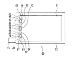
次に、図3を参照して、本発明に係る面状光源装置の第2の実施形態を説明する。図3は、本発明の第2の実施形態である面状照明装置40の要部を示す平面図である。この面状照明装置40は、上述した第1の実施形態と同様の構成要素を有してなるものであるが、各点状光源12〜14が配置される区画51〜53が、導光板41の入光面41cからハウジングフレーム42の側壁42aに向けて延在する突出部43〜46によって形成されている点で相違するものである。また、点状光源12〜14の側方に延在する粘着層47〜50は、その前側部分が導光板41の各突出部43〜46に、その後側部分がハウジングフレーム42の側壁42aに対応し、FPC15は、この粘着層47〜50によって、導光板41の入光面41cとハウジングフレーム42の側壁42aとを連結して一体化するように、導光板41およびハウジングフレーム42の両方に固着されている。
Next, a second embodiment of the planar light source device according to the present invention will be described with reference to FIG. FIG. 3 is a plan view showing a main part of the
ここで、本実施形態における面状装置40では、粘着層47〜50の前端47a〜50aが点状光源12〜14の光出射面(導光板41の入光面41cに対向する面)とほぼ同面に配置され、図1(a)および図2(b)に示すような光出射面から突出する部分(l)を有さないため、図3に示す点状光源13によって例示するような水平方向に広角に出射される光(A)を、使用する点状光源の指向特性によらずに確実に回避することができる。この際、粘着層47〜50の前端47a〜50aは、FPC15と導光板41との十分な密着面積を確保するため、上述したように点状光源12〜14の光出射面とほぼ同面に配置することが好ましいが、粘着層47〜50の前端47a〜50aを点状光源12〜14の光出射面よりも後方に配置するものであってもよい。
Here, in the
また、本実施形態における面状照明装置は、図4に示す面状照明装置60のように、導光板61側の突設部63〜66にそれぞれ対向する突設部67〜70をハウジングフレーム62側に形成し、それらの両方の突設部63〜66、67〜70によって形成される区画75〜77に点状光源12〜14を配置するものであってもよい。この場合でも、各粘着層47〜50は、図3に示す粘着層47〜50と同様のものとすることができる。さらに、図3および図4に示す面状照明装置40、60において、各区画51〜53、75〜77の形状、および各区画のハウジングフレーム42、62側のコーナー部の形状、粘着層47〜50のハウジングフレーム42、62側の形状等は、図2に基づいて上述した第1の実施形態の場合と同様に形成することができる。
In addition, the planar illumination device according to the present embodiment includes the projecting
なお、上述したすべての実施形態を通じて、点状光源は、略四辺形の導光板の一端面に配置されるものとしたが、本発明は、任意の形状の導光板の複数の端面に対して点状光源を配置する場合を含むものである。また、本発明において、点状光源が実装されたフレキシブルプリント基板は、導光板の対向する二つの主面のうちいずれの主面に固着されるものであってもよい。 In addition, although the point light source shall be arrange | positioned at the one end surface of a substantially quadrilateral light-guide plate through all the above-mentioned embodiment, this invention is with respect to the several end surface of the light-guide plate of arbitrary shapes. This includes the case where a point light source is arranged. In the present invention, the flexible printed circuit board on which the point light source is mounted may be fixed to any main surface of the two main surfaces facing the light guide plate.
10,20,40,60 面状照明装置
11,41,61 導光板
12〜14 点状光源
15 フレキシブルプリント基板
16〜19,30,47〜50 粘着層
22〜25,67〜70 突出部(ハウジングフレーム側)
43〜46,63〜66 突出部(導光板側)
10, 20, 40, 60
43 to 46, 63 to 66 Projection (light guide plate side)
Claims (3)
前記フレキシブルプリント基板は、粘着層を介して前記導光板と前記ハウジングフレームとにまたがって一面上に固着され、
前記粘着層は、前記点状光源の前方を除いた領域に設けられていることを特徴とする面状照明装置。 A light guide plate having one or more end faces as a light incident surface, a point light source disposed so as to face the light incident surface of the light guide plate, a flexible printed circuit board on which the point light source is mounted, and the light guide plate In a planar lighting device comprising a frame-shaped housing frame that holds
The flexible printed circuit board is fixed on one surface across the light guide plate and the housing frame via an adhesive layer,
The planar lighting device, wherein the adhesive layer is provided in a region excluding the front of the point light source.
Priority Applications (1)
| Application Number | Priority Date | Filing Date | Title |
|---|---|---|---|
| JP2004065707A JP3985231B2 (en) | 2004-03-09 | 2004-03-09 | Surface lighting device |
Applications Claiming Priority (1)
| Application Number | Priority Date | Filing Date | Title |
|---|---|---|---|
| JP2004065707A JP3985231B2 (en) | 2004-03-09 | 2004-03-09 | Surface lighting device |
Publications (2)
| Publication Number | Publication Date |
|---|---|
| JP2005259374A JP2005259374A (en) | 2005-09-22 |
| JP3985231B2 true JP3985231B2 (en) | 2007-10-03 |
Family
ID=35084911
Family Applications (1)
| Application Number | Title | Priority Date | Filing Date |
|---|---|---|---|
| JP2004065707A Expired - Lifetime JP3985231B2 (en) | 2004-03-09 | 2004-03-09 | Surface lighting device |
Country Status (1)
| Country | Link |
|---|---|
| JP (1) | JP3985231B2 (en) |
Cited By (1)
| Publication number | Priority date | Publication date | Assignee | Title |
|---|---|---|---|---|
| CN111123577A (en) * | 2018-11-01 | 2020-05-08 | 京东方科技集团股份有限公司 | Backlight module, manufacturing method thereof and liquid crystal display device |
Families Citing this family (12)
| Publication number | Priority date | Publication date | Assignee | Title |
|---|---|---|---|---|
| JP4579816B2 (en) * | 2005-12-09 | 2010-11-10 | 株式会社リコー | Illumination device, image reading device, and image forming device |
| JP5387210B2 (en) * | 2009-07-30 | 2014-01-15 | カシオ計算機株式会社 | Backlight device and liquid crystal display device |
| US8118465B2 (en) | 2009-10-30 | 2012-02-21 | Minebea Co., Ltd. | Spread illuminating apparatus |
| KR101604096B1 (en) * | 2010-01-04 | 2016-03-16 | 엘지이노텍 주식회사 | Backlight apparatus |
| JP6032949B2 (en) * | 2012-05-31 | 2016-11-30 | キヤノン株式会社 | Image reading device |
| JP6166612B2 (en) | 2013-07-31 | 2017-07-19 | ミネベアミツミ株式会社 | Surface lighting device |
| JP6303646B2 (en) * | 2014-03-13 | 2018-04-04 | オムロン株式会社 | Surface light source device |
| JP6246748B2 (en) | 2015-01-28 | 2017-12-13 | ミネベアミツミ株式会社 | Surface lighting device |
| US10107955B2 (en) * | 2015-04-27 | 2018-10-23 | Boe Technology Group Co., Ltd. | Display backlight module having double-side adhesive blocks |
| CN104748020B (en) * | 2015-04-27 | 2017-08-29 | 京东方科技集团股份有限公司 | Backlight module and display panel, display device |
| JP6684751B2 (en) * | 2017-06-02 | 2020-04-22 | ミネベアミツミ株式会社 | Area lighting device |
| CN115267963B (en) * | 2022-08-25 | 2024-04-05 | 北京京东方显示技术有限公司 | Backlight module and display device |
-
2004
- 2004-03-09 JP JP2004065707A patent/JP3985231B2/en not_active Expired - Lifetime
Cited By (2)
| Publication number | Priority date | Publication date | Assignee | Title |
|---|---|---|---|---|
| CN111123577A (en) * | 2018-11-01 | 2020-05-08 | 京东方科技集团股份有限公司 | Backlight module, manufacturing method thereof and liquid crystal display device |
| CN111123577B (en) * | 2018-11-01 | 2021-08-24 | 京东方科技集团股份有限公司 | Backlight module, manufacturing method thereof and liquid crystal display device |
Also Published As
| Publication number | Publication date |
|---|---|
| JP2005259374A (en) | 2005-09-22 |
Similar Documents
| Publication | Publication Date | Title |
|---|---|---|
| CN107247364B (en) | Backlight module and display device | |
| CN107544111B (en) | Planar lighting device | |
| US7677783B2 (en) | Backlight module with point light source having light guide portion | |
| JP2008090306A (en) | Liquid crystal display device | |
| JP2011060561A (en) | Surface light source device and liquid crystal display device | |
| JP2003215546A (en) | Liquid crystal display | |
| JP3985231B2 (en) | Surface lighting device | |
| JP5373180B2 (en) | Surface light source device and liquid crystal display device including the surface light source device | |
| KR20070120480A (en) | Liquid crystal display device | |
| JP2005243533A (en) | Planar lighting system | |
| JP2007087782A (en) | Planar light source device | |
| JP2007141596A (en) | Illumination device, electro-optical device, and electronic apparatus | |
| JP5447944B2 (en) | Surface lighting device | |
| JP2005267881A (en) | Planar lighting device | |
| JP2007059168A (en) | Backlight | |
| JP4623613B2 (en) | Image display device and surface light source device | |
| JP2010113982A (en) | Liquid crystal display device | |
| JP2008027649A (en) | Light source apparatus and backlighting apparatus | |
| JP4226511B2 (en) | Illumination device and liquid crystal display device | |
| JP2005235560A (en) | Planar lighting device | |
| JP4139644B2 (en) | Light guiding device, electro-optical device, and electronic apparatus | |
| JP2004349019A (en) | Surface light source device | |
| JP2005227720A (en) | Liquid crystal display device | |
| JP2009238406A (en) | Back light unit and reflective sheet | |
| JP7299422B2 (en) | Planar lighting device |
Legal Events
| Date | Code | Title | Description |
|---|---|---|---|
| A131 | Notification of reasons for refusal |
Free format text: JAPANESE INTERMEDIATE CODE: A131 Effective date: 20070214 |
|
| A521 | Written amendment |
Free format text: JAPANESE INTERMEDIATE CODE: A523 Effective date: 20070406 |
|
| TRDD | Decision of grant or rejection written | ||
| A01 | Written decision to grant a patent or to grant a registration (utility model) |
Free format text: JAPANESE INTERMEDIATE CODE: A01 Effective date: 20070620 |
|
| A61 | First payment of annual fees (during grant procedure) |
Free format text: JAPANESE INTERMEDIATE CODE: A61 Effective date: 20070628 |
|
| R150 | Certificate of patent or registration of utility model |
Ref document number: 3985231 Country of ref document: JP Free format text: JAPANESE INTERMEDIATE CODE: R150 Free format text: JAPANESE INTERMEDIATE CODE: R150 |
|
| FPAY | Renewal fee payment (event date is renewal date of database) |
Free format text: PAYMENT UNTIL: 20100720 Year of fee payment: 3 |
|
| FPAY | Renewal fee payment (event date is renewal date of database) |
Free format text: PAYMENT UNTIL: 20110720 Year of fee payment: 4 |
|
| R250 | Receipt of annual fees |
Free format text: JAPANESE INTERMEDIATE CODE: R250 |
|
| FPAY | Renewal fee payment (event date is renewal date of database) |
Free format text: PAYMENT UNTIL: 20110720 Year of fee payment: 4 |
|
| FPAY | Renewal fee payment (event date is renewal date of database) |
Free format text: PAYMENT UNTIL: 20120720 Year of fee payment: 5 |
|
| R250 | Receipt of annual fees |
Free format text: JAPANESE INTERMEDIATE CODE: R250 |
|
| FPAY | Renewal fee payment (event date is renewal date of database) |
Free format text: PAYMENT UNTIL: 20120720 Year of fee payment: 5 |
|
| FPAY | Renewal fee payment (event date is renewal date of database) |
Free format text: PAYMENT UNTIL: 20130720 Year of fee payment: 6 |
|
| R250 | Receipt of annual fees |
Free format text: JAPANESE INTERMEDIATE CODE: R250 |
|
| R250 | Receipt of annual fees |
Free format text: JAPANESE INTERMEDIATE CODE: R250 |
|
| R250 | Receipt of annual fees |
Free format text: JAPANESE INTERMEDIATE CODE: R250 |
|
| R250 | Receipt of annual fees |
Free format text: JAPANESE INTERMEDIATE CODE: R250 |
|
| R250 | Receipt of annual fees |
Free format text: JAPANESE INTERMEDIATE CODE: R250 |
|
| R250 | Receipt of annual fees |
Free format text: JAPANESE INTERMEDIATE CODE: R250 |
|
| R250 | Receipt of annual fees |
Free format text: JAPANESE INTERMEDIATE CODE: R250 |
|
| R250 | Receipt of annual fees |
Free format text: JAPANESE INTERMEDIATE CODE: R250 |
|
| S533 | Written request for registration of change of name |
Free format text: JAPANESE INTERMEDIATE CODE: R313533 |
|
| R350 | Written notification of registration of transfer |
Free format text: JAPANESE INTERMEDIATE CODE: R350 |
|
| R250 | Receipt of annual fees |
Free format text: JAPANESE INTERMEDIATE CODE: R250 |