JP3979599B2 - Nuclear medicine imaging device - Google Patents
Nuclear medicine imaging device Download PDFInfo
- Publication number
- JP3979599B2 JP3979599B2 JP2003183274A JP2003183274A JP3979599B2 JP 3979599 B2 JP3979599 B2 JP 3979599B2 JP 2003183274 A JP2003183274 A JP 2003183274A JP 2003183274 A JP2003183274 A JP 2003183274A JP 3979599 B2 JP3979599 B2 JP 3979599B2
- Authority
- JP
- Japan
- Prior art keywords
- time
- rise time
- rays
- ray
- detection
- Prior art date
- Legal status (The legal status is an assumption and is not a legal conclusion. Google has not performed a legal analysis and makes no representation as to the accuracy of the status listed.)
- Expired - Fee Related
Links
Images


Landscapes
- Measurement Of Radiation (AREA)
- Nuclear Medicine (AREA)
Description
【0001】
【発明の属する技術分野】
本発明は、放射性同位元素(RI)によって標識された薬剤を患者等の被検体に投与し、そのRIから放出されるγ線を検出して、被検体内のRI分布を取得する核医学撮像装置に関する。
【0002】
【従来の技術】
患者等の被検体にRIによって標識された放射性薬剤(以下、単に、薬剤という)を投入し、そのRIから放出されるγ線を検出して、被検体内のRI分布を取得する装置を総じて核医学撮像装置と呼ぶ(例えば特許文献1参照)。核医学撮像装置の代表的なものとしては、ガンマカメラやシングルフォトンエミッションCT(SPECT)、ポジトロンエミッションCT(PET)等がある。
【0003】
ガンマカメラは、被検体内から放出されるγ線を平面型検出器によって測定し、その平面分布をイメージングする装置であり、平面型検出器の前面にはコリメータを取り付け、γ線の入射方向を制限して指向性を与えている。平面型検出器は複数の放射線検出器を複数列及び複数行に配置している。
【0004】
単光子放出型断層写真撮影装置(SPECT装置)は、前記のガンマカメラと同様の平面型検出器を被検体の周囲に配置して被検体内から放出されるγ線を検出し、X線CTと同様に画像化処理して被検体の断層像を得る装置である。SPECT装置についてもガンマカメラと同様に、平面型検出器の前面にコリメータを取り付け、γ線の入射方向を制限している。SPECT装置に用いられるRIは単一のγ線を放出する核種(例えば99mTcや123I等)が用いられる。SPECT装置は少なくともいずれかのRIの被検体内での分布を画像化し、臓器の循環、代謝情報を知ることができる。
【0005】
陽子放出型断層写真撮影装置(PET装置)は、被検体周囲に配置したリング状検出器によって被検体内から放出されるγ線を検出し、このγ線の検出信号を基に画像化処理して被検体内のRI分布を示す断層像を得る装置である。リング状検出器は環状に且つベッドの長手方向に配置された多数の放射線検出器を有する。そのPET装置は、陽電子(β+)を放出する核種によって標識した薬剤を被検体に投与し、β+を放出して電子と結合し消滅する際に、ほぼ反対方向(180±0.6°)に放出する511keVの一対のγ線を検出対象としている。
【0006】
PET装置は、同じタイミングで検出された一対のγ線を同時計数装置で選出すれば、一対のγ線の入射方向を判別することができる。このため、PET装置は、ガンマカメラやSPECT装置と異なりコリメータを使用する必要がない。PET装置に用いられる陽電子放出核種には18F、15O、11C等がある。例えば18Fで標識した薬剤であるフルオロデオキシグルコース(2-[F-18]fluoro-2-deoxy-D-glucose,18F-FDG)は、被検体内に投与されたとき、糖代謝により腫瘍組織に高集積することを利用し、腫瘍部位の特定に使用される。
【0007】
ところで、従来の核医学撮像装置においては、γ線を検出する放射線検出器として、主に酸化ビスマスゲルマニウム(BGO)やタリウム添加ヨウ化ナトリウム(NaI(Tl))等の物質で構成されたシンチレータを用いている。この放射線検出器は、入射したγ線をシンチレータによって一旦微弱な光に変換し、この微弱な光を光電子増倍管やフォトダイオード等で電気信号に変換する。そのため、核医学撮像装置が大型化してしまうという問題があった。
【0008】
そこで、現在テルル化カドミウム(CdTe)やテルル化カドミウム亜鉛(CdZnTe)等の半導体セルで構成される半導体放射線検出器(以下、半導体検出器という)が注目されている(例えば特許文献2参照)。これら半導体検出器はγ線を電荷キャリア(電子と正孔)へと直接的に変換する。従って、個々の半導体セルでγ線を検出できるため、シンチレータと光電子増倍管を用いた場合に比べ装置の小型軽量化が期待できる。また、生成される電荷キャリア数も、シンチレータ検出器によって得られる数に比べて非常に多く、この事は良好なエネルギー分解能を得られることを意味している。
【0009】
【特許文献1】
特開平11−337645号公報(段落番号[0002]、図1)
【特許文献2】
特開2003−79614号公報(段落番号[0016]、図1)
【0010】
【発明が解決しようとする課題】
本発明の目的は、半導体放射線検出器を用いた場合にノイズのより少ない画像を得ることができる核医学撮像装置を提供することにある。
【0011】
【課題を解決するための手段】
前記目的を達成するため、本発明では、誘起電荷量に対応して半導体放射線検出器から出力される電圧信号(γ線検出信号)の立ち上がり時間を解析する機能と、立ち上がり時間に基づいて、半導体検出器の半導体検出部内の吸収時刻を精度良く求めるための時刻補正情報を与える機能とを備えたことを特徴とする。
【0012】
好ましくは、半導体検出部によるγ線の吸収によって放射線検出器から出力されるγ線検出信号の受信タイミングに対応して得られた第1吸収時刻情報を、γ線検出信号の立ち上がり時間を用いて得られた時刻補正情報により補正して第2吸収時刻情報を生成し、第2吸収時刻情報により選択された複数対のγ線検出信号を基に得られた情報により画像を生成することにある。この複数対のγ線検出信号を基に得られた情報には、具体的な例である補正用演算装置から出力されて選択された2つのデジタル信号を1つの信号として計数して得られる計数値が含まれる。
【0013】
好ましくは、予め電圧信号の立ち上がり時間と半導体検出素子内の吸収時刻との相関を求めるための立ち上がり時間−時刻補正値特性データ(時刻補正データ生成装置で使用)、及び電圧信号の立ち上がり時間と半導体検出素子内の吸収位置との相関を求めるための立ち上がり時間−吸収位置特性データ(位置補正データ生成装置で使用)を作成する。立ち上がり時間解析器と、立ち上がり時間−時刻補正値特性データを内蔵した時刻補正データ生成装置及び立ち上がり時間−吸収位置特性データを内蔵した位置補正データ生成装置を含む補正データ生成装置を撮像装置の装置系に組み込む。この補正データ生成装置は時刻補正データ生成装置と位置特定装置を統合した装置である。時刻補正データ生成装置に基づいた補正値を時刻補正装置に入力し、検出時刻から補正値を差し引いた値を吸収時刻として出力する。さらに位置補正データ生成装置に基づいた吸収位置データから検出器アドレス(検出器内の吸収位置)を新たなアドレスデータとして出力する。
【0014】
前述の立ち上り時間−時刻補正値特性データ及び立ち上がり時間−吸収位置特性データは撮像装置の稼働前に生成し、その後、半導体放射線検出器の経時特性に応じて定期的に特性試験を実施し、それらの特性データを更新することができる。また、それらの特性データにおける立ち上がり時間の区画及び吸収位置の区画の数は、要望された分解能、画質に応じて調整することができる。
【0015】
補正データ生成装置は1つの半導体放射線検出器に1個設けても良いが、入射γ線のに応じて複数の半導体放射線検出器毎に一つ設けて処理することもできる。なお、個々の半導体検出素子(半導体検出部)の特性を考慮し、補正データ生成装置内の特性データを個々の補正データ生成装置毎に設定してもよいが、吸収位置の区画数が数個程度であれば個々の補正データ生成装置毎に特性データを設定する必要はなく、代表的な一特性データを複数もしくは全ての補正データ生成装置に適用してもよい。このような場合でも、十分に時刻補正や吸収位置の精度の向上を図ることができる。
【0016】
【発明の実施の形態】
発明者等は、半導体検出器を適用した核医学撮像装置を詳細に検討した際に新たな課題を発見した。発明者等が発見した、半導体検出器における新たな課題を以下に詳細に説明する。半導体検出器にγ線が入射した時に内部で発生する現象を図10及び図11を用いて詳細に説明する。
【0017】
図10に示すように、半導体検出器60は、例えばCdTeで構成される半導体検出素子69と、この半導体検出素子69の両端に形成されたアノード63及びカソード64とによって構成されている。入射γ線65はこの半導体検出器60に入射し、半導体検出素子69内部の異なるγ線吸収位置66A,66Bで半導体検出素子69と相互作用を起こす。半導体検出素子69の内部では入射γ線65の吸収により電子67と正孔68を生成する。半導体検出素子69には電圧が印加されているため、電子67はアノード63に、正孔68はカソード64に向かってそれぞれ移動する。
【0018】
これら電荷キャリア(電子67、正孔68)の移動により半導体検出素子69の両端で電荷が誘起され、後段の増幅器(図示せず)によって誘起電荷量に比例した電圧信号が出力される。後段の信号処理装置(図示せず)では、この電圧信号から検出することにより入射γ線65の検出時刻及びエネルギーを認識する。
【0019】
図11(a)、(b)に、γ線吸収位置66A、66Bにおける出力電圧信号の時間経過を示す。ここで、この増幅器から出力される電圧信号の時間経過は2つの成分から構成され、1つは電子による高速成分であり、もう1つは正孔による低速成分である。これらの違いは移動度の違いに起因しており、例えばCdTeにおいては電子67の移動度が約1100cm2/V/秒、正孔68の移動度が約100cm2/V/秒と、およそ1桁異なる。
【0020】
即ち、これは、電圧信号の時間経過が半導体検出素子69内のγ線吸収位置66A,66Bに依存して変化することを意味する。カソード64の近傍であるγ線吸収位置66Aでγ線が吸収されると、低速な正孔成分32Aでもカソード64までの距離が短いために短時間で電荷が誘起される。電子成分31Aについてもアノード63までの距離は長いが高速なために短時間で電荷が誘起される。この結果、正孔成分31Aと電子成分31Bの両成分を足し合わせた電圧信号33Aも高速で立ち上がり(図11(a)中のΔT参照)、最大値に達した後、徐々に減衰していく。
【0021】
一方、アノード63の近傍であるγ線吸収位置66Bでγ線が吸収されると、電子成分31Bはアノード63までの距離が短いために非常に短時間で電荷が誘起されるが、逆に正孔成分32Bはカソード64までの距離が長く、低速なため、立ち上がりが遅い(図11(b)中のΔT参照)。従って電圧信号33Bが最大値に達する時間も長くなる。また、正孔68はカソード64への移動時にトラップされてしまい十分に収集することができなくなるため、吸収位置30Aで得られる程の誘起電荷量に及ばず、信号量欠損の原因となる。このように、半導体検出器においてγ線吸収位置によっては信号欠損が生じると、この半導体検出器の出力であるγ線検出信号に基づいて得られる情報を用いて作成される患者の画像情報に対してノイズになるという新たな課題を、発明者等が見出した。
【0022】
前述のように、γ線吸収位置66A、66Bの違いによる出力信号の変化は、主として低速成分である正孔に依存している。例えばCdTeでは、Si(電子:1500cm2/V/秒、正孔:500cm2/V/秒)やGe(電子:3900cm2/V/秒、正孔:1900cm2/V/秒)に比べて電子、正孔共に移動度が遅く、しかも電子と正孔とで移動度の違いが大きいことから、電圧信号33Bの最大値に達する時間が長くなる傾向が顕著となる。
【0023】
発明者等は、半導体検出器において生じる上記の現象が核医学撮像装置にとって次のような損失をもたらすことを新たに見出した。すなわち、例えばPET装置において同時に放出される一対のγ線を検出し、この一対のγ線が同時に入射されたと判別する場合、予め同時計数時間窓と呼ばれる時間幅を設定しておき、この時間幅内に得られた2つの検出事象を同時と判定する。この時間幅は小さい程好ましい。なぜならその時間幅が大きいと、その時間幅内で一対のγ線を検出する(真の同時計数)だけでなく、体内の他の箇所でも発生したγ線を検出する(偶発同時計数)機会が増えるためである。偶発同時計数は偽の現象であり、被検体の画像(断層像)に対するノイズの原因となる。
【0024】
一方、シンチレータ検出器の場合、発光現象を利用しているため入射γ線は検出素子内部のどこで吸収されても信号の立ち上がりはほとんど変わらないので、入射γ線が吸収された瞬間の時刻(γ線吸収時刻)と後段のタイミング検出装置で信号を検出する時刻(検出時刻)との時間差が吸収された位置に対してほとんど変化せず、また信号の立ち上がりが速い。従ってシンチレータ検出器においては同時検出する性能に優れ、いわゆる同時計数分解能を示す半値幅は短く、約10[ns]であり、時間幅もほぼ同程度に設定できる。
【0025】
ところが、CdTe等の半導体検出器では前述の様に吸収位置に依存して信号の立ち上がりが変化するため、γ線吸収時刻と検出時刻のばらつきが大きくなる。このため半値幅は20[ns]程度と大きくする必要があり、同時計数時間窓と呼ばれる時間幅も同様に大きく設定しなければならない。そこで、半導体検出器を用いた場合において被検体の画像(断層像)の画質を向上させるためにも、半導体検出器を用いた場合においてもシンチレータ検出器に劣らない程度の同時計数分解能を保証する必要がある。
【0026】
発明者等は、上記した新たに発見した課題を解消するために、すなわち画像におけるノイズの低減を図るために本発明をなしたのである。その新たな課題を解消するために種々検討して得られた本発明の具体的な実施の形態を、以下に説明する。
【0027】
(第1の実施の形態)
次に、本発明の第1の実施の形態である核医学撮像装置、具体的にはPET装置を、図1ないし図6を参照して詳細に説明する。なお、本実施の形態では、同一の要素については番号の次にアルファベット小文字で付し、重複した説明を省略する。
【0028】
まず、本実施の形態のPET装置の時刻補正データ生成装置17及び位置補正データ生成装置18(図5)に用いる立ち上り時間ΔTと検出時刻差Δτとの関係を示す特性、及び立ち上り時間ΔTと吸収位置Δx(N’)との関係を示す特性を得る試験装置Aを、図1を用いて説明する。試験装置Aは、半導体検出器1a、1bと、負の高圧電源5と、半導体検出器1a、1bで誘起された電荷を増幅する前置増幅器6a、6bと、前置増幅器6a、6bの出力を高速で波形整形して増幅する高速増幅器7a、7bと、この高速増幅器7a、7bの出力信号のタイミングを検出するタイムピックオフ装置8a、8bと、タイムピックオフ装置8aからの出力信号を所定時間遅らせる遅延装置9と、2つのタイムピックオフ装置8a、8bから出力されたタイミングパルスの時間差に比例した波高のパルスを出力する時間波高変換器10と、高速増幅器7aの出力波形の立ち上がり時間に比例した波高のパルスを出力する立ち上がり時間解析器11とから構成される。なお、半導体検出器1a、1bは、約5mm角の2つの半導体検出素子2a、2bと、電圧印加電極(陽極)であるアノード3a、3bと、陰極であるカソード4a、4bとを備えている。
【0029】
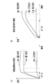
2つの半導体検出器1a、1bの間に22Na等の陽電子放出核種の標準線源12及び穴径が約100μmの鉛製コリメータ13を設置する。まず初めは、半導体検出器1a、1bのカソード4a、4bをコリメータ13の出口側に配置する。従って、標準線源12が放出した陽電子の消滅により発生する一対のγ線29、29は、半導体検出器1a、1bのカソード4a、4b近傍に入射する。半導体検出素子2a、2b内部にγ線が吸収されたことにより誘起された各電荷は、図4に示すように、波形36Aの形で発生する。その電荷を入力した前置増幅器6a、6bは波形37Aの電圧信号を出力する。この電圧信号を入力した高速増幅器7a、7bは波形37Aの立ち上がり波形を有した波形38Aの電圧信号を出力する。高速増幅器7aの出力信号はタイムピックオフ装置8a及び立ち上がり時間解析器11に入力される。高速増幅器7bの出力信号はタイムピックオフ装置8bに入力される。タイムピックオフ装置8a、8bは、例えばコンスタントフラクション方式等でタイミングパルスを出力する。時間波高変換器10は両タイミングパルスの検出時刻差(時刻補正値)Δτに比例した波高のパルスを出力する。
【0030】
一方、立ち上がり時間解析器11は、例えば入力信号波高の10%から90%までに経過した立ち上がり時間ΔTに比例した波高のパルスを出力する。現在の状態(図1の状態)では、一対のγ線29、29がそれぞれカソード4a、4b付近で吸収されるため、前述したように、半導体検出素子2a、2b内部で発生する正孔成分と電子成分による電圧信号もそれぞれ高速で立ち上がり(図11(a)中のΔT参照)、両者のタイミング検出の時間差も小さい。即ち検出時刻差Δτも立ち上がり時間ΔTも小さい。
【0031】
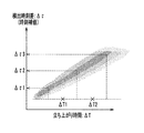
ここで、一方の半導体検出器1aを図1中の矢示a方向に移動して測定すると、半導体検出素子2a内の吸収位置はカソード4aから離れるために、半導体検出器1aで発生する電圧信号の立ち上がりが低速となる。このため、図4に示すように、半導体検出器1aから出力される誘起電荷の波形は36B、前置増幅器6aの出力である電圧信号の波形は37B、及び高速増幅器7aの出力である電圧信号の波形は38Bのようになる。これに伴って、検出時刻差Δτと立ち上がり時間ΔTが増加する。このように半導体検出器1aをコリメータ13に対して矢印a(図1)の方向に移動させることにより、図2に示すような立ち上がり時間ΔTと検出時刻差Δτとの相関、及び立ち上がり時間ΔTと半導体検出器1aの移動量Δx(以下、吸収位置Δxという)との相関を得ることができる。
【0032】
従って、図2に示す特性を基に入力された立ち上がり時間ΔTを検出時刻差(時刻補正値)Δτに変換し、得られた検出時刻差Δτを出力する時刻補正データ生成装置、及び図3に示す特性を基に入力された立ち上がり時間ΔTを吸収位置Δxに変換し、吸収位置Δx(以降の実施の形態では位置情報として吸収位置N′と表記する)を出力する位置補正データ生成装置をそれぞれ作成することができる。なお、図2、図3を見ても分かるようにΔT−Δτ特性、ΔT−Δx(N′)特性はばらつきをもった分布を有しており、1対1で変換することは困難である。そこで、例えば立ち上がり時間ΔTを、ΔT1、ΔT2を境として3つの時間区画に分け、時刻補正データ生成装置ではそれらの時間区画に対応してΔτ1、Δτ2、Δτ3に、及び位置補正データ生成装置ではそれらの時間区画に対応してΔN1′、ΔN2′、ΔN3′に変換してもよい。または、その3つの区画毎に立ち上がり時間ΔTと検出時刻差Δτとの第1関係式、及び立ち上がり時間ΔTと吸収位置N′との第2関係式をそれぞれ設定し、時刻補正データ生成装置は第1関係式を用いて立ち上がり時間ΔTに対応した検出時刻差Δτを、位置補正データ生成装置は第2関係式を用いて立ち上がり時間ΔTに対応した吸収位置N′を算出するようにしてもよい。
【0033】
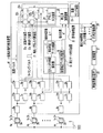
次に、図2に示すΔT−Δτ特性、図3に示すΔT−Δx(N′)特性を用いた本実施の形態に係るPET装置(核医学撮像装置の一種)を、図5を参照して説明する。まず、被検体(被検診者)Hに18F等の陽電子放出核種を標識した薬剤を投与し、薬剤が被検体H内を拡散して撮像可能な状態となるまで待機する。これにより、薬剤は被検体内の癌の患部に集積する。PET装置Pは、図5に示すように、例えばCdTeからなる半導体検出器1a、1b・・・1nをリング状に配置した構成となっている。撮像可能な状態になった被検体Hが横たわっているベッドBがPET装置P内に挿入される。この状態で、多数の半導体検出器が被検体Hの周囲を取り囲んでいる。それらの半導体検出器は、薬剤に起因して被検体Hから反対方向(180±0.6°)に放出される一対のγ線をそれぞれ検出する。このようにして、PET撮像が行われる。PET装置Pは、更に、γ線検出信号処理装置41、同時係数装置26及び画像再構成装置(画像作成装置)28を有する。PET装置Pに設置される多数の半導体検出器は、PET装置Pの周方向において複数の群に分割されている。γ線検出信号処理装置41は、それらの群ごとに設けられる。
【0034】
以下、図6に基づいて、1つのγ線検出信号処理装置41について説明する。各半導体検出器のカソード4a、4b・・・4nには高圧電源5から電圧が印加されている。被検体Hから放出されたγ線が各半導体検出器1の半導体検出素子(半導体検出部)2a、2b・・・2nに入射すると、γ線が半導体検出素子2によって吸収された場合、その吸収されたγ線のエネルギーに対応した量の電荷がアノード3a、3b・・・3n及びカソード4a、4b・・・4nにそれぞれ誘起される。それぞれの誘起電荷は、アノード3a、3b・・・3nに個々に接続されている前置増幅器6a、6b・・・6nにγ線検出信号として出力され、該当する前置増幅器によって増幅される。
【0035】
前置増幅器6a、6b・・・6nに個々に接続されている低速増幅器(比例増幅器)14a、14b、・・・14nのそれぞれは、前置増幅器6a、6b・・・6nのうちの該当する前置増幅器からの出力を入力して前述の誘起電荷量に応じた十分な波高を有する、図4に示す電圧波形39A(または電圧波形39B)を出力する。この電圧波形の波高はγ線エネルギー値を反映している。低速増幅器14a、14b、・・・14nに個々に接続されている波高保持装置15a、15b・・・15nのそれぞれは、該当する低速増幅器からの電圧波形39A(または電圧波形39B)を入力し、その電圧波形の波高値を有したパルス信号を信号処理装置20の波高弁別装置23a、23b、・・・23nに出力する。
【0036】
一方、前置増幅器6a、6b・・・6nに個々に接続されている高速増幅器7a、7b、・・・7nのそれぞれは、前置増幅器6a、6b・・・6nのうちの該当する前置増幅器から出力された信号の立ち上がりを高速で増幅し、図4に示す波形38A(または波形38B)の電圧信号を出力する。
【0037】
高速増幅器7a、7b、・・・7nのうち該当する高速増幅器からの電圧信号を入力するタイムピックオフ装置(時刻検出装置)8a、8b、・・・8nは、それぞれ、信号処理装置20の時刻判別装置(時刻付与装置)22a、22b、・・・22nのうち接続されている時刻判別装置に、その電圧信号の受信タイミングに応じてタイミングパルスを出力する。タイムピックオフ装置及び時刻判別装置は時刻決定装置を構成している。高速増幅器7a、7b、・・・7nの電圧信号は補正データ生成装置16の立ち上がり時間解析器(立ち上り時間発生装置)11にも入力される。立ち上がり時間解析器11は、高速増幅器7a、7b、・・・7nからのそれぞれの電圧信号を基にそれぞれの電圧信号の立ち上がり時間ΔTを計測し、時刻補正データ生成装置17及び位置補正データ生成装置18に出力する。補正データ生成装置16は、立ち上がり時間解析器11、立ち上がり時間解析器11から出力される立ち上がり時間ΔTを基に検出時刻差Δτを求める時刻補正データ生成装置17、その立ち上がり時間ΔTを基に吸収位置N′を求める位置補正データ生成装置18を備える。
【0038】
時刻補正データ生成装置17は、図2を基にして得られた時刻データ特性(例えば、立ち上がり時間ΔTと検出時刻差Δτの関係式)を用いて高速増幅器7a、7b、・・・7nのそれぞれの電圧信号の各立ち上がり時間ΔTに対して時刻補正値である検出時刻差Δτをそれぞれ求め、信号処理装置20の補正用演算装置25に出力する。これらの検出時刻差Δτは半導体検出器1a、1b・・・1nからそれぞれ出力されるγ線検出信号に対するものである。位置補正データ生成装置18は、図3を基にして得られた位置データ特性(例えば、立ち上がり時間ΔTと吸収位置N′の関係式)を用いて上記の各立ち上がり時間ΔTに対して半導体検出器1a、1b・・・1nの吸収位置N′をそれぞれ求め、信号処理装置20の補正用演算装置25に出力する。
【0039】
信号処理装置20では以下の処理が行われる。波高弁別装置23a、23b、・・・23nのそれぞれは、閾値以上の波高値を有するパルス信号を弁別して時刻判別装置22a、22b、・・・22nのうち該当する時刻判別装置に出力する。時刻判別装置22a、22b、・・・22nのそれぞれには、高速クロック装置19からのタイミングパルスであるクロック信号が入力される。各時刻判別装置は、波高値を有するパルス信号を、該当するタイムピックオフ装置からタイミングパルスを入力したときのクロック信号に対応した時刻τの時刻情報を有するデジタル信号に変換し、このデジタル信号を該当するアドレス判別装置24に出力する。時刻判別装置22a、22b、・・・22n及びアドレス判別装置24は時刻・アドレス判断装置21に含まれる。
【0040】
アドレス判別装置24は、時刻判別装置22a、22b、・・・22nのそれぞれから時刻τの時刻情報が付与されたデジタル信号を入力したとき、そのデジタル信号を出力した時刻判別装置が実質的に接続されている半導体検出器のアドレス情報Nがそのデジタル信号に付与される。アドレス判別装置24は時刻情報τ及びアドレス情報Nが付与されたデジタル信号を補正用演算装置25に出力する。アドレス情報は、PET装置Pに設けられた各半導体検出器ごとに付与されている。補正用演算装置25において、時刻τが検出時刻差(時刻補正値)Δτにより補正された時刻補正情報(τ−Δτ)が生成され、更に、アドレス情報Nに半導体検出器1内部の吸収位置N′の情報が付加された補正アドレス情報(N*N′)が生成される。補正用演算装置25は、時刻補正情報(τ−Δτ)及び補正アドレス情報(N*N′)が付与されているデジタル信号を同時計数装置26に出力する。
【0041】
本実施の形態では、前置増幅器、高速増幅器、タイムピックオフ装置、低速増幅器、波高保持装置、時間判別装置及び波高弁別装置は、それぞれ、半導体検出器ごとに設けられている。このため、1つの半導体検出器の出力であるγ線検出信号は、途中で信号形態が変わる場合もあるが、実質的にそれらの装置に入力されることになる。
【0042】
本実施の形態は、時刻補正データ生成装置17、及び補正用演算装置25における時刻τを検出時刻差Δτで補正する構成を含む時刻補正装置と、位置補正データ生成装置18、及び補正用演算装置25におけるアドレス情報Nに半導体検出器1内部の吸収位置N′の情報を付加する構成を含む位置補正装置を備えているとも言える。補正アドレス情報(N*N′)は、該当する半導体検出器のアドレス情報N(半導体検出器の番地)及びその半導体検出器内においてガンマ線が吸収された位置N′を含んでいるため、ガンマ線の吸収された位置を精度良く示している。吸収位置N′の情報をアドレス情報Nに付加することは、アドレス情報Nの補正に相当する。
【0043】
なお、図6に示した半導体検出器1及びγ線検出信号処理装置41の構成はPET装置Pに設けられたそれらの一部である。PET装置Pに設けられた多数の半導体検出器が、半導体検出器1a、1b・・・1nを1つの単位として、複数のグループに分割されている。それらの半導体検出器は、図5に示すように、グループ毎に異なるγ線検出信号処理装置41にγ線検出信号を出力する。それらのγ線検出信号処理装置41から出力された、時刻補正情報及び補正アドレス情報が付与されている各デジタル信号が、同時計数装置26に入力される。
【0044】
同時計数装置26は、各信号処理装置20の補正用演算装置25から出力されたデジタル信号を用いて同時計数を行う。すなわち、それらのデジタル信号に付与された時刻補正情報(τ−Δτ)のうち、同時計数時間窓w[ns]の時間内に入っている2つのデジタル信号を選択すると共に、同時計数によりそれらの2つのデジタル信号を1つの信号として計数する。同時係数装置26は、選別された2つの信号の補正アドレス情報の組み合わせ(一対の補正アドレス情報)、及び同時計数された信号の計数値(γ線対の発生数)の各情報を、同時計数装置26のメモリ(図示せず)に記憶する。
【0045】
画像再構成装置28は上記メモリ内の複数対の補正アドレス情報及び計数値を記憶装置27に記憶させる。その一対の補正アドレス情報が、上記一対のγ線29のそれぞれの飛行方向データに相当する。画像再構成装置28は、複数対の補正アドレス情報及び計数値を用いて、公知のフィルタバックプロジェクション法により各ボクセルにおけるγ線発生密度を求める。画像再構成装置28は、これらのγ線対発生密度に基づいて、放射性核種の集積位置、即ち腫瘍位置での断層画像を作成する。この断層像の情報は記憶装置27に記憶される。また、その断層像の情報は表示装置(図示せず)に表示される。
【0046】
なお、選択された2つのデジタル信号を1つの信号として計数して得られた計数値は、選択された2つのデジタル信号に対応する一対のγ線検出信号を基に得られた情報である。
【0047】
このように、本実施の形態によれば、補正データ生成装置16で得られた時刻補正値(検出時刻差)Δτを得ることができるため、この時刻補正値Δτを用いて、実際にγ線が半導体検出素子2で吸収された瞬間に近い時刻を、時刻補正情報(τ-Δτ)として同時計数判定することができる。すなわち、時刻補正値Δτを用いるので同時計数時間窓w[ns]を短く設定でき、偶発同時計数が低減される。このため、従来のPET装置に比べてノイズの少ない断層像を得ることができる。
【0048】
本実施の形態では、例えば、立ち上がり時間ΔTをΔT1とΔT2を境界にして3分割しているので、同時計数分解能は、後段の装置系(補正データ生成装置16、信号処理装置20、同時計数装置26等)による影響を考慮しても、従来の20[ns]程度から半分程度に小さく抑えられ、シンチレータの約10[ns]に匹敵する性能を発揮することができる。このため、得られる断層像の精度が更に向上する。従って、同時計数時間窓wの幅もシンチレータと同程度に設定することができ、高精度な時間分解能を得ることができる。
【0049】
アドレス情報も個々の半導体検出器1のアドレスNに加え、その内部でのγ線の吸収位置N′を付加したことにより、γ線が吸収された位置をより高精度に判別することができる。つまり、半導体検出器1及びそれに付随する装置の数を変化させることなく、計測上は実効的に半導体検出器内で3つの領域のうちどの領域でガンマ線が吸収されたのかを判別できるということは、1つの半導体検出器の寸法を3分の1に小型化して半導体検出器の数を3倍に増加した場合と同等である。このような本実施の形態では、結果的に画像上の空間分解能が大幅に向上できる。さらに、1つの補正データ生成装置16が設けられている本実施の形態は、γ線検出信号処理装置41の構成を単純化できる。なお、補正データ生成装置16は、放射線検出器ごとに設置し、該当する高速増幅器に接続してもよい。
【0050】
以上、本実施の形態によれば、容易に作成可能な立ち上がり時間解析器を用いて被検体に吸収されるγ線吸収の電圧信号の立ち上がり時間を計測し、時刻補正値及び吸収位置情報を付加することにより同時計数分解能及び空間分解能を向上できる。その結果、画質上の大幅なノイズ低減、空間分解能向上が実現できる。
【0051】
(第2の実施の形態)
本発明の第2実施の形態を、図7に基づいて説明する。本実施の形態に係る核医学撮像装置であるPET装置P1は、PET装置Pのγ線検出信号処理装置41をγ線検出信号処理装置51に替えた構成を有する。なお、本実施の形態では、第1の実施の形態と同一の構成要素に同一の符号を付し、その説明を省略するものとする。γ線検出信号処理装置51は、補正データ生成装置16に替えて検出時刻補正装置35を有する。検出時刻補正装置35は、タイムピックオフ装置8、立ち上がり時間解析器11、時刻補正データ生成装置17、遅延装置52及びパルス出力タイミング調整装置(以下、タイミング調整装置という)53を有し、半導体検出器ごとに設けられる。各検出時刻補正装置35は、高速増幅器7a、7b、・・・7nのうち該当する高速増幅器にそれぞれ接続される。位置補正データ生成装置18は、複数の補正データ生成装置16Aの立ち上がり時間解析器11からの立ち上がり時間ΔTを入力して半導体検出素子2内の吸収位置N′を算出し、吸収位置N′を信号処理装置20の補正用演算装置25に出力する。
【0052】
高速増幅器7a、7b、・・・7nからそれぞれ出力された電圧信号は、該当する検出時刻補正装置35のタイムピックオフ装置8及び立ち上がり時間解析器11にそれぞれ入力される。タイムピックオフ装置8は、前述したように、タイミングパルスを出力する。このタイミングパルスは遅延装置52で設定時間τd(以下、遅延時間τdという)だけ遅延された後にタイミング調整装置53に入力される。遅延装置52及びタイミング調整装置53は時刻調整装置を構成している。設定時間τdは、全ての遅延装置52において同一の値に設定されている。一方、立ち上がり時間解析器11は、該当する高速増幅器から入力される電圧信号の立ち上がり時間ΔTを計測し、時刻補正データ生成装置17及び位置補正データ生成装置18に出力する。
【0053】
時刻補正データ生成装置17は、求めた検出時刻差Δτをタイミング調整装置53に出力する。タイミング調整装置53は、設定時間τdだけ遅延されているタイミングパルスを、更に(τs−Δτ)だけ遅延させて時刻判別装置22に出力させる。ここで、τsは想定されるΔτに対して確実にτs>Δτとなるような値であり、全てのタイミング調整装置53で共通の値に設定されている。また、前記から分かるように遅延時間τdは、立ち上がり解析器11での立ち上がり時間ΔTの計測からタイミング調整装置53で(τs−Δτ)を求めるまでの処理のための待ち時間であり、前記処理が行える程度の時間に設定すればよい。結果として、各補正データ生成装置16Aのタイミング調整装置53から時刻判別装置22a、22b、・・・22nのうちの該当する時刻判別装置に出力される時刻は(τ+τd+τs−Δτ)となる。この時刻は、結局、第1の実施の形態における時刻補正情報(τ−Δτ)を、全ての補正データ生成装置16Aに共通な値(τd+τs)だけ遅延させた時刻である。従って、時刻判別装置22a、22b、・・・22nは第1実施の形態と同様に実質的に時刻補正情報(τ−Δτ)を取得することになる。
【0054】
一方、位置補正データ生成装置18は、図3の特性図を基にして得られた位置データ特性から半導体検出素子2内の吸収位置N′を算出し、補正用演算装置25に出力する。これにより、第1の実施の形態と同様に、時刻補正情報(τ−Δτ)と補正アドレス情報(N*N′)が付与されているデジタル信号を同時計数装置21に出力する。
【0055】
本実施の形態は、γ線検出信号処理装置41の構成の単純化を除いて、第1実施の形態で生じる効果を得ることができる。更に、本実施の形態は、タイミング調整装置53で受信したタイミングパルスが時刻判定装置22に出力される時刻を、予め補正データ生成装置16内部で調整する構成としているため、信号処理装置20の内部で時刻補正を行う必要がなくなり、信号処理装置20内部での論理設計を簡素化することができる。
【0056】
(第3の実施の形態)
次に、本発明の第3の実施の形態について図8に基づいて説明する。図8は第3の実施の形態に係る核医学撮像装置の一種であるガンマカメラの構成を示すブロック図である。本実施の形態は、時刻補正値等の時刻情報は特に必要がないため、時刻補正データ生成装置を設置していない。しかし、位置補正データ生成装置を備えている。なお、本実施の形態では、前記第1の実施の形態と同一の構成要素に同一の符号を付し、その説明を省略するものとする。
【0057】
半導体検出器1よりも被検体H側に鉛製のコリメータ13が設置される。コリメータ13は、開口部である複数のγ線通路61を形成する。半導体検出器1の幅が5mm程度であり、1つの半導体検出器1に対して3つのγ線通路61が対向している。γ線29がいずれの開口部61から半導体検出器1に入射したかは、後段の位置特定装置62を構成する立ち上がり時間解析器11で立ち上がり時間ΔTを計測し、位置補正データ生成装置18を基に半導体検出素子2内の吸収位置N′を求めることにより識別できる。このため、位置補正データ生成装置18は、1つの半導体検出器1に対向する3つのγ線通路の配置に対応して3通りの吸収位置N′が等間隔で決定されるように立ち上がり時間ΔTの区画の間隔を予め設定しある(図3参照)。
【0058】
本実施の形態におけるガンマカメラの作用について説明する。
まず、被検体Hに単光子放出型核種(例えば99mTc等)を含む放射性薬剤を投与する。この放射性薬剤が被検体H内を拡散し、撮像可能な状態となるまで待機する。被検体Hが横たわっているベッドを移動させて被検体Hを、平面状に配置されたCdTe半導体検出器1を用いたガンマカメラに近接させる。半導体検出器1に高圧電源5を印加し、γ線29の検出を開始する。被検体Hから放出されたγ線29がγ線通路61を通って半導体検出素子2に入射する。γ線29が半導体検出素子2内で吸収されると、そのエネルギーに応じた量の電荷(γ線検出信号)が誘起される。この電荷は前置増幅器6で増幅される。前置増幅器6からの出力信号は、低速増幅器14及び高速増幅器7に入力される。低速増幅器14で増幅された出力信号は波高保持装置15に入力され、波高保持装置15の出力である波高パルスが信号処理装置20の波高弁別装置23に出力される。高速増幅器7で増幅された出力信号は位置特定装置26の立ち上がり時間解析器11に入力される。
【0059】
立ち上がり時間解析器11は、第1の実施の形態と同様に、立ち上がり時間ΔTを計測する。位置補正データ生成装置18は、計測された立ち上がり時間ΔTに対応する吸収位置情報N′を求め、この吸収位置情報N′を信号処理装置20の補正用演算装置25に出力する。
【0060】
波高弁別装置23は波高保持装置15から出力される波高パルスのうち閾値以上の波高値を有する波高パルスを弁別する。アドレス判別装置24は、各波高弁別装置23から出力された波高パルスをそれぞれ入力し、該当する半導体検出器1のアドレスNを判別する。アドレス判別装置24は入力した波高パルスをアドレスNの情報を付与したデジタル信号に変換し、このデジタル信号を出力する。そして補正用演算装置25は、吸収位置N′の情報を前記アドレスNに付加した補正アドレス情報(N*N′)を付与したデジタル信号を計数装置(図示せず)に出力する。計数装置は、複数の信号処理装置20、すなわち補正用演算装置25からのそれぞれのデジタル信号を計数して得られる各計数値及び該当する補正アドレス情報を、計数装置のメモリ(図示せず)に記憶する。画像再構成装置28は、上記メモリに記憶された補正アドレス情報及びその計数値、及び前述のフィルタバックプロジェクション法を用いて、被検体Hに対する平面画像を生成する。この画像は表示装置(図示せず)に表示される。
【0061】
以上、本実施の形態によれば、位置特定装置62で吸収位置N'を求めることによって、半導体検出器1の幅(患者の体軸方向における長さ)よりも小さなγ線通路61を有するコリメータ13を配置しても、1つの半導体検出器1にどのγ線通路61からγ線29が入射したかを識別でき、結果的に空間分解能を大幅に向上することができる。しかも、容易に作成可能な位置特定装置62を備えるだけで、半導体検出器1の数及びそれに付随する装置数を増やすことなくガンマカメラをコンパクト化することができる。
【0062】
このガンマカメラは、1つないし複数の平面状半導体検出器を、被検体の周囲で回転させることによりSPECT装置として使用することも可能である。
【0063】
(第4の実施の形態)
本発明の第4の実施の形態について図9に基づいて説明する。図9は、第4の実施の形態に係る医学撮像装置の一種であるガンマカメラの構成を示すブロック図である。本実施の形態でも第3の実施の形態と同様に時刻補正データ生成装置を設置していない。なお、本実施の形態では、前記第1の実施の形態と同一の構成要素に同一の符号を付し、その説明を省略するものとする。
【0064】
本実施の形態も半導体検出器1よりも被検体H側に鉛製のコリメータ13が設置される。約5mmの幅を有する1つの半導体検出器1に対してコリメータ13に形成される1つのγ線通路61が対向している。コリメータ13は半導体検出器1の相互間に挿入されており、γ線通路61の幅は半導体検出器1の幅に等しい。半導体検出器1のアノード3は、γ線通路61に対向している。カソード4はアノード3と平行になるように半導体検出素子2に設けられる。半導体検出器1及びコリメータ13の幾何学的形状から、半導体検出器1にはαで表される視野角からγ線が入射し得る。
【0065】
しかし、半導体検出素子2内部の吸収領域を3つの吸収領域71A、71B、71Cに分割し、被検体から最も遠い吸収領域71Cのみを選別した場合、これは実効的にコリメータ13の高さが増加したことを意味し、この吸収領域71Cに入射するγ線の視野角はβと小さい。
【0066】
前者の大視野角αで撮像する場合は、画像再構成装置27で得られる画像の空間分解能は粗いがγ線の計数率が高く短時間で検査が行える。これを通常検査モード(短時間簡易モード)と呼ぶ。一方、後者の小視野角βでは吸収領域71Cで吸収された事象のみを選択するため、計数率は低く検査時間はかかるが空間分解能が優れた画像が得られる。これを高分解能検査モードと呼ぶ。本実施の形態では、被検体Hである検査者の要望に応じ検査モードを変えることができる。例えば分解能は低くとも短時間検査を必要とする場合には通常検査モードで使用し、より高分解能な検査を要する場合には高分解能検査モードで使用すればよい。
【0067】
検査モード、すなわち通常検査モード及び高分解能検査モードの設定は、検査者が予め制御器72の入力画面等で選択できるものとする。制御器72は、動作設定信号により、通常検査モードではガンマ線が上記3つの吸収領域のどの領域で吸収されたかにかかわらずガンマ線が1つの半導体検出器に入射した場合に該当する半導体検出器のアドレスNの情報を付加したデジタル信号を出力するように、高分解能検査モードでは位置特定装置18からの許可信号を入力した場合のみにアドレスNの情報を付加したデジタル信号を出力するように、アドレス判別装置24を設定する。通常検査モードを選択した場合、半導体検出器1のアドレスNのみが識別できればよいので位置特定装置73を起動する必要はない。制御器72は、通常検査モードでは位置特定装置73へ停止命令を送信し、位置特定装置73からの許可信号の出力を阻止する。通常検査モードでは、第3実施の形態と同様に、計数装置(図示せず)が、アドレス判別装置24から出力された、アドレスNの情報を付加したデジタル信号を計数し、この計数値及びアドレスNを計数装置のメモリ(図示せず)に記憶する。画像再構成装置28は、そのメモリ入力したアドレスN及び計数値を用いて実施の形態3と同様に再構成処理を行い、放射性核種の集積位置の平面画像を生成する。この画像は表示装置(図示せず)に表示される。
【0068】
一方、制御器72は、高分解能検査モードを開始する際に起動命令を、高分能検査モードを終了する際に停止命令を、位置特定装置73にそれぞれ送信する。位置特定装置73は、起動命令を入力して停止命令を入力する間、吸収領域71Cでガンマ線が吸収されたときにアドレス判別装置24に許可信号を出力する。すなわち、位置特定装置73は、立ち上がり時間解析器11で算出した立ち上がり時間ΔTが吸収領域71Cに該当する値である場合にアドレス判別装置24に許可信号を送信する。起動命令を入力して停止命令を入力する間であっても、吸収領域71A,71Bでガンマ線が吸収された場合には、位置特定装置73は許可信号を出力しない。アドレス判別装置24は、その許可信号を受信した場合に限り、上記の計数装置に対して、アドレスNの情報を付加したデジタル信号を出力する。高分解能検査モードにおいても、画像再構成装置27は、上記したように被検体Hの平面画像情報を生成する。
【0069】
また、制御器72は、別のモードとして常に位置特定装置73を起動して吸収位置N′をアドレス判別装置24に出力するようにする。そして、アドレス判別装置24は補正アドレス情報(N*N′)を画像再構成装置27に出力する。画像再構成装置28ではこの補正アドレス情報(N*N′)を取捨選択することにより分解能の異なる画像を得ることもできる。
【0070】
本実施の形態によれば、重量の大きいコリメータ13の交換作業を行うことなく、検査者は所望の検査時間や空間分解能を選択して検査を実施することができる。また、本実施の形態では、第3の実施の形態と同様に、1つないし複数の平面状半導体検出器を被検体の周囲で回転させることによりSPECT装置として使用することも可能である。
【0071】
なお、前記各実施の形態では検出時刻差(時刻補正値)、吸収位置を3分割として説明したが、3つに限ることはない。分割数が複数であれば十分に効果があり、その数を増やせば時間分解能及び空間分解能をさらに向上させることができる。また、前述の各実施の形態では、半導体検出器をテルル化カドミウム(CdTe)を用いて構成するものとして説明したが、CdTeの替りに例えばテルル化カドミウム亜鉛(CdZnTe)、ガリウムヒ素(GaAs)、臭化タリウム(TlBr)等の化合物半導体を用いて半導体検出器を構成してもよい。
【0072】
また、前記第1の実施の形態では、時刻補正値を図2の特性図から求めるものとして説明したが、本発明はこれに限ることなく、時刻補正値は、撮像対象となるγ線源の種類、撮像対象の部位、撮像時刻等の撮像パラメータに応じて任意に設定できるものである。
【0073】
【発明の効果】
本発明によれば、空間分解能を向上でき、ノイズが低減された画像を得ることができる。
【図面の簡単な説明】
【図1】本発明の第1の実施の形態に係る時刻データ及び位置データを作成するための試験装置を示す構成図である。
【図2】第1の実施の形態に係る時刻データを示す特性図である。
【図3】第1の実施の形態に係る位置データを示す特性図である。
【図4】第1の実施の形態に係る主な装置要素における出力波形を示す特性図である。
【図5】第1の実施の形態に係る核医学撮像装置の一種であるPET装置を示す全体構成図である。
【図6】第1の実施の形態に係るPET装置のγ線検出信号処理部を示すブロック図である。
【図7】本発明の第2の実施の形態に係るPET装置のγ線検出信号処理部を示すブロック図である。
【図8】本発明の第3の実施の形態に係る核医学撮像装置の一種であるガンマカメラの構成を示すブロック図である。
【図9】本発明の第4の実施の形態に係る核医学撮像装置の一種であるガンマカメラの構成を示すブロック図である。
【図10】半導体検出器にγ線が入射した時に内部で発生する現象を示す説明図である。
【図11】γ線吸収位置における出力電圧信号の時間経過を示す特性図で、(a)はカソード寄りのγ線吸収位置における出力電圧信号の時間経過を示す図、(b)はアノード寄りのγ線吸収位置における出力電圧信号の時間経過を示す図である。
【符号の説明】
1、1a、1b、1n 半導体検出器
2、2a、2b、2n 半導体検出素子
3、3a、3b、3n アノード
4、4a、4b、4n カソード
6、6a、6b、6n 前置増幅器
7、7a、7b、7n 高速増幅器
8、8a、8b、8n タイムピックオフ装置
9 遅延装置
10 時間波高変換器
11 立ち上がり時間解析器
12 標準線源
13 コリメータ
14、14a、14b、14n 低速増幅器
15、15a、15b、15c 波高保持装置
16 補正データ生成装置
17 時刻補正データ生成装置
18 位置補正データ生成装置
19 高速クロック装置
20 信号処理装置
26 同時計数装置
27 記憶装置
28 画像再構成装置
62,73 位置特定装置
29 γ線
P PET装置[0001]
BACKGROUND OF THE INVENTION
The present invention relates to nuclear medicine imaging in which a drug labeled with a radioisotope (RI) is administered to a subject such as a patient, γ rays emitted from the RI are detected, and the RI distribution in the subject is acquired. Relates to the device.
[0002]
[Prior art]
An apparatus for acquiring a RI distribution in a subject by introducing a radiopharmaceutical labeled with RI (hereinafter simply referred to as a drug) into a subject such as a patient and detecting γ-rays emitted from the RI. This is called a nuclear medicine imaging device (see, for example, Patent Document 1). Typical nuclear medicine imaging devices include a gamma camera, single photon emission CT (SPECT), positron emission CT (PET), and the like.
[0003]
A gamma camera is a device that measures gamma rays emitted from the inside of a subject with a flat detector and images the plane distribution. A collimator is attached to the front of the flat detector, and the incident direction of gamma rays is determined. Restrict and give directionality. The planar detector has a plurality of radiation detectors arranged in a plurality of columns and a plurality of rows.
[0004]
A single photon emission tomography apparatus (SPECT apparatus) detects a γ-ray emitted from the subject by arranging a planar detector similar to the above-described gamma camera around the subject, and X-ray CT. Is a device that obtains a tomographic image of a subject by imaging processing in the same manner as in FIG. In the SPECT apparatus, as in the gamma camera, a collimator is attached to the front surface of the flat detector to limit the incident direction of γ rays. The RI used in the SPECT apparatus is a nuclide that emits a single gamma ray (for example, 99m Tc and one two Three I etc.) is used. The SPECT apparatus can image the distribution of at least one of the RIs in the subject and know organ circulation and metabolic information.
[0005]
A proton emission tomography apparatus (PET apparatus) detects γ rays emitted from the inside of a subject by a ring detector arranged around the subject, and performs an imaging process based on the detection signal of the γ rays. This is an apparatus for obtaining a tomographic image showing the RI distribution in the subject. The ring detector has a number of radiation detectors arranged annularly and in the longitudinal direction of the bed. The PET device has a positron (β + ) Is administered to the subject and labeled with a nuclide that releases + A pair of γ-rays of 511 keV that are emitted in approximately opposite directions (180 ± 0.6 °) when they are emitted and combined with electrons are extinguished.
[0006]
The PET apparatus can determine the incident direction of a pair of γ rays by selecting a pair of γ rays detected at the same timing by the coincidence counting device. For this reason, unlike the gamma camera and the SPECT apparatus, the PET apparatus does not need to use a collimator. The positron emitting nuclides used in PET equipment include 18 F, 15 O, 11 C etc. For example 18 Fluorodeoxyglucose (2- [F-18] fluoro-2-deoxy-D-glucose, a drug labeled with F, 18 F-FDG) is used to specify a tumor site by utilizing high accumulation in a tumor tissue by sugar metabolism when administered into a subject.
[0007]
By the way, in a conventional nuclear medicine imaging apparatus, a scintillator mainly composed of a substance such as bismuth germanium oxide (BGO) or thallium-added sodium iodide (NaI (Tl)) is used as a radiation detector for detecting γ rays. Used. In this radiation detector, incident γ-rays are once converted into weak light by a scintillator, and the weak light is converted into an electric signal by a photomultiplier tube or a photodiode. Therefore, there has been a problem that the nuclear medicine imaging apparatus is increased in size.
[0008]
Therefore, attention is now focused on semiconductor radiation detectors (hereinafter referred to as semiconductor detectors) composed of semiconductor cells such as cadmium telluride (CdTe) and zinc cadmium telluride (CdZnTe) (see, for example, Patent Document 2). These semiconductor detectors directly convert gamma rays into charge carriers (electrons and holes). Therefore, since gamma rays can be detected by individual semiconductor cells, the apparatus can be expected to be smaller and lighter than when a scintillator and a photomultiplier tube are used. Also, the number of charge carriers generated is much larger than the number obtained by the scintillator detector, which means that good energy resolution can be obtained.
[0009]
[Patent Document 1]
JP 11-337645 A (paragraph number [0002], FIG. 1)
[Patent Document 2]
JP 2003-79614 A (paragraph number [0016], FIG. 1)
[0010]
[Problems to be solved by the invention]
An object of the present invention is to provide a nuclear medicine imaging apparatus capable of obtaining an image with less noise when a semiconductor radiation detector is used.
[0011]
[Means for Solving the Problems]
In order to achieve the object, in the present invention, based on the rise time and the function of analyzing the rise time of the voltage signal (γ-ray detection signal) output from the semiconductor radiation detector corresponding to the induced charge amount, And a function of providing time correction information for accurately obtaining the absorption time in the semiconductor detection section of the detector.
[0012]
Preferably, the first absorption time information obtained corresponding to the reception timing of the γ-ray detection signal output from the radiation detector by the absorption of γ-rays by the semiconductor detection unit is obtained using the rise time of the γ-ray detection signal. The second absorption time information is generated by correcting with the obtained time correction information, and an image is generated with information obtained based on a plurality of pairs of γ-ray detection signals selected by the second absorption time information. . The information obtained on the basis of the plural pairs of γ-ray detection signals is obtained by counting two digital signals output and selected from the correction arithmetic unit as a specific example as one signal. Contains numeric values.
[0013]
Preferably, rise time-time correction value characteristic data (used in the time correction data generation device) for obtaining a correlation between the rise time of the voltage signal and the absorption time in the semiconductor detection element in advance, and the rise time of the voltage signal and the semiconductor Rise time-absorption position characteristic data (used in the position correction data generation apparatus) for obtaining the correlation with the absorption position in the detection element is created. A correction data generation device including a rise time analyzer, a time correction data generation device incorporating rise time-time correction value characteristic data, and a position correction data generation device incorporating rise time-absorption position characteristic data Incorporate into. This correction data generation apparatus is an apparatus in which a time correction data generation apparatus and a position specifying apparatus are integrated. A correction value based on the time correction data generation device is input to the time correction device, and a value obtained by subtracting the correction value from the detection time is output as an absorption time. Further, the detector address (absorption position in the detector) is output as new address data from the absorption position data based on the position correction data generation device.
[0014]
The above rise time-time correction value characteristic data and rise time-absorption position characteristic data are generated before the operation of the imaging apparatus, and thereafter, characteristic tests are periodically performed according to the time-dependent characteristics of the semiconductor radiation detector. The characteristic data can be updated. In addition, the number of the rise time sections and the absorption position sections in the characteristic data can be adjusted according to the desired resolution and image quality.
[0015]
One correction data generation apparatus may be provided for each semiconductor radiation detector, but one correction data generation apparatus may be provided for each of the plurality of semiconductor radiation detectors according to the incident γ rays. In consideration of the characteristics of the individual semiconductor detection elements (semiconductor detection units), the characteristic data in the correction data generation apparatus may be set for each correction data generation apparatus, but there are several absorption position divisions. If it is, it is not necessary to set the characteristic data for each correction data generation device, and one typical characteristic data may be applied to a plurality or all of the correction data generation devices. Even in such a case, it is possible to sufficiently improve the time correction and the accuracy of the absorption position.
[0016]
DETAILED DESCRIPTION OF THE INVENTION
The inventors discovered a new problem when examining a nuclear medicine imaging apparatus to which a semiconductor detector is applied in detail. A new problem in the semiconductor detector discovered by the inventors will be described in detail below. The phenomenon that occurs internally when γ rays are incident on the semiconductor detector will be described in detail with reference to FIGS.
[0017]
As shown in FIG. 10, the semiconductor detector 60 includes a semiconductor detection element 69 made of, for example, CdTe, and an
[0018]
Due to the movement of these charge carriers (electrons 67, holes 68), charges are induced at both ends of the semiconductor detection element 69, and a voltage signal proportional to the induced charge amount is output by a subsequent amplifier (not shown). A signal processing device (not shown) in the subsequent stage recognizes the detection time and energy of the incident γ-ray 65 by detecting from this voltage signal.
[0019]
FIGS. 11A and 11B show the time lapse of the output voltage signal at the γ-ray absorption positions 66A and 66B. Here, the time lapse of the voltage signal output from the amplifier is composed of two components, one is a high-speed component due to electrons, and the other is a low-speed component due to holes. These differences are caused by differences in mobility. For example, in CdTe, the mobility of electrons 67 is about 1100 cm. 2 / V / sec, hole 68 mobility is about 100cm 2 It differs from / V / second by about one digit.
[0020]
That is, this means that the time lapse of the voltage signal changes depending on the γ-ray absorption positions 66A and 66B in the semiconductor detection element 69. When γ-rays are absorbed at the γ-ray absorption position 66A in the vicinity of the cathode 64, charges are induced in a short time because the distance to the cathode 64 is short even with the low-speed hole component 32A. Also for the electronic component 31A, the distance to the
[0021]
On the other hand, when γ rays are absorbed at the γ ray absorption position 66B in the vicinity of the
[0022]
As described above, the change of the output signal due to the difference between the γ-ray absorption positions 66A and 66B mainly depends on the hole which is a low speed component. For example, in CdTe, Si (electron: 1500 cm 2 / V / sec, hole: 500cm 2 / V / sec) and Ge (electron: 3900cm) 2 / V / sec, hole: 1900cm 2 / V / sec), the mobility of both electrons and holes is slow, and the difference in mobility between electrons and holes is large, so that the time to reach the maximum value of the voltage signal 33B is prominent. Become.
[0023]
The inventors have newly found that the above phenomenon occurring in the semiconductor detector causes the following loss for the nuclear medicine imaging apparatus. That is, for example, when detecting a pair of γ-rays emitted simultaneously in a PET apparatus and determining that the pair of γ-rays are incident at the same time, a time width called a coincidence time window is set in advance. It is determined that the two detection events obtained within are simultaneous. This time width is preferably as small as possible. Because if the time width is large, there is an opportunity not only to detect a pair of gamma rays within the time width (true coincidence), but also to detect gamma rays that have occurred in other parts of the body (incident coincidence) This is because it increases. The coincidence coincidence is a false phenomenon and causes noise on the image (tomographic image) of the subject.
[0024]
On the other hand, in the case of a scintillator detector, since the light emission phenomenon is used, the rising of the signal hardly changes no matter where the incident γ rays are absorbed in the detection element. The time difference between the line absorption time) and the time when the signal is detected by the subsequent timing detection device (detection time) hardly changes with respect to the absorbed position, and the signal rises quickly. Therefore, the scintillator detector is excellent in the simultaneous detection performance, the half width indicating the so-called coincidence resolution is short, about 10 [ns], and the time width can be set to approximately the same.
[0025]
However, in a semiconductor detector such as CdTe, the rise of the signal changes depending on the absorption position as described above, so that the variation in the γ-ray absorption time and the detection time becomes large. For this reason, the half width needs to be increased to about 20 [ns], and the time width referred to as a coincidence time window must be set to be similarly large. Therefore, in order to improve the image quality of the image (tomographic image) of the subject when using a semiconductor detector, a coincidence resolution that is not inferior to that of a scintillator detector even when using a semiconductor detector is guaranteed. There is a need.
[0026]
The inventors have made the present invention in order to solve the newly discovered problem, that is, to reduce noise in an image. Specific embodiments of the present invention obtained through various studies in order to solve the new problem will be described below.
[0027]
(First embodiment)
Next, a nuclear medicine imaging apparatus, specifically a PET apparatus, according to the first embodiment of the present invention will be described in detail with reference to FIGS. In the present embodiment, the same elements are denoted by lowercase letters after the numbers, and duplicate descriptions are omitted.
[0028]
First, characteristics indicating the relationship between the rise time ΔT and the detection time difference Δτ used in the time correction
[0029]
Between the two
[0030]
On the other hand, the
[0031]
Here, when one
[0032]
Accordingly, the rise time ΔT input based on the characteristics shown in FIG. 2 is converted into a detection time difference (time correction value) Δτ, and the obtained detection time difference Δτ is output, and FIG. Each of the position correction data generation devices that convert the rising time ΔT input based on the characteristics shown into the absorption position Δx and output the absorption position Δx (in the following embodiments, expressed as absorption position N ′ as position information), respectively. Can be created. As can be seen from FIGS. 2 and 3, the ΔT-Δτ characteristic and the ΔT-Δx (N ′) characteristic have distributions that vary, and it is difficult to convert them one-on-one. . Therefore, for example, the rising time ΔT is divided into three time sections with ΔT1 and ΔT2 as boundaries, and in the time correction data generation device, Δτ1, Δτ2, and Δτ3 corresponding to those time divisions, and in the position correction data generation device May be converted into
[0033]
Next, FIG. 5 shows a PET apparatus (a kind of nuclear medicine imaging apparatus) according to the present embodiment using the ΔT-Δτ characteristic shown in FIG. 2 and the ΔT-Δx (N ′) characteristic shown in FIG. I will explain. First, subject (examinee) H 18 A drug labeled with a positron emitting nuclide such as F is administered, and the system waits until the drug diffuses in the subject H and is ready for imaging. As a result, the drug accumulates in the affected area of the cancer in the subject. As shown in FIG. 5, the PET apparatus P has a configuration in which
[0034]
Hereinafter, one γ-ray detection
[0035]
Each of the low-speed amplifiers (proportional amplifiers) 14a, 14b,... 14n individually connected to the
[0036]
On the other hand, the high-
[0037]
The time pick-off devices (time detection devices) 8a, 8b,... 8n that input voltage signals from the corresponding high-speed amplifiers among the high-
[0038]
The time correction
[0039]
The
[0040]
The
[0041]
In this embodiment, a preamplifier, a high-speed amplifier, a time pick-off device, a low-speed amplifier, a wave height holding device, a time discriminating device, and a wave height discriminating device are provided for each semiconductor detector. For this reason, the γ-ray detection signal, which is the output of one semiconductor detector, may change in signal form on the way, but is substantially input to these devices.
[0042]
In the present embodiment, the time correction device including the configuration for correcting the time τ in the time correction
[0043]
The configurations of the
[0044]
The
[0045]
The
[0046]
Note that the count value obtained by counting the two selected digital signals as one signal is information obtained based on a pair of γ-ray detection signals corresponding to the two selected digital signals.
[0047]
As described above, according to the present embodiment, the time correction value (detection time difference) Δτ obtained by the correction data generation device 16 can be obtained. The time close to the moment when is absorbed by the
[0048]
In the present embodiment, for example, since the rise time ΔT is divided into three with ΔT1 and ΔT2 as a boundary, the coincidence resolution is the subsequent apparatus system (correction data generation device 16,
[0049]
The address information is added to the address N of each
[0050]
As described above, according to the present embodiment, the rise time of the voltage signal of γ-ray absorption absorbed by the subject is measured using the easily created rise time analyzer, and the time correction value and the absorption position information are added. By doing so, the coincidence resolution and the spatial resolution can be improved. As a result, significant noise reduction in image quality and improvement in spatial resolution can be realized.
[0051]
(Second Embodiment)
A second embodiment of the present invention will be described with reference to FIG. A PET apparatus P1 which is a nuclear medicine imaging apparatus according to the present embodiment has a configuration in which the γ-ray detection
[0052]
The voltage signals output from the high-
[0053]
The time correction
[0054]
On the other hand, the position correction
[0055]
This embodiment can obtain the effects produced in the first embodiment except for the simplification of the configuration of the γ-ray detection
[0056]
(Third embodiment)
Next, a third embodiment of the present invention will be described with reference to FIG. FIG. 8 is a block diagram showing a configuration of a gamma camera which is a kind of nuclear medicine imaging apparatus according to the third embodiment. In this embodiment, time information such as a time correction value is not particularly required, and thus no time correction data generation device is installed. However, a position correction data generation device is provided. In the present embodiment, the same components as those in the first embodiment are denoted by the same reference numerals, and the description thereof is omitted.
[0057]
A
[0058]
The operation of the gamma camera in this embodiment will be described.
First, a single-photon emission nuclide (for example, 99m A radiopharmaceutical containing Tc etc. is administered. This radiopharmaceutical is diffused in the subject H and waits until imaging becomes possible. The bed on which the subject H lies is moved to bring the subject H close to a gamma camera using the
[0059]
The
[0060]
The pulse
[0061]
As described above, according to the present embodiment, the collimator having the γ-
[0062]
This gamma camera can also be used as a SPECT device by rotating one or more planar semiconductor detectors around the subject.
[0063]
(Fourth embodiment)
A fourth embodiment of the present invention will be described with reference to FIG. FIG. 9 is a block diagram showing a configuration of a gamma camera which is a kind of medical imaging apparatus according to the fourth embodiment. Also in the present embodiment, a time correction data generation device is not installed as in the third embodiment. In the present embodiment, the same components as those in the first embodiment are denoted by the same reference numerals, and the description thereof is omitted.
[0064]
Also in this embodiment, a
[0065]
However, when the absorption region inside the
[0066]
In the case of imaging with the former large viewing angle α, the spatial resolution of the image obtained by the
[0067]
The setting of the inspection mode, that is, the normal inspection mode and the high resolution inspection mode can be selected in advance by the inspector on the input screen of the
[0068]
On the other hand, the
[0069]
Further, the
[0070]
According to the present embodiment, the inspector can select the desired inspection time and spatial resolution and perform the inspection without replacing the
[0071]
In each of the above embodiments, the detection time difference (time correction value) and the absorption position have been described as being divided into three, but the number is not limited to three. If the number of divisions is plural, it is sufficiently effective, and if the number is increased, the time resolution and the spatial resolution can be further improved. In each of the embodiments described above, the semiconductor detector is described as being configured using cadmium telluride (CdTe). However, for example, cadmium zinc telluride (CdZnTe), gallium arsenide (GaAs), instead of CdTe, You may comprise a semiconductor detector using compound semiconductors, such as thallium bromide (TlBr).
[0072]
In the first embodiment, the time correction value has been described as being obtained from the characteristic diagram of FIG. 2, but the present invention is not limited to this, and the time correction value is determined by the γ-ray source to be imaged. It can be arbitrarily set according to the imaging parameters such as the type, the part to be imaged, and the imaging time.
[0073]
【The invention's effect】
According to the present invention, spatial resolution can be improved and an image with reduced noise can be obtained.
[Brief description of the drawings]
FIG. 1 is a configuration diagram showing a test apparatus for creating time data and position data according to a first embodiment of the present invention.
FIG. 2 is a characteristic diagram showing time data according to the first embodiment.
FIG. 3 is a characteristic diagram showing position data according to the first embodiment.
FIG. 4 is a characteristic diagram showing output waveforms in main device elements according to the first embodiment.
FIG. 5 is an overall configuration diagram showing a PET apparatus which is a kind of nuclear medicine imaging apparatus according to the first embodiment.
FIG. 6 is a block diagram showing a γ-ray detection signal processing unit of the PET apparatus according to the first embodiment.
FIG. 7 is a block diagram showing a γ-ray detection signal processing unit of a PET apparatus according to a second embodiment of the present invention.
FIG. 8 is a block diagram showing a configuration of a gamma camera which is a kind of nuclear medicine imaging apparatus according to a third embodiment of the present invention.
FIG. 9 is a block diagram showing a configuration of a gamma camera which is a kind of nuclear medicine imaging apparatus according to a fourth embodiment of the present invention.
FIG. 10 is an explanatory diagram showing a phenomenon that occurs internally when γ rays are incident on a semiconductor detector.
FIG. 11 is a characteristic diagram showing the time course of the output voltage signal at the γ-ray absorption position, where (a) shows the time course of the output voltage signal at the γ-ray absorption position near the cathode, and (b) shows the time near the anode. It is a figure which shows the time passage of the output voltage signal in a gamma ray absorption position.
[Explanation of symbols]
1, 1a, 1b, 1n Semiconductor detector
2, 2a, 2b, 2n Semiconductor detection element
3, 3a, 3b, 3n anode
4, 4a, 4b, 4n cathode
6, 6a, 6b, 6n Preamplifier
7, 7a, 7b, 7n high-speed amplifier
8, 8a, 8b, 8n Time pick-off device
9 Delay device
10 Time wave height converter
11 Rise time analyzer
12 Standard source
13 Collimator
14, 14a, 14b, 14n Low speed amplifier
15, 15a, 15b, 15c Wave height holding device
16 Correction data generator
17 Time correction data generation device
18 Position correction data generation device
19 High-speed clock device
20 Signal processor
26 Simultaneous counting device
27 Storage device
28 Image reconstruction device
62,73 Positioning device
29 gamma rays
P PET equipment
Claims (7)
複数の前記γ線検出信号の入力により判別される複数の検出時刻に基づいて同時判定を行い、
前記同時判定により同時と認定された一対のγ線を検出した放射線検出器の前記アドレスに基づいて画像を構成する核医学撮像装置において、
前記放射線検出器から入力されるγ線検出信号のレベルが所定の値になるまでの立ち上がり時間を解析する立ち上がり時間解析手段と、
あらかじめ求めておいた、前記立ち上がり時間と前記γ線の検出時刻を補正する時刻補正値との対応関係の情報に基づき、前記検出された立ち上がり時間から、前記時刻補正値を生成する時刻補正データ生成手段と、
前記検出時刻と前記時刻補正値とに基づいて、前記検出時刻を補正する補正用演算手段をさらに備え、
前記補正した検出時刻に基づいて前記同時判定を行うこと
を特徴とする核医学撮像装置。When γ-ray detection signals are input from a plurality of radiation detectors that detect γ-rays with a semiconductor material sandwiched between the anode and cathode electrodes, the detection time of γ-rays is determined and the radiation that has detected γ-rays Provided with a γ-ray detection signal processing device for determining the address of the detector,
Simultaneous determination based on a plurality of detection times determined by the input of a plurality of γ-ray detection signals,
In a nuclear medicine imaging apparatus that constitutes an image based on the address of the radiation detector that has detected a pair of gamma rays certified as simultaneous by the simultaneous determination,
Rise time analysis means for analyzing the rise time until the level of the γ-ray detection signal input from the radiation detector reaches a predetermined value;
Time correction data generation for generating the time correction value from the detected rise time based on information on a correspondence relationship between the rise time and the time correction value for correcting the detection time of the γ-rays obtained in advance Means,
Based on the detection time and the time correction value, further comprises a correction calculating means for correcting the detection time,
A nuclear medicine imaging apparatus, wherein the simultaneous determination is performed based on the corrected detection time.
を特徴とする請求項1に記載の核医学撮像装置。The rise time analysis means is provided for each of the plurality of radiation detectors, inputs each of the γ-ray detection signals output from the plurality of radiation detectors, and corresponds to each input γ-ray detection signal. The nuclear medicine imaging apparatus according to claim 1, wherein a rise time is output.
複数の前記γ線検出信号の入力により判別される複数の検出時刻に基づいて同時判定を行い、
前記同時判定により同時と認定された一対のγ線を検出した放射線検出器の前記アドレスに基づいて画像を構成する核医学撮像装置において、
前記放射線検出器から入力されるγ線検出信号のレベルが所定の値になるまでの立ち上がり時間を解析する立ち上がり時間解析手段と、
あらかじめ求めておいた、前記立ち上がり時間と前記γ線の検出時刻を補正する時刻補正値との対応関係の情報に基づき、前記検出された立ち上がり時間から、前記時刻補正値を生成する時刻補正データ生成手段と、
前記γ線検出信号の入力に対応して出力され、前記検出時刻を決定する信号であるタイミング信号の出力タイミングを、前記時刻補正値に基づいて調整するタイミング調整手段をさらに備え、
前記調整されたタイミング信号に基づいて前記検出時刻を補正し、補正した検出時刻に基づいて前記同時判定を行うこと
を特徴とする核医学撮像装置。When γ-ray detection signals are input from a plurality of radiation detectors that detect γ-rays with a semiconductor material sandwiched between the anode and cathode electrodes, the detection time of γ-rays is determined and the radiation that has detected γ-rays Provided with a γ-ray detection signal processing device for determining the address of the detector,
Simultaneous determination based on a plurality of detection times determined by the input of a plurality of γ-ray detection signals,
In a nuclear medicine imaging apparatus that constitutes an image based on the address of the radiation detector that has detected a pair of gamma rays certified as simultaneous by the simultaneous determination,
Rise time analysis means for analyzing the rise time until the level of the γ-ray detection signal input from the radiation detector reaches a predetermined value;
Time correction data generation for generating the time correction value from the detected rise time based on information on a correspondence relationship between the rise time and the time correction value for correcting the detection time of the γ-rays obtained in advance Means,
Timing adjustment means for adjusting the output timing of a timing signal that is output in response to the input of the γ-ray detection signal and that determines the detection time based on the time correction value;
A nuclear medicine imaging apparatus, wherein the detection time is corrected based on the adjusted timing signal, and the simultaneous determination is performed based on the corrected detection time.
を特徴とする請求項3に記載の核医学撮像装置。The rise time analyzing means is provided for each of the radiation detector, outputting the radiation detector or et outputted the type a γ-ray detection signal, rise time corresponding to the respective γ-ray detection signal input The nuclear medicine imaging apparatus according to claim 3, wherein:
前記放射線検出器のアドレスと前記吸収位置に基づいて、前記アドレスで示される吸収位置を補正する補正用演算手段をさらに備え、
前記補正したアドレスで示される吸収位置に基づいて画像を構成すること
を特徴とする請求項1ないし請求項4のいずれか1項に記載の核医学撮像装置。Based on the information on the correspondence between the rise time and the absorption position of γ rays inside the radiation detector in the direction sandwiched between the electrodes, the radiation detection is performed based on the detected rise time. Position correction data generating means for generating a gamma ray absorption position inside the vessel;
Based on the address of the radiation detector and the absorption position, further comprising a calculation means for correction for correcting the absorption position indicated by the address,
The nuclear medicine imaging apparatus according to any one of claims 1 to 4, wherein an image is configured based on an absorption position indicated by the corrected address.
を特徴とする請求項1ないし請求項5のいずれか1項に記載の核医学撮像装置。The information on the correspondence between the rise time and the time correction value is divided into a plurality of sections corresponding to the magnitude of the rise time, and the correspondence between the rise time and the time correction value for each of the sections. The nuclear medicine imaging apparatus according to any one of claims 1 to 5, wherein is set.
を特徴とする請求項1ないし請求項6のいずれか1項に記載の核医学撮像装置。The radiation detector is arranged so that the opposite electrode is located on the emission side of the γ-ray so that the opposite electrode is located on the incident side of the γ-ray. The nuclear medicine imaging apparatus according to any one of claims 1 to 6 .
Priority Applications (1)
| Application Number | Priority Date | Filing Date | Title |
|---|---|---|---|
| JP2003183274A JP3979599B2 (en) | 2003-06-26 | 2003-06-26 | Nuclear medicine imaging device |
Applications Claiming Priority (1)
| Application Number | Priority Date | Filing Date | Title |
|---|---|---|---|
| JP2003183274A JP3979599B2 (en) | 2003-06-26 | 2003-06-26 | Nuclear medicine imaging device |
Related Child Applications (1)
| Application Number | Title | Priority Date | Filing Date |
|---|---|---|---|
| JP2007026193A Division JP4814808B2 (en) | 2007-02-05 | 2007-02-05 | Nuclear medicine imaging device |
Publications (2)
| Publication Number | Publication Date |
|---|---|
| JP2005017142A JP2005017142A (en) | 2005-01-20 |
| JP3979599B2 true JP3979599B2 (en) | 2007-09-19 |
Family
ID=34183425
Family Applications (1)
| Application Number | Title | Priority Date | Filing Date |
|---|---|---|---|
| JP2003183274A Expired - Fee Related JP3979599B2 (en) | 2003-06-26 | 2003-06-26 | Nuclear medicine imaging device |
Country Status (1)
| Country | Link |
|---|---|
| JP (1) | JP3979599B2 (en) |
Families Citing this family (9)
| Publication number | Priority date | Publication date | Assignee | Title |
|---|---|---|---|---|
| JP3858933B1 (en) | 2005-08-31 | 2006-12-20 | 株式会社日立製作所 | Radiation detection circuit and nuclear medicine diagnosis apparatus using the same |
| JP4877766B2 (en) * | 2006-08-25 | 2012-02-15 | 独立行政法人放射線医学総合研究所 | Positron emission tomography imaging apparatus and radiation detector |
| JP4972474B2 (en) | 2007-06-15 | 2012-07-11 | 株式会社日立製作所 | Nuclear medicine diagnostic apparatus, image processing method, and gamma camera |
| JP5077955B2 (en) * | 2008-04-23 | 2012-11-21 | 国立大学法人東北大学 | Radiation detection apparatus and positron emission tomography apparatus having the same |
| JP5446011B2 (en) * | 2008-06-25 | 2014-03-19 | 独立行政法人放射線医学総合研究所 | Gamma ray detector, radiation diagnostic apparatus, tomographic imaging apparatus, analysis method thereof, computer program, and storage medium |
| WO2009157071A1 (en) | 2008-06-25 | 2009-12-30 | 独立行政法人放射線医学総合研究所 | Gamma ray detector, radiation analyzer, cross-sectional imaging apparatus and its analysis method |
| JP4696172B2 (en) * | 2009-06-15 | 2011-06-08 | 古河機械金属株式会社 | Signal light detection apparatus and signal light detection method |
| GB201019521D0 (en) * | 2010-11-18 | 2010-12-29 | Durham Scient Crystals Ltd | Radiation detection |
| WO2019008645A1 (en) * | 2017-07-03 | 2019-01-10 | 株式会社 島津製作所 | Radiation detection device and nuclear medicine diagnostic device provided with same |
-
2003
- 2003-06-26 JP JP2003183274A patent/JP3979599B2/en not_active Expired - Fee Related
Also Published As
| Publication number | Publication date |
|---|---|
| JP2005017142A (en) | 2005-01-20 |
Similar Documents
| Publication | Publication Date | Title |
|---|---|---|
| US11079501B2 (en) | Advanced temperature compensation and control circuit for single photon counters | |
| Lecomte | Novel detector technology for clinical PET | |
| US9271694B2 (en) | System and method of simplifying a direct control scheme for a detector | |
| US9014330B2 (en) | Radiation diagnostic apparatus and control method | |
| JP2005140783A (en) | Detector module | |
| JP2006078486A (en) | Detecting apparatus for medical diagnostic equipment and medical imaging diagnostic method | |
| Nellemann et al. | Performance characteristics of a dual head SPECT scanner with PET capability | |
| JP5024182B2 (en) | Tomography equipment | |
| JP2000321357A (en) | Nuclear medicine diagnostic device | |
| Vaquero et al. | Performance characteristics of a compact position-sensitive LSO detector module | |
| JP3979599B2 (en) | Nuclear medicine imaging device | |
| JP4814808B2 (en) | Nuclear medicine imaging device | |
| Choong et al. | Design for a high-resolution small-animal SPECT system using pixellated Si (Li) detectors for in vivo/sup 125/I imaging | |
| Teo et al. | Evaluation of a EMCCD detector for emission-transmission computed tomography | |
| Korevaar et al. | A pinhole gamma camera with optical depth-of-interaction elimination | |
| US20220104781A1 (en) | Nuclear medicine diagnostic apparatus | |
| Uenomachi et al. | Double photon coincidence crosstalk reduction method for multi-nuclide Compton imaging | |
| JP2007101341A (en) | Positron emission tomographic device, and positron emission tomography | |
| Funk et al. | A new CdZnTe-based gamma camera for high resolution pinhole SPECT | |
| Mettivier et al. | High Resolution ${}^{125} $ I Pinhole SPECT Imaging of the Mouse Thyroid With the MediSPECT Small Animal CdTe Scanner | |
| JP2015152356A (en) | Dark countless radiation detection energy discrimination imaging system | |
| JP4082324B2 (en) | Positron emission CT system | |
| Najam et al. | Nuclear Medicine Instrumentation | |
| JP2005090979A (en) | Radiation detector for diagnosing nuclear medicine image and image diagnostic device | |
| WO2024048515A1 (en) | Image acquisition device and image acquisition method |
Legal Events
| Date | Code | Title | Description |
|---|---|---|---|
| A621 | Written request for application examination |
Free format text: JAPANESE INTERMEDIATE CODE: A621 Effective date: 20050125 |
|
| A977 | Report on retrieval |
Free format text: JAPANESE INTERMEDIATE CODE: A971007 Effective date: 20061120 |
|
| A131 | Notification of reasons for refusal |
Free format text: JAPANESE INTERMEDIATE CODE: A131 Effective date: 20061206 |
|
| A521 | Written amendment |
Free format text: JAPANESE INTERMEDIATE CODE: A523 Effective date: 20070205 |
|
| A131 | Notification of reasons for refusal |
Free format text: JAPANESE INTERMEDIATE CODE: A131 Effective date: 20070404 |
|
| A521 | Written amendment |
Free format text: JAPANESE INTERMEDIATE CODE: A523 Effective date: 20070604 |
|
| TRDD | Decision of grant or rejection written | ||
| A01 | Written decision to grant a patent or to grant a registration (utility model) |
Free format text: JAPANESE INTERMEDIATE CODE: A01 Effective date: 20070620 |
|
| A61 | First payment of annual fees (during grant procedure) |
Free format text: JAPANESE INTERMEDIATE CODE: A61 Effective date: 20070622 |
|
| R150 | Certificate of patent or registration of utility model |
Free format text: JAPANESE INTERMEDIATE CODE: R150 |
|
| FPAY | Renewal fee payment (event date is renewal date of database) |
Free format text: PAYMENT UNTIL: 20100706 Year of fee payment: 3 |
|
| FPAY | Renewal fee payment (event date is renewal date of database) |
Free format text: PAYMENT UNTIL: 20100706 Year of fee payment: 3 |
|
| FPAY | Renewal fee payment (event date is renewal date of database) |
Free format text: PAYMENT UNTIL: 20110706 Year of fee payment: 4 |
|
| FPAY | Renewal fee payment (event date is renewal date of database) |
Free format text: PAYMENT UNTIL: 20110706 Year of fee payment: 4 |
|
| FPAY | Renewal fee payment (event date is renewal date of database) |
Free format text: PAYMENT UNTIL: 20120706 Year of fee payment: 5 |
|
| FPAY | Renewal fee payment (event date is renewal date of database) |
Free format text: PAYMENT UNTIL: 20130706 Year of fee payment: 6 |
|
| LAPS | Cancellation because of no payment of annual fees |