JP3977015B2 - Register renaming to transfer by swapping rename tags - Google Patents
Register renaming to transfer by swapping rename tags Download PDFInfo
- Publication number
- JP3977015B2 JP3977015B2 JP2000560501A JP2000560501A JP3977015B2 JP 3977015 B2 JP3977015 B2 JP 3977015B2 JP 2000560501 A JP2000560501 A JP 2000560501A JP 2000560501 A JP2000560501 A JP 2000560501A JP 3977015 B2 JP3977015 B2 JP 3977015B2
- Authority
- JP
- Japan
- Prior art keywords
- register
- rename
- instruction
- unit
- architectural
- Prior art date
- Legal status (The legal status is an assumption and is not a legal conclusion. Google has not performed a legal analysis and makes no representation as to the accuracy of the status listed.)
- Expired - Lifetime
Links
- 238000012546 transfer Methods 0.000 title claims description 133
- 238000001514 detection method Methods 0.000 claims description 46
- 230000004044 response Effects 0.000 claims description 26
- 238000000034 method Methods 0.000 claims description 17
- 238000013507 mapping Methods 0.000 claims description 4
- 230000001186 cumulative effect Effects 0.000 abstract description 11
- 238000007667 floating Methods 0.000 description 19
- 238000006243 chemical reaction Methods 0.000 description 14
- 238000010586 diagram Methods 0.000 description 12
- 230000007246 mechanism Effects 0.000 description 7
- 238000013500 data storage Methods 0.000 description 6
- 238000006073 displacement reaction Methods 0.000 description 6
- 230000000694 effects Effects 0.000 description 6
- 238000000802 evaporation-induced self-assembly Methods 0.000 description 4
- 238000012545 processing Methods 0.000 description 4
- 230000006870 function Effects 0.000 description 3
- 230000008569 process Effects 0.000 description 3
- 230000000644 propagated effect Effects 0.000 description 3
- 238000013519 translation Methods 0.000 description 3
- 230000001133 acceleration Effects 0.000 description 2
- 230000002902 bimodal effect Effects 0.000 description 2
- 238000004364 calculation method Methods 0.000 description 2
- 230000001419 dependent effect Effects 0.000 description 2
- 230000004048 modification Effects 0.000 description 2
- 238000012986 modification Methods 0.000 description 2
- 230000002093 peripheral effect Effects 0.000 description 2
- 238000004458 analytical method Methods 0.000 description 1
- 230000009118 appropriate response Effects 0.000 description 1
- 230000006399 behavior Effects 0.000 description 1
- 230000009286 beneficial effect Effects 0.000 description 1
- 230000015572 biosynthetic process Effects 0.000 description 1
- 230000008859 change Effects 0.000 description 1
- 230000003111 delayed effect Effects 0.000 description 1
- 238000013461 design Methods 0.000 description 1
- 238000005516 engineering process Methods 0.000 description 1
- 238000005755 formation reaction Methods 0.000 description 1
- 239000003999 initiator Substances 0.000 description 1
- 239000004973 liquid crystal related substance Substances 0.000 description 1
- 238000011084 recovery Methods 0.000 description 1
- 238000009877 rendering Methods 0.000 description 1
- 230000011218 segmentation Effects 0.000 description 1
- 230000001360 synchronised effect Effects 0.000 description 1
Images


Classifications
-
- G—PHYSICS
- G06—COMPUTING; CALCULATING OR COUNTING
- G06F—ELECTRIC DIGITAL DATA PROCESSING
- G06F9/00—Arrangements for program control, e.g. control units
- G06F9/06—Arrangements for program control, e.g. control units using stored programs, i.e. using an internal store of processing equipment to receive or retain programs
- G06F9/30—Arrangements for executing machine instructions, e.g. instruction decode
- G06F9/38—Concurrent instruction execution, e.g. pipeline, look ahead
- G06F9/3836—Instruction issuing, e.g. dynamic instruction scheduling or out of order instruction execution
- G06F9/3842—Speculative instruction execution
-
- G—PHYSICS
- G06—COMPUTING; CALCULATING OR COUNTING
- G06F—ELECTRIC DIGITAL DATA PROCESSING
- G06F9/00—Arrangements for program control, e.g. control units
- G06F9/06—Arrangements for program control, e.g. control units using stored programs, i.e. using an internal store of processing equipment to receive or retain programs
- G06F9/30—Arrangements for executing machine instructions, e.g. instruction decode
- G06F9/30003—Arrangements for executing specific machine instructions
- G06F9/30007—Arrangements for executing specific machine instructions to perform operations on data operands
- G06F9/30032—Movement instructions, e.g. MOVE, SHIFT, ROTATE, SHUFFLE
-
- G—PHYSICS
- G06—COMPUTING; CALCULATING OR COUNTING
- G06F—ELECTRIC DIGITAL DATA PROCESSING
- G06F9/00—Arrangements for program control, e.g. control units
- G06F9/06—Arrangements for program control, e.g. control units using stored programs, i.e. using an internal store of processing equipment to receive or retain programs
- G06F9/30—Arrangements for executing machine instructions, e.g. instruction decode
- G06F9/30003—Arrangements for executing specific machine instructions
- G06F9/3005—Arrangements for executing specific machine instructions to perform operations for flow control
- G06F9/30054—Unconditional branch instructions
-
- G—PHYSICS
- G06—COMPUTING; CALCULATING OR COUNTING
- G06F—ELECTRIC DIGITAL DATA PROCESSING
- G06F9/00—Arrangements for program control, e.g. control units
- G06F9/06—Arrangements for program control, e.g. control units using stored programs, i.e. using an internal store of processing equipment to receive or retain programs
- G06F9/30—Arrangements for executing machine instructions, e.g. instruction decode
- G06F9/30003—Arrangements for executing specific machine instructions
- G06F9/3005—Arrangements for executing specific machine instructions to perform operations for flow control
- G06F9/30069—Instruction skipping instructions, e.g. SKIP
-
- G—PHYSICS
- G06—COMPUTING; CALCULATING OR COUNTING
- G06F—ELECTRIC DIGITAL DATA PROCESSING
- G06F9/00—Arrangements for program control, e.g. control units
- G06F9/06—Arrangements for program control, e.g. control units using stored programs, i.e. using an internal store of processing equipment to receive or retain programs
- G06F9/30—Arrangements for executing machine instructions, e.g. instruction decode
- G06F9/30145—Instruction analysis, e.g. decoding, instruction word fields
- G06F9/30149—Instruction analysis, e.g. decoding, instruction word fields of variable length instructions
- G06F9/30152—Determining start or end of instruction; determining instruction length
-
- G—PHYSICS
- G06—COMPUTING; CALCULATING OR COUNTING
- G06F—ELECTRIC DIGITAL DATA PROCESSING
- G06F9/00—Arrangements for program control, e.g. control units
- G06F9/06—Arrangements for program control, e.g. control units using stored programs, i.e. using an internal store of processing equipment to receive or retain programs
- G06F9/30—Arrangements for executing machine instructions, e.g. instruction decode
- G06F9/30181—Instruction operation extension or modification
-
- G—PHYSICS
- G06—COMPUTING; CALCULATING OR COUNTING
- G06F—ELECTRIC DIGITAL DATA PROCESSING
- G06F9/00—Arrangements for program control, e.g. control units
- G06F9/06—Arrangements for program control, e.g. control units using stored programs, i.e. using an internal store of processing equipment to receive or retain programs
- G06F9/30—Arrangements for executing machine instructions, e.g. instruction decode
- G06F9/32—Address formation of the next instruction, e.g. by incrementing the instruction counter
- G06F9/322—Address formation of the next instruction, e.g. by incrementing the instruction counter for non-sequential address
- G06F9/324—Address formation of the next instruction, e.g. by incrementing the instruction counter for non-sequential address using program counter relative addressing
-
- G—PHYSICS
- G06—COMPUTING; CALCULATING OR COUNTING
- G06F—ELECTRIC DIGITAL DATA PROCESSING
- G06F9/00—Arrangements for program control, e.g. control units
- G06F9/06—Arrangements for program control, e.g. control units using stored programs, i.e. using an internal store of processing equipment to receive or retain programs
- G06F9/30—Arrangements for executing machine instructions, e.g. instruction decode
- G06F9/38—Concurrent instruction execution, e.g. pipeline, look ahead
- G06F9/3802—Instruction prefetching
- G06F9/3804—Instruction prefetching for branches, e.g. hedging, branch folding
- G06F9/3806—Instruction prefetching for branches, e.g. hedging, branch folding using address prediction, e.g. return stack, branch history buffer
-
- G—PHYSICS
- G06—COMPUTING; CALCULATING OR COUNTING
- G06F—ELECTRIC DIGITAL DATA PROCESSING
- G06F9/00—Arrangements for program control, e.g. control units
- G06F9/06—Arrangements for program control, e.g. control units using stored programs, i.e. using an internal store of processing equipment to receive or retain programs
- G06F9/30—Arrangements for executing machine instructions, e.g. instruction decode
- G06F9/38—Concurrent instruction execution, e.g. pipeline, look ahead
- G06F9/3802—Instruction prefetching
- G06F9/3816—Instruction alignment, e.g. cache line crossing
-
- G—PHYSICS
- G06—COMPUTING; CALCULATING OR COUNTING
- G06F—ELECTRIC DIGITAL DATA PROCESSING
- G06F9/00—Arrangements for program control, e.g. control units
- G06F9/06—Arrangements for program control, e.g. control units using stored programs, i.e. using an internal store of processing equipment to receive or retain programs
- G06F9/30—Arrangements for executing machine instructions, e.g. instruction decode
- G06F9/38—Concurrent instruction execution, e.g. pipeline, look ahead
- G06F9/3818—Decoding for concurrent execution
- G06F9/382—Pipelined decoding, e.g. using predecoding
-
- G—PHYSICS
- G06—COMPUTING; CALCULATING OR COUNTING
- G06F—ELECTRIC DIGITAL DATA PROCESSING
- G06F9/00—Arrangements for program control, e.g. control units
- G06F9/06—Arrangements for program control, e.g. control units using stored programs, i.e. using an internal store of processing equipment to receive or retain programs
- G06F9/30—Arrangements for executing machine instructions, e.g. instruction decode
- G06F9/38—Concurrent instruction execution, e.g. pipeline, look ahead
- G06F9/3824—Operand accessing
- G06F9/383—Operand prefetching
-
- G—PHYSICS
- G06—COMPUTING; CALCULATING OR COUNTING
- G06F—ELECTRIC DIGITAL DATA PROCESSING
- G06F9/00—Arrangements for program control, e.g. control units
- G06F9/06—Arrangements for program control, e.g. control units using stored programs, i.e. using an internal store of processing equipment to receive or retain programs
- G06F9/30—Arrangements for executing machine instructions, e.g. instruction decode
- G06F9/38—Concurrent instruction execution, e.g. pipeline, look ahead
- G06F9/3836—Instruction issuing, e.g. dynamic instruction scheduling or out of order instruction execution
- G06F9/3838—Dependency mechanisms, e.g. register scoreboarding
- G06F9/384—Register renaming
Abstract
Description
【0001】
【発明の分野】
本発明は、プロセッサの分野に関し、より特定的には、プロセッサ内でのレジスタリネーミングメカニズムに関する。
【0002】
【関連技術の説明】
スーパースカラプロセッサは、1クロックサイクル当り複数の命令をディスパッチして実行し、設計に合った、可能な最短クロックサイクル時間で動作することによって、高性能を得ようとするものである。所与のプロセッサにおいて1クロックサイクル当り複数の命令のディスパッチおよび/または実行が可能である限りの範囲において、高性能が実現できる。
【0003】
並行して実行し得る命令の数を増やすために、プロセッサでよく用いられる技術のひとつは、投機的実行である。(たとえば、命令をプログラムが示す実行順序に対しアウトオブオーダで実行する、または、予測された分岐に続く命令を実行する。)特定の命令のすぐ後に続く命令は、その特定の命令に依存することが多い。(すなわち特定の命令の結果をそのすぐ後に続く命令が用いる。)したがって、こういった直後の命令は特定の命令と並行して実行できない可能性がある。しかしながら、プログラム順において特定の命令のさらに後に続く命令は、その特定の命令に対する依存性がないかもしれず、そうであれば特定の命令と並行して実行し得る。さらに、予測誤りのあった分岐に続く命令の投機的実行は、分岐が正しく予測された場合、並行して実行する命令の数を増大し得る。
【0004】
アウトオブオーダの実行は、「逆依存性」と呼ばれることの多い別のタイプの従属性を招く。一般的に、逆依存性は、特定の命令に続く命令が、その特定の命令がアクセスする(読出す)または更新する(書込む)レジスタを更新する場合に生じる。特定の命令は、プログラムの適切動作のために、後続の命令がレジスタ書込を行なう前に、レジスタの読出または書込を行なわなければならない。命令は一般に、メモリまたはレジスタに格納される1以上のソースオペランド(命令が演算する入力値)を有する。命令はまた、これもまたメモリまたはレジスタに格納される1以上のデスティネーション(命令の実行結果を格納するためのロケーション)を有する。
【0005】
命令のソースおよびデスティネーションレジスタ間の逆依存性を解消してアウトオブオーダの実行をより多くできるようにする技術は、レジスタリネーミングである。レジスタリネーミングでは、プロセッサが一群の予備の「リネームレジスタ」を実現する。リネームレジスタの予備の数は、プロセッサが用いる命令セットアーキテクチャが定めるレジスタ(「アーキテクチャ上のレジスタ」)より多い。特定の命令のためのデスティネーションレジスタ(すなわち命令の実行結果が書込まれるアーキテクチャ上のレジスタ)は、リネームレジスタのうちの1つをアーキテクチャ上のレジスタに割当てることにより「リネームされる」。この特定の命令の実行前のアーキテクチャ上のレジスタの値は、以前にアーキテクチャ上のレジスタに割当てられたリネームレジスタに格納されたままである。以前の命令がアーキテクチャ上のレジスタを読出す場合、以前に割当てられたリネームレジスタが読出される。以前の命令がアーキテクチャ上のレジスタに書込む場合、以前に割当てられたリネームレジスタに書込まれる。このように、リネームレジスタはいかなる順でも更新できる。
【0006】
レジスタリネーミングでは、予測された分岐命令に続く命令実行のために、投機的なレジスタ更新も可能である。以前のリネームは、分岐命令が解決するまで維持される。分岐命令が誤って予測された場合、以前のリネームを用いて、誤って予測された分岐命令までプロセッサの状態を回復できる。
【0007】
レジスタリネーミングは逆依存性を解消するのに役立つが、真の依存性(特定命令の結果を後続命令が用いる)は、レジスタリネーミングを用いても解消できない。コードシーケンスにおいて、特定のアーキテクチャ上のレジスタを、デスティネーションレジスタとして繰返し用い、続いてソースレジスタとして用いる場合、レジスタリネーミングは、命令を並行して実行するのにあまり役に立たない。たとえば、x86命令セットアーキテクチャ(IA−32またはAPXとも呼ばれる)は、種々の命令のソースおよびデスティネーション双方として用いることの多いスタックポインタレジスタ(ESP)を定めている。このスタックポインタは、メインメモリ内に保持されるスタックのトップを定め、その中に命令が演算する多数のオペランドが格納される。x86命令セットアーキテクチャに設けられるレジスタの数は比較的少ないため、スタックの参照およびスタックの操作は典型的にはかなり頻繁に行なわれる。したがって、スタックポインタレジスタは、命令のソースレジスタでもデスティネーションレジスタでもあることが多い。
【0008】
加えて、x86命令セット内のアーキテクチャ上の第2のレジスタは、ベースポインタ(EBP)レジスタである。ベースポインタレジスタは、特定のプログラムルーチンが用いる種々のオペランドのためのベースアドレスである、スタック内のメモリロケーションを定めるのに用いることが多い。言い換えれば、このルーチンが用いるオペランドは、ベースポインタが識別するメモリロケーションとスタックポインタが識別するメモリロケーションとの間のメモリロケーションに格納される。したがって、プログラム内でベースポインタおよびスタックポインタレジスタ間の転送が(たとえばプログラム内の種々のサブルーチンの入口および出口で)頻繁に起こる。
【0009】
それ故に、レジスタリネーミングを用いるスーパースカラプロセッサにおいて並列性を高めるためのさらに効果的な方法が望まれる。
【0010】
本発明の概要に先立ち、2つの背景先行技術文献を以下に示す。
EP−A−0 518 469に記載のシステムでは、転送命令を、物理および論理レジスタ間を対応付けるメモリテーブル内のレジスタマップを変更することにより、実際にレジスタ間でデータを転送せずに、実行する。データ処理装置は、物理レジスタおよび物理レジスタを論理レジスタと可変に対応付けるためのデバイスを含む。物理レジスタおよびメモリアドレス間の対応付けのマップを格納するための別のテーブルが設けられる。命令を、そのレジスタ利用および依存性について分析し、レジスタからレジスタへの転送を含む命令を、物理レジスタおよび論理レジスタ間の対応関係を変更することによって実行する。転送の場合、デスティネーションレジスタを、ソースレジスタ識別子と同じ物理レジスタ上にマッピングする。
EP−A−0 851 343に記載の浮動小数点命令のためのプロセッサは、スタックレジスタファイルおよび仮想レジスタから物理レジスタへのマッピングのための参照テーブルを備える。2つの浮動小数点レジスタの内容のスワッピングのための浮動小数点交換命令が提案されている。このシステムは、命令ユニットから命令を受けるためのデコードユニットを含む。デコードユニットは、命令をデコードし、交換を含む命令のタイプを決定する。この命令を、レジスタの内容を転送するのではなく、論理および物理レジスタ間の対応関係を変更することにより実行する。論理ユニットは、参照テーブルおよびデコードユニットに結合される。論理ユニットは、デコードユニットから受けた各交換命令について参照テーブルを更新する。物理レジスタは、各交換命令に対し同じ内容を保持する。スタックポインタは、仮想レジスタの1つを、スタックである、物理レジスタのトップとして示す。参照テーブルは、仮想レジスタを物理レジスタにマッピングする。制御ユニットは、論理ユニットから更新後のテーブルを受け、この更新後のテーブルで参照テーブルを更新する。
【発明の概要】
本発明の第1の局面に従い、請求項1に定められたレジスタリネーミングを行なうための装置が提供される。定められたこの装置は、
命令を、レジスタリネームをこの命令に割当てる前にスキャンして、アーキテクチャ上の第1のレジスタをソースレジスタとしアーキテクチャ上の第2のレジスタをデスティネーションレジスタとする転送命令を検出するように構成されたルックアヘッドユニットを含み、アーキテクチャ上のレジスタは命令セットアーキテクチャにより定められ、上記装置はさらに、
ルックアヘッドユニットに結合されたリネームタグユニットを含み、リネームうタグユニットは、アーキテクチャ上の第1のレジスタに対応する第1のリネームタグおよびアーキテクチャ上の第2のレジスタに対応する第2のリネームタグを含む複数のリネームタグを格納するように構成され、第1のリネームタグはアーキテクチャ上の第1のレジスタに割当てられた第1のリネームレジスタを識別し、第2のリネームタグはアーキテクチャ上の第2のレジスタに割当てられた第2のリネームレジスタを識別し、リネームレジスタは上記装置により実現され、
ルックアヘッドユニットは、上記転送を検出するとリネームタグユニットに信号で知らせるように構成され、リネームタグユニットは、この信号に応答して第1のリネームレジスタをアーキテクチャ上の第2のレジスタに割当てるように構成され、リネームタグユニットはさらに、転送命令に応答して第3のリネームレジスタを割当てるように構成され、第3のリネームタグは第3のリネームレジスタを識別し、転送命令は、転送命令の実行時に第3のリネームレジスタをデスティネーションレジスタとして用いる。
したがって、先に概要を示した問題は主として、転送動作を加速するための本発明の装置によって解決する。この装置は、転送命令をこの転送命令の実行前に(たとえば転送動作がプロセッサ内でのディスパッチのために選択されたときに)検出するルックアヘッドユニットを含む。ルックアヘッドユニットは、転送命令を検出すると、レジスタリネームユニットに信号で知らせ、レジスタリネームユニットは、ソースレジスタと関連するリネームレジスタをデスティネーションレジスタに再割当する。この再割当は、ソースレジスタに割当てられたリネームレジスタを識別するリネームタグをデスティネーションレジスタに再割当することを含む。デスティネーションレジスタが後続命令のソースとして頻繁に用いられるレジスタでありソースリネームレジスタが転送検出時に既に更新されているのであれば、並列性は、ソースレジスタのリネームレジスタをデスティネーションレジスタに再割当することによって高まる。再割当が行なわれると、ソースリネームレジスタが再割当の前に有効であったならば、頻繁に用いられるレジスタは有効値を有する。したがって、後続の依存命令は、頻繁に用いられるレジスタからより迅速に値を受けるであろう(すなわち転送動作の実行前に)。並列性を高めることができるため、この装置を用いるプロセッサの性能は向上するであろう。
【0011】
ある特定の実施例において、ルックアヘッドユニットは、ベースポインタレジスタからスタックポインタレジスタへの(およびこの逆の)転送の加速を試みる。スタックポインタレジスタはソースオペランド(たとえばアドレスオペランド)として用いられることが多い、というのも、多くの命令がスタックトップのオペランドを操作するからである。加えて、ベースポインタレジスタは、コードシーケンス内で一定に保たれてスタック内のアドレスのためのソースとして用いられることが多い。したがって、ベースポインタレジスタに関連するリネームレジスタは、ベースポインタからスタックポインタへの転送の検出時に有効であることが多い。故に、スタックポインタレジスタのためのルックアヘッド値は、ベースポインタリネームレジスタをスタックポインタに再割当することにより、ベースポインタからスタックポインタへの転送命令の実行前に得られる。
【0012】
さらに、転送以外のスタックポインタレジスタの操作の多くは、スタックポインタレジスタに格納された値の一定のインクリメントまたはデクリメントである。したがって、ルックアヘッドユニットのある実施例は、以前にディスパッチされた命令のインクリメントおよびデクリメントの累積効果を保持することにより、スタックポインタレジスタに対するルックアヘッド値を発生する。特定命令に先立つインクリメントおよびデクリメントの累積効果を、以前に発生したスタックポインタレジスタの値に加算し、その特定命令に対するルックアヘッド値を発生する。こうした実施例については、上記のようなリネームレジスタの再割当により、スタックポインタレジスタに対する有効値を迅速に得ることができ、したがって、転送命令に続く命令のためのルックアヘッドスタックポインタ値の発生を転送命令の実行前に続行できる。
【0013】
転送の検出時にソースレジスタのリネームレジスタをデスティネーションレジスタに割当てることに加え、このレジスタリネームユニットの実施例は、転送命令のために選択されたデスティネーションリネームレジスタを転送命令のソースレジスタに割当てる(すなわちソースおよびデスティネーションのためのリネームタグが「スワップされる」)。転送命令の実行時に、ソースリネームレジスタは、そのソースレジスタに以前に割当てられていたリネームレジスタに格納された値で更新される。したがって、転送命令の前にソースレジスタはそこに格納された値に復元され、そのソースレジスタに依存する命令(もしあれば)がその値を受ける。
【0014】
本発明の第2の局面に従い、請求項7に定められたレジスタリネーミングを行なうための方法が提供される。
定められたこの方法は、
アーキテクチャ上の第1のレジスタをデスティネーションとする第1の命令のディスパッチに応答して第1のリネームレジスタをアーキテクチャ上の第1のレジスタに割当てることを含み、アーキテクチャ上のレジスタは命令セットアーキテクチャにより定められ、リネームレジスタはこの方法を行なうプロセッサにより実現され、この方法はさらに、
アーキテクチャ上の第2のレジスタをデスティネーションとする第2の命令のディスパッチに応答して第2のリネームレジスタをアーキテクチャ上の第2のレジスタに割当てることと、
アーキテクチャ上の第1のレジスタからアーキテクチャ上の第2のレジスタに値を転送するよう定められた転送命令を検出することと、
この検出に応答して第1のリネームレジスタをアーキテクチャ上の第2のレジスタに割当てることと、
この検出に応答して転送命令のデスティネーションとして第3のリネームレジスタを割当てることとを含み、転送命令は、転送命令の実行時に第3のリネームレジスタをデスティネーションレジスタとして用いる。
本発明の他の目的および利点は、以下の詳細な説明を読み添付の図面を参照すれば明らかになるであろう。
【0017】
本発明の他の目的および利点は、以下の詳細な説明を読み添付の図面を参照すれば明らかになるであろう。
【0019】
【詳細な説明】
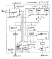
図1を参照すると、スーパースカラプロセッサ10の一実施例のブロック図が示されている。他の実施例が可能であり意図される。図1に示した実施例において、プロセッサ10は、プリデコードユニット12、L1 I−キャッシュ14、L0 I−キャッシュ16、フェッチ/スキャンユニット18、命令キュー20、アライメントユニット22、リネーム/スケジュールユニット24、第1のリネームレジスタファイル30A、第2のリネームレジスタファイル30B、複数の機能ユニット32A、32B、32C、32D、32Eおよび32F、複数のアドレス発生ユニット34A、34B、34Cおよび34D、ロード/ストアユニット36、L1 D−キャッシュ38、ならびに外部インターフェイスユニット42を含む。本明細書において特定の参照番号およびこれに続く種々の文字によって参照する構成要素はまとめてこの参照番号のみを用いて示す。たとえば、機能ユニット32A−32Fはまとめて機能ユニット32として示す。
【0020】
図1の実施例において、外部インターフェイスユニット42は、プリデコードユニット12、ロード/ストアユニット36、L2インターフェイス44およびバスインターフェイス46に結合される。プリデコードユニット12はさらにL1 I−キャッシュ14に結合される。L1 I−キャッシュ14は、L0 I−キャッシュ16およびフェッチ/スキャンユニット18に結合される。フェッチ/スキャンユニット18もL0 I−キャッシュ16および命令キュー20に結合される。命令キュー20はアライメントユニット22に結合されこれはさらにリネーム/スケジュールユニット24に結合される。リネーム/スケジュールユニット24はさらに、第1のリネームレジスタファイル30A、第2のリネームレジスタファイル30Bおよびロード/ストアユニット36に結合される。ロード/ストアユニット36はL1 D−キャッシュ38に結合される。第1のリネームレジスタファイル30Aは、機能ユニット32A−32Cおよびアドレス発生ユニット34A−34BならびにL1 D−キャッシュ38に結合される。同様に、第2のリネームレジスタファイル30Bは、機能ユニット32D−32Fおよびアドレス発生ユニット34C−34DならびにL1 D−キャッシュ38に結合される。アドレス発生ユニット34A−34DはL1 D−キャッシュ38に結合される。
【0021】
一般的に言えば、プロセッサ10は、スタックポインタレジスタのためのルックアヘッド値を発生してスタックポインタレジスタから生まれる依存性を取除くことを試みる。多くの命令はスタックポインタレジスタを固定値だけまたは命令に含まれる値だけ(例として即値フィールド)インクリメントまたはデクリメントする。プロセッサ10は、これら操作の累積効果の計算を、特定の命令に先立ち、その特定の命令に対応するスタックポインタレジスタのためのルックアヘッド値を計算するために行なう。好都合なことに、そのスタックポインタの値についてのみ他の命令に依存する命令は並列に実行される。プロセッサ10は、スタックポインタレジスタへの更新を見分けられないことがある。プロセッサ10は、このような更新を検出すると、見分けられない更新が完了するまで後続の命令をストールする。その後、ルックアヘッド値の発生が続けられる。
【0022】
スタックポインタレジスタへの更新のひとつのタイプとして、レジスタのインクリメントでもデクリメントでもなく、多くのコードシーケンスでよくあるものに、ベースポインタからスタックポインタへの(およびその逆の)転送命令がある。一般に、転送は、ソースロケーションからデスティネーションロケーションへの値のコピーである。このコピーに続いて、ソースロケーションおよびデスティネーションロケーション双方は、当初ソースロケーションに格納されていた値を格納する。プロセッサ10は、スタックポインタレジスタのためのルックアヘッド値発生を続行するまでに経過する時間を減じるために、上記の転送の性能を加速するように構成される。
【0023】
より具体的には、ベースポインタレジスタからスタックポインタレジスタへの転送が検出されると、プロセッサ10は、そのレジスタリネーミングメカニズムに信号で知らせ、ベースポインタおよびスタックポインタレジスタのためのリネームタグをスワップする(転送命令のデスティネーションのためのリネームレジスタの割当後)。(転送命令より前の)ベースポインタレジスタに対応するリネームレジスタが有効であれば(すなわちリネームレジスタがデスティネーションレジスタとして割当てられた命令が実行済み)、転送に続く更新されたスタックポインタレジスタの値はリネームレジスタから読出され、スタックポインタレジスタのためのルックアヘッド値発生は転送命令の実行前に続けられる。ベースポインタレジスタは一定に保たれ転送前にスタックアドレスを発生するためにベースとして用いられることが多いため、リネームレジスタ内の値は有効であることが多い。好都合なことに、性能は、転送命令の加速および転送命令に続くスタックポインタ依存命令の加速を通して向上する。
【0024】
転送命令はまだプロセッサ10内で実行される。しかしながら、転送命令のデスティネーションに割当てられたリネームレジスタは、当初の命令のソースレジスタに関連付けられている(タグがスワップされるため)。一般に、転送命令は、ソースリネームレジスタ(スワッピング後の当初の命令のデスティネーションアーキテクチャ上レジスタに関連する)を読出し、デスティネーションリネームレジスタ(スワッピング後の当初の命令のソースアーキテクチャ上レジスタに関連する)を更新することにより、完了する。転送命令の実行後、双方のリネームレジスタは同じ値を格納する。本明細書で述べる態様で転送命令を加速することは、ルックアヘッド値を発生しないプロセッサ10の実施例においてさえ有利である。ベースポインタが既に有効であることが多いため、転送に続く命令の早期スケジュールが可能である。(タグスワッピングのため。これは転送の実行前にスタックポインタレジスタが有効であることを示す。)本明細書では便宜上リネームタグの「スワッピング」という用語を用いる。一般に、レジスタリネームメカニズムは、ソースリネームレジスタをデスティネーションリネームレジスタに再割当することにより転送命令を加速する。この実施例では、転送命令のデスティネーションのために割当てられたリネームレジスタは、ソースレジスタに割当てられ(すなわちタグがスワップされる)、ソースレジスタを更新する。他の実施例では他のやり方でソースレジスタに対する更新を行なう。(たとえば転送に続いて同じリネームをソースおよびデスティネーションレジスタ双方に割当ててもよい。)
プリデコードユニット12は、外部インターフェイスユニット42がフェッチした命令バイトを受け、この命令バイトを、L1 I−キャッシュ14に格納する前にプリデコードする。プリデコードユニット12が発生するプリデコード情報も、L1 I−キャッシュ14に格納される。一般に、プリデコード情報は、命令の特徴の識別を助けるために与えられ、命令のフェッチおよび発行中は役立つが、フェッチおよび発行動作中迅速に発生することが難しい。本明細書で用いる「プリデコード」という用語は、命令をデコードし、命令キャッシュ(たとえばL1 I−キャッシュ14および/またはL0 I−キャッシュ16)においてデコードされている命令バイトともに後で格納されるプリデコード情報を発生することを指す。
【0025】
ある実施例において、プロセッサ10は、1命令バイトにつき2ビットのプリデコード情報を用いる。「スタートビット」と呼ばれる、これらビットのうち一方は、命令バイトが命令の最初のバイトかどうかを示す。命令バイトのグループがフェッチされたとき、対応するスタートビットの組は、命令バイトのグループ内の命令間の境界を識別する。したがって、複数命令を、対応するスタートビットをスキャンすることにより、命令バイトのグループから同時に選択できる。スタートビットは、各命令の最初のバイトを識別することによって命令の境界の場所を示すのに用いられるが、その代わりにエンドビットを用いて各命令の最終バイトを識別することによって命令の境界の場所を示すことができる。
【0026】
この実施例で用いる、「制御転送」ビットと呼ばれる第2のプリデコードビットは、どの命令が分岐命令かを識別する。命令の先頭バイトに対応する制御転送ビットは、命令が分岐命令かどうかを示す。命令の後続バイトに対応する制御転送ビットは、小偏位フィールドの相対分岐命令を除き、ドントケアである。ある特定の実施例に従うと、小偏位フィールドは8ビットフィールドである。一般に、「小偏位フィールド」とは、分岐命令が発生するターゲットアドレスよりもビットの少ない偏位フィールドのことをいう。小偏位フィールドの相対分岐命令に対し、偏位バイトに対応する制御転送ビットを以下で述べるように用いる。
【0027】
プリデコードユニット12は、命令バイトに対応するプリデコード情報の発生に加え、この実施例においては相対分岐命令の偏位フィールドを再コード化して実際にターゲットアドレスを格納するように構成される。言い換えれば、プリデコードユニット12は、相対分岐命令の偏位を、プロセッサ10が用いる命令セットが定める相対分岐命令に対応するアドレスに加える。その結果得たターゲットアドレスは、偏位に置換わるものとして偏位フィールドにエンコードされ、更新された偏位フィールドは、元の偏位フィールドの代わりにL1 I−キャッシュ14に格納される。ターゲットアドレス発生は相対ターゲットアドレスを予め計算することにより簡略化され、こうして分岐予測メカニズムはより効率的に働く。
【0028】
x86命令セットを用いるプロセッサ10のある実施例において、プリデコードユニット12は、8ビットおよび32ビットの偏位フィールドを再コード化するように構成される。32ビット偏位フィールドは、ターゲットアドレスの全体を格納する。他方、8ビット偏位フィールドはエンコードされる。より具体的には、8ビット偏位フィールドおよび対応の制御転送プリデコードビットは、キャッシュラインオフセット部および相対キャッシュライン部に分割される。キャッシュラインオフセット部は、ターゲットアドレスのキャッシュラインオフセット部である。相対キャッシュライン部は、相対分岐命令を格納するキャッシュラインの上または下にあるキャッシュラインの数に関し、ターゲットアドレス(「ターゲットキャッシュライン」)が識別するキャッシュラインを定める。第1のキャッシュラインが第2のキャッシュラインよりも上にあるとは、第1のキャッシュライン内の各バイトが、第2のキャッシュライン内のバイトが格納されるアドレスよりも数値的に大きなアドレスに格納されている場合のことをいう。逆に、第1のキャッシュラインが第2のキャッシュラインよりも下にあるとは、第1のキャッシュライン内の各バイトが、第2のキャッシュライン内のバイトが格納されるアドレスよりも数値的に小さなアドレスに格納されている場合のことをいう。符号付き8ビット偏位は、分岐命令に対応するアドレスの+/−128バイトであるアドレスを特定する。したがって、8ビット偏位を有する相対分岐命令が到達可能な上下キャッシュライン数は限定される。相対キャッシュライン部は、この限定された上下キャッシュラインの組をエンコードする。
【0029】
以下の表1および2は、プロセッサ10のある実施例に従う、1バイトに対応するプリデコード情報のエンコードの例を示す。
【0030】
【表1】

【表2】
プリデコードユニット12は、受けた命令バイトおよび対応するプリデコード情報を格納するためにL1 I−キャッシュ14に送る。L1 I−キャッシュ14は、命令バイトおよびプリデコード情報を格納するための高速キャッシュメモリである。L1 I−キャッシュ14は、ダイレクトマップトおよびセットアソシアティブ構成を含む、何らかの適切な構成を用いる。ある特定の実施例では、L1 I−キャッシュ14は、128KBのツーウェイセットアソシアティブキャッシュであり64バイトのキャッシュラインを用いる。L1 I−キャッシュ14は、格納された命令バイトに対応するプリデコード情報のためのさらなる記憶部を含む。さらなる記憶部は、命令バイト記憶部と同様に編成される。本明細書で用いる「キャッシュライン」という用語は、特定のキャッシュ内の記憶部の割当の単位のことである。一般に、1キャッシュライン内のバイトをそのキャッシュは1単位として操作する(すなわち割当および割当解除を行なう)。
【0033】
ある実施例において、L1 I−キャッシュ14は、線形的にアドレス指定されかつ物理的にタグ付けされる。キャッシュが線形的にアドレス指定されるとは、キャッシュをインデックスするために用いるアドレスビットのうち少なくとも1つが、後に物理アドレスビットに変換される線形アドレスビットであることをいう。線形的にアドレス指定され/物理的にタグ付けされるキャッシュのタグは、インデックスに使用しないビットに加え変換された各ビットを含む。x86アーキテクチャで定められているように、命令は、セグメンテーション変換メカニズムを通して線形アドレスに変換されさらにページ変換メカニズムを通して物理アドレスに変換される論理アドレスを発生するように定められる。フラットアドレスモードを採用することがより一般的になりつつある。このフラットアドレスモードでは、論理アドレスおよび対応する線形アドレスは等しい。プロセッサ10はフラットアドレスモードを備えるように構成できる。したがって、命令の実行により発生するフェッチアドレス、ターゲットアドレスなどは線形アドレスである。L1 I−キャッシュ14においてヒットの検出があるかどうかを判断するために、フェッチ/スキャンユニット18が提示する線形アドレスを、トランスレーションルックアサイドバッファ(TLB)を用いて対応する物理アドレスに変換し、これをインデックスされたキャッシュラインからの物理タグと比較してヒット/ミスを判断する。フラットアドレスモードを用いないとき、プロセッサ10は依然としてコードを実行するが、さらなるクロックサイクルを用いて論理アドレスから線形アドレスを発生することができる。
【0034】
L0 I−キャッシュ16も、命令バイトを格納するための高速キャッシュメモリである。L1 I−キャッシュ14は大きいため、L1 I−キャッシュ14のアクセスタイムも長い。ある特定の実施例において、L1 I−キャッシュ14は2クロックサイクルのアクセスタイムを用いる。単一サイクルフェッチアクセスができるように、L0 I−キャッシュ16を用いる。L0 I−キャッシュ16は、L1 I−キャッシュ14と比較して小さく、したがってより高速のアクセスタイムをサポートできる。ある特定の実施例では、L0 I−キャッシュ16は、512バイトのフルアソシアティブキャッシュである。L1 I−キャッシュ14と同様、L0 I−キャッシュ16は、命令バイトのキャッシュラインおよび対応するプリデコード情報を格納するように構成される。(たとえば512バイトは8つの64バイトキャッシュラインを格納し、対応するプリデコードデータはさらなる記憶部に格納される。)ある実施例において、L0 I−キャッシュ16は、線形的にアドレス指定されかつ線形的にタグ付けされる。
【0035】
フェッチ/スキャンユニット18は、L0 I−キャッシュ16のためのフェッチアドレスおよびL1 I−キャッシュ14のためのプリフェッチアドレスを発生するように構成される。L0 I−キャッシュ16からフェッチされた命令をフェッチ/スキャンユニット18がスキャンすることにより、ディスパッチのための命令を識別し、かつ、分岐命令の場所を示し、場所が示された分岐命令に対応する分岐予測を形成する。命令スキャン情報および対応する命令バイトを、フェッチ/スキャンユニット18が命令キュー20に格納する。さらに、識別された分岐命令および分岐予測を用いて、L0 I−キャッシュ16のための後続フェッチアドレスを発生する。
【0036】
フェッチ/スキャンユニット18は、プリフェッチアルゴリズムを用いて、L1 I−キャッシュ14からL0 I−キャッシュ16へのキャッシュラインのプリフェッチを、フェッチ/スキャンユニット18がプロセッサ10へのディスパッチのためにプリフェッチされたキャッシュラインをフェッチする前に、行なおうとする。いかなる適切なプリフェッチアルゴリズムを用いてもよい。ある実施例において、フェッチ/スキャンユニット18は、特定のクロックサイクル中、(i)分岐予測誤りが信号で知らされる、(ii)L0 I−キャッシュミスが検出される、または(iii)L0 I−キャッシュ16でミスが発生すると想定されるターゲットアドレスが発生される、といった事態が発生しない限りは、L0 I−キャッシュ16からフェッチしたキャッシュラインに対してシーケンシャルな次のキャッシュラインをプリフェッチするように構成される。ある特定の実施例において、32ビット偏位を用いる相対分岐命令および間接ターゲットアドレス発生を用いる分岐命令は、L0 I−キャッシュ16でミスを発生させると想定される。(i)の場合、フェッチ/スキャンユニット18は、訂正済のフェッチアドレスに対してシーケンシャルなキャッシュラインをプリフェッチする。(ii)および(iii)の場合、フェッチ/スキャンユニット18は、対応するミスまたはターゲットアドレスをプリフェッチする。
【0037】
フェッチ/スキャンユニット18は、1クロックサイクル中に、より大きな命令の「ラン」をフェッチしようと、攻撃的な分岐予測メカニズムを用いる。本明細書で用いる、命令の「ラン」とは、1以上の命令の組であり、この組内で特定されるシーケンス内で実行されると予測される。たとえば、フェッチ/スキャンユニット18は、L0 I−キャッシュ16から24命令バイトのランをフェッチする。各ランは、数個のセクションに分割され、これをフェッチ/スキャンユニット18が並列にスキャンして、分岐命令を識別し、命令キュー20のための命令スキャン情報を発生する。ある実施例に従うと、フェッチ/スキャンユニット18は、大きな命令のランをサポートするために、1クロックサイクル当たり2つまでの分岐命令を予測しようとする。
【0038】
命令キュー20は、後続のディスパッチのためにフェッチ/スキャンユニット18が与える命令バイトを格納するように構成される。命令キュー20は、先入れ先出し(FIFO)バッファとして動作する。ある実施例において、命令キュー20は、複数のエントリを格納するように構成される。各エントリは、命令のラン、ランの各セクション内の5つまでの命令を識別するスキャンデータ、および、ランの各セクションに対応するアドレスを含む。さらに、命令キュー20は、アライメントユニット22に提示するために、4つまでの連続ランセクション内の6つまでの命令を選択するように構成される。命令キュー20は、例として2から3のエントリを用いる。命令キュー20の一実施例に関する詳細をさらに以下で示す。
【0039】
アライメントユニット22は、命令キュー20が識別した命令を、リネームスケジュールユニット24内の1組の発行位置まで送るように構成される。言い換えれば、アライメントユニット22は、命令キュー20が与えるスキャン情報に応答し、命令キュー20が与えるランセクションから、各命令を形成するバイトを選択する。命令は、プログラム順で発行位置に与えられる。(すなわちプログラム順で最初の命令は第1の発行位置に与えられ、プログラム順で2番目の命令は第2の発行位置に与えられるというふうに行なわれる。)
リネーム/スケジュールユニット24は、レジスタリネーミングおよび命令スケジューリング機能をもたらす。より具体的には、リネーム/スケジュールユニット24は、各命令のソースレジスタのための現在のリネームタグを与え、かつ、リネームタグを各命令のデスティネーションレジスタに割当てる。リネームタグは、リネームレジスタファイル30A−30B内のリネームレジスタを識別する。
【0040】
さらに、リネーム/スケジュールユニット24は、あるタイプの命令のためのルックアヘッド値を発生しようとする。ルックアヘッド値発生は、x86命令セットを用いる実施例にとっては特に有益である。x86命令セットの性質のため、典型的なコードシーケンス内の命令の多くは、単純な転送の類である。この特徴の理由のひとつは、x86命令は2つのオペランドを含み、そのどちらもソースオペランドであり、このうち一方がデスティネーションオペランドだということである。したがって、各命令のソースオペランドのうち一方が実行結果で上書される。さらに、x86命令セットが特定する、レジスタオペランドの格納のためのレジスタはほとんどない。したがって、多くの命令はメモリ内に保持されるスタックへのまたこのスタックからのオペランドの転送である。さらに、多くの命令依存性はESP/EBPレジスタに対する依存性であるが、これらレジスタに対する更新の多くは以前に格納された値のインクリメントおよびデクリメントである。これらの命令の実行を加速するために、リネーム/スケジュールユニット24は、1クロックサイクル中にデコードされる各命令に対しESPレジスタのルックアヘッドコピーを発生する。
【0041】
命令および割当てられたリネームは、リネーム/スケジュールユニット24内のスケジューラに格納される。命令のためのソースオペランドが利用できるようになると(すなわちリネームレジスタファイル30A−30Bに書込まれる)、命令は特定の機能ユニット32A−32Fによる実行のためにスケジュールされる。
【0042】
リネームレジスタファイル30A−30Bは、命令が実行のためにスケジュールされると、これらの命令をリネーム/スケジュールユニット24から受ける。リネームレジスタファイル30A−30Bは、各命令のソースリネームタグに従いリネームレジスタを読出し、ソース値を、各命令の実行のために選択された機能ユニット32A−32Fまたはアドレス発生ユニット34A−34Dに与える。リネームレジスタファイル30A−30Bは、各機能ユニットからの実行結果(およびD−キャッシュ38からのロードメモリ演算結果)を、デスティネーションに割当てられたリネームタグとともに受ける。リネームレジスタファイル30A−30Bは、識別されたリネームレジスタに実行結果を格納する。リネームレジスタファイル30A−30Bは複数のリネームレジスタを含む。たとえば、リネームレジスタファイル30A−30Bは各々、100から200のリネームレジスタを含む。
【0043】
リネームレジスタファイル30A−30Bはミラーイメージとして保持される。リネームレジスタファイル30A−30Bは、単一のリネームレジスタファイルの代わりに設けられて、各レジスタファイルに設けられる読出ポートの数を減じる。書込ポートの数は同じままでよい(結果は一方のレジスタファイルから他方のレジスタファイルに伝搬されるため)。しかしながら、読出ポートの減少のためインプリメンテーションにおいてかなりの節約となる。(たとえば読出ポートの数は書込ポートの数の約2倍であることが多い。)これに応じて、リネームレジスタファイル30Aは、オペランドを機能ユニット32A−32Cおよびアドレス発生ユニット34A−34Bに与え、結果を機能ユニット32A−32CおよびD−キャッシュ38から受取る。同様に、リネームレジスタファイル30Bは、オペランドを機能ユニット32D−32Fおよびアドレス発生ユニット34C−34Dに与え、結果を機能ユニット32D−32FおよびD−キャッシュ38から受取る。リネームレジスタファイル30Aに与えられた結果はリネームレジスタファイル30Bに伝搬され、リネームレジスタファイル30Bに与えられた結果はリネームレジスタファイル30Aに伝搬される。ある実施例では、反対側のリネームレジスタファイルへの結果の伝搬は1クロックサイクルの遅延を伴う。
【0044】
x86命令セットを用いるプロセッサ10の実施例において、命令は、アドレス発生ユニット34およびロード/ストアユニット36のための暗黙のメモリ演算および機能ユニット32のための明示的な機能的演算を含む。メモリオペランドのない命令は、メモリ演算を含まず、機能ユニット32が処理する。ソースメモリオペランドおよびレジスタデスティネーションオペランドを有する命令は、アドレス発生ユニット34およびロード/ストアユニット36が処理する暗黙のロードメモリ演算ならびに機能ユニット32が処理する明示的な機能的演算を含む。メモリソース/デスティネーションオペランドを有する命令は、アドレス発生ユニット34およびロード/ストアユニット36が処理する暗黙のロードおよびストアメモリ演算ならびに機能ユニット32が処理する明示的機能演算を含む。最後に、明示的機能演算のない命令は、ロード/ストアユニット36が処理する。各メモリ演算により、アドレス発生ユニット34が扱うアドレス発生が生じる。本明細書ではメモリ演算および命令(すなわち機能演算)に別の呼称を与えているが、単一の命令から生じることもある。
【0045】
アドレス発生ユニット34は、アドレス発生演算を行なってメモリ演算のためのアドレスを発生するように構成される。発生したアドレスは、L1 D−キャッシュ38およびロード/ストアユニット36に転送される。ある実施例に従うと、アドレス発生ユニット34Aおよび34Cをロードメモリ演算のために用い、アドレス発生ユニット34Bおよび34Dをストアメモリ演算のために用いる。機能ユニット32Aおよび32Dは、整数算術/論理演算を行ないかつ分岐命令を実行するように構成された整数機能ユニットである。機能ユニット32Bおよび32Eは、マルチメディア命令を実行するように構成されたマルチメディア実行ユニットであり、機能ユニット32Cおよび32Fは、浮動小数点命令を実行するように構成された浮動小数点ユニットである。図示の実施例において、各機能ユニット32は、1クロックサイクル当たり適切なタイプの2つまでの命令を実行するように構成される。何らかの制限を適用してもよい(たとえば1クロックサイクル当たり整数乗算は1つのみ、1つの浮動小数点超越数など)。
【0046】
ロード/ストアユニット36は、L1 D−キャッシュ38のインターフェイスとなりストアメモリ動作のデータ記憶部分を実行しかつロード/ストア依存性チェックを処理するように構成される。メモリ演算は、データをプロセッサ10と外部メモリとの間で転送することである。このメモリ演算は、明示的な命令、または、機能ユニット32が実行する演算も含む命令の暗黙的な部分である。ロードメモリ演算は、外部メモリからプロセッサ10へのデータ転送を特定し、ストアメモリ演算は、プロセッサ10から外部メモリへのデータ転送を特定する。L1 D−キャッシュ38内でメモリ演算に対するヒットが検出された場合、メモリ動作は外部メモリへのアクセスなしでその中で終了する。
【0047】
L1 D−キャッシュ38は、データを格納するための高速キャッシュメモリである。L1 D−キャッシュ38に、セットアソシアティブおよびダイレクトマップト構成を含め何らかの適切な構成を用いることができる。ある特定の実施例において、L1 D−キャッシュ38は、64バイトラインを用いる128KBのツーウェイセットアソシアティブキャッシュである。L1 D−キャッシュ38をたとえば1ウェイ当たり32バンクのキャッシュメモリとして編成できる。加えて、L1 D−キャッシュ38は、L1 I−キャッシュ14と同様のTLBを用いる、線形的にアドレス指定され/物理的にタグ付けされるキャッシュでもよい。
【0048】
外部インターフェイスユニット42は、命令バイトおよびデータバイトのキャッシュラインを、キャッシュミスに応答してプロセッサ10に転送するように構成される。命令キャッシュラインはプリデコードユニット12に送られ、データキャッシュラインはL1 D−キャッシュ38に送られる。加えて、外部インターフェイスユニット42は、L1 D−キャッシュ38が廃棄したキャッシュラインを、廃棄されたキャッシュラインが既にプロセッサ10に修正されているならばメモリに転送するように構成される。図1に示すように、外部インターフェイスユニット42は、L2インターフェイス44を介して外部インターフェイスL2キャッシュへのインターフェイスとなり、バスインターフェイス46を介してコンピュータシステムへのインターフェイスとなるように構成される。ある実施例では、バスインターフェイスユニット46はEV/6バスインターフェイスを含む。
【0049】
次に図2を参照して、フェッチ/スキャンユニット18の一実施例のブロック図が示される。他の実施例が可能であり意図される。図2に示すように、フェッチ/スキャンユニット18は、プリフェッチ制御ユニット50、複数の次選択ブロック52A−52C、命令選択マルチプレクサ(mux)54、命令スキャナ56、分岐スキャナ58、分岐履歴テーブル60、分岐選択マルチプレクサ62、リターンスタック64、間接アドレスキャッシュ66、および転送まとめユニット68を含む。プリフェッチ制御ユニット50は、L1 I−キャッシュ14、L0 I−キャッシュ16、間接アドレスキャッシュ66、リターンスタック64、分岐履歴テーブル60、分岐スキャナ58、および命令選択マルチプレクサ54に結合される。次選択ブロック52AはL1 I−キャッシュ14に結合され、次選択ブロック52B−52CはL0 I−キャッシュ16に結合される。各次選択ブロック52は命令選択マルチプレクサ54に結合され、これはさらに分岐スキャナ58および命令スキャナ56に結合される。命令スキャナ56は命令キュー20に結合される。分岐スキャナ58は、分岐履歴テーブル60、リターンスタック64および分岐選択マルチプレクサ62に結合される。分岐選択マルチプレクサ62は間接アドレスキャッシュ66に結合される。分岐履歴テーブル60および分岐スキャナ58は転送まとめユニット68に結合され、これは命令キュー20に結合される。
【0050】
プリフェッチ制御ユニット50は、分岐スキャナ58、分岐履歴テーブル60、リターンスタック64および間接アドレスキャッシュ66から、(ターゲットアドレスおよびテイクン/ノットテイクン予測を含む)分岐予測情報を受ける。プリフェッチ制御ユニット50は、分岐予測情報に応答して、L0 I−キャッシュ16のためのフェッチアドレスおよびL1 I−キャッシュ14のためのプリフェッチアドレスを発生する。ある実施例において、プリフェッチ制御ユニット50は、L0 I−キャッシュ16のための2つのフェッチアドレスを発生する。第1のフェッチアドレスは、分岐スキャナ58が識別した第1の分岐命令(もしあれば)に対応するターゲットアドレスとして選択される。第2のフェッチアドレスは、以前のクロックサイクルにおいて選択されたフェッチアドレス(すなわち命令選択マルチプレクサ54が選択したランに対応するフェッチアドレス)に対するシーケンシャルアドレスである。
【0051】
L0 I−キャッシュ14は、この2つのフェッチアドレスに対応するキャッシュライン(およびプリデコード情報)ならびにこれらキャッシュライン各々に対してシーケンシャルなキャッシュライン(およびプリデコード情報)を与えて、次のブロック52B−52Cを選択する。より具体的には、次選択ブロック52Bはシーケンシャルアドレスに対応するシーケンシャルキャッシュラインおよびこのシーケンシャルキャッシュラインの次に続くキャッシュラインを受ける。次選択ブロック52Cは、ターゲットアドレスに対応するターゲットキャッシュラインおよびこのターゲットキャッシュラインにシーケンシャルなキャッシュラインを受ける。加えて、次選択ブロック52B−52Cは、対応するフェッチアドレスのオフセット部分を受ける。次選択ブロック52B−52Cは各々、受けたキャッシュラインから、命令バイトのラン(および対応するプリデコード情報)を選択する。これは、対応するフェッチアドレスのオフセット部分を含むランセクションで始まる。各フェッチアドレスのオフセット部分はキャッシュライン内のどこからでも始まり得るため、選択されたランは、フェッチされたキャッシュラインおよびフェッチされたキャッシュラインにシーケンシャルなキャッシュラインの一部を含むことがある。したがって、次選択ブロック52B−52Cは、フェッチされたキャッシュラインおよびシーケンシャルなキャッシュライン双方を受ける。
【0052】
同様に、次選択ブロック52Aは、L1 I−キャッシュ14からプリフェッチされたキャッシュライン(および対応するプリデコード情報)を受け、ここから命令ランを選択する。1つのキャッシュラインがL1 I−キャッシュ14からプリフェッチされるため、ここから選択されるランは、プリフェッチアドレスのオフセット部分がキャッシュラインの終端に近ければ、ラン全体よりも小さいかもしれない。なお、L0 I−キャッシュ16からのフェッチキャッシュラインは、プリフェッチ制御ユニット50が対応するアドレスを発生するのと同じクロックサイクルで与えられるが、プリフェッチキャッシュラインは、L1 I−キャッシュ14のサイズが大きくアクセスタイムが遅いために1クロックサイクル遅延するかもしれない。L1 I−キャッシュ14は、プリフェッチされたキャッシュラインを次選択ブロック52Aに与えることに加えて、プリフェッチされたキャッシュラインをL0 I−キャッシュ16に与える。プリフェッチされたキャッシュラインが既にL0 I−キャッシュ16内に格納されている場合、L0 I−キャッシュ16はプリフェッチされたキャッシュラインを廃棄する。しかしながら、プリフェッチされたキャッシュラインが既にL0 I−キャッシュ16に格納されているのでなければ、プリフェッチされたキャッシュラインはL0 I−キャッシュ16に格納される。この態様で、現在アクセスされているキャッシュラインは、L0 I−キャッシュ16にここからの高速アクセスのために与えられる。なお、ある特定の実施例で、L0 I−キャッシュ16はフルアソシアティブキャッシュとして編成される。所望に応じて他の編成を用いてもよい(たとえばダイレクトマップト、セットアソシアティブなど)。
【0053】
プリフェッチ制御ユニット50は、命令選択マルチプレクサ54を制御することにより、分岐予測情報に応答して、次選択ブロック52の1つから与えられる命令ランを選択する。以下でさらに詳細に説明するように、プリフェッチ制御ユニット50は、クロックサイクルの初期に分岐スキャナ58、リターンスタック64および間接アドレスキャッシュ66からターゲットアドレスを受け、かつ分岐スキャナ58が識別する第1の分岐命令のオペコードバイトの少なくとも一部を受ける。プリフェッチ制御ユニット50は、このオペコードバイトの一部をデコードし、種々のターゲットアドレスソースから、L0 I−キャッシュ16からフェッチされたターゲットアドレスを選択し、選択したターゲットアドレスをL0 I−キャッシュ16に与える。並行して、以前のクロックサイクルで選択されたフェッチアドレスに対するシーケンシャルアドレス(以前のクロックサイクルからの分岐予測次第で以前のクロックサイクルからのターゲットアドレスまたはシーケンシャルアドレスのいずれか)を計算してL0 I−キャッシュ16に与える。分岐予測情報(すなわちテイクンまたはノットテイクン)は、このクロックサイクルの後期に分岐履歴テーブル60が与える。L0 I−キャッシュ16からフェッチしたターゲットアドレスに対応する分岐命令がテイクンと予測されたならば、プリフェッチ制御ユニット50は、次選択ブロック52Cが提供する命令ランを選択する。逆に、分岐命令がノットテイクンと予測されたならば、次選択ブロック52Bが選択する命令ランが選択される。次選択ブロック52Aが提供する命令ランは、予測されたフェッチアドレスが以前のクロックサイクルにおいてL0 I−キャッシュ16でミスしL1 I−キャッシュ14からフェッチされた場合に選択される。加えて、分岐命令に応答してプリフェッチされた命令ランが32ビット偏位もしくは間接ターゲットアドレス発生を備える場合またはL0 I−キャッシュミスがフェッチされた場合に、L1 I−キャッシュ14からの命令ランが選択される。
【0054】
選択された命令ランは、命令スキャナ56および分岐スキャナ58に与えられる。命令スキャナ56は、選択された命令ランに対応するプリデコード情報をスキャンして、命令ラン内の命令を識別する。より具体的には、ある実施例において、命令スキャナ56は各ランセクションに対応するスタートビットを並列にスキャンし、各ランセクション内の5つまでの命令を識別する。識別された命令(ランセクション内のオフセット)へのポインタが発生される。ポインタ、命令バイトおよびアドレス(1ランセクションにつき1つ)は、命令スキャナ56によって命令キュー20に運ばれる。特定のランセクションが5を上回る命令を含む場合、その特定のランセクションに続くランセクションに対応する情報は無効化され、この特定のランセクションおよび後続のランセクションは次のクロックサイクル中に再スキャンされる。
【0055】
マイクロコードを用いる実施例については、マイクロコード命令が命令のデコード中に識別される(たとえば命令が発行された発行位置において直接デコードされた命令がないことにより)。
【0056】
分岐スキャナ58は、命令スキャナ56と並列に命令ランをスキャンする。分岐スキャナ58は、命令ランのスタートビットおよび制御転送ビットをスキャンして命令ラン内の最初の2つの分岐命令を識別する。上記のように、分岐命令は、セットされた命令のスタートバイト(スタートビットで識別される)に対応する制御転送ビットにより識別される。分岐スキャナ58は、最初の2つの分岐命令の場所がわかると、命令を相対分岐命令と仮定し、対応のエンコードされたターゲットアドレスを、分岐命令のスタートバイトに続く命令バイトから選択する。x86命令セットを用いる実施例については、9ビットターゲットアドレス(偏位バイトおよび対応する制御転送ビット)が選択され、32ビットターゲットアドレスも選択される。さらに、スタートおよび制御転送ビットが識別するオプコードバイトの少なくとも一部が選択される。ターゲットアドレスおよびオプコードバイトは、L0 I−キャッシュ16からのフェッチのためにターゲットアドレスを選択するのに用いるため、プリフェッチ制御ユニット50に送られる。各分岐命令のフェッチアドレス(各分岐命令を含むランセクションのフェッチアドレスおよびそのセクション内の分岐命令の位置から求められる)は、各分岐命令に対応するテイクン/ノットテイクン予測を選択するために分岐履歴テーブル60に送られる。さらに、各分岐命令に対応するフェッチアドレスは、分岐選択マルチプレクサ62に送られ、さらに間接アドレスキャッシュ66に送られる。各分岐命令のターゲットアドレスは、転送まとめユニット68に送られる。ある実施例に従うと、分岐スキャナ58は、最初の2つの分岐命令に対し各ランセクションを並列にスキャンし、スキャン結果を組合せてラン内の最初の2つの分岐命令を選択するように構成される。
【0057】
分岐スキャナ58はさらに、1クロックサイクル中にサブルーチン呼出命令がスキャンされるかどうかを判断するように構成される。分岐スキャナ58は、検出されたサブルーチン呼出命令に続く命令のフェッチアドレスを、リターンスタック64に、ここに格納するために転送する。
【0058】
ある実施例において、1つのラン内に2を上回る分岐命令がある場合、このランを再び後続のクロックサイクル中にスキャンして後続の分岐命令を識別する。
【0059】
識別された分岐命令のフェッチアドレスを分岐履歴テーブル60に与えて、各命令についてテイクン/ノットテイクン予測を判断する。分岐履歴テーブル60は、以前に検出された分岐命令の振舞いに対応する複数のテイクン/ノットテイクン予測子を含む。予測子のうち1つを、最新の予測の履歴を保存し、これら最新の予測と、分岐命令に対応するフェッチアドレスの一部との排他的論理和を計算することにより、選択する。最新から最も遠い(最も古い)予測と、フェッチアドレスの一部内の最上位ビットとの排他的論理和を計算し、同様の計算を続け、最新の予測とフェッチアドレスの一部内の最下位ビットとの排他的論理和の計算も含まれる。1クロックサイクルにつき2つの予測子が選択されるため、第2の分岐命令に対応する予測子は、第1の分岐命令の予測に依存する(対応するフェッチアドレスの最下位ビットとの排他的論理和のため)。分岐履歴テーブル60は、選択され得る予測子双方を選択し(すなわち第1の分岐命令がノットテイクンと予測された場合に選択されるであろう予測子および第1の分岐命令がテイクンと予測された場合に選択されるであろう予測子)、次に第1の分岐命令について選択された実際の予測に基づき2つの予測子のうち1つを選択することによって、第2の予測子を提供する。
【0060】
分岐履歴テーブル60は、分岐命令の実行に関する情報を、機能ユニット32A−32Dから受ける。実行された分岐命令に対応する最近の予測の履歴および実行された分岐命令のフェッチアドレスは、更新する予測子を選択するために与えられ、実行された分岐命令のテイクン/ノットテイクン結果も与えられる。分岐履歴テーブル60は、対応する予測子を選択し、テイクン/ノットテイクン結果に基づき予測子を更新する。ある実施例において、分岐履歴テーブルはバイモーダルカウンタを格納する。このバイモーダルカウンタは、最大および最小値で飽和する飽和カウンタである。(すなわちカウンタは最小値の後のデクリメントおよび最大値の後のインクリメントでは何ら変化しない。)分岐命令がテイクンの度に、対応するカウンタがインクリメントされ、分岐命令がノットテイクンの度に、対応するカウンタがデクリメントされる。カウンタの最上位ビットは、テイクン/ノットテイクン予測を示す(たとえば、セットならテイクン、クリアならノットテイクン)。ある実施例において、分岐履歴テーブル60は、64Kの予測子を格納し、16の最新予測の履歴を保持する。各クロックサイクルで、そのクロックサイクル中に選択された予測は履歴にシフトされ、最も古い予測が履歴から追出される。
【0061】
リターンスタック64を用いて、検出されたサブルーチン呼出命令に対応するリターンアドレスを格納する。リターンスタック64は、分岐スキャナ58からサブルーチン呼出命令のフェッチアドレスを受ける。呼出命令に続くバイトのアドレス(リターンスタック64に与えられるフェッチアドレスから計算される)は、リターンスタック64のトップに置かれる。リターンスタック64は、リターンスタックのトップに格納されたアドレスを、リターン命令が分岐スキャナ58およびプリフェッチ制御ユニット50によって検出された場合に、ターゲットアドレスとして選択するためにプリフェッチ制御ユニット50に与える。この態様で、各リターン命令は、ターゲットアドレスとして最も最近検出された呼出命令に対応するアドレスを受ける。一般に、x86命令セットにおいて、呼出命令は、呼出命令に対するシーケンシャルアドレスがx86アーキテクチャが定めるスタックの上に置かれることを特定する制御転送命令である。リターン命令は、スタックのトップからターゲットアドレスを選択する命令である。一般に、呼出およびリターン命令がコードシーケンス内のサブルーチンへの(それぞれ)進入および退出のために用いられる。呼出命令に対応するアドレスをリターンスタック64に置き、リターンスタック64のトップのアドレスをリターン命令のターゲットアドレスとして用いることにより、リターン命令のターゲットアドレスを正確に予測できる。ある実施例において、リターンスタック64は16のエントリを含み得る。
【0062】
間接アドレスキャッシュ66は、以前の間接分岐命令の実行に対応するターゲットアドレスを格納する。間接分岐命令に対応するフェッチアドレスおよび間接分岐命令の実行に対応するターゲットアドレスは、機能ユニット32A−32Dにより間接アドレスキャッシュ66に与えられる。間接アドレスキャッシュ66は、対応するフェッチアドレスが指示するターゲットアドレスを格納する。間接アドレスキャッシュ66は、分析選択マルチプレクサ62が(間接分岐命令の検出に応答して)選択したフェッチアドレスを受け、このフェッチアドレスが間接アドレスキャッシュ66にヒットした場合、対応するターゲットアドレスをプリフェッチ制御ユニット50に与える。ある実施例において、間接アドレスキャッシュ66は32のエントリを含み得る。ある特定の実施例に従うと、フェッチアドレスが間接アドレスキャッシュ66でヒットした場合、間接アドレスキャッシュ66からはターゲットアドレスは与えられない。その代わりとして、所望されればそこに格納されたターゲットアドレスの1つが「推測された」ターゲットアドレスとして選択される。
【0063】
ある実施例に従うと、プリフェッチ制御ユニット50は、L0 I−キャッシュ16からのフェッチのためのターゲットアドレスを、(i)分岐スキャナ58が識別する第1の分岐命令に対応する第1のエンコードされたターゲットアドレス、(ii)リターンスタック64が与えるリターンスタックアドレス、および(iii)シーケンシャルアドレスから選択する。プリフェッチ制御ユニット50は、第1の命令に対応するオペコードのデコードが命令が相対分岐命令であることを示す場合、第1のエンコードされたターゲットアドレスを選択する。デコードが命令がリターン命令であることを示す場合、リターンスタックアドレスが選択される。それ以外の場合、シーケンシャルアドレスが選択される。間接ターゲットアドレスおよび32ビット相対ターゲットアドレスは、L1 I−キャッシュ14からプリフェッチされる。これらのタイプのターゲットアドレスは、ターゲットアドレスがメモリ内の分岐命令近くにないときに用いられることが多いため、こうしたタイプのターゲットアドレスがL0 I−キャッシュ16内でヒットすることは稀である。加えて、第2の分岐命令がテイクンと予測され第1の分岐命令がノットテイクンと予測される、または、第1の分岐命令が命令ランにおいて第2の分岐命令を排除しない前方分岐の場合、ある実施例に従うと、第2の分岐予測に対応する第2のターゲットアドレスを、後続のクロックサイクル中ターゲットフェッチアドレスとして用いる。
【0064】
なお、エンコードされたターゲットアドレスが選択された場合、実際のターゲットアドレスはL0 I−キャッシュ16に提示される。プリフェッチ制御ユニット50は、可能な上/下ターゲットアドレス各々を予め計算し、エンコードされたターゲットアドレスに基づき正しいアドレスを選択するよう構成される。その代わりとして、プリフェッチ制御ユニット50は、どのL0 I−キャッシュ記憶場所が上および下キャッシュラインを格納しているかを記録し、タグ比較なしで記憶場所を直接選択してもよい。
【0065】
転送まとめユニット68は、選択された各分岐命令の命令ラン内のターゲットアドレスおよび位置、およびテイクン/ノットテイクン予測を受ける。転送まとめユニット68は、受けた予測に基づき、そのラン内のどの命令を削除すべきかを決定する。第1の分岐命令がテイクンと予測され後方分岐の場合(すなわち偏位が負である)、第1の分岐命令に続くすべての命令が削除される。第1の分岐命令がテイクンと予測され前方分岐であるが偏位が小さい場合(たとえば命令ラン内)、第1の分岐命令とターゲットアドレスとの間の命令が削除される。第2の分岐命令は、第1の分岐命令の予測に従うとまだそのラン内にあるならば、同じように処理される。ラン内の命令についての削除表示は、命令キュー20にセットされる。
【0066】
プリフェッチ制御ユニット50はさらに、L1 I−キャッシュ14から与えられるキャッシュラインで置換するためにL0 I−キャッシュ16内のキャッシュラインを選択するよう構成される。ある実施例では、プリフェッチ制御ユニット50は、最長時間未使用(LRU)置換アルゴリズムを用いる。
【0067】
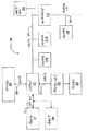
次に図3を参照して、リネーム/スケジュールユニット24のある実施例のブロック図が示される。他の実施例が可能であり意図される。図3の実施例において、リネーム/スケジュールユニット24は、FPスタック−絶対変換ユニット70、FPマップ72、ESPルックアヘッドユニット74、フューチャファイルリネームタグユニット76、アーキテクチャリネームタグユニット78、ルックアヘッド加算器80、スケジューラ82、結果キュー84、スケジューラ制御ユニット86、第1のピックコアユニット88、および第2のピックコアユニット90を含む。FPスタック−絶対変換ユニット70およびESPルックアヘッドユニット74は、アライメントユニット22に結合される。FPスタック−絶対変換ユニット70は、FPマップ72およびマルチプレクサ92に結合され、これはさらにアライメントユニット22およびフューチャファイルリネームタグユニット76に結合される。ESPルックアヘッドユニット74は、ルックアヘッド加算器80に結合され、これはさらに累積ESP更新を受けるようにスケジューラ82に結合される。ルックアヘッド加算器80およびフューチャファイルリネームタグユニット76は、スケジューラ82に結合される。フューチャファイルリネームタグユニット76はさらに、スケジューラ制御ユニット86およびアーキテクチャリネームタグユニット78に結合される。アーキテクチャリネームタグユニット78は、結果キュー84に結合され、これはさらにスケジュール制御ユニット86に結合される。第1および第2のピックコアユニット88および90は、スケジューラ82および第1および第2のリネームレジスタファイル30Aおよび30Bそれぞれに結合される。なお、1以上のデコードユニット(図示せず)を、並列にFPスタック−絶対変換ユニット70およびESPルックアヘッドユニット74に結合してもよく、または、これらユニットの前後に直列に結合して命令デコード動作を行なうようにしてもよい。
【0068】
上記のように、アライメントユニット22は、命令をリネーム/スケジュールユニット24内の1組の発行位置に整地する。発行位置は、スケジューラ82および結果キュー84内に保持される。命令を、スケジューラ82および結果キュー84に格納する前に、FPスタック−絶対変換ユニット70およびESPルックアヘッドユニット74に提示する。
【0069】
FPスタック−絶対変換ユニット70は、プロセッサ10の、浮動小数点レジスタがスタックとして動作する実施例のために与えられる(たとえばx86浮動小数点アーキテクチャ)。浮動小数点レジスタの1つは、浮動小数点状態レジスタにおけるスタックポインタのトップにより、スタックのトップとして識別され、他の浮動小数点レジスタは、スタックのトップが識別するレジスタからの相対距離に応じた、スタック内の位置にある。浮動小数点命令の中には、スタック内の1以上のエントリ上の演算を特定することに加えまたはその代わりに、ある値をスタックにプッシュすることまたはある値をスタックからポップすることを特定するものがある。FPスタック−絶対変換ユニット70は、浮動小数点命令に含まれるスタック相対レジスタ指定子を、絶対レジスタ指定子に変換する(すなわち浮動小数点レジスタファイルをアドレス指定するレジスタ番号)。FPスタック−絶対変換ユニット70は、変換を行なうために、以前にディスパッチされた浮動小数点命令に対応するスタックポインタの投機的トップを保持する。加えて、FPスタック−絶対変換ユニット70は、スタックポインタのトップに対する各浮動小数点命令の効果を、次の浮動小数点命令のためのレジスタ指定子を変換するために、求める。
【0070】
x86浮動小数点アーキテクチャはまた、2つのレジスタ内の値を交換する交換命令を特定する。FPスタック−絶対変換ユニット70は、レジスタ内の値を実際に交換する代わりに、2つの命令に対応する絶対レジスタ指定子をスワップすることにより、交換命令(およびそれに続く命令)を高速化する。FPマップ72はこのために設けられる。FPマップ72は、最初に、ゼロからN−1(たとえばx86アーキテクチャの0から7)の順で、絶対レジスタ番号を記録する。交換命令が実施されると、命令の影響を受ける絶対レジスタ指定子は、FPマップ72内でスワップされる。所与の浮動小数点命令に対する絶対レジスタ番号は、スタックポインタの現在の投機的なトップおよび特定されたレジスタのスタック内の位置により選択された、浮動小数点マップ72内のエントリを読出すことによって求められる(たとえば交換命令がない場合に絶対レジスタ指定子であったもの)。
【0071】
FPスタック−絶対変換ユニット70の出力は、マルチプレクサ(mux)92の一方入力に与えられる。元のレジスタ指定子は、マルチプレクサ92の他方入力に与えられる。各命令について、FPスタック−絶対変換ユニット70は、その出力または元の命令いずれかを、その命令が浮動小数点かどうかに基づき選択する。なお、交換命令は絶対レジスタ番号の順を変更するので、マルチメディア命令のレジスタ番号(絶対値である)は、x86マイクロプロセッサアーキテクチャを用いる実施例においてもFPスタック−絶対変換ユニット70により変換される。なお、さらに、オペコードおよび他の命令情報(たとえば即値フィールドおよび偏位フィールド)は、修正なしでマルチプレクサ82ならびにフューチャファイルおよびリネームタグユニット76を通して送られ、スケジューラ82に格納される。
【0072】
ESPルックアヘッドユニット74をルックアヘッド加算器80と組合せて用い、ESPをソースオペランドとする各命令についてESPレジスタのための投機的な値を発生する(x86アーキテクチャを用いるプロセッサ10の実施例で)。x86アーキテクチャが特定するレジスタは比較的少ないため、これらの多くは汎用ではなく、多くのx86命令はスタックオペランドを操作する。スタックオペランドの場所は、ESPレジスタをアドレスオペランドとして用いて求める。加えて、多くの命令はESPレジスタを修正する(たとえばプッシュおよびポップ値)。プッシュおよびポップ値は結果としてESPレジスタのインクリメントまたはデクリメントをもたらす。したがって、ESPレジスタに対する多くの修正は、予め、ESPレジスタに加算またはESPレジスタから減算する一定値として行なわれる。
【0073】
ESPルックアヘッドユニット74は、発行位置の組内にある命令をスキャンし、ESPルックアヘッドユニット74に与えられる発行位置の組内の第1の命令の実行前に存在するESPレジスタ値に加算される定数を発生する。これらの定数を、ESPレジスタの投機的ルックアヘッド値に加算し(プロセッサ10が以前にディスパッチした命令に対応する)、各命令についてESP値を発生する。言い換えれば、第1の発行位置(プログラム順で)に対して発生した定数は、第1の発行位置の命令の効果を含む(命令がESPをアドレスオペランドたとえばプッシュとして用いる前にそのESPを修正する場合)。第2の発行位置に対して発生した定数は、第1の発行位置の命令の効果および第2の発行位置の命令の効果を含む(命令がESPをアドレスオペランドたとえばプッシュとして用いる前にそのESPを修正する場合)。一般に、発行位置Nに対して発生した定数は、第1の発行位置から発行位置N−1における命令のESPに対する効果、および、発行位置Nにおける命令の効果を含む(命令がESPをアドレスオペランドたとえばプッシュとして用いる前にそのESPを修正する場合)。
【0074】
ESPルックアヘッドユニット72が発生する定数は、ルックアヘッド加算器80に与えられる。ルックアヘッド加算器80は、確定できない最後の更新以来投機的にディスパッチされた命令に従うESPレジスタに対する累積投機更新を示す累積ESP更新値を、保持する。ルックアヘッド加算器80は、ESPルックアヘッドユニット74から受けた定数を、ルックアヘッド加算器80が保持する累積ESP値に加算して、各命令についてルックアヘッドESP値を発生する。ESPルックアヘッドユニット74は、ESPに対するいくつかの更新(たとえば別のレジスタからESPへの転送、登録された値のESPへの加算など)を確定できない。ESPルックアヘッドユニット74は、このような確定不能の更新を検出した場合、この確定不能の更新を実行する命令の実行まで、この命令に続く命令をストールする。この更新をESP加算器80が受けて、投機的ルックアヘッドESP値の次の発生が行なえるようにする。ある実施例に従うと、ESPルックアヘッドユニット74は以下のx86命令のESPに対する更新を確定できる。すなわちCALL、RET 0,N、PUSH、POP、ADD ESP,IMM、ENTER 0,N、LEAVE 0,N、MOV EBP,ESP、およびMOV ESP,EBPである。
【0075】
マルチプレクサ92が選択したレジスタ指定子は、リネーミングのためにフューチャファイルリネームタグユニット76に送られる。フューチャファイルリネームタグユニット76は、各ソースレジスタに現在のリネームタグを与え、使用していないリネームレジスタのリストからの新規リネームレジスタを各デスティネーションレジスタに割当てる。フューチャファイルリネームタグユニット76はまた、並行してディスパッチされる命令間の依存性を解決する。最後に、フューチャファイルリネームタグユニット76は、リネームタグのフューチャファイルを更新して、新たに割当てられたリネームレジスタを表わす。
【0076】
リネームレジスタタグおよびルックアヘッド加算器80からのルックアヘッドESP値を含む命令は、格納のためにスケジューラ82に与えられる。ある実施例において、スケジューラ82は「ライン指向型」であり、ここには、命令および各発行位置からの関連情報を格納できる記憶ラインが、命令が各発行位置を占めていなくても、割当てられる。加えて、記憶部は、デスティネーションレジスタリネームタグを格納するために結果キュー84に割当てられる。
【0077】
命令は、スケジューラ82に格納されると、そのソースオペランドの有効性を待つ。有効になった時がその命令が実行のために選択されるのにふさわしい(「スケジュールされる」)時である。フューチャファイルリネームタグユニット76は、現在のリネームレジスタ(すなわち現在特定のアーキテクチャ上のレジスタに割当てられているレジスタ)である各リネームレジスタに対する有効表示を保持し、既に有効であるソースオペランドを有する命令は、スケジューラ82に格納されるとそれらのソースオペランドの有効性を示すであろう。無効であるリネームレジスタは、ソースオペランドがまだ有効でないことを示す(すなわちリネームレジスタを更新する命令の実行に応答して更新されていない)ため、命令はまだスケジュールに適していない。
【0078】
第1および第2のピックコアユニット88および90は、スケジュールに適したスケジューラ82内の命令、および、対応する第1および第2のコアへのスケジュール命令をそれぞれ調べる。第1のコアは、リネームレジスタファイル30Aに結びつけられた機能ユニットおよびアドレス発生ユニットを含み、同様に、第2のコアは、リネームレジスタファイル30Bに結びつけられた機能ユニットおよびアドレス発生ユニットを含む。第1および第2のピックコアユニット88および90が選択する命令は、オペランド読出のためにリネームレジスタファイル30Aおよび30Bに与えられ、スケジューラ制御ユニット86にも与えられる。
【0079】
スケジューラ制御ユニット86は、スケジュールされた各命令についてデスティネーションリネームレジスタを記録し、いつリネームレジスタが有効になるかを判断する。リネームレジスタが有効であると判断すると、リネームレジスタに対応するリネームタグはスケジューラにブロードキャストされる。ブロードキャストタグに合う各ソースレジスタリネームタグは有効であると示される。この実施例に従う整数、浮動小数点およびマルチメディア機能ユニットについて、リネームレジスタが有効になるまでのクロックサイクル数は、命令のタイプおよび命令により決まる定数である(たとえば乗算は加算よりも多くのクロックサイクルを含むなど)。メモリ演算は、キャッシュミスを含みしたがってスケジュールからリネーム有効までの可変の遅延を含むため、データキャッシュ38によりスケジューラ制御ユニット86に対し有効であるまたは有効でないと示される。スケジューラ制御ユニット86は、メモリ動作に対応するリネームタグの有効を、データキャッシュ38が有効と示すまで保留してもよい。
【0080】
スケジューラ制御ユニット86はまた、有効とされたレジスタリネームタグを、フューチャファイルリネームタグユニット76にブロードキャストし(フューチャファイルリネームタグユニット76はリネームタグをもしまだフューチャファイル内の現在のレジスタリネームならば有効と示す)、かつ、結果キュー84にブロードキャストする(結果キュー84は対応する命令の実行に成功したことを示す)。
【0081】
結果キュー84は、分岐予測誤り、ならびに他の例外処理および命令のインオーダリタイアを扱うために設けられる。命令のリタイアは、命令のデスティネーションに割当てられたリネームレジスタを識別するリネームタグを、アーキテクチャリネームタグユニット78に格納することにより行なう。結果キュー84は、命令のデスティネーションレジスタに割当てられたリネームタグおよびアーキテクチャ上のデスティネーションレジスタ番号を格納する。この態様で、リネームタグは、アーキテクチャリネームタグユニット78内の対応するアーキテクチャ上のレジスタと関連付けられる。このアーキテクチャ上のレジスタに対応する以前のリネームタグを未使用リストに戻す。加えて、結果キュー84は、機能ユニットから予測誤りリダイレクション/例外情報を受け、どの命令に例外が起こったのか判断する。誤って予測され別のタイプの例外が生じた命令のリタイアの際、結果キュー84は、アーキテクチャリネームタグ78に信号で知らせ、その内容をフューチャファイルリネームタグユニット76にコピーする。こうしてリネームタグのフューチャファイルは例外から回復する。なお、命令が、訂正された経路からフェッチされ、フューチャファイルリネームからアーキテクチャリネームへの復元前にフューチャファイルリネームタグユニット76に達するならば、命令は、例外発生命令および以前の命令のリタイアならびにフューチャファイルタグの回復までストールされる。なお、さらに、タグをスワップした転送命令のリタイアの際、転送命令に含まれる2つのレジスタのアーキテクチャ上のタグもスワップされる。
【0082】
ある実施例に従うと、命令ラインのスケジューラ82からの割当解除は、ライン内の全命令のスケジュールに成功したとき、または、予測誤りもしくは例外のためにラインの無効化が生じたときに行なわれる。命令のラインの結果キュー84からの割当解除は、リタイアの選択に際し、または予測誤りもしくは例外のための無効化に際して行なわれる。
【0083】
なお、種々の記憶デバイスが図2および3に示される(例としてデバイス79A、79Bおよび図2の同様のデバイス、デバイス79C、79Dおよび図3の同様のデバイス)。この記憶デバイスは、ラッチ、レジスタ、フリップフロップなどを表わしこれらを用いてパイプライン段を分離する。しかしながら、図2および3に示した特定のパイプライン段は、プロセッサ10の一実施例に適したパイプライン段の一実施例にすぎない。他の実施例では他のパイプライン段を用いることができる。
【0084】
次に図4を参照して、ESPルックアヘッドユニット74の一実施例のブロック図が示される。他の実施例が可能であり意図される。図4の実施例において、ESPルックアヘッドユニット74は、複数の定数発生器100A−100Fおよび分割移動検出ユニット102を含む。定数発生器100は、アライメントユニット22から命令を受けるように結合され、かつルックアヘッド加算器80に定数を与えるように結合される。加えて、分割移動検出ユニット102は、アライメントユニット22から命令を受けるように結合される。分割移動検出ユニット102は、分割制御バス104を介して分割制御情報を与え、かつスワップタグライン106を介してスワップタグ信号を与える。さらに、分割移動検出ユニット102は、ESPペンディングライン108でESPペンディング信号を受けるように結合される。
【0085】
分割移動検出ユニット102は、アライメントユニット22から与えられる命令をスキャンし、ベースポインタレジスタからスタックポインタレジスタへの(およびこの逆の)転送命令を検出するように構成される。このような命令を検出すると、分割移動検出ユニット102は、フューチャファイルタグユニット76へのスワップタグライン106上のスワップタグ信号をアサートする。フューチャファイルタグユニット76は、ESPルックアヘッドユニット74が処理している命令についてのリネームレジスタの割当に続いて、スタックポインタおよびベースポインタタグをスワップするように構成される。分割移動検出ユニット102は、タグのスワッピング後のESPペンディングラインの状態から、リネームレジスタファイル30におけるスタックポインタレジスタの新規の値が有効かどうか判断する。スタックポインタがまだペンディングの場合(すなわち有効でない)、分割移動制御ユニット102は、スタックポインタレジスタが有効になるまで後続の命令ディスパッチをストールする。スタックポインタレジスタが有効になると、ルックアヘッド加算器80は、スタックポインタレジスタの新規の値を、定数発生器100が発生する定数とともに用いるために読出す。
【0086】
この実施例において、分割移動検出ユニット102はさらに、定数発生器100が確定できないスタックポインタレジスタに対する更新を検出するように構成される。上記のある特定の実施例において、以下の命令に従うスタックポインタレジスタに対する更新は確定可能である。すなわちCALL、RET 0,N、PUSH、POP、ADD ESP,IMM、ENTER 0,N、LEAVE 0,N、MOV EBP,ESP、およびMOV ESP,EBPである。スタックポインタレジスタに対する他の更新は、分割移動検出ユニット102により検出される。このような確定不能の更新を検出すると、分割移動検出ユニット102は、確定不能の更新で、アライメントユニット22が与える1組の命令(「ライン」)を分割する。確定不能の更新を有する命令以前の命令は、ルックアヘッド加算器80およびフューチャファイルリネームタグユニット76にディスパッチされ、残りの命令は、確定不能の更新が完了するまでストールされる。ラインを分割したとき、分割移動検出ユニット102は、分割制御バス104を介して、アライメントユニット20、スケジューラ82およびフューチャファイルリネームタグユニット76に知らせる。分割が発生した命令が与えられ、分割発生を示す、アサートされた制御信号も与えられる。
【0087】
分割移動検出ユニット102は、ベースポインタースタックポインタ転送命令でもラインを分割する。命令はタグフューチャファイルにおけるタグのスワッピングにより加速されており、ルックアヘッド加算器80が保持する現在のルックアヘッド値は、ベースポインタースタックポインタ転送命令のディスパッチの際に無効になる。応じて、ラインが分割され、後続の命令が、新規スタックポインタリネームレジスタが有効になるまでストールされる。新規スタックポインタリネームレジスタは既に有効かもしれない。その場合、ストールされず新規の値が読出される、または、値が有効になり読出すことができるようになるまでストールされる。
【0088】
なお、この実施例では、スタックポインタレジスタからベースポインタレジスタへの転送もタグのスワッピングによって検出および処理する。しかしながら、スタックポインタレジスタは実際命令によって修正されないため、スタックポインタルックアヘッド値は無効にならない。したがって、この場合ラインは分割されない。しかしながら、簡単にするため、ベースポインタからスタックポインタへの転送も同じライン内にある場合は、ある実施例に従うと、ラインはスタックポインタからベースポインタへの転送で分割される。
【0089】
各定数発生器100A−100Fは、アライメントユニット22が整地した命令の発行位置の1つに対応し、ラインの、その発行位置以前の命令のESPに対する累積更新を示す定数を発生する。したがって、定数発生器100A(発行位置0に対する定数を発生する)は、発行位置0内の命令をスキャンする。定数発生器100Bは、発行位置0および1内の命令をスキャンする。これ以外も同様である。定数発生器100Fは2つの定数を発生する。第1の定数は発行位置5内の命令に対応し、第2の定数は1組の命令の累積更新を示す。定数発生器100Fが発生する第1および第2の定数は、発行位置5内の命令がESPの値をソースとして用い、値をインクリメントまたはデクリメントしてESPレジスタにデスティネーションとして格納する(たとえばPOP)場合は異なる。その代わりとして、累積定数を別に発生してもよい(たとえば分割移動検出ユニット102により)。
【0090】
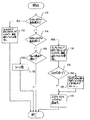
次に図5を参照して、分割移動検出ユニット102がアライメントユニット22から与えられる1組の命令をスキャンする一実施例の動作を示すフローチャートを示す。他の実施例が可能であり意図される。図5に示したステップは、理解しやすくするために直列順序で表わしているが、これらステップは何らかの適切な順序で実施できる。さらに、これらステップは、分割移動検出ユニット102内の組合せ論理において種々の並列形式で実施できる。
【0091】
分割移動検出ユニット102がスタックポインタからベースポインタへの転送を検出した場合(判断ブロック110)、分割移動検出ユニット102は、フューチャファイルリネームタグユニット76に信号で知らせ、ベースポインタおよびスタックポインタタグをスワップする(ステップ112)。加えて、分割移動検出ユニット102は、転送命令でラインを分割し、そのラインに対する処理は現在のクロックサイクルで終了する。分割に続く命令は再び次のクロックサイクルでアライメントユニット22により与えられる。
【0092】
同様に、分割移動検出ユニット102がベースポインタからスタックポインタへの転送を検出した場合(判断ブロック114)、分割移動検出ユニット102は、フューチャファイルリネームタグユニット76に信号で知らせ、ベースポインタおよびスタックポインタタグをスワップする(ステップ116)。加えて、分割移動検出ユニット102は、転送命令でラインを分割し、このラインに対する処理は現在のクロックサイクルで終了する。分割に続く命令は、次のクロックサイクル中にアライメントユニット22により与えられる。加えて、分割移動検出ユニット102は、タグスワップに続きフューチャファイルリネームタグユニット76からのESPペンディング信号を調べる(たとえばある特定の実施例では後続のクロックサイクルで)。スタックポインタタグがペンディングの場合(判断ブロック118)、分割移動検出ユニット102は、スタックポインタリネームレジスタ(すなわち前のベースポインタリネームレジスタ)が有効になるまで、後続の命令をストールする(ステップ120)。その後、スタックポインタレジスタの新規の値がリネームレジスタファイル30から読出される(ステップ122)。明確にするためにステップ122はこのフローチャートに含まれているが、この実施例においてステップ122はルックアヘッド加算器80が実施するものである。
【0093】
分割移動検出ユニット102はまた、異なる分割ライン条件を検出する(判断ブロック124)。たとえば、ESPに対する、他の確定不能の更新を検出する。さらに、並行してディスパッチされる命令に対する他の制限をこのやり方で検出する。このような制限は、プロセッサ10内のハードウェアをこうした限定を用いることで簡略化できるのであれば望ましい。異なる分割ライン条件を検出すると、分割移動検出ユニット102は識別された命令でラインを分割し、このラインに対する処理は終了する(ステップ126)。
【0094】
他方、上記のような条件が検出されなければ、ラインは次のパイプライン段に進み、分割移動検出ユニット102は、アライメントユニット22からの次のラインを待つ。
【0095】
次に図6を参照して、分割移動検出ユニット102のある実施例で用いるステートマシンの例が示される。他の実施例が可能であり意図される。たとえば、他の実施例では、これらが含まれるプロセッサのパイプラインに応じて異なるステートマシンを用い、または全く用いないこともある。図6の実施例では、正常状態150およびチェック状態152が設けられる。
【0096】
分割ライン条件の検出前、分割移動検出ユニット102は正常状態150にある。正常状態150で、分割移動検出ユニット102は、ステップ110、112、114、116、124および126を実施する。ベースポインタからスタックポインタへの転送が検出されない場合、分割移動検出ユニット102は状態150に留まる(アーク154)。他方、ベースポインタからスタックポインタへの転送が検出されれば、分割移動検出ユニット102は状態152に移る(アーク156)。加えて、スタックポインタおよびベースポインタリネームタグがスワップされる。
【0097】
チェック状態152で、分割移動検出ユニット102は、ステップ118および120を実行する(適切な応答をステップ118から受けた際)。タグのスワッピング後、スタックポインタレジスタがペンディングならば、分割移動検出ユニット102は状態152に留まる(アーク160)。加えて、後続命令がストールされる。スタックポインタレジスタが有効であれば、分割移動検出ユニット102は正常状態150に移る(アーク158)。
【0098】
次に図7を参照して、フューチャファイルリネームタグユニット76が保持するリネームタグおよび転送命令の検出時に行なうこれらのスワッピングを表わした例が示される。リネームレジスタ22を示すスタックポインタレジスタ(参照番号130)およびリネームレジスタ28を示すベースポインタレジスタ(参照番号132)に対応するリネームタグの初期状態が示されている。ベースポインタからスタックポインタへの転送命令が検出され(参照番号134)、命令のデスティネーションレジスタに割当てられたリネームレジスタはリネームレジスタ5である。
【0099】
転送命令のディスパッチに続き、スタックポインタ(参照番号136)に対応するリネームタグはリネームレジスタ28を示す(すなわち以前にベースポインタレジスタに割当てられたリネームレジスタ)。加えて、転送命令のディスパッチ後ベースポインタに対応するリネームタグ(参照番号138)はリネームレジスタ5を示す。
【0100】
図7の例は、ルックアヘッドスタックポインタ値の発生を加速するための、このタグスワッピング方法の利点の1つも示している。リネームレジスタ5はペンディングである(転送命令実行までペンディングである)が、リネームレジスタ28は有効である。したがって、スタックポインタレジスタに対応するルックアヘッド値を、リネームレジスタファイル30内のリネームレジスタ28を読出すことによって、迅速に回復できる。
【0101】
図7には、MOV ESP,EBP命令に応答してスケジューラに送られる転送命令も示される。この命令はMOV5,28(すなわちリネームレジスタ28内の値のリネームレジスタ5への転送)である。したがって、転送命令を実行すると、ベースポインタレジスタに割当てられたリネームレジスタは更新され、ペンディング表示はリセットされる。
【0102】
次に図8を参照して、フューチャファイルリネームタグユニット76が保持するリネームタグおよび転送命令の検出時のこれらのスワッピングを表わす別の例が示される。リネームレジスタ22を示すスタックポインタレジスタ(参照番号130)およびリネームレジスタ28を示すベースポインタレジスタ(参照番号132)に対応するリネームタグの初期状態が示される。スタックポインタからベースポインタへの転送命令が検出され(参照番号140)、命令のデスティネーションレジスタに割当てられたリネームレジスタはリネームレジスタ5である。
【0103】
転送命令のディスパッチ後、ベースポインタ(参照番号144)に対応するリネームタグはリネームレジスタ22を示す(すなわち以前にスタックポインタレジスタに割当てられたリネームレジスタ)。加えて、転送命令のディスパッチ後スタックポインタに対応するリネームタグ(参照番号142)は、リネームレジスタ5を示す。
【0104】
図8に示した例は、スタックポインタレジスタが現在ペンディングであることを示しているが、スタックポインタレジスタのルックアヘッドコピーは有効なままである。したがって、命令ディスパッチおよびスタックポインタレジスタのルックアヘッドコピーは引続き発生する。言い換えれば、分割移動検出ユニット102は、スタックポインタからベースポインタへの転送命令のためにタグスワップを実行するときにはESPペンディング信号を無視する。
【0105】
図8には、MOV EBP,ESP命令に応答してスケジューラに運ばれる転送命令も示される。この命令はMOV 5,22(すなわちリネームレジスタ22内の値のリネームレジスタ5への転送)である。したがって、この転送命令を実行すると、スタックポインタレジスタに割当てられたリネームレジスタは更新され、ペンディング表示はリセットされる。
【0106】
なお、図7および8の例は、ベースポインタレジスタおよびスタックポインタレジスタ対し1つのリネームタグを示しているが、実施例によっては各レジスタに対し複数のタグを用いてもよい。その場合、レジスタの一部は更新され他の部分は一定のままである(たとえばx86マイクロプロセッサアーキテクチャにおけるESPおよびSPまたはEBPおよびDP)。
【0107】
次に図9を参照して、命令キュー20の実施例のブロック図が示される。他の実施例が可能であり意図される。図9の実施例で、命令キュー20は、ラン記憶部300A−300B、スキャンデータ記憶部302A−302Bおよびアドレス記憶部304A−304Bを含む。加えて、命令キュー20は、マルチプレクサ306および制御ユニット308を含む。命令のランが、ランバス310を介してフェッチ/スキャンユニット18から命令キュー20に与えられ、対応するスキャンデータがスキャンデータバス312で与えられ、対応するアドレス(1ランセクション当たり1つ)がランアドレスバス314で与えられる。命令キュー20は、選択された1組の命令バイトを命令バイトバス316でアライメントユニット22に与え、ポインタを命令ポインタバス318で命令バイト内の命令に与え、選択された1組の命令バイトを含むランセクションに対するアドレスをアドレスバス320で与える。ランバス310はラン記憶部300A−300Bに結合され、スキャンデータバス312はスキャンデータ記憶部302A−302Bに結合され、アドレス記憶部304A−304Bはランアドレスバス314に結合される。記憶部300A−300B、302A−302Bおよび304A−304Bはマルチプレクサ306に結合され、これはさらにバス316−320に結合される。制御ユニット308はマルチプレクサ306およびスキャンデータ記憶部302A−302Bに結合される。
【0108】
フェッチ/スキャンユニット18、より具体的には図2の実施例に従う命令スキャナ56は、バス310−314を介し、命令キュー20に、命令のランおよび関連情報を与える。制御ユニット308は、この命令ランを含む命令バイトに対してラン記憶部300A−300Bのうちひとつを割当て、関連情報に対して対応するスキャンデータ記憶部302A−302Bおよびアドレス記憶部304A−304Bを割当てる。スキャンデータは、(i)ランセクション内のオフセットとしてのスタートバイトおよびエンドバイト、ならびに(ii)命令の存在するランセクションを識別する命令ポインタを含む。ある特定の実施例に従うと、8バイトのランセクション内で5つまでの命令を識別でき、スキャンデータ記憶部302に格納された合計で15までの命令ポインタに対するひとつのランに3つまでのランセクションがある。加えて、アドレス記憶部304は各ランセクションに対応するアドレスを格納する。
【0109】
制御ユニット308は、スキャンデータ記憶部302A−302B内の命令ポインタを調べ、アライメントユニット22にディスパッチするために、1組の連続するランセクション内の命令を識別する。ある特定の実施例では、4つまでの連続ランセクション内で6つまでの命令を識別する。ランセクションは、ラン記憶部300Aまたは300Bの1つに格納され、または、いくつかのランセクションがラン記憶部300A−300Bの一方から選択され、他のランセクションがラン記憶部300A−300Bの他方から選択される。第1のランセクションは、第1のランセクションが投機的プログラム順で第2のランセクションの次であれば、第2のランセクションに連続する。なお、マルチプレクサ306は図13で図面を簡単にするために1つのマルチプレクサとして示されているが、適切な並列または縦続接続されたマルチプレクサの組として実現してもよい。
【0110】
制御ユニット308は、1組の選択信号をマルチプレクサ306に与えて、選択された命令を含むランセクションの組および選択された命令に対応する命令ポインタを選択する。加えて、選択された各ランセクションに対するアドレスが選択される。ランセクションは命令バイトバス316上に出力され、対応する命令ポインタおよびアドレスはそれぞれ命令ポインタバス318およびアドレスバス320上に出力される。
【0111】
図10を参照して、バスブリッジ202を通して種々のシステム構成要素に結合されるプロセッサ10を含むコンピュータシステム200の一実施例のブロック図が示される。他の実施例が可能であり意図される。図示のシステムでは、メインメモリ204がメモリバス206を通してバスブリッジ202に結合され、グラフィックスコントローラ208がAGPバス210を通してバスブリッジ202に結合される。最後に、複数のPCIデバイス212A−212BがPCIバス214を通してバスブリッジ202に結合される。セカンダリバスブリッジ216をさらに設け、EISA/ISAバス220を通して1以上のEISAまたはISAデバイス218への電気的インターフェイスとしてもよい。
【0112】
バスブリッジ202は、プロセッサ10、メインメモリ204、グラフィックスコントローラ208およびPCIバス214に結びつけられたデバイス間のインターフェイスを提供する。バスブリッジ202に接続されたデバイスの1つからのオペレーションを受けると、バスブリッジ202はそのオペレーションのターゲットを識別する(たとえば特定のデバイス、またはPCIバス214の場合、ターゲットはPCIバス214上にある)。バスブリッジ202は、このオペレーションをターゲットデバイスに送る。バスブリッジ202は一般に、オペレーションを、ソースデバイスまたはバスが用いるプロトコルから、ターゲットデバイスまたはバスが用いるプロトコルに変換する。
【0113】
PCIバス214のためのISA/EISAバスへのインターフェイスを提供することに加え、セカンダリバスブリッジ216はさらに、所望のさらなる機能性を組込んでいる。たとえば、ある実施例では、セカンダリバスブリッジ216は、PCIバス214の所有権を調停するためのマスタPCIアービタ(図示せず)を含む。第2のバスブリッジ216の外部またはこれと一体化される入/出力コントローラ(図示せず)もコンピュータシステム200内に含まれ、所望に応じキーボードおよびマウス222ならびに種々のシリアルおよびパラレルポートに対し動作上のサポートを提供してもよい。他の実施例では、外部キャッシュユニット(図示せず)をさらにプロセッサ10とバスブリッジ202との間でバスインターフェイス46に結合してもよい。その代わりに、外部キャッシュをバスブリッジ202およびキャッシュ制御論理に結合してもよい。なぜなら外部キャッシュはバスブリッジ202と一体化できるからである。
【0114】
メインメモリ204はアプリケーションプログラムが格納されるメモリであり、プロセッサ10は主にここから実行する。ある適切なメインメモリ204は、DRAM(ダイナミックランダムアクセスメモリ)を含み、好ましくはSDRAM(シンクロナスDRAM)の複数のバンクを含む。
【0115】
PCIデバイス212A−212Bは、例としてネットワークインターフェイスカード、ビデオアクセレレータ、オーディオカード、ハードもしくはフロッピイディスクドライブまたはドライブコントローラ、SCSI(スモールコンピュータシステムインターフェイス)アダプタ、およびテレフォニーカードといった、種々の周辺装置を表わしたものである。同様に、ISAデバイス218は、モデム、サウンドカード、およびGPIBまたはフィールドバスインターフェイスカードといった種々のデータ取得カードなどの、種々のタイプの周辺装置を表わしたものである。
【0116】
グラフィックスコントローラ208を設けて、ディスプレイ226上のテキストおよび画像のレンダリングを制御する。グラフィックスコントローラ208は、当該技術で一般に知られている典型的なグラフィックスアクセラレータを実現し、メインメモリ204にまたメインメモリ204から効果的にシフトできる3次元データ構造をレンダリングする。したがって、グラフィックスコントローラ208は、AGPバス210のマスタであり、バスブリッジ202内のターゲットインターフェイスへのアクセスを要求しかつこれを受け、メインメモリ204へのアクセスを得ることができる。専用グラフィックスバスは、メインメモリ204からの高速データ検索に対処する。オペレーションによっては、グラフィックスコントローラ208をさらに、AGPバス210上のPCIプロトコルトランザクションを発生するように構成する。バスブリッジ202のAGPインターフェイスはしたがって、AGPプロトコルトランザクションならびにPCIプロトコルターゲットおよびイニシエータトランザクションをサポートする機能を含む。ディスプレイ226は画像またはテキストを提示できる何らかの電子表示装置である。適切なディスプレイ226としては、陰極線管(「CRT」)、液晶ディスプレイ(「LCD」)などがある。
【0117】
なお、上記の説明ではAGP、PCIおよびISAまたはEISAバスを例として用いているが、所望に応じてどのようなバスアーキテクチャと置き換えてもよい。なお、さらに、コンピュータシステム200はさらなるプロセッサ(たとえばコンピュータシステム200の任意構成要素として示されるプロセッサ10a)を含む多重処理コンピュータシステムでもよい。プロセッサ10aはプロセッサ10と同様でもよい。より具体的には、プロセッサ10aはプロセッサ10の同一コピーでもよい。プロセッサ10aはプロセッサ10とバスインターフェイス46を共有してもよく(図9に示す)、または、独立バスを介してバスブリッジ202に接続されてもよい。
【0118】
なお、上記の開示では、スタックポインタレジスタおよびベースポインタレジスタをそれぞれx86命令セットアーキテクチャで規定されるESPレジスタおよびEBPレジスタと呼んでいる部分があるが、本発明はこのアーキテクチャに限定されない。たとえば、他のアーキテクチャは明示スタックポインタおよび/またはベースポインタレジスタを含まないことがあるが、ソフトウェアの設計によりスタックポインタレジスタとして特定の汎用レジスタを用いてもよい。同様に、別の汎用レジスタをソフトウェアによりベースポインタレジスタとして用いてもよい。他の命令セットアーキテクチャおよび上記の方法で設計されたソフトウェアを用いるプロセッサは、本発明に従う利点をもたらすであろう。さらに、この実施例では、スタックポインタおよびベースポインタレジスタ間の転送を検出してリネームタグスワッピングを実施しているが、意図する種々の実施例においていかなる2つのレジスタ間の転送を検出してもよく、リネームタグスワッピングをそれに応じて行なってもよい。
【0119】
上記の開示に従うと、開示されているプロセッサは、リネームタグ制御ユニット内のソースおよびデスティネーションレジスタに対応するリネームタグのスワッピングにより、転送命令を加速する。転送のデスティネーションが後続命令のソースの場合、後続命令が加速される。こうしてプロセッサの性能が向上する。ある具体的な実施例では、ベースポインタレジスタからスタックポインタレジスタへの(およびこの逆の)転送が加速される。プロセッサは、スタックポインタのためのルックアヘッド値を発生しようとし、スタックポインタへの転送の加速により、ルックアヘッド値の発生を高速化する。
【図面の簡単な説明】
【図1】 プロセッサのある実施例のブロック図である。
【図2】 図1に示したフェッチ/スキャンユニットのある実施例のブロック図である。
【図3】 図2に示したリネーム/スケジュールユニットのある実施例のブロック図である。
【図4】 図3に示したESPルックアヘッドユニットのある実施例のブロック図である。
【図5】 図4に示した分割移動検出ユニットのある実施例の動作を示すフローチャートである。
【図6】 図4に示した分割移動検出ユニットのある実施例で用いるステートマシンである。
【図7】 リネームタグスワッピングの第1の例である。
【図8】 リネームタグスワッピングの第2の例である。
【図9】 図1に示した命令キューのある実施例のブロック図である。
【図10】 図1に示したプロセッサを含むコンピュータシステムのある実施例のブロック図である。[0001]
FIELD OF THE INVENTION
The present invention relates to the field of processors, and more particularly to a register renaming mechanism within a processor.
[0002]
[Description of related technology]
Superscalar processors seek to achieve high performance by dispatching and executing multiple instructions per clock cycle and operating in the shortest possible clock cycle time that fits the design. High performance can be achieved to the extent that multiple instructions can be dispatched and / or executed per clock cycle in a given processor.
[0003]
One technique often used in processors to increase the number of instructions that can be executed in parallel is speculative execution. (For example, execute an instruction out of order with respect to the execution order indicated by the program, or execute the instruction following the predicted branch.) The instruction that immediately follows a particular instruction depends on that particular instruction. There are many cases. (That is, the result of a specific instruction is used by the instruction that immediately follows it.) Thus, the immediately following instruction may not be executed in parallel with the specific instruction. However, instructions that follow a particular instruction in program order may not have a dependency on that particular instruction, and can then be executed in parallel with the particular instruction. Furthermore, speculative execution of instructions following a mispredicted branch can increase the number of instructions executing in parallel if the branch is predicted correctly.
[0004]
Out-of-order execution introduces another type of dependency, often referred to as “inverse dependency”. In general, inverse dependency occurs when an instruction following a particular instruction updates a register that the particular instruction accesses (reads) or updates (writes). Certain instructions must read or write a register before subsequent instructions can write to the register for proper operation of the program. An instruction typically has one or more source operands (input values on which the instruction operates) stored in a memory or register. An instruction also has one or more destinations (locations for storing instruction execution results) that are also stored in memory or registers.
[0005]
A technique that eliminates the inverse dependency between the instruction source and the destination register to allow more out-of-order execution is register renaming. In register renaming, the processor implements a group of spare “renaming registers”. The reserve number of rename registers is greater than the registers defined by the instruction set architecture used by the processor ("architectural registers"). The destination register for a particular instruction (ie, the architectural register into which the instruction execution result is written) is “renamed” by assigning one of the rename registers to the architectural register. The value of the architectural register prior to execution of this particular instruction remains stored in the rename register previously assigned to the architectural register. When a previous instruction reads an architectural register, the previously assigned rename register is read. If a previous instruction writes to an architectural register, it is written to a previously allocated rename register. In this way, the rename register can be updated in any order.
[0006]
In register renaming, speculative register updating is also possible for instruction execution following the predicted branch instruction. The previous rename is maintained until the branch instruction is resolved. If a branch instruction is predicted incorrectly, the previous rename can be used to restore the processor state to the incorrectly predicted branch instruction.
[0007]
Register renaming helps to eliminate inverse dependencies, but true dependencies (the results of specific instructions are used by subsequent instructions) cannot be resolved using register renaming. Register renaming is not very useful for executing instructions in parallel when a particular architectural register is used repeatedly as a destination register and subsequently as a source register in a code sequence. For example, the x86 instruction set architecture (also referred to as IA-32 or APX) defines a stack pointer register (ESP) that is often used as both the source and destination of various instructions. The stack pointer defines the top of the stack held in the main memory, and stores a number of operands operated by the instruction. Due to the relatively small number of registers provided in the x86 instruction set architecture, stack references and stack operations are typically performed fairly frequently. Therefore, the stack pointer register is often both an instruction source register and a destination register.
[0008]
In addition, the second architectural register in the x86 instruction set is the base pointer (EBP) register. The base pointer register is often used to define a memory location in the stack that is the base address for the various operands used by a particular program routine. In other words, the operands used by this routine are stored in a memory location between the memory location identified by the base pointer and the memory location identified by the stack pointer. Thus, transfers between the base pointer and stack pointer registers occur frequently in the program (eg, at the entry and exit of various subroutines in the program).
[0009]
Therefore, a more effective method for increasing parallelism in a superscalar processor using register renaming is desired.
[0010]
Prior to the summary of the present invention, two background prior art documents are shown below.
In the system described in EP-A-0 518 469, a transfer instruction is executed without actually transferring data between registers by changing a register map in a memory table that associates physical and logical registers. . The data processing apparatus includes a physical register and a device for variably associating the physical register with the logical register. Another table is provided for storing a map of correspondence between physical registers and memory addresses. Instructions are analyzed for their register usage and dependencies, and instructions involving register-to-register transfers are executed by changing the correspondence between physical and logical registers. In the case of transfer, the destination register is mapped onto the same physical register as the source register identifier.
The processor for floating point instructions described in EP-A-0 851 343 comprises a stack register file and a lookup table for mapping virtual registers to physical registers. Floating point exchange instructions have been proposed for swapping the contents of two floating point registers. The system includes a decode unit for receiving instructions from the instruction unit. The decode unit decodes the instruction and determines the type of instruction including the exchange. This instruction is executed by changing the correspondence between the logical and physical registers rather than transferring the contents of the registers. The logical unit is coupled to a lookup table and a decoding unit. The logic unit updates the reference table for each exchange instruction received from the decode unit. The physical register holds the same contents for each exchange instruction. The stack pointer indicates one of the virtual registers as the top of the physical register, which is the stack. The lookup table maps virtual registers to physical registers. The control unit receives the updated table from the logical unit, and updates the reference table with the updated table.
SUMMARY OF THE INVENTION
According to a first aspect of the present invention, there is provided an apparatus for performing register renaming as defined in
The instruction is configured to scan before assigning a register rename to the instruction to detect a transfer instruction having the architectural first register as the source register and the architectural second register as the destination register. Including a look-ahead unit, the architectural registers are defined by an instruction set architecture, and the apparatus further includes:
A rename tag unit coupled to the lookahead unit, wherein the rename tag unit includes a first rename tag corresponding to the architectural first register and a second rename tag corresponding to the architectural second register Wherein the first rename tag identifies a first rename register assigned to the architectural first register, and the second rename tag is the architectural first tag. A second renaming register assigned to the second register, the renaming register being realized by the device,
The look-ahead unit is configured to signal the rename tag unit when it detects the transfer, and the rename tag unit is responsive to this signal to assign the first rename register to the architectural second register. And the rename tag unit is further configured to allocate a third rename register in response to the transfer instruction, the third rename tag identifies the third rename register, and the transfer instruction executes the transfer instruction. Sometimes a third rename register is used as the destination register.
Therefore, the problems outlined above are mainly solved by the device of the present invention for accelerating the transfer operation. The apparatus includes a look-ahead unit that detects a transfer instruction prior to execution of the transfer instruction (eg, when a transfer operation is selected for dispatch within the processor). When the look-ahead unit detects a transfer instruction, it signals the register rename unit, and the register rename unit reassigns the rename register associated with the source register to the destination register. This reassignment includes reassigning a rename tag identifying the rename register assigned to the source register to the destination register. If the destination register is a frequently used register as the source of subsequent instructions and the source rename register has already been updated when a transfer is detected, parallelism will reassign the source register rename register to the destination register. Increased by. When reallocation is performed, frequently used registers have valid values if the source rename register was valid prior to reallocation. Thus, subsequent dependent instructions will receive values more quickly from frequently used registers (ie, before performing the transfer operation). Because parallelism can be increased, the performance of processors using this device will be improved.
[0011]
In certain embodiments, the look ahead unit attempts to accelerate transfers from the base pointer register to the stack pointer register (and vice versa). Stack pointer registers are often used as source operands (eg, address operands) because many instructions operate on the top operand of the stack. In addition, the base pointer register is often kept constant in the code sequence and used as a source for addresses in the stack. Therefore, the rename register associated with the base pointer register is often effective when detecting a transfer from the base pointer to the stack pointer. Therefore, the look-ahead value for the stack pointer register is obtained prior to execution of the transfer instruction from the base pointer to the stack pointer by reassigning the base pointer rename register to the stack pointer.
[0012]
Further, many operations of the stack pointer register other than transfer are constant increments or decrements of values stored in the stack pointer register. Thus, certain embodiments of the look-ahead unit generate a look-ahead value for the stack pointer register by retaining the cumulative effect of previously dispatched instruction increments and decrements. The cumulative effect of increment and decrement prior to a particular instruction is added to the previously generated stack pointer register value to generate a look-ahead value for that particular instruction. For these embodiments, the rename register reassignment as described above can quickly obtain a valid value for the stack pointer register, thus forwarding the generation of the look-ahead stack pointer value for the instruction following the transfer instruction. You can continue before the instruction executes.
[0013]
In addition to assigning the source register rename register to the destination register when a transfer is detected, this register rename unit embodiment assigns the destination rename register selected for the transfer instruction to the source register of the transfer instruction (ie, Rename tags for source and destination are “swapped”). Upon execution of the transfer instruction, the source rename register is updated with the value stored in the rename register previously assigned to the source register. Thus, prior to the transfer instruction, the source register is restored to the value stored therein, and the instruction (if any) that depends on the source register receives the value.
[0014]
According to a second aspect of the present invention there is provided a method for performing register renaming as defined in
This established method is
Allocating a first rename register to an architectural first register in response to a dispatch of a first instruction destined for the architectural first register, the architectural register depending on the instruction set architecture The rename register is implemented by a processor that performs this method, which further includes:
Allocating a second rename register to the architectural second register in response to a dispatch of a second instruction destined for the architectural second register;
Detecting a transfer instruction defined to transfer a value from an architectural first register to an architectural second register;
In response to this detection, assigning a first rename register to an architectural second register;
Allocating a third rename register as a destination of the transfer instruction in response to the detection, and the transfer instruction uses the third rename register as the destination register when executing the transfer instruction.
Other objects and advantages of the present invention will become apparent upon reading the following detailed description and upon reference to the accompanying drawings.
[0017]
Other objects and advantages of the present invention will become apparent upon reading the following detailed description and upon reference to the accompanying drawings.
[0019]
[Detailed description]
Referring to FIG. 1, a block diagram of one embodiment of a
[0020]
In the embodiment of FIG. 1,
[0021]
Generally speaking, the
[0022]
One type of update to the stack pointer register is a transfer instruction from the base pointer to the stack pointer (and vice versa) that is common in many code sequences, not register increment or decrement. In general, a transfer is a copy of a value from a source location to a destination location. Following this copy, both the source location and the destination location store the values that were originally stored in the source location. The
[0023]
More specifically, when a transfer from the base pointer register to the stack pointer register is detected, the
[0024]
The transfer instruction is still executed in the
The
[0025]
In one embodiment,
[0026]
A second predecode bit, referred to as a “control transfer” bit, used in this embodiment identifies which instruction is a branch instruction. The control transfer bit corresponding to the first byte of the instruction indicates whether the instruction is a branch instruction. The control transfer bit corresponding to the subsequent byte of the instruction is don't care except for the relative branch instruction of the small deviation field. According to one particular embodiment, the small excursion field is an 8-bit field. In general, the “small deviation field” refers to a deviation field having fewer bits than the target address where the branch instruction is generated. For relative branch instructions in the small excursion field, the control transfer bit corresponding to the excursion byte is used as described below.
[0027]
In addition to the generation of predecode information corresponding to the instruction byte, the
[0028]
In one embodiment of the
[0029]
Tables 1 and 2 below show examples of pre-decode information encoding corresponding to 1 byte according to an embodiment of the
[0030]
[Table 1]
[Table 2]
The
[0033]
In one embodiment, the L1 I-
[0034]
The L0 I-cache 16 is also a high speed cache memory for storing instruction bytes. Since the L1 I-
[0035]
The fetch /
[0036]
The fetch /
[0037]
The fetch /
[0038]
[0039]
The
The rename /
[0040]
In addition, rename /
[0041]
Instructions and assigned renames are stored in a scheduler within rename /
[0042]
Rename register files 30A-30B receive these instructions from rename /
[0043]
Rename register files 30A-30B are held as mirror images. Rename register files 30A-30B are provided in place of a single rename register file to reduce the number of read ports provided in each register file. The number of write ports can remain the same (since the result is propagated from one register file to the other). However, there is considerable savings in implementation due to the reduced read port. (For example, the number of read ports is often about twice the number of write ports.) In response, rename register file 30A provides operands to
[0044]
In the embodiment of
[0045]
The address generation unit 34 is configured to perform an address generation operation and generate an address for a memory operation. The generated address is transferred to the L1 D-cache 38 and the load /
[0046]
The load /
[0047]
The L1 D-cache 38 is a high-speed cache memory for storing data. Any suitable configuration can be used for the L1 D-cache 38, including set associative and direct mapped configurations. In one particular embodiment, the L1 D-cache 38 is a 128 KB two-way set associative cache using 64 byte lines. The L1 D-cache 38 can be organized as, for example, a 32-bank cache memory per way. In addition, the L1 D-cache 38 may be a linearly addressed / physically tagged cache using a TLB similar to the L1 I-
[0048]
The
[0049]
Referring now to FIG. 2, a block diagram of one embodiment of fetch /
[0050]
The
[0051]
The L0 I-
[0052]
Similarly, the
[0053]
The
[0054]
The selected instruction run is given to the instruction scanner 56 and the
[0055]
For embodiments that use microcode, microcode instructions are identified during instruction decoding (eg, by not having instructions decoded directly at the issue location where the instruction was issued).
[0056]
[0057]
[0058]
In one embodiment, if there are more than two branch instructions in a run, the run is again scanned during subsequent clock cycles to identify subsequent branch instructions.
[0059]
The fetch address of the identified branch instruction is given to the branch history table 60 to determine taken / not taken prediction for each instruction. The branch history table 60 includes a plurality of taken / not taken predictors corresponding to the behavior of previously detected branch instructions. One of the predictors is selected by storing the latest prediction history and calculating the exclusive OR of the latest prediction and a part of the fetch address corresponding to the branch instruction. Computes the exclusive OR of the most distant (oldest) prediction from the most recent and the most significant bit in a portion of the fetch address, and continues the same calculation, with the least significant bit in the most recent prediction and the portion of the fetch address The calculation of the exclusive OR of is also included. Since two predictors are selected per clock cycle, the predictor corresponding to the second branch instruction depends on the prediction of the first branch instruction (exclusive logic with the least significant bit of the corresponding fetch address). For the sum). The branch history table 60 selects both predictors that can be selected (ie, the predictor and first branch instruction that would be selected if the first branch instruction was predicted to be a not-taken are predicted to be taken). Then a second predictor is provided by selecting one of the two predictors based on the actual prediction selected for the first branch instruction. To do.
[0060]
The branch history table 60 receives information on the execution of branch instructions from the
[0061]
The
[0062]
The
[0063]
According to one embodiment, the
[0064]
Note that when an encoded target address is selected, the actual target address is presented to the L0 I-cache 16. The
[0065]
Transfer summarization unit 68 receives the target address and position in the instruction run of each selected branch instruction and the taken / not taken prediction. The transfer summary unit 68 determines which instructions in the run should be deleted based on the received prediction. If the first branch instruction is predicted to be taken and is a backward branch (ie, the excursion is negative), all instructions following the first branch instruction are deleted. If the first branch instruction is predicted to be taken and is a forward branch but has a small excursion (eg, within an instruction run), the instruction between the first branch instruction and the target address is deleted. The second branch instruction is processed in the same way if it is still in the run according to the prediction of the first branch instruction. The delete indication for the instructions in the run is set in the
[0066]
The
[0067]
Referring now to FIG. 3, a block diagram of one embodiment of rename /
[0068]
As described above, the
[0069]
The FP stack-
[0070]
The x86 floating point architecture also specifies exchange instructions that exchange values in two registers. The FP stack-
[0071]
The output of the FP stack-
[0072]
[0073]
The
[0074]
The constant generated by the ESP look ahead
[0075]
The register specifier selected by the
[0076]
The instruction including the rename register tag and the look ahead ESP value from the look ahead adder 80 is provided to the scheduler 82 for storage. In one embodiment, scheduler 82 is “line-oriented”, where memory lines that can store instructions and related information from each issue location are allocated, even if the instruction does not occupy each issue location. . In addition, the storage is assigned to the
[0077]
When the instruction is stored in scheduler 82, it waits for the validity of its source operand. A valid time is when the instruction is appropriate ("scheduled") to be selected for execution. The Future File
[0078]
The first and second
[0079]
The
[0080]
The
[0081]
The
[0082]
According to one embodiment, instruction line de-allocation from scheduler 82 occurs when all instructions in the line are successfully scheduled, or when line invalidation occurs due to a misprediction or exception. The deallocation of the instruction line from the
[0083]
Various storage devices are shown in FIGS. 2 and 3 (for example,
[0084]
Referring now to FIG. 4, a block diagram of one embodiment of the ESP look ahead
[0085]
The split
[0086]
In this embodiment, the split
[0087]
The divided
[0088]
In this embodiment, transfer from the stack pointer register to the base pointer register is also detected and processed by tag swapping. However, the stack pointer look-ahead value is not invalidated because the stack pointer register is not modified by the actual instruction. Therefore, in this case, the line is not divided. However, for simplicity, if the transfer from the base pointer to the stack pointer is also in the same line, according to one embodiment, the line is split with the transfer from the stack pointer to the base pointer.
[0089]
Each of the
[0090]
Next, referring to FIG. 5, there is shown a flowchart showing the operation of an embodiment in which the divided
[0091]
When the split
[0092]
Similarly, when the split
[0093]
The split
[0094]
On the other hand, if the above condition is not detected, the line advances to the next pipeline stage, and the split
[0095]
Referring now to FIG. 6, an example of a state machine used in one embodiment of the split
[0096]
Prior to detection of the split line condition, the split
[0097]
In a
[0098]
Next, referring to FIG. 7, there is shown an example showing the rename tag held by the future file
[0099]
Following dispatch of the transfer instruction, the rename tag corresponding to the stack pointer (reference number 136) points to the rename register 28 (ie, the rename register previously assigned to the base pointer register). In addition, the rename tag (reference number 138) corresponding to the post-dispatch base pointer of the transfer instruction indicates the
[0100]
The example of FIG. 7 also illustrates one of the advantages of this tag swapping method for accelerating the generation of look ahead stack pointer values. The
[0101]
FIG. 7 also shows a transfer instruction sent to the scheduler in response to the MOV ESP and EBP instructions. This instruction is MOV5, 28 (that is, transfer of the value in the
[0102]
Referring now to FIG. 8, there is shown another example representing the rename tag held by the future file
[0103]
After dispatch of the transfer instruction, the rename tag corresponding to the base pointer (reference number 144) indicates the rename register 22 (ie, the rename register previously assigned to the stack pointer register). In addition, a rename tag (reference number 142) corresponding to the post-dispatch stack pointer of the transfer instruction indicates the
[0104]
The example shown in FIG. 8 shows that the stack pointer register is currently pending, but the look-ahead copy of the stack pointer register remains valid. Therefore, instruction dispatch and look-ahead copy of the stack pointer register continue to occur. In other words, the split
[0105]
FIG. 8 also shows a transfer instruction carried to the scheduler in response to the MOV EBP, ESP instruction. This instruction is
[0106]
7 and 8 show one rename tag for the base pointer register and the stack pointer register, but a plurality of tags may be used for each register in some embodiments. In that case, some of the registers are updated and others remain constant (eg, ESP and SP or EBP and DP in the x86 microprocessor architecture).
[0107]
Referring now to FIG. 9, a block diagram of an embodiment of
[0108]
Fetch /
[0109]
The
[0110]
The
[0111]
Referring to FIG. 10, a block diagram of one embodiment of a
[0112]
[0113]
In addition to providing an interface to the ISA / EISA bus for the PCI bus 214, the
[0114]
The
[0115]
PCI devices 212A-212B represented various peripheral devices such as network interface cards, video accelerators, audio cards, hard or floppy disk drives or drive controllers, SCSI (Small Computer System Interface) adapters, and telephony cards as examples. Is. Similarly,
[0116]
A graphics controller 208 is provided to control the rendering of text and images on the
[0117]
In the above description, AGP, PCI, and ISA or EISA buses are used as examples. However, any bus architecture may be used as desired. Still further,
[0118]
In the above disclosure, the stack pointer register and the base pointer register are called the ESP register and the EBP register defined by the x86 instruction set architecture, respectively, but the present invention is not limited to this architecture. For example, other architectures may not include explicit stack pointers and / or base pointer registers, but software designs may use certain general purpose registers as stack pointer registers. Similarly, another general-purpose register may be used as a base pointer register by software. Processors using other instruction set architectures and software designed in the manner described above will provide the advantages according to the present invention. Further, in this embodiment, the transfer between the stack pointer and the base pointer register is detected and rename tag swapping is performed. However, the transfer between any two registers may be detected in various intended embodiments. , Rename tag swapping may be performed accordingly.
[0119]
In accordance with the above disclosure, the disclosed processor accelerates transfer instructions by swapping rename tags corresponding to source and destination registers in the rename tag control unit. If the transfer destination is the source of a subsequent instruction, the subsequent instruction is accelerated. Thus, the performance of the processor is improved. In one specific embodiment, the transfer from the base pointer register to the stack pointer register (and vice versa) is accelerated. The processor attempts to generate a look ahead value for the stack pointer and speeds up the generation of the look ahead value by accelerating the transfer to the stack pointer.
[Brief description of the drawings]
FIG. 1 is a block diagram of an embodiment of a processor.
FIG. 2 is a block diagram of an embodiment of the fetch / scan unit shown in FIG.
FIG. 3 is a block diagram of an embodiment of the rename / schedule unit shown in FIG.
4 is a block diagram of an embodiment of the ESP look-ahead unit shown in FIG.
FIG. 5 is a flowchart showing the operation of an embodiment of the divided movement detection unit shown in FIG. 4;
6 is a state machine used in an embodiment of the divided movement detection unit shown in FIG.
FIG. 7 is a first example of rename tag swapping.
FIG. 8 is a second example of rename tag swapping.
FIG. 9 is a block diagram of an embodiment of the instruction queue shown in FIG.
FIG. 10 is a block diagram of one embodiment of a computer system including the processor shown in FIG.
Claims (19)
レジスタリネームを命令に割当てる前に前記命令をスキャンして、アーキテクチャ上の第1のレジスタをソースレジスタとしアーキテクチャ上の第2のレジスタをデスティネーションレジスタとする転送命令を検出するように構成されたルックアヘッドユニットと、
前記ルックアヘッドユニットに結合されたリネームタグユニットとを含み、前記リネームタグユニットは、前記アーキテクチャ上の第1のレジスタに対応する第1のリネームタグおよび前記アーキテクチャ上の第2のレジスタに対応する第2のリネームタグを含む複数のリネームタグを格納するように構成され、前記第1のリネームタグは前記アーキテクチャ上の第1のレジスタに割当てられた第1のリネームレジスタを識別し、前記第2のリネームタグは前記アーキテクチャ上の第2のレジスタに割当てられた第2のリネームレジスタを識別し、
前記ルックアヘッドユニットは、前記転送を検出すると前記リネームタグユニットに信号で知らせるように構成され、前記リネームタグユニットは、前記信号に応答して前記第1のリネームレジスタを前記アーキテクチャ上の第2のレジスタに割当てるように構成され、前記リネームタグユニットはさらに、前記転送命令に応答して第3のリネームレジスタを割当てるように構成され、第3のリネームタグは前記第3のリネームレジスタを識別し、前記第3のリネームレジスタは前記転送命令の実行時に前記転送命令によりデスティネーションレジスタとして用いられる、レジスタリネーミングを行なうための装置。A device for register renaming,
Look configured to scan the instruction before assigning a register rename to the instruction to detect a transfer instruction having the architectural first register as a source register and the architectural second register as a destination register Ahead unit,
A rename tag unit coupled to the lookahead unit, the rename tag unit corresponding to a first rename tag corresponding to the architectural first register and a second register corresponding to the architectural second register. Configured to store a plurality of rename tags including two rename tags, the first rename tag identifying a first rename register assigned to the architectural first register, and the second rename tag The rename tag identifies a second rename register assigned to the architectural second register;
The lookahead unit is configured to signal the rename tag unit upon detecting the transfer, the rename tag unit responding to the signal with the first rename register in the architectural second The rename tag unit is further configured to allocate a third rename register in response to the transfer instruction, and the third rename tag identifies the third rename register; said third rename register Ru is used as a destination register by the transfer instruction when execution of the transfer instruction, apparatus for performing register renaming.
アーキテクチャ上の第1のレジスタをデスティネーションとする第1の命令のディスパッチに応答して第1のリネームレジスタを前記アーキテクチャ上の第1のレジスタに割当てるステップと、
アーキテクチャ上の第2のレジスタをデスティネーションとする第2の命令のディスパッチに応答して第2のリネームレジスタを前記アーキテクチャ上の第2のレジスタに割当てるステップと
前記アーキテクチャ上の第1のレジスタから前記アーキテクチャ上の第2のレジスタに値を転送するよう定められた転送命令を検出するステップと、
前記検出に応答して前記第1のリネームレジスタを前記アーキテクチャ上の第2のレジスタに割当てるステップと、
前記検出に応答して前記転送命令のデスティネーションとして第3のリネームレジスタを割当てるステップとを含む、レジスタリネーミングを行なうための方法。A method for register renaming,
Allocating a first rename register to the architectural first register in response to a dispatch of a first instruction destined for the architectural first register;
Allocating a second rename register to the architectural second register in response to a second instruction dispatch destined for the architectural second register; and from the architectural first register to Detecting a transfer instruction defined to transfer a value to a second register in the architecture;
Allocating the first rename register to the architectural second register in response to the detection ;
Allocating a third rename register as a destination of the transfer instruction in response to the detection .
前記プロセッサがフェッチした命令を受けるように結合されたリネーム/スケジュールユニットを含み、前記リネーム/スケジュールユニットは、前記命令の受取りに応答してレジスタリネーミングを行ない前記命令を実行のためにスケジュールするように構成され、前記プロセッサはさらに、
前記リネーム/スケジュールユニットに結合され複数のリネームレジスタを含むリネームレジスタファイルを含み、
前記リネーム/スケジュールユニットは、アーキテクチャ上のレジスタ各々と前記複数のリネームレジスタのうち少なくとも1つとの間のマッピングを保持するように構成され、前記リネーム/スケジュールユニットは、アーキテクチャ上の第1のレジスタをソースオペランドとしアーキテクチャ上の第2のレジスタをデスティネーションとする転送命令を検出すると、前記アーキテクチャ上の第1のレジスタに割当てられた前記複数のリネームレジスタのうち1つを前記アーキテクチャ上の第2のレジスタに再割当するように構成され、前記リネーム/スケジュールユニットはさらに、前記複数のリネームレジスタのうち別の1つを前記転送命令の前記デスティネーションに割当てるように構成される、プロセッサ。A processor,
The processor includes a rename / schedule unit coupled to receive the fetched instruction, wherein the rename / schedule unit performs register renaming and schedules the instruction for execution in response to receipt of the instruction. And the processor further comprises:
A rename register file coupled to the rename / schedule unit and including a plurality of rename registers;
The rename / schedule unit is configured to maintain a mapping between each architectural register and at least one of the plurality of rename registers, and the rename / schedule unit includes an architectural first register. When a transfer instruction having the architectural second register as a source operand is detected, one of the plurality of rename registers assigned to the architectural first register is used as the architectural second register. is configured to reassign the register, the renaming / schedule unit is further Ru constructed a different one of said plurality of rename registers to assign to the destination of the transfer instruction, the processor.
Applications Claiming Priority (3)
| Application Number | Priority Date | Filing Date | Title |
|---|---|---|---|
| US09/115,115 | 1998-07-14 | ||
| US09/115,115 US6094716A (en) | 1998-07-14 | 1998-07-14 | Register renaming in which moves are accomplished by swapping rename tags |
| PCT/US1999/001047 WO2000004444A1 (en) | 1998-07-14 | 1999-01-18 | Register renaming in which moves are accomplished by swapping rename tags |
Publications (3)
| Publication Number | Publication Date |
|---|---|
| JP2002520729A JP2002520729A (en) | 2002-07-09 |
| JP2002520729A5 JP2002520729A5 (en) | 2006-03-02 |
| JP3977015B2 true JP3977015B2 (en) | 2007-09-19 |
Family
ID=22359381
Family Applications (1)
| Application Number | Title | Priority Date | Filing Date |
|---|---|---|---|
| JP2000560501A Expired - Lifetime JP3977015B2 (en) | 1998-07-14 | 1999-01-18 | Register renaming to transfer by swapping rename tags |
Country Status (6)
| Country | Link |
|---|---|
| US (2) | US6094716A (en) |
| EP (1) | EP1095330B1 (en) |
| JP (1) | JP3977015B2 (en) |
| KR (1) | KR100586058B1 (en) |
| DE (1) | DE69904479T2 (en) |
| WO (1) | WO2000004444A1 (en) |
Families Citing this family (64)
| Publication number | Priority date | Publication date | Assignee | Title |
|---|---|---|---|---|
| JPH1091443A (en) * | 1996-05-22 | 1998-04-10 | Seiko Epson Corp | Information processing circuit, microcomputer and electronic equipment |
| US6094716A (en) | 1998-07-14 | 2000-07-25 | Advanced Micro Devices, Inc. | Register renaming in which moves are accomplished by swapping rename tags |
| US6240503B1 (en) * | 1998-11-12 | 2001-05-29 | Advanced Micro Devices, Inc. | Cumulative lookahead to eliminate chained dependencies |
| US6862635B1 (en) | 1998-11-13 | 2005-03-01 | Cray Inc. | Synchronization techniques in a multithreaded environment |
| US6314471B1 (en) * | 1998-11-13 | 2001-11-06 | Cray Inc. | Techniques for an interrupt free operating system |
| US6952827B1 (en) * | 1998-11-13 | 2005-10-04 | Cray Inc. | User program and operating system interface in a multithreaded environment |
| US6665688B1 (en) | 1998-12-23 | 2003-12-16 | Cray Inc. | Method and system for automatically regenerating data on-demand |
| US6430676B1 (en) * | 1998-12-23 | 2002-08-06 | Cray Inc. | Method and system for calculating instruction lookahead |
| US6321379B1 (en) | 1998-12-23 | 2001-11-20 | Cray Inc. | Method and system for target register allocation |
| US6353829B1 (en) | 1998-12-23 | 2002-03-05 | Cray Inc. | Method and system for memory allocation in a multiprocessing environment |
| US6415433B1 (en) | 1998-12-23 | 2002-07-02 | Cray Inc. | Method and system for identifying locations to move portions of the computer program |
| US6230313B1 (en) * | 1998-12-23 | 2001-05-08 | Cray Inc. | Parallelism performance analysis based on execution trace information |
| US6625723B1 (en) * | 1999-07-07 | 2003-09-23 | Intel Corporation | Unified renaming scheme for load and store instructions |
| US6505293B1 (en) | 1999-07-07 | 2003-01-07 | Intel Corporation | Register renaming to optimize identical register values |
| US6594754B1 (en) * | 1999-07-07 | 2003-07-15 | Intel Corporation | Mapping destination logical register to physical register storing immediate or renamed source register of move instruction and using mapping counters |
| AU2001238261A1 (en) * | 2000-02-14 | 2001-08-27 | Chicory Systems, Inc. | Predecoding instructions to determine stack change information |
| WO2001061474A1 (en) * | 2000-02-14 | 2001-08-23 | Chicory Systems, Inc. | Delayed update of a stack pointer and program counter |
| US6560671B1 (en) * | 2000-09-11 | 2003-05-06 | Intel Corporation | Method and apparatus for accelerating exchange or swap instructions using a register alias table (RAT) and content addressable memory (CAM) with logical register numbers as input addresses |
| JP3817436B2 (en) * | 2000-09-28 | 2006-09-06 | 株式会社東芝 | Processor and renaming device |
| US6549442B1 (en) | 2002-07-25 | 2003-04-15 | Neomagic Corp. | Hardware-assisted fast bank-swap in a content-addressable-memory (CAM) processor |
| US20040103269A1 (en) * | 2002-11-27 | 2004-05-27 | Intel Corporation | Processor context register mapping |
| US7290121B2 (en) * | 2003-06-12 | 2007-10-30 | Advanced Micro Devices, Inc. | Method and data processor with reduced stalling due to operand dependencies |
| US7043626B1 (en) | 2003-10-01 | 2006-05-09 | Advanced Micro Devices, Inc. | Retaining flag value associated with dead result data in freed rename physical register with an indicator to select set-aside register instead for renaming |
| US8250348B2 (en) * | 2005-05-19 | 2012-08-21 | International Business Machines Corporation | Methods and apparatus for dynamically switching processor mode |
| US20060265555A1 (en) * | 2005-05-19 | 2006-11-23 | International Business Machines Corporation | Methods and apparatus for sharing processor resources |
| US7454599B2 (en) * | 2005-09-19 | 2008-11-18 | Via Technologies, Inc. | Selecting multiple threads for substantially concurrent processing |
| WO2007051347A1 (en) * | 2005-10-31 | 2007-05-10 | Intel Corporation | System and method for managing a register-based stack of operand tags |
| US20070130448A1 (en) * | 2005-12-01 | 2007-06-07 | Intel Corporation | Stack tracker |
| US20070192573A1 (en) * | 2006-02-16 | 2007-08-16 | Guillermo Savransky | Device, system and method of handling FXCH instructions |
| US7506139B2 (en) * | 2006-07-12 | 2009-03-17 | International Business Machines Corporation | Method and apparatus for register renaming using multiple physical register files and avoiding associative search |
| US7478228B2 (en) | 2006-08-31 | 2009-01-13 | Qualcomm Incorporated | Apparatus for generating return address predictions for implicit and explicit subroutine calls |
| US7603527B2 (en) * | 2006-09-29 | 2009-10-13 | Intel Corporation | Resolving false dependencies of speculative load instructions |
| US8341383B2 (en) | 2007-11-02 | 2012-12-25 | Qualcomm Incorporated | Method and a system for accelerating procedure return sequences |
| US8914617B2 (en) * | 2009-12-26 | 2014-12-16 | Intel Corporation | Tracking mechanism coupled to retirement in reorder buffer for indicating sharing logical registers of physical register in record indexed by logical register |
| US20120191954A1 (en) * | 2011-01-20 | 2012-07-26 | Advanced Micro Devices, Inc. | Processor having increased performance and energy saving via instruction pre-completion |
| US20120191956A1 (en) * | 2011-01-26 | 2012-07-26 | Advanced Micro Devices, Inc. | Processor having increased performance and energy saving via operand remapping |
| US8661230B2 (en) * | 2011-04-15 | 2014-02-25 | International Business Machines Corporation | Allocation of counters from a pool of counters to track mappings of logical registers to physical registers for mapper based instruction executions |
| US9454371B2 (en) | 2011-12-30 | 2016-09-27 | Intel Corporation | Micro-architecture for eliminating MOV operations |
| WO2013101323A1 (en) * | 2011-12-30 | 2013-07-04 | Intel Corporation | Micro-architecture for eliminating mov operations |
| US9575754B2 (en) | 2012-04-16 | 2017-02-21 | Apple Inc. | Zero cycle move |
| US9430243B2 (en) * | 2012-04-30 | 2016-08-30 | Apple Inc. | Optimizing register initialization operations |
| US9996348B2 (en) * | 2012-06-14 | 2018-06-12 | Apple Inc. | Zero cycle load |
| US9535744B2 (en) * | 2013-06-29 | 2017-01-03 | Intel Corporation | Method and apparatus for continued retirement during commit of a speculative region of code |
| US9367317B2 (en) * | 2013-07-03 | 2016-06-14 | Intel Corporation | Loop streaming detector for standard and complex instruction types |
| US9747104B2 (en) | 2014-05-12 | 2017-08-29 | Qualcomm Incorporated | Utilizing pipeline registers as intermediate storage |
| US9588769B2 (en) | 2014-05-27 | 2017-03-07 | Via Alliance Semiconductor Co., Ltd. | Processor that leapfrogs MOV instructions |
| US10353680B2 (en) * | 2014-07-25 | 2019-07-16 | Intel Corporation | System converter that implements a run ahead run time guest instruction conversion/decoding process and a prefetching process where guest code is pre-fetched from the target of guest branches in an instruction sequence |
| US11281481B2 (en) | 2014-07-25 | 2022-03-22 | Intel Corporation | Using a plurality of conversion tables to implement an instruction set agnostic runtime architecture |
| US11068271B2 (en) | 2014-07-28 | 2021-07-20 | Apple Inc. | Zero cycle move using free list counts |
| US9430244B1 (en) * | 2015-10-28 | 2016-08-30 | Centipede Semi Ltd. | Run-time code parallelization using out-of-order renaming with pre-allocation of physical registers |
| US9858075B2 (en) | 2015-12-06 | 2018-01-02 | Centipede Semi Ltd. | Run-time code parallelization with independent speculative committing of instructions per segment |
| CN106406814B (en) * | 2016-09-30 | 2019-06-14 | 上海兆芯集成电路有限公司 | Processor and by framework instruction translation at the method for microcommand |
| US10346171B2 (en) * | 2017-01-10 | 2019-07-09 | Intel Corporation | End-to end transmission of redundant bits for physical storage location identifiers between first and second register rename storage structures |
| US10133620B2 (en) | 2017-01-10 | 2018-11-20 | Intel Corporation | Detecting errors in register renaming by comparing value representing complete error free set of identifiers and value representing identifiers in register rename unit |
| US20180203703A1 (en) * | 2017-01-13 | 2018-07-19 | Optimum Semiconductor Technologies, Inc. | Implementation of register renaming, call-return prediction and prefetch |
| US20180203694A1 (en) * | 2017-01-16 | 2018-07-19 | Intel Corporation | Execution Unit with Selective Instruction Pipeline Bypass |
| JP7043985B2 (en) | 2018-06-13 | 2022-03-30 | 富士通株式会社 | Arithmetic processing unit and control method of arithmetic processing unit |
| US11175915B2 (en) | 2018-10-10 | 2021-11-16 | Micron Technology, Inc. | Vector registers implemented in memory |
| US10949205B2 (en) | 2018-12-20 | 2021-03-16 | International Business Machines Corporation | Implementation of execution compression of instructions in slice target register file mapper |
| US11200062B2 (en) | 2019-08-26 | 2021-12-14 | Apple Inc. | History file for previous register mapping storage and last reference indication |
| US10896041B1 (en) | 2019-09-25 | 2021-01-19 | Microsoft Technology Licensing, Llc | Enabling early execution of move-immediate instructions having variable immediate value sizes in processor-based devices |
| US11416254B2 (en) | 2019-12-05 | 2022-08-16 | Apple Inc. | Zero cycle load bypass in a decode group |
| FR3118234B1 (en) * | 2020-12-18 | 2024-01-19 | St Microelectronics Alps Sas | METHOD FOR DETECTING REVERSE ENGINEERING ON A PROCESSING UNIT USING AN INSTRUCTION POINTER AND CORRESPONDING INTEGRATED CIRCUIT |
| US11907723B2 (en) * | 2022-03-21 | 2024-02-20 | Arm Limited | Operation elimination |
Family Cites Families (21)
| Publication number | Priority date | Publication date | Assignee | Title |
|---|---|---|---|---|
| EP0415366B1 (en) * | 1989-08-28 | 1997-06-11 | Nec Corporation | Microprocessor having predecoder unit and main decoder unit operating in pipeline processing manner |
| FR2670925B1 (en) | 1990-12-20 | 1995-01-27 | Bull Sa | DISTRIBUTED COMPUTER ARCHITECTURE USING A CSMA / CD TYPE LOCAL AREA NETWORK. |
| GB9112754D0 (en) * | 1991-06-13 | 1991-07-31 | Int Computers Ltd | Data processing apparatus |
| US5345569A (en) * | 1991-09-20 | 1994-09-06 | Advanced Micro Devices, Inc. | Apparatus and method for resolving dependencies among a plurality of instructions within a storage device |
| US5694564A (en) * | 1993-01-04 | 1997-12-02 | Motorola, Inc. | Data processing system a method for performing register renaming having back-up capability |
| US5548776A (en) * | 1993-09-30 | 1996-08-20 | Intel Corporation | N-wide bypass for data dependencies within register alias table |
| US5499352A (en) * | 1993-09-30 | 1996-03-12 | Intel Corporation | Floating point register alias table FXCH and retirement floating point register array |
| US5574935A (en) * | 1993-12-29 | 1996-11-12 | Intel Corporation | Superscalar processor with a multi-port reorder buffer |
| US6047369A (en) * | 1994-02-28 | 2000-04-04 | Intel Corporation | Flag renaming and flag masks within register alias table |
| US5623628A (en) * | 1994-03-02 | 1997-04-22 | Intel Corporation | Computer system and method for maintaining memory consistency in a pipelined, non-blocking caching bus request queue |
| US5696955A (en) * | 1994-06-01 | 1997-12-09 | Advanced Micro Devices, Inc. | Floating point stack and exchange instruction |
| US5632023A (en) * | 1994-06-01 | 1997-05-20 | Advanced Micro Devices, Inc. | Superscalar microprocessor including flag operand renaming and forwarding apparatus |
| DE69506623T2 (en) * | 1994-06-03 | 1999-07-22 | Motorola Inc | Data processor with an execution unit for executing load commands and method for its operation |
| US5768610A (en) * | 1995-06-07 | 1998-06-16 | Advanced Micro Devices, Inc. | Lookahead register value generator and a superscalar microprocessor employing same |
| US5771366A (en) * | 1995-06-09 | 1998-06-23 | International Business Machines Corporation | Method and system for interchanging operands during complex instruction execution in a data processing system |
| US5933618A (en) * | 1995-10-30 | 1999-08-03 | Advanced Micro Devices, Inc. | Speculative register storage for storing speculative results corresponding to register updated by a plurality of concurrently recorded instruction |
| US5892936A (en) * | 1995-10-30 | 1999-04-06 | Advanced Micro Devices, Inc. | Speculative register file for storing speculative register states and removing dependencies between instructions utilizing the register |
| DE69734093D1 (en) * | 1996-12-31 | 2005-10-06 | Metaflow Technologies Inc | System for executing floating-point operations |
| US5854912A (en) * | 1997-06-12 | 1998-12-29 | Advanced Micro Devices, Inc. | Flexible resource access in a microprocessor |
| US6061786A (en) | 1998-04-23 | 2000-05-09 | Advanced Micro Devices, Inc. | Processor configured to select a next fetch address by partially decoding a byte of a control transfer instruction |
| US6094716A (en) | 1998-07-14 | 2000-07-25 | Advanced Micro Devices, Inc. | Register renaming in which moves are accomplished by swapping rename tags |
-
1998
- 1998-07-14 US US09/115,115 patent/US6094716A/en not_active Expired - Lifetime
-
1999
- 1999-01-18 KR KR1020017000571A patent/KR100586058B1/en not_active IP Right Cessation
- 1999-01-18 WO PCT/US1999/001047 patent/WO2000004444A1/en active IP Right Grant
- 1999-01-18 EP EP99902346A patent/EP1095330B1/en not_active Expired - Lifetime
- 1999-01-18 DE DE69904479T patent/DE69904479T2/en not_active Expired - Lifetime
- 1999-01-18 JP JP2000560501A patent/JP3977015B2/en not_active Expired - Lifetime
-
2000
- 2000-06-16 US US09/595,726 patent/US6256721B1/en not_active Expired - Lifetime
Also Published As
| Publication number | Publication date |
|---|---|
| WO2000004444A1 (en) | 2000-01-27 |
| JP2002520729A (en) | 2002-07-09 |
| US6256721B1 (en) | 2001-07-03 |
| EP1095330B1 (en) | 2002-12-11 |
| EP1095330A1 (en) | 2001-05-02 |
| US6094716A (en) | 2000-07-25 |
| DE69904479D1 (en) | 2003-01-23 |
| KR100586058B1 (en) | 2006-06-07 |
| DE69904479T2 (en) | 2003-10-30 |
| KR20010053522A (en) | 2001-06-25 |
Similar Documents
| Publication | Publication Date | Title |
|---|---|---|
| JP3977015B2 (en) | Register renaming to transfer by swapping rename tags | |
| JP3866918B2 (en) | A processor configured to generate look-ahead results and group move instructions, compare instructions, and simple arithmetic instructions | |
| US6256728B1 (en) | Processor configured to selectively cancel instructions from its pipeline responsive to a predicted-taken short forward branch instruction | |
| US6141747A (en) | System for store to load forwarding of individual bytes from separate store buffer entries to form a single load word | |
| EP1116102B1 (en) | Method and apparatus for calculating indirect branch targets | |
| US6367001B1 (en) | Processor including efficient fetch mechanism for L0 and L1 caches | |
| US6275927B2 (en) | Compressing variable-length instruction prefix bytes | |
| US6260134B1 (en) | Fixed shift amount variable length instruction stream pre-decoding for start byte determination based on prefix indicating length vector presuming potential start byte | |
| US6061786A (en) | Processor configured to select a next fetch address by partially decoding a byte of a control transfer instruction | |
| US6457117B1 (en) | Processor configured to predecode relative control transfer instructions and replace displacements therein with a target address | |
| US6453387B1 (en) | Fully associative translation lookaside buffer (TLB) including a least recently used (LRU) stack and implementing an LRU replacement strategy | |
| US6240503B1 (en) | Cumulative lookahead to eliminate chained dependencies | |
| US6460116B1 (en) | Using separate caches for variable and generated fixed-length instructions | |
| US6212621B1 (en) | Method and system using tagged instructions to allow out-of-program-order instruction decoding | |
| US5915110A (en) | Branch misprediction recovery in a reorder buffer having a future file | |
| US5946468A (en) | Reorder buffer having an improved future file for storing speculative instruction execution results | |
| US6134649A (en) | Control transfer indication in predecode which identifies control transfer instruction and an alternate feature of an instruction | |
| US6253309B1 (en) | Forcing regularity into a CISC instruction set by padding instructions | |
| US6219784B1 (en) | Processor with N adders for parallel target addresses calculation | |
| JP3838417B2 (en) | Processor that employs control transfer bits in predecode to identify control transfer instructions |
Legal Events
| Date | Code | Title | Description |
|---|---|---|---|
| A521 | Request for written amendment filed |
Free format text: JAPANESE INTERMEDIATE CODE: A523 Effective date: 20060112 |
|
| A621 | Written request for application examination |
Free format text: JAPANESE INTERMEDIATE CODE: A621 Effective date: 20060112 |
|
| A977 | Report on retrieval |
Free format text: JAPANESE INTERMEDIATE CODE: A971007 Effective date: 20060919 |
|
| A131 | Notification of reasons for refusal |
Free format text: JAPANESE INTERMEDIATE CODE: A131 Effective date: 20060926 |
|
| A601 | Written request for extension of time |
Free format text: JAPANESE INTERMEDIATE CODE: A601 Effective date: 20061225 |
|
| A602 | Written permission of extension of time |
Free format text: JAPANESE INTERMEDIATE CODE: A602 Effective date: 20070105 |
|
| A521 | Request for written amendment filed |
Free format text: JAPANESE INTERMEDIATE CODE: A523 Effective date: 20070316 |
|
| TRDD | Decision of grant or rejection written | ||
| A01 | Written decision to grant a patent or to grant a registration (utility model) |
Free format text: JAPANESE INTERMEDIATE CODE: A01 Effective date: 20070529 |
|
| A61 | First payment of annual fees (during grant procedure) |
Free format text: JAPANESE INTERMEDIATE CODE: A61 Effective date: 20070620 |
|
| FPAY | Renewal fee payment (event date is renewal date of database) |
Free format text: PAYMENT UNTIL: 20100629 Year of fee payment: 3 |
|
| R150 | Certificate of patent or registration of utility model |
Free format text: JAPANESE INTERMEDIATE CODE: R150 |
|
| FPAY | Renewal fee payment (event date is renewal date of database) |
Free format text: PAYMENT UNTIL: 20100629 Year of fee payment: 3 |
|
| FPAY | Renewal fee payment (event date is renewal date of database) |
Free format text: PAYMENT UNTIL: 20110629 Year of fee payment: 4 |
|
| FPAY | Renewal fee payment (event date is renewal date of database) |
Free format text: PAYMENT UNTIL: 20110629 Year of fee payment: 4 |
|
| FPAY | Renewal fee payment (event date is renewal date of database) |
Free format text: PAYMENT UNTIL: 20120629 Year of fee payment: 5 |
|
| FPAY | Renewal fee payment (event date is renewal date of database) |
Free format text: PAYMENT UNTIL: 20130629 Year of fee payment: 6 |
|
| R250 | Receipt of annual fees |
Free format text: JAPANESE INTERMEDIATE CODE: R250 |
|
| R250 | Receipt of annual fees |
Free format text: JAPANESE INTERMEDIATE CODE: R250 |
|
| R250 | Receipt of annual fees |
Free format text: JAPANESE INTERMEDIATE CODE: R250 |
|
| R250 | Receipt of annual fees |
Free format text: JAPANESE INTERMEDIATE CODE: R250 |
|
| R250 | Receipt of annual fees |
Free format text: JAPANESE INTERMEDIATE CODE: R250 |
|
| EXPY | Cancellation because of completion of term |