JP3973386B2 - Test equipment - Google Patents
Test equipment Download PDFInfo
- Publication number
- JP3973386B2 JP3973386B2 JP2001272168A JP2001272168A JP3973386B2 JP 3973386 B2 JP3973386 B2 JP 3973386B2 JP 2001272168 A JP2001272168 A JP 2001272168A JP 2001272168 A JP2001272168 A JP 2001272168A JP 3973386 B2 JP3973386 B2 JP 3973386B2
- Authority
- JP
- Japan
- Prior art keywords
- signal
- coupled
- relay
- input
- intermediate frequency
- Prior art date
- Legal status (The legal status is an assumption and is not a legal conclusion. Google has not performed a legal analysis and makes no representation as to the accuracy of the status listed.)
- Expired - Fee Related
Links
Images
Classifications
-
- H—ELECTRICITY
- H04—ELECTRIC COMMUNICATION TECHNIQUE
- H04B—TRANSMISSION
- H04B17/00—Monitoring; Testing
- H04B17/20—Monitoring; Testing of receivers
-
- H—ELECTRICITY
- H04—ELECTRIC COMMUNICATION TECHNIQUE
- H04B—TRANSMISSION
- H04B17/00—Monitoring; Testing
- H04B17/20—Monitoring; Testing of receivers
- H04B17/29—Performance testing
Landscapes
- Physics & Mathematics (AREA)
- Electromagnetism (AREA)
- Engineering & Computer Science (AREA)
- Computer Networks & Wireless Communication (AREA)
- Signal Processing (AREA)
- Circuits Of Receivers In General (AREA)
- Monitoring And Testing Of Transmission In General (AREA)
- Cable Transmission Systems, Equalization Of Radio And Reduction Of Echo (AREA)
Description
【0001】
【発明の属する技術分野】
本発明は、一般に、ブロードバンド(広帯域)受信器に関し、特に、ブロードバンドの温度(熱)補償を施したノイズ信号源及び疑似ランダム・シーケンス発生器を用いて振幅/位相の正規化を行うブロードバンド受信器を有するテスト機器に関する。
【0002】
【従来の技術】
ブロードバンド受信器の利得は、その入力周波数レンジにわたって一定ではない。しかし、スペクトラム・アナライザの如きテスト機器内に設けられた受信器は、入力信号の振幅を正確に測定するために、その利得を一定にする必要がある。この必要性を満足させるために、典型的には、振幅校正を行うが、校正信号発生器からの既知のレベルの入力信号がその入力帯域幅にわたってステップ状となる。この振幅校正では、周波数に対する利得差を記録し、テスト機器のファームウェアがこの利得差を用いて、受信器の振幅応答が正しくなるようにする。
【0003】
ブロードバンド受信器には、この受信器の中間周波数(IF)段に必要なナロウバンド(狭帯域)フィルタを主たる原因として、信号チャネル帯域幅にわたって群遅延(位相変動)と振幅変動とがある。最終IF段の出力信号をデジタル化し処理する受信器において、このIF段の振幅及び周波数応答をイコライズ(等化)、即ち、正規化するには、既知の疑似ランダム・シーケンスを注入し、デジタル信号処理にて、これら振幅及び周波数(位相)応答を相関させている。
【0004】
【発明が解決しようとする課題】
これら校正ステップにおける1つの問題は、全体的な受信器の利得(振幅)及びIFフィルタ応答(位相)が、校正後の温度(熱)に応じて変化することである。これにより、既に実行した校正が無効になる。
【0005】
必要に応じて振幅/位相を正規化する際に、ブロードバンド受信器を容易に使用できるが、温度に対して安定した自己完結(独立)型の校正システムが望まれている。
【0006】
したがって、本発明は、温度(熱)に対して安定して状態で振幅/位相を正規化できる受信器を具えたテスト機器、このテスト機器に使用する熱補償ノイズ信号源、及び振幅/位相正規化方法を提供するものである。
【0007】
【課題を解決するための手段】
本発明は、直列結合された入力ポート(22)、中間周波数段(26、27、29、28)及びデジタル信号プロセッサ(34)を含み、振幅/位相を正規化するブロードバンド受信器(20)を具えたテスト機器であって;出力端を有する正規化信号源(40)と;入力ポート(22)に結合された第1入力端、正規化信号源(40)の出力端に結合された第2入力端、及び中間周波数段の入力端に結合されたリレー用出力端を有し、第1位置にて第1入力端がリレー用出力端に結合され、第2位置にて第2入力端がリレー用出力端に結合されたリレー(24)とを具え;デジタル信号プロセッサ(34)は、入力ポートに校正されたテスト信号が供給されリレーが第1位置のときに、利得対周波数の関係を求め、リレーが第2位置のときに、正規化信号源に応じて補償データを発生する発生手段を有し;正規化信号源は、出力端が正規化信号源の出力端に結合され、リレーにより中間周波数段に結合されたときに、ノイズ・レベル対周波数の関係を示す補償データを発生手段に発生させる熱補償ノイズ信号源(42)と、クロック周波数がブロードバンド受信器の最低入力周波数よりもかなり高く、リレーにより中間周波数段に結合されたときに、中間周波数データを補償する正規化フィルタ係数を発生手段に発生させる疑似ランダム・シーケンス発生器(44)とを有することを特徴としている。
また、本発明は、直列結合された入力ポート(22)、中間周波数段(26、27、29、28))及びプロセッサ(34)を含むブロードバンド受信器(20)の振幅/位相を正規化する方法であって;入力ポートに校正された信号(10の出力信号)を供給し;校正された信号に対する利得対周波数の関係をプロセッサで求め;熱的に補償されたノイズ信号(42の出力信号)を中間周波数段に供給し;熱的に補償されたノイズ信号に対するノイズ・レベル対周波数の関係をプロセッサで求め;疑似ランダム・シーケンス(44の出力信号)をベースバンドで中間周波数段に供給し;疑似ランダム・シーケンスに対する等価フィルタ係数をプロセッサで求めることを特徴とする。
【0008】
本発明によるブロードバンド受信器での振幅/位相の正規化では、ブロードバンドでの温度補償済みのノイズ信号源(ソース)及び疑似ランダム・シーケンス(PRS)発生器を用いる。ブロードバンド受信器は、内部で温度を補償する正規化信号源であるノイズ信号源及びPRS発生器を有する。受信器のリレーは、入力ポート又は正規化信号源からの信号を受信器に供給する。リレーの第1位置にて、校正信号源は、ステップ状の周波数間隔で校正信号を受信器に供給し、利得に対する周波数(利得対周波数)の関係を示すテーブル(表)を発生する。また、同じステップ状周波数間隔で内部ノイズ信号源を切り替えて、ノイズ・レベルに対する周波数の関係を示すテーブル(表)を求める。次に、受信器に対する最低入力周波数においてPRS発生器を切り替えて、IF等化フィルタ用のフィルタ係数を求める。正規化信号源は温度(熱)に対して安定なので、任意の時点でこれら信号源を切り替えて測定し、温度状態の変化による、いかなるその後のブロードバンド受信器の利得の変化や、又はIF線形歪の変化を正規化する。
【0009】
本発明の目的、利点及び新規な特徴は、添付図を参照した以下の詳細説明から明らかになろう。
【0010】
【発明の実施の形態】
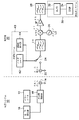
図1は、本発明による受信器の初期校正するための校正システム及び受信器のブロック図である。校正システム10は、後述の如く、パワー・メータ12、テスト・ポート14、信号発生器16及び方向性結合器18を具えている。また、受信器20は、後述の如く、入力ポート22、リレー24、正規化信号源(ソース)40、フィルタ25、局部発振器(LO)26、ミキサ27、中間周波数(IF)増幅器29、IFフィルタ28、取込みシステム30を具えている。正規化ソース40は、ノイズ信号源(ソース)42及び疑似ランダム・シーケンス(PRS)発生器44を具えており、取込みシステム30は、アナログ・デジタル(A/D)変換器32及びデジタル信号プロセッサ(DSP)34を具えている。局部発振器26、ミキサ27、IF増幅器29及びIFフィルタ28は、フィルタ25の出力信号と局部発振器26の出力信号との周波数差の信号を発生する中間周波数段を構成する。
【0011】
校正手順の第1ステップは、テスト・ポート14にてパワー・メータにより校正システム10を校正して、信号発生器16からのテスト・ポート14におけるパワーを求める。この代わりに、方向性結合器18をテスト・ポート14及び信号発生器16の間に設けて、方向性結合器18の結合ポートにて、他のパワー・メータ12によりパワーを測定するようにしてもよい。この際、このテスト・ポート14におけるパワーを用いて、振幅変化に対して校正システムをモニタする。このモニタが可能なのは、方向性結合器18の結合ポートがテスト・ポート14の負荷インピーダンスに反応しにくいためである。次に、入力ポート22を介して、被校正ブロードバンド受信器20をテスト・ポート14に結合し、リレー24を第1位置にして、受信器20を入力ポート22に結合する。電子的なRF(無線周波数)スイッチは、スイッチの温度ドリフトの影響を受けるので、リレー24は、好ましくは、温度安定性のよい機械式リレーである。校正システム10からの校正信号を入力ポート22に供給するが、受信器20の特定入力帯域幅にわたって周波数がステップ状に増分する一方、受信器20の局部発振器26もステップ状に同じに増分するので、校正信号は、IFフィルタ28のIF帯域幅の中央になる。取込みシステム30は、利得に対する周波数(利得対周波数)を表すテーブル(表)を求める。なお、上述のように、この取込みシステム30は、A/D変換器32及びデジタル信号プロセッサ34を含んでいる。次に、受信器のリレー24が入力ポート22から正規化ソース(信号源)40に切り替わり、ノイズ・ソース42がオン(動作状態)になる。このノイズ・レベルを同じ周波数増分にて測定し、取込みシステム30がノイズ・レベルに対する周波数(ノイズ・レベル対周波数)を表す表(ノイズ・レベル・テーブル)を求める。このノイズ・レベル・テーブルを校正と同じ時点及び温度で作成するので、このテーブルを温度安定基準のソース(よりどころ)として用いて、校正後の受信器利得の任意の変動を判断する。
【0012】
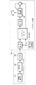
図2は、本発明によるIFバンド受信器の振幅/位相校正処理を行う機能ブロック図であり、図1の構成を基にして、原理的に必要なブロックのみを示している。なお、デジタル信号プロセッサ(DSP)34の内部機能もブロックとして示してある。また、図2の受信器20は、主に中間周波数段の機能を表している。上述の次のステップは、ノイズ信号源42をオフにし、疑似ランダム・シーケンス(PRS)発生器44をオンにして、受信器20を最低入力周波数に同調させる。疑似ランダム・シーケンス(PRS)波形を用い、データ補助適合等化技術(data-aided adaptive equalization technique)に基づいて、IF群遅延(位相)及び振幅変動をイコライズ(等化)、即ち、正規化する。正規化ソース40内のPRS発生器44からのPRSは、受信器20を介して、取込みシステム30(A/D変換器32及びDSP34)により取り込まれ、DSP34により更に処理される。なお、ブロック34は、DSP内部のソフトウェア処理を表す。PRSは、相関関係により、基準発生器からの基準信号に時間的に同期させられる。次に、基準信号のスペクトル内容とPRSとを位置合わせ(アラインメント)して、関心のある同じスペクトル帯域を抽出する。IFは、受信器20の総ての入力周波数に対して同じであるので、この抽出は、単一周波数にて行う必要がある。受信器20の入力周波数レンジが充分に低く、PRSのクロック・レートが充分に高ければ、ベースバンドのPRSには、受信器20の最低周波数でも、イコライズを行うのに充分なスペクトル内容がある。最低周波数に同調させる理由は、PRSが(sin x)/xのスペクトルを発生し、PRSのクロック周波数に第1ヌル点が存在するためである。正規化を行うのに充分なスペクトル内容を有するために、受信器20を第1ヌル点より下に同調させる必要がある。スペクトル合わせをして求めたデータは、平均化される。PRSに広いスペクトル内容が必要な場合、その波形は、スペクトルを広くする形状のパルスでもよい。この場合、矩形波PRSは、狭いパルスに整形してもよい。他の方法では、PRSをアップ・コンバートする。
【0013】
上述のこれらステップを実行すると、DSP34内の受信器ファームウェア(ソフトウェア)は、求めたテーブルを用いて、各周波数増分でのブロードバンド利得差(振幅)を補正して、IFを中心にする。この際、平均化したデータを用いて、適応等価器によって、疑似ランダム・シーケンスに対する等価フィルタ係数を求める。この際、適応等価器及びスペクトル合わせの出力データを組合せて、適応等価器を制御する。求めたフィルタ係数を用いる等化フィルタにより、IFを中心にして、IF帯域幅(位相)を補正する。正規化ソース40が温度(熱)に対して安定なので、これらソースを任意の時点で受信器20により切り替えて測定し、温度状態の変化によるブロードバンド受信器利得の校正後の変化や、IF線形歪の変化を正規化する。
【0014】
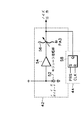
正規化ソース40の詳細なブロック図を図3に示す。ノイズ・ソース42は、+12ボルト及び接地の如き1対の電圧源の間に結合されたノイズ・ダイオード52を有する。ノイズ・ダイオード52の出力信号をモジューラ増幅器54に供給する。ノイズ・ダイオード52は、温度上昇により振幅が増加するが、モジューラ増幅器54は、小さな範囲で温度上昇により振幅が減少するので、全体としては、振幅がわずかに増加する。したがって、モジューラ増幅器54からの出力信号は、固定熱減衰器(熱PAD)56を介して、受信器リレー24に供給されるが、熱減衰器56により、上述の残った振幅増加(ノイズ・ダイオード52及びモジューラ増幅器54によるわずかな振幅増加)を補償する。熱減衰器56は、温度上昇により減衰が増加する。その結果により、全体的な振幅変化は、非常に小さく、摂氏10度から60度の温度変動に対して約0.1dBのオーダである。温度に対して、ノイズ・ダイオード52のパワー変動及びモジューラ増幅器54の利得変動を補償するように、減衰器56の熱係数が経験的に求まる。この補償は、熱減衰器56の代わりにDSP34によって行ってもよい。また、温度係数の高い減衰器56を用いることにより、モジューラ増幅器54を用いないで、温度安定化を達成することもできる。
【0015】
PRS発生器44にて疑似ランダム・シーケンス(PRS)を発生するのにプログラマブル・ロジック・アレイ(PLD)(図示せず)を用い、ECLに変換して、理想に近いPRS波形を発生できる。この場合、ECL出力フリップ・フロップ58により、このPRSを65MHzの如き高周波数でクロックして、即ち、PRSをフリップ・フロップ58のセット端子Sに供給すると共に、クロック(CLK)をフリップ・フロップ58のリセット端子Rに供給し、その出力端子Qからの出力信号を受信器リレー24に供給する。なお、このQ出力信号は、熱減衰器56を介して減衰されるようにしてもよい。受信器の最低入力周波数が30MHzならば、受信器がこの最低入力周波数に同調された場合、PRSは、1つのIFチャネル帯域幅にわたり意味のあるスペクトル内容を有する。これにより、PRSを、アップコンバートではなくベースバンドで使用できる。簡略化とは別に、この利点は、温度(熱)に対するECL出力の固有の波形安定性である。PRSをアップコンバートする必要があると、必要とされる混合処理や、フィルタ処理により、温度変化に応じて波形を歪ませたり、波形を変化させるかもしれない。パルス整形を用いた場合には、狭いパルスの幅を温度に対して安定化させるのが困難であり、わずかな変化でさえ、スペクトルに大きな変化が生じてしまう。よって、本発明の温度に対する安定性は、重要である。
【0016】
上述の如く、本発明によるブロードバンド受信器の振幅/位相の正規化では、ノイズ・ソース及びPRS発生器を含む内部の熱的に安定した正規化ソース(信号源)を用い、受信器が、外部の校正ソース(信号源)からの利得対周波数テーブルを求め、内部のノイズ・ソースに応じてノイズ・レベル対周波数テーブルを求め、PRS発生器に応じてIF等化フィルタの係数を求める。
【0017】
【発明の効果】
したがって、本発明によれば、温度に対して安定して状態で、振幅/位相を正規化できる。
【図面の簡単な説明】
【図1】本発明により受信器を初期校正するための校正システム及び受信器のブロック図である。
【図2】本発明によるIFバンド受信器の振幅/位相校正処理を行うブロック図である。
【図3】本発明による正規化信号源のブロック図である。
【符号の説明】
10 校正システム
12 パワー・メータ
14 テスト・ポート
16 信号発生器
18 方向性結合器
20 受信器
22 入力ポート
24 受信器リレー
26 局部発振器
28 中間周波数フィルタ
30 取込みシステム
32 アナログ・デジタル変換器
34 デジタル信号プロセッサ
40 正規化ソース
42 ノイズ信号源(ソース)
44 疑似ランダム・シーケンス発生器
52 ノイズ・ダイオード
54 モジューラ増幅器
56 熱減衰器[0001]
BACKGROUND OF THE INVENTION
The present invention relates generally to broadband receivers, and more particularly, to a broadband receiver that performs amplitude / phase normalization using a broadband temperature (thermal) compensated noise signal source and a pseudo-random sequence generator. It is related with the test equipment which has.
[0002]
[Prior art]
The gain of a broadband receiver is not constant over its input frequency range. However, a receiver provided in a test apparatus such as a spectrum analyzer needs to have a constant gain in order to accurately measure the amplitude of the input signal. To satisfy this need, amplitude calibration is typically performed, but a known level of input signal from the calibration signal generator is stepped over its input bandwidth. In this amplitude calibration, the gain difference with respect to frequency is recorded and the firmware of the test equipment uses this gain difference to ensure that the amplitude response of the receiver is correct.
[0003]
Broadband receivers mainly have group delay (phase variation) and amplitude variation over the signal channel bandwidth, mainly due to the narrowband filter required for the intermediate frequency (IF) stage of the receiver. In a receiver that digitizes and processes the output signal of the final IF stage, to equalize, ie normalize, the IF stage amplitude and frequency response, a known pseudo-random sequence is injected and the digital signal The process correlates these amplitude and frequency (phase) responses.
[0004]
[Problems to be solved by the invention]
One problem in these calibration steps is that the overall receiver gain (amplitude) and IF filter response (phase) vary with the post-calibration temperature (heat). This invalidates the calibration already performed.
[0005]
A broadband receiver can be readily used to normalize amplitude / phase as needed, but a temperature-stable, self-contained (independent) calibration system is desired.
[0006]
Accordingly, the present invention provides a test instrument comprising a receiver capable of normalizing amplitude / phase in a stable state with respect to temperature (heat), a heat-compensated noise signal source used in the test instrument, and amplitude / phase normalization. It provides a method.
[0007]
[Means for Solving the Problems]
The present invention comprises a broadband receiver (20) that includes a serially coupled input port (22), an intermediate frequency stage (26, 27, 29, 28) and a digital signal processor (34) for normalizing amplitude / phase. A test signal comprising: a normalized signal source (40) having an output; a first input coupled to the input port (22); a first coupled to the output of the normalized signal source (40); 2 inputs, and an intermediate frequency stage has a relay output coupled to the input terminal, the first input end at the first position is coupled to the output relay, the second input end at the second position There comprising a relay which is coupled to the output relay (24); a digital signal processor (34), when the relay is supplied calibrated test signal to the input port of the first position, the gain versus frequency relationship When the relay is in the second position , Have a generating means for generating a compensation data in accordance with the normalized signal source; normalized signal source has an output terminal coupled to the output of the normalized signal source, when coupled to an intermediate frequency stage by a relay A thermal compensation noise signal source (42) which causes the generating means to generate compensation data indicating the relationship between noise level and frequency, and the clock frequency is considerably higher than the lowest input frequency of the broadband receiver and is coupled to the intermediate frequency stage by a relay when it is, it is characterized in that chromatic pseudo random sequence generator for generating a normalized filter coefficients to compensate for the intermediate frequency data generating means (44).
Also, the present invention is series coupled input port (22), normalizes the amplitude / phase of the intermediate frequency stage (26,27,29,28)) and broadband receiver including a processor (34) (20) Supplying a calibrated signal (10 output signals) to the input port; determining a gain to frequency relationship for the calibrated signal with a processor; thermally compensated noise signal (42 outputs) Signal) to the intermediate frequency stage; the processor determines the noise level versus frequency relationship for the thermally compensated noise signal; and supplies a pseudo-random sequence (44 output signals) to the intermediate frequency stage at baseband And an equivalent filter coefficient for the pseudo-random sequence is obtained by a processor.
[0008]
Amplitude / phase normalization in a broadband receiver according to the present invention uses a broadband temperature compensated noise signal source and a pseudo-random sequence (PRS) generator. The broadband receiver includes a noise signal source and a PRS generator, which are normalized signal sources that internally compensate for temperature. The receiver relay supplies a signal from an input port or normalized signal source to the receiver. At the first position of the relay, the calibration signal source supplies calibration signals to the receiver at stepped frequency intervals and generates a table showing the relationship of frequency to gain (gain vs. frequency). In addition, the internal noise signal source is switched at the same stepped frequency interval to obtain a table indicating the relationship of the frequency to the noise level. Next, the filter coefficient for the IF equalization filter is obtained by switching the PRS generator at the lowest input frequency to the receiver. Normalized signal sources are stable over temperature (heat), so switch between these sources at any point in time and measure any subsequent broadband receiver gain changes or IF linear distortions due to temperature state changes. Normalize changes in.
[0009]
Objects, advantages and novel features of the invention will become apparent from the following detailed description when taken in conjunction with the accompanying drawings.
[0010]
DETAILED DESCRIPTION OF THE INVENTION
FIG. 1 is a block diagram of a calibration system and receiver for initial calibration of a receiver according to the present invention. The
[0011]
The first step in the calibration procedure is to calibrate the
[0012]
FIG. 2 is a functional block diagram for performing amplitude / phase calibration processing of the IF band receiver according to the present invention, and shows only the blocks that are necessary in principle based on the configuration of FIG. The internal function of the digital signal processor (DSP) 34 is also shown as a block. 2 mainly represents the function of the intermediate frequency stage. The next step described above turns off the
[0013]
After performing these steps described above, the receiver firmware (software) in the
[0014]
A detailed block diagram of the
[0015]
A
[0016]
As described above, the amplitude / phase normalization of the broadband receiver according to the present invention uses an internal thermally stable normalization source (signal source) including a noise source and a PRS generator, and the receiver is externally connected. The gain vs. frequency table from the calibration source (signal source) is obtained, the noise level vs. frequency table is obtained according to the internal noise source, and the IF equalization filter coefficient is obtained according to the PRS generator.
[0017]
【The invention's effect】
Therefore, according to the present invention, the amplitude / phase can be normalized in a stable state with respect to temperature.
[Brief description of the drawings]
FIG. 1 is a block diagram of a calibration system and receiver for initial calibration of a receiver according to the present invention.
FIG. 2 is a block diagram for performing amplitude / phase calibration processing of an IF band receiver according to the present invention;
FIG. 3 is a block diagram of a normalized signal source according to the present invention.
[Explanation of symbols]
10
44
Claims (2)
出力端を有する正規化信号源と、
上記入力ポートに結合された第1入力端、上記正規化信号源の出力端に結合された第2入力端、及び上記中間周波数段の入力端に結合されたリレー用出力端を有し、第1位置にて上記第1入力端が上記リレー用出力端に結合され、第2位置にて上記第2入力端が上記リレー用出力端に結合されたリレーとを具え、
上記デジタル信号プロセッサは、上記入力ポートに校正されたテスト信号が供給され上記リレーが上記第1位置のときに、利得対周波数の関係を求め、上記リレーが上記第2位置のときに、上記正規化信号源に応じて補償データを発生する発生手段を有し、
上記正規化信号源は、
出力端が上記正規化信号源の出力端に結合され、上記リレーにより上記中間周波数段に結合されたときに、ノイズ・レベル対周波数の関係を示す補償データを上記発生手段に発生させる熱補償ノイズ信号源と、
クロック周波数が上記ブロードバンド受信器の最低入力周波数よりもかなり高く、上記リレーにより上記中間周波数段に結合されたときに、中間周波数データを補償する正規化フィルタ係数を上記発生手段に発生させる疑似ランダム・シーケンス発生器とを有することを特徴とするテスト機器。A test instrument comprising a broadband receiver that includes a serially coupled input port, an intermediate frequency stage and a digital signal processor and normalizes amplitude / phase,
A normalized signal source having an output; and
A first input coupled to the input port; a second input coupled to the output of the normalized signal source; and a relay output coupled to the input of the intermediate frequency stage; 1 position the first input coupled to the output terminal for the relays in the above second input terminal comprises a relay which is coupled to the output terminal for the relay at the second position,
The digital signal processor determines a gain vs. frequency relationship when a calibrated test signal is supplied to the input port and the relay is in the first position, and the normal signal is obtained when the relay is in the second position. have a generating means for generating a compensation data in accordance with a signal source,
The normalized signal source is
Thermal compensation noise that causes the generating means to generate compensation data indicating the relationship between noise level and frequency when the output terminal is coupled to the output terminal of the normalized signal source and coupled to the intermediate frequency stage by the relay. A signal source;
A pseudo-random random number that causes the generating means to generate normalized filter coefficients that compensate for intermediate frequency data when the clock frequency is significantly higher than the lowest input frequency of the broadband receiver and coupled to the intermediate frequency stage by the relay. test equipment characterized by chromatic and sequence generator.
上記入力ポートに校正された信号を供給し、
上記校正された信号に対する利得対周波数の関係を上記プロセッサで求め、
熱的に補償されたノイズ信号を上記中間周波数段に供給し、
上記熱的に補償されたノイズ信号に対するノイズ・レベル対周波数の関係を上記プロセッサで求め、
疑似ランダム・シーケンスをベースバンドで上記中間周波数段に供給し、
上記疑似ランダム・シーケンスに対する等価フィルタ係数を上記プロセッサで求める
ことを特徴とするブロードバンド受信器の振幅/位相の正規化方法。A method for normalizing the amplitude / phase of a broadband receiver comprising a serially coupled input port, an intermediate frequency stage and a processor comprising:
Supply the calibrated signal to the above input port,
Determining the gain versus frequency relationship for the calibrated signal with the processor;
Supplying a thermally compensated noise signal to the intermediate frequency stage;
Determining the noise level versus frequency relationship for the thermally compensated noise signal with the processor;
Supply a pseudo-random sequence in baseband to the intermediate frequency stage,
A method for normalizing amplitude / phase of a broadband receiver, wherein the processor obtains an equivalent filter coefficient for the pseudo-random sequence.
Applications Claiming Priority (2)
| Application Number | Priority Date | Filing Date | Title |
|---|---|---|---|
| US09/660,561 | 2000-09-12 | ||
| US09/660,561 US6636722B1 (en) | 2000-09-12 | 2000-09-12 | Broadband receiver amplitude/phase normalization using a broadband temperature compensated noise source and a pseudo random sequence generator |
Publications (2)
| Publication Number | Publication Date |
|---|---|
| JP2002190781A JP2002190781A (en) | 2002-07-05 |
| JP3973386B2 true JP3973386B2 (en) | 2007-09-12 |
Family
ID=24650023
Family Applications (1)
| Application Number | Title | Priority Date | Filing Date |
|---|---|---|---|
| JP2001272168A Expired - Fee Related JP3973386B2 (en) | 2000-09-12 | 2001-09-07 | Test equipment |
Country Status (4)
| Country | Link |
|---|---|
| US (1) | US6636722B1 (en) |
| EP (1) | EP1187376B1 (en) |
| JP (1) | JP3973386B2 (en) |
| DE (1) | DE60124358T2 (en) |
Families Citing this family (18)
| Publication number | Priority date | Publication date | Assignee | Title |
|---|---|---|---|---|
| US6842608B2 (en) * | 2001-10-10 | 2005-01-11 | Agilent Technologies, Inc. | Response calibration scheme using frequency-shifted stimulus signals |
| US6940922B2 (en) * | 2001-10-10 | 2005-09-06 | Agilent Technologies, Inc. | Response calibration method using a frequency-shifted receiver |
| FI20012108L (en) * | 2001-10-31 | 2003-05-01 | Elektrobit Oy | Method and apparatus for simulating a radio channel |
| US7310504B2 (en) * | 2004-03-26 | 2007-12-18 | Agilent Technologies, Inc. | IF frequency response characterization employing overlapping frequency bands |
| US20050260963A1 (en) * | 2004-05-19 | 2005-11-24 | Motorola, Inc. | Receiver system and method for wideband self test |
| US7453934B2 (en) * | 2005-06-27 | 2008-11-18 | Nokia Corporation | Automatic receiver calibration with noise and fast fourier transform |
| US7649930B2 (en) * | 2005-11-09 | 2010-01-19 | Tektronix, Inc. | Filter equalization using magnitude measurement data |
| US8055226B2 (en) * | 2006-10-18 | 2011-11-08 | Tektronix, Inc. | Frequency response correction for a receiver having a frequency translation device |
| DE102007007357B4 (en) | 2007-02-14 | 2018-06-21 | Infineon Technologies Ag | Integrated circuit arrangement |
| JP4704384B2 (en) * | 2007-03-20 | 2011-06-15 | アンリツ株式会社 | Spectrum analyzer |
| US8880063B2 (en) * | 2009-02-23 | 2014-11-04 | Mediatek Inc. | Method and user equipment with dual RF transceivers to perform PLMN list generation or PLMN search |
| US7945822B1 (en) * | 2009-04-27 | 2011-05-17 | Netapp, Inc. | Storing data to multi-chip low-latency random read memory device using non-aligned striping |
| US8599050B2 (en) * | 2012-01-06 | 2013-12-03 | Maxlinear, Inc. | Method and system for broadband analog to digital converter technology |
| JP2017055261A (en) * | 2015-09-09 | 2017-03-16 | 株式会社東芝 | Quadrature demodulator and radio receiver |
| JP6867346B2 (en) * | 2017-10-13 | 2021-04-28 | アンリツ株式会社 | Antenna device and measurement method |
| CN109842379B (en) * | 2017-11-29 | 2023-09-19 | 北京振兴计量测试研究所 | A broadband noise generation method |
| GB2620734A (en) * | 2022-07-14 | 2024-01-24 | Cambridge Entpr Ltd | A physical random variate generator |
| CN116299124B (en) * | 2023-03-22 | 2025-09-30 | 电子科技大学 | A fast temperature compensation method for oscilloscope amplitude calibration |
Family Cites Families (28)
| Publication number | Priority date | Publication date | Assignee | Title |
|---|---|---|---|---|
| FR1520380A (en) * | 1965-03-02 | 1968-04-12 | Electronic component with incorporated thermal regulation | |
| US3675148A (en) * | 1969-06-06 | 1972-07-04 | Solitron Devices | Random noise generator diode with impedance matched transistor amplifier |
| US3731186A (en) * | 1971-06-01 | 1973-05-01 | H Sadel | Radio frequency measurements |
| US4031469A (en) | 1975-09-10 | 1977-06-21 | The Singer Company | Receiver gain calibration |
| DE2803480C2 (en) * | 1978-01-27 | 1984-11-22 | Philips Patentverwaltung Gmbh, 2000 Hamburg | Method and arrangement for measuring the physical object temperature by means of microwaves |
| US4185251A (en) | 1978-06-05 | 1980-01-22 | Raytheon Company | Compensated automatic gain control |
| EP0064198B1 (en) * | 1981-04-25 | 1985-12-18 | Kabushiki Kaisha Toshiba | Apparatus for measuring noise factor and available gain |
| US4685065A (en) | 1985-05-23 | 1987-08-04 | Comsonics, Inc. | Portable sampling spectrum analyzer |
| US4740996A (en) | 1986-11-17 | 1988-04-26 | Amp Incorporated | Temperature independent, low level, AM modem receiver |
| US4849710A (en) | 1988-04-27 | 1989-07-18 | Litton Systems, Inc. | Temperature compensated high gain FET amplifier |
| CA2030272C (en) | 1989-11-24 | 1995-06-27 | David R. Brunfeldt | Vector network analyzer |
| TW258797B (en) | 1990-08-24 | 1995-10-01 | Sony Co Ltd | |
| US5162678A (en) | 1990-09-18 | 1992-11-10 | Silicon Systems, Inc. | Temperature compensation control circuit for exponential gain function of an agc amplifier |
| US5262957A (en) | 1990-11-09 | 1993-11-16 | Global Communications, Inc. | Inexpensive portable RF spectrum analyzer with calibration features |
| DE69021574T2 (en) | 1990-12-12 | 1996-02-01 | Sgs Thomson Microelectronics | Integrated circuit for generating a temperature-independent current, which is proportional to the voltage difference between a signal and a reference voltage. |
| FI90383C (en) | 1992-03-09 | 1994-01-25 | Nokia Mobile Phones Ltd | Method for stabilizing the reference frequency in a radio telephone |
| JP2948054B2 (en) | 1993-05-21 | 1999-09-13 | アルプス電気株式会社 | Transceiver |
| US5339046A (en) | 1993-06-03 | 1994-08-16 | Alps Electric Co., Ltd. | Temperature compensated variable gain amplifier |
| US5408697A (en) | 1993-06-14 | 1995-04-18 | Qualcomm Incorporated | Temperature-compensated gain-controlled amplifier having a wide linear dynamic range |
| CA2145697A1 (en) | 1994-04-15 | 1995-10-16 | Michael F. Mattes | Method and apparatus for compensating for temperature fluctuations in the input to a gain circuit |
| GB9418754D0 (en) * | 1994-09-16 | 1994-11-02 | Ionica L3 Limited | Telecommunications receiver |
| US5481186A (en) * | 1994-10-03 | 1996-01-02 | At&T Corp. | Method and apparatus for integrated testing of a system containing digital and radio frequency circuits |
| US5688050A (en) | 1995-04-03 | 1997-11-18 | Mmtc, Inc. | Temperature-measuring microwave radiometer apparatus |
| US5881376A (en) | 1995-12-15 | 1999-03-09 | Telefonaktiebolaget Lm Ericsson | Digital calibration of a transceiver |
| US5913158A (en) | 1997-01-17 | 1999-06-15 | Sullivan; William B. | Dynamic temperature measurement |
| CN1108037C (en) * | 1997-03-18 | 2003-05-07 | 松下电器产业株式会社 | Cablibration device for array antenna wireless receiver |
| US6268735B1 (en) * | 1999-06-04 | 2001-07-31 | Teradyne, Inc. | Noise source module for microwave test systems |
| US6297709B1 (en) * | 1999-07-14 | 2001-10-02 | Nokia Telecommunications Oy | Temperature compensated variable attenuator |
-
2000
- 2000-09-12 US US09/660,561 patent/US6636722B1/en not_active Expired - Fee Related
-
2001
- 2001-09-04 DE DE60124358T patent/DE60124358T2/en not_active Expired - Lifetime
- 2001-09-04 EP EP01307517A patent/EP1187376B1/en not_active Expired - Lifetime
- 2001-09-07 JP JP2001272168A patent/JP3973386B2/en not_active Expired - Fee Related
Also Published As
| Publication number | Publication date |
|---|---|
| EP1187376A3 (en) | 2004-07-28 |
| JP2002190781A (en) | 2002-07-05 |
| DE60124358T2 (en) | 2007-10-11 |
| US6636722B1 (en) | 2003-10-21 |
| EP1187376A2 (en) | 2002-03-13 |
| EP1187376B1 (en) | 2006-11-08 |
| DE60124358D1 (en) | 2006-12-21 |
Similar Documents
| Publication | Publication Date | Title |
|---|---|---|
| JP3973386B2 (en) | Test equipment | |
| CN100459441C (en) | Transmitter and transmission method | |
| KR101564280B1 (en) | Transmit power calibration in a communication system | |
| US5059892A (en) | Radio frequency signal interface | |
| CA2357491A1 (en) | Filter tuning using direct digital sub-sampling | |
| TW200713855A (en) | In-situ gain calibration of radio frequency devices using thermal noise | |
| US8200174B2 (en) | Systems and methods for controlling a transmitter | |
| US20120258675A1 (en) | Antenna Tuner in Combination with Modified Feedback Receiver for Improved Antenna Matching | |
| Verspecht et al. | The vector component analyzer: A new way to characterize distortions of modulated signals in high-frequency active devices | |
| JP2018074587A (en) | Noise filter and method of using noise filter | |
| Dao et al. | I/Q imbalance calibration method for 5G ultra-wideband transceivers | |
| JP2002158546A (en) | System and method for producing signal amplified using plural amplitudes across spectrum | |
| Rotbøll et al. | A novel L‐band polarimetric radiometer featuring subharmonic sampling | |
| TW202010246A (en) | Transmitter circuit capable of measuring transmitter-side image rejection ratio | |
| KR101184331B1 (en) | Apparatus and method for detecting passive intermodulation distortion signal | |
| Laemmle et al. | A 62 GHz reflectometer for biomedical sensor readout in SiGe BiCMOS technology | |
| US20060223440A1 (en) | Low frequency noise source and method of calibration thereof | |
| Schoch et al. | Wideband cross-domain characterization of a W-band amplifier MMIC | |
| US6456092B1 (en) | Network vector channel analyzer | |
| WO2012011141A1 (en) | Process for automatically calibrating wideband microwave modules" | |
| US7515662B2 (en) | Method for compensating for gain ripple and group delay characteristics of filter and receiving circuit embodying the same | |
| JPH01209395A (en) | Pulse compression radar | |
| Zhang et al. | Repeatable phase spectrum measurements of 75–110-GHz modulated signals using a VNA-based LO phase cancellation technique | |
| Wang et al. | Considerations for measurement setup for second-order nonlinearity in radio-frequency bulk acoustic wave duplexers | |
| Brown et al. | Far field EVM characterization of antenna frequency response via full-wave analysis |
Legal Events
| Date | Code | Title | Description |
|---|---|---|---|
| A625 | Written request for application examination (by other person) |
Free format text: JAPANESE INTERMEDIATE CODE: A625 Effective date: 20040702 |
|
| RD04 | Notification of resignation of power of attorney |
Free format text: JAPANESE INTERMEDIATE CODE: A7424 Effective date: 20060602 |
|
| A977 | Report on retrieval |
Free format text: JAPANESE INTERMEDIATE CODE: A971007 Effective date: 20061018 |
|
| A131 | Notification of reasons for refusal |
Free format text: JAPANESE INTERMEDIATE CODE: A131 Effective date: 20061031 |
|
| A601 | Written request for extension of time |
Free format text: JAPANESE INTERMEDIATE CODE: A601 Effective date: 20070117 |
|
| A602 | Written permission of extension of time |
Free format text: JAPANESE INTERMEDIATE CODE: A602 Effective date: 20070122 |
|
| A521 | Request for written amendment filed |
Free format text: JAPANESE INTERMEDIATE CODE: A523 Effective date: 20070418 |
|
| TRDD | Decision of grant or rejection written | ||
| A01 | Written decision to grant a patent or to grant a registration (utility model) |
Free format text: JAPANESE INTERMEDIATE CODE: A01 Effective date: 20070605 |
|
| A61 | First payment of annual fees (during grant procedure) |
Free format text: JAPANESE INTERMEDIATE CODE: A61 Effective date: 20070612 |
|
| R150 | Certificate of patent or registration of utility model |
Free format text: JAPANESE INTERMEDIATE CODE: R150 |
|
| FPAY | Renewal fee payment (event date is renewal date of database) |
Free format text: PAYMENT UNTIL: 20100622 Year of fee payment: 3 |
|
| FPAY | Renewal fee payment (event date is renewal date of database) |
Free format text: PAYMENT UNTIL: 20110622 Year of fee payment: 4 |
|
| FPAY | Renewal fee payment (event date is renewal date of database) |
Free format text: PAYMENT UNTIL: 20110622 Year of fee payment: 4 |
|
| FPAY | Renewal fee payment (event date is renewal date of database) |
Free format text: PAYMENT UNTIL: 20120622 Year of fee payment: 5 |
|
| FPAY | Renewal fee payment (event date is renewal date of database) |
Free format text: PAYMENT UNTIL: 20120622 Year of fee payment: 5 |
|
| FPAY | Renewal fee payment (event date is renewal date of database) |
Free format text: PAYMENT UNTIL: 20130622 Year of fee payment: 6 |
|
| LAPS | Cancellation because of no payment of annual fees |