JP3937649B2 - Developing device and process cartridge - Google Patents
Developing device and process cartridge Download PDFInfo
- Publication number
- JP3937649B2 JP3937649B2 JP12364699A JP12364699A JP3937649B2 JP 3937649 B2 JP3937649 B2 JP 3937649B2 JP 12364699 A JP12364699 A JP 12364699A JP 12364699 A JP12364699 A JP 12364699A JP 3937649 B2 JP3937649 B2 JP 3937649B2
- Authority
- JP
- Japan
- Prior art keywords
- contact
- developing roller
- developing
- magnet
- conductive portion
- Prior art date
- Legal status (The legal status is an assumption and is not a legal conclusion. Google has not performed a legal analysis and makes no representation as to the accuracy of the status listed.)
- Expired - Fee Related
Links
Images


Landscapes
- Magnetic Brush Developing In Electrophotography (AREA)
- Developing For Electrophotography (AREA)
- Dry Development In Electrophotography (AREA)
Description
【0001】
【発明の属する技術分野】
本発明は、電子写真画像形成装置に用いられる現像装置、およびプロセスカートリッジに関するものである。
【0002】
ここで、電子写真画像形成装置とは、電子写真画像形成方式を用いて記録媒体に画像を形成するものである。そして、電子写真画像形成装置の例としては、例えば、電子写真複写機、電子写真プリンタ(例えば、レーザービームプリンタ、LEDプリンタ等)、ファクシミリ装置及びワードプロセッサ等が含まれる。
【0003】
また、プロセスカートリッジとは、帯電手段、現像手段またはクリーニング手段と電子写真感光体ドラムとを一体的にカートリッジ化し、このカートリッジを電子写真画像形成装置本体に対して着脱可能とするものである。及び帯電手段、現像手段、クリーニング手段の少なくとも1つと電子写真感光体ドラムとを一体的にカートリッジ化して電子写真画像形成装置本体に着脱可能とするものである。更に、少なくと現像手段と電子写真感光体ドラムとを一体的にカートリッジ化して電子写真画像形成装置本体に着脱可能とするものをいう。
【0004】
【従来の技術】
従来、電子写真画像形成プロセスを用いた電子写真画像形成装置においては、電子写真感光体ドラム及び前記電子写真感光体ドラムに作用するプロセス手段を一体的にカートリッジ化して、このカートリッジを電子写真画像形成装置本体に着脱可能とするプロセスカートリッジ方式が採用されている。このプロセスカートリッジ方式によれば、電子写真画像形成装置のメンテナンスをサービスマンによらずにユーザー自身で行うことができるので、格段に操作性を向上させることができた。そこで、このプロセスカートリッジ方式は、画像形成装置において広く用いられている。
【0005】
このようなプロセスカートリッジでは、電子写真感光体に形成された静電潜像を現像するための現像装置としての現像手段を有し、トナー(現像剤)を用いて、電子写真感光体に形成された静電潜像を現像ローラにより現像している。すなわち、現像ローラに現像バイアスを印加して現像ローラ上のトナーを静電潜像に応じて電子写真感光体に移転させることによってトナー像(現像剤像)を形成して可視像化している。
【0006】
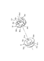
現像ローラに現像バイアスを印加する方法としては、図10に示すように、現像ローラDの端部に導電性部材よりなるフランジ部材Fを設け、前記フランジ部材Fには圧縮コイルバネSpよりなる電極を電気的に導通可能に取り付け、前記圧縮コイルバネSpの一端側を現像装置のハウジングHに取り付けられた接点部材Cに接触させる。そして、現像装置を装置本体に装着した際に、装置本体に設けられた給電部材Vに前記接点部材Cを電気的に導通させて接触させる方法が提案されている。
【0007】
また、現像ローラに現像バイアスを印加する別の方法としては、図11に示すように、前記接点部材Cに弾性当接部Csを設け、前記現像ローラDの端部に設けた導電性部材よりなるフランジ部材Fに前記弾性当接部Csを当接させる。そして、現像装置を装置本体に装着した際に、装置本体に設けられた給電部材Vに前記接点部材Cを電気的に導通させて接触させる方法も提案されている。
【0008】
このような場合、圧縮コイルバネSp或いはフランジ部材Fは、現像ローラDと一体的に回転して、接点部材Cと摺動するので、その摺動部分Cpに導電性のグリスを塗布するのが一般的である。
【0009】
【発明が解決しようとする課題】
本発明は上記従来技術を更に発展させたものであり、その主要な目的は、現像ローラに現像バイアスを印加するための接点部の信頼性の向上を図ることのできる現像装置を提供することにある。
【0010】
他の主要な目的は、現像ローラに現像バイアスを印加するための接点部の信頼性の向上を図ることのできるプロセスカートリッジを提供することにある。
【0013】
【課題を解決するための手段】
本発明に係る現像装置の代表的な構成は、
電子写真画像形成装置に用いられる現像装置であって、電子写真感光体に形成された静電潜像を現像するための現像装置において、
フレームと、
前記フレームに設けられ、現像剤を用いて、前記電子写真感光体に形成された静電潜像を現像するための現像ローラと、
前記現像ローラの内部に設けられたマグネットと、
前記マグネットの一端に設けられ、円弧部分と平坦部分を有するDカット形状部であって、前記フレームに対する前記マグネットの位置を決めるために前記フレームに設けられた穴に嵌合しているDカット形状部と、
前記一端に取り付けられ、前記現像ローラと電気的に接続している第一の導電部であって、前記円弧部分上に位置する第一の導電部と、
前記フレームに設けられ、前記第一の導電部と電気的に接続するための第一の電気接点部と、前記現像装置が電子写真画像形成装置本体に装着された際に、前記電子写真画像形成装置本体に設けられた本体電気接点と接続するための第二の電気接点部と、を有する第三の導電部と、
を有し、
前記第一の導電部が前記第一の電気接点部と接触することにより付勢され、前記第一の導電部によって前記Dカット形状部が前記円弧部分から前記平坦部分の方向に向かって付勢されることを特徴とする現像装置である。
【0014】
本発明に係るプロセスカートリッジの代表的な構成は、
電子写真画像形成装置本体に着脱可能なプロセスカートリッジにおいて、
(a)電子写真感光体と、
(b)電子写真感光体に形成された静電潜像を現像する現像装置と、
を有し、
前記現像装置は、フレームと、前記フレームに設けられ、現像剤を用いて、前記電子写真感光体に形成された静電潜像を現像するための現像ローラと、前記現像ローラの内部に設けられたマグネットと、前記マグネットの一端に設けられ、円弧部分と平坦部分を有するDカット形状部であって、前記フレームに対する前記マグネットの位置を決めるために前記フレームに設けられた穴に嵌合しているDカット形状部と、前記一端に取り付けられ、前記現像ローラと電気的に接続している第一の導電部であって、前記円弧部分上に位置する第一の導電部と、前記フレームに設けられ、前記第一の導電部と電気的に接続するための第一の電気接点部と、前記現像装置が電子写真画像形成装置本体に装着された際に、前記電子写真画像形成装置本体に設けられた本体電気接点と接続するための第二の電気接点部と、を有する第三の導電部と、を有し、前記第一の導電部が前記第一の電気接点部と接触することにより付勢され、前記第一の導電部によって前記Dカット形状部が前記円弧部分から前記平坦部分の方向に向かって付勢されることを特徴とするプロセスカートリッジである。
【0023】
【発明の実施の形態】
以下、本発明に係る実施の形態を図面を用いて詳細に説明する。
【0024】
図1乃至図9に本実施形態に係る現像装置及び前記現像装置を有するプロセスカートリッジ及びこれを装着可能な電子写真画像形成装置を示す。
【0025】
ここでは説明の順序として、先ず図7乃至図9を参照してプロセスカートリッジ及びこれを用いる電子写真画像形成装置の全体構成を説明し、次に図1乃至図6を参照して現像ローラの接点構成について説明する。そして図14乃至図16を参照してその接点構成についての組立てミスを防止するための構成を説明する。
【0026】
{全体構成}
この電子写真画像形成装置(レーザービームプリンタ)Aは、図7に示すように、光学系1から画像情報に基づいた情報光をドラム形状の電子写真感光体(以下「感光体ドラム」という)7へ照射して該感光体ドラム7に静電潜像を形成し、この潜像をトナー(現像剤)を用いて現像してトナー像を形成する。そして前記トナー像の形成と同期して、記録紙、OHPシートなどの記録媒体2をカセット3aからピックアップローラ3bおよびこれに圧接した圧接部材3cで一枚ずつ分離給送すると共に、搬送ローラ対3d、レジストローラ対3e等からなる搬送手段3で搬送し、且つプロセスカートリッジBとしてカートリッジ化された前記感光体ドラム7に形成したトナー像を転写手段としての転写ローラ4に電圧印加することによって記録媒体2に転写し、その記録媒体2を搬送ベルト3fによって定着手段5へと搬送する。この定着手段5は駆動ローラ5aと、ヒータ5bを内蔵すると共に支持体5cで回転可能に支持された筒状シートからなる定着回転体5dとからなり、通過する記録媒体2に熱及び圧力を印加して転写トナー像を記録媒体2に定着する。そしてこの記録媒体2を排出ローラ対3g,3hで搬送し、反転搬送経路を通して排出部6へと排出する如く構成している。尚、この画像形成装置Aは、手差しトレイ3i及びローラ3jによって手差し給紙も可能となっている。
【0027】
{プロセスカートリッジの構成}
一方、前記プロセスカートリッジBは、電子写真感光体と、少なくとも1つのプロセス手段を備えたものである。ここでプロセス手段としては、例えば電子写真感光体を帯電させる帯電手段、電子写真感光体に形成された潜像を現像する現像手段、電子写真感光体表面に残留するトナーをクリーニングするためのクリーニング手段等がある。
【0028】
本実施の形態のプロセスカートリッジBは、図8に示すように、感光層を有する電子写真感光体である感光体ドラム7を回転し、帯電手段である帯電ローラ8へ電圧印加して前記感光体ドラム7の表面を一様に帯電し、この帯電した感光体ドラム7に対して前記光学系1からの光像を開口部9を介して露光して静電潜像を形成する。そして該潜像を現像装置である現像手段10によって現像するように構成している。
【0029】
前記現像手段10は、トナー収納部10a内のトナーを送り手段である回転可能な第1送り部材10b1及び第2送り部材10b2で送り出す。そして固定磁石(以下「磁石」という)10cを内蔵したトナー担持体である現像ローラ10dを回転させると共に、現像ブレード10eによって摩擦帯電電荷を付与したトナー層を現像ローラ10dの表面に形成し、現像バイアスを印加してトナーを前記潜像に応じて感光体ドラム7へ転移させることによってトナー像を形成して可視像化するものである。
【0030】
そして転写ローラ4に前記トナー像と逆極性の電圧を印加してトナー像を記録媒体2に転写した後は、クリーニングブレード11aによって感光体ドラム7に残留したトナーを掻き落とすと共に、スクイシート11bによってすくい取り、除去トナー収納部11cへ集めるクリーニング手段11によって感光体ドラム7上の残留トナーを除去するように構成している。
【0031】
本実施の形態で示すプロセスカートリッジBは、トナー収納部10aを有する現像枠体12aと現像下枠12b及び蓋部材12cを一体的に溶着した現像手段10のフレームとしてのトナー現像枠体12に現像ローラ10d、現像ブレード10e等の各部材を収納する。そして、このトナー現像枠体12と、感光体ドラム7、帯電ローラ8、クリーニング手段11等の各部材を収納したクリーニング枠体13とを結合してカートリッジ化され、装置本体14に設けたカートリッジ装着手段に対して着脱可能に装着される。
【0032】
プロセスカートリッジBの着脱は、図7に示すように、軸15aを中心にして開閉部材15を開いて行うものであり、前記開閉部材15を開くと装置本体14内にはカートリッジ装着スペースが設けてある。この装着スペースの左右両側のフレーム16には、図9に示すように、カートリッジ装着ガイド部材17が対向して取り付けてある(図9には一方側のみ図示)。一方、プロセスカートリッジBの長手方向両外側面にはボス(図8参照)が突出形成してあり、このボス18を前記左右のガイド部材17とフレーム16とによって形成されるガイド溝19に沿わせてプロセスカートリッジBを挿入する。前記溝19の奥部には凹部19aが形成してあり、この凹部19aに前記ボス18の軸部18aを落とし込んでプロセスカートリッジBを装着する。このとき、感光体ドラム7の長手方向端部に取り付けた不図示のドラムギアが装置本体14に設けてある駆動ギアと噛合して感光体ドラム7へ駆動伝達が行われるようになる。
【0033】
{現像ローラの接点構成}
次に前記現像ローラ10dに現像バイアスを印加するための接点構成について、図1から図6を参照して説明する。
【0034】
図1に示すように、現像ローラ10dはアルミニウム、ステンレス鋼等の導電性、非磁性の円筒状部材で構成され、その左右両端に嵌合固定させたフランジ部材20a,20bを備えている。右側のフランジ部材20aは、現像ローラ10dの右端部10dRに圧入、接着、カシメ等の方法によって固定されており、現像ローラ10dの長手方向に沿って右端部10dRから外側へ突き出た軸部20a1を有する。前記軸部20a1は、その外周がトナー現像枠体12とホルダー24aに固定された軸受21aによって回動自在に支持されている。
【0035】
一方、現像ローラ10dの左端部10dLにはアルミニウム、ステンレス鋼等の金属からなるフランジ部材20bが圧入、カシメ等の機械的方法によって固定されており、現像ローラ10dの長手方向に沿って左端部10dLから外側へ突き出たフランジとしての軸部20b1を有する。フランジとしての軸部20b1は、その外周がトナー現像枠体12とホルダー24bに固定された軸受21bによって回動自在に支持されている。そして、前記軸部20b1にはローラギア22がキー、セットスクリュー等の方法で固定されている。これにより、現像ローラ10dは感光体ドラム7に組付けられたドラムギア(不図示)からローラギア22へ駆動力が伝えられ、現像ローラ10dが所定の回転数で回転駆動される。
【0036】
なお、本実施形態によれば、フランジとしての軸部20b1をアルミニウム、ステンレス鋼等の金属とした。これによって、現像ローラ10dを支持する支持剛性が向上した。従って、現像ローラ10dの回転精度を向上させることができた。本実施形態においては、前記軸部20b1と後述する第一の導電部とは非接触である。従って、前記軸部20b1から現像ローラ10dへ現像バイアスが給電されることはない。
【0037】
また、前記現像ローラ10dには複数の極性を有する磁石10cが内包されている。磁石10cは左右両端に軸部10c1を有する。そして、この左右の軸部10c1はそれぞれフランジ部材20a,20bの中心孔20a2,20b2を突き抜け、トナー現像枠体12に固定されたホルダー24a,24bの支持穴24a1,24b1に固定支持されている。
【0038】
(第一の導電部(円筒電極及び固定接点)の構成)
図2及び図3に示すように、磁石10cの左側の一端に設けられた一端軸としての軸部(以下「左側軸部」という)10c1には導電性を有する円筒電極28と固定接点29が組付けられている。この円筒電極28及び固定接点29は何れも第一の導電部を構成する構成部品である。
【0039】
円筒電極28はトナー現像枠体12の長手方向(感光体ドラム7の軸線方向)に沿って磁石10cの左側軸部10c1に設けられる。前記円筒電極28は現像ローラ10dの軸線方向に伸びる円筒としての円筒部28eを中央に有し、この円筒部28eの左右両端に前記現像ローラ10dの軸線方向に伸びた突出部としての突起部28a,28bを有する。そして、円筒部28eには現像ローラ10dの軸線方向に沿ってスリット28cが形成されている。前記円筒部28eの内径は磁石10cの左側軸部10c1の外径よりわずかに小さくしてある。このため、円筒部28eを磁石10cの左側軸部10c1に嵌めると、円筒部28eが径方向に拡大して、スリット28cをわずかに拡げ、そのスリット28cを狭めようとする円筒部28eの左側軸部10c1への締め付け力によって円筒電極28が左側軸部10c1に固定される。
【0040】
磁石10cの左側軸部10c1の根本部分には、周方向に数箇所、左側軸部10c1の半径方向に突出して軸方向で先端側に伸びた凸部10c2(本実施形態では3箇所)を設け、先端部分には、磁石10cの磁極位置決めに用いる角度固定用のDカット10c3が設けてある。円筒電極28は、円筒部28eの左側軸部10c1に対する回転を規制するため、図2に示すように、円筒部28eの右端側に設けた複数の突起部28aがそれぞれ左側軸部10c1の根本部分の隣合う凸部10c2間の凹部10c22に係合するように左側軸部10c1に挿入される。そして、円筒電極28の左側軸部10c1への挿入は左側軸部10c1先端のDカット10c3の底面10c4に円筒部28eの左端側の端面28dが一致した所で止められる。ここで、円筒部28eの端面28dより突出した左端側の突起部28bは左側軸部10c1のDカット10c3の円弧部分10c31の円弧面上で左側軸部10c1を先端付近まで覆えるように形成してある。また、磁石10cの左側軸部10c1の根本部分に設けた凸部10c2の外径(外接円の直径)は、円筒電極28の円筒部28eの右端側に設けた突起部28aの外径(外接円の直径)よりも大きく、第二の導電部を構成する後述の摺動接点30の摺動腕30cが固定接点29に対して摺動する摺動接点部の回転軌跡より小さくなっている。
【0041】
前述のように磁石10cの左側軸部10c1に円筒電極28を固定した後、固定接点29を左側軸部10c1の先端から根本部分まで挿入する。
【0042】
前記固定接点29は、導電性を有し、装置本体14から前記円筒電極28と電気的に接続して後述する摺動接点30を介して現像ローラ10dに現像バイアスを給電するための給電部材として用いられる。前記固定接点29は、図2及び図17に示すように、中心に左側軸部10c1が貫通する円形の穴である貫通孔29cを設けた基体としての円形の円板部29aと、前記円板部29aより内側に伸びて、左側軸部10c1への挿入方向下流側に折り曲げられた接触部としての複数の爪部29bとを有する。爪部29bは貫通孔29cの周面に沿って3個所に設けられている。これらの爪部29bの爪部先端の内接円径は前述の円筒電極28の円筒部28eの外径より小さくなっている。そして、この固定接点29を左側軸部10c1に先端側から挿入すると(図2参照)、爪部29bの爪部先端の内接円径と円筒電極28の円筒部28eの外径との差分だけ爪部29bが変形し、この変形に伴う力で円筒電極28と固定接点29間の接点圧と固定力を確保する。即ち、固定接点29は、各爪部29bが円筒電極28の円筒部28eと弾性的に接触して係合する。そして、各爪部29bが係合することによって円筒部29aは左側軸部10c1に対して円周方向の移動が規制される。固定接点29をさらに左側軸部10c1の根本部分まで挿入すると、固定接点29は爪部29bを左側軸部10c1の前述した根本部分の隣合う凸部10c2間の凹部10c22に収まる(図3参照)。これにより爪部29bは円筒電極28の右端側の突起部28aと接触し、円板部29aが左側軸部10c1の軸根本部10c5に密着するように組付けられる。ここで、磁石10cの左側軸部10c1の根本部分に設けた複数の凸部10c2の外接円の半径は、固定接点29の複数の爪部29aの曲げ根本部分の内接円の半径より大きくなっている。また、前記複数の凸部10c2の軸方向高さは、固定接点29を軸根本部10c5に密着させたとき、固定接点29の爪部29aの爪部先端より高くなるようにしておくことで、円筒電極28と固定接点29との接点部(突起部28aと爪部29b)を保護している。
【0043】
(第二の導電部(摺動接点)の構成)
図4及び図5に示すように、接点台31に第二の導電部としての摺動接点30を固定し、これを現像ローラ10dの内部に挿入して保持させている(図1参照)。
【0044】
接点台31は円筒部31aにフランジ31bを形成し、このフランジ31bの中央に貫通孔31cを設けると共に、前記フランジ31bの端面31dにダボ31eを設けたものである。この接点台31は樹脂を射出成形等で形成した物であり、絶縁性である。
【0045】
摺動接点30は導電性を有し、装置本体14から現像ローラ10dに現像バイアスを供給するための給電部品として用いられる。前記摺動接点30は、図4、図18、及び図19に示すように、接点台31のフランジ31bに密着する基体としての円板部30aと、この円板部30aの半径方向へ延びて、現像ローラ10dへの挿入方向下流側へ曲げられた複数(本実施の形態では2箇所)の爪部(第一の接触部)30bと、円板部30aの中心を通り円板面30a1に垂直な直線を軸とするらせん軌跡(図示せず)に沿って略らせん状に形成された2本の摺動腕(第二の接触部)30cとを有する。そして、基体としての円板部30aの中心には接点台31の貫通孔31cと略同径の貫通孔30dが設けられており、また円板部30aには接点台31のダボ31eが嵌合する接点台取付け用の取付穴30eが設けられている。
【0046】
接点台31と摺動接点30は次のように組付けられて一体化される。すなわち、接点台31のダボ31eに摺動接点30の取付穴30eを嵌合させ、熱、超音波等でダボ31eを変形させることによって(図5参照)、摺動接点30と接点台31とを固定する。ここで、摺動接点30の取付穴30eと接点台31のダボ31eは摺動接点30の中心と接点台31の中心が等しく合致するように形成されている。
【0047】
前記接点台31と摺動接点30との結合物は、図5に示すように、現像ローラ10dの内部に挿入される。詳しくは、現像ローラ10dの左端部に駆動側のフランジ部材20bが結合された状態で、前記結合物は現像ローラ10dの内部に開放されている右端部10dR側より接点台31側から挿入される。そして、前記結合物を現像ローラ10dの内部に右端部10dR側より接点台31側から挿入していくと、接点台31の円筒部31aがフランジ部材20bの内部に軸部20b1と同軸に形成してある穴部20b2と嵌合する。これによって、摺動接点30を現像ローラ10dと同軸上に配置することができる。そして、前記結合物の現像ローラ10d内部への挿入は接点台31のフランジ31bがフランジ部材20bの内部の穴部20b2の手前で内部端面20b3に突き当たることで終了する。現像ローラ10d内へ挿入された摺動接点30は爪部30bを変形させることで現像ローラ10dの内壁面(内面)10d1との接触圧を得る。ここで、爪部30bは前述のように円板部30aの半径方向に伸びていると共に現像ローラ10d内部への挿入方向下流側に曲げられているので、挿入時にはたわみやすく、しかも抜き方向へは爪部先端が現像ローラ10dの内壁面10d1に喰い込む方向へ力が加わるようになっている。このため、前記爪部30bは現像ローラ10dに対する摺動接点30の抜け止めとしての機能を有する。
【0048】
(現像ローラと磁石の結合)
前述した如く、現像ローラ10dは摺動接点30を内部に支持してその摺動接点30と電気的導通を有する一つの単組品となる。また、磁石10cは左側軸部10c1に円筒電極28がかぶさり、その円筒電極28と電気的導通を有して左側軸部10c1の軸根本10c5に固定された固定接点29を支持した一つの単組品となる。そして、この2つの単組品は次のようにして結合される。
【0049】
図6に示すように、現像ローラ10dの開放されている右端部10dR側から、磁石10cを円筒電極28が組付けられた左側軸部10c1を先にして挿入していく。すると、摺動接点30の摺動腕30cと固定接点29の円板部29aの円板表面29a1(図3参照)が当接し、これより更に磁石10cを挿入していくと、摺動接点30の摺動腕30cが弾性的に変形し反撥力を高めるが、磁石10cに設けた凸部10c2の軸方向先端面10c21(図3参照)が摺動接点30の円板部30aの円板面30a1(図5参照)に当接し、磁石10cのこれ以上の挿入ができないことを知らせる。そして、現像ローラ10dの開放されている右端部10dRにフランジ部材20aを圧入、カシメ、熱バメ等の手段で組付けることによって、図1に示すような現像ローラユニットDUができあがる。
【0050】
この現像ローラユニットDUは前述のように、フランジ部材20a,20bをトナー現像枠体12とホルダー24a,24bとで支持された軸受21a,21bによって回転自在に支持され、磁石10cの両端の軸部10c1をホルダー24a,24bに設けた支持穴24a1,24b1に嵌合させることで固定支持される。ここで、フランジ部材20bの軸部20b1は、磁石10cの左側軸部10c1に取り付けた円筒電極28のうち、左側の突起部28bを残して円筒部28eをカバーしている。なお、支持穴24b1は磁石10cの角度決めのためのDカットを有する穴となっている。
【0051】
(第三の導電部(固定電極部材)の構成)
ここで、図1に示すように、トナー現像枠体12のホルダー24bには、導電性を有する第三の導電部としての固定電極部材25が固定されている。ホルダー24bは、前述したDカットを有する支持穴24b1によって、現像ローラユニットDUの円筒電極28が嵌められた磁石10cの左側軸部10c1先端のDカット10c3を支持している。前記固定電極部材25は、現像ローラ10dの長手方向の一端側に位置する前述のホルダー24bに支持穴24b1と連通して設けた切欠き部24b2に入り込み、円筒電極28の左端側の突起部28bと当接する接点部(第一の電気接点部)25bを有する。また、装置本体14の本体電気接点である装置側接点26と接続するために前記ホルダー24bに外部に露出して設けた露出部(第二の電気接点部)25aを有する。そして、前記接点部25bと露出部25aは一体に形成されている。
【0052】
第一の電気接点部としての接点部25bは、円筒電極28の左端側の突起部28bに当接して弾性変形し、その弾性変形による反撥力(弾性力)を持って前記突起部28bに当接している。円筒電極28の左端側の突起部28bは前述のように磁石10cの角度固定を行うために左側軸部10c1の先端に設けられたDカット10c3の円弧部分10c31の円弧面上に位置するように設計されている。詳しくは、円筒電極28の左端側の突起部28bは、固定電極部材25の接点部25bにより左側軸部10cのラジアル方向の反撥力を受けることによってDカット10c3の円弧部分10c31の円弧面上に付勢される。これにより、左側軸部10c1のDカット10c3が固定電極部材25の接点部25bを介して円筒電極28の突起部28bにより円弧部分10c31から平坦部分10c32に向かって付勢される。これによって、ホルダー24bの支持穴24b1と磁石10cの左側軸部10c1のDカット10c3との嵌合ガタによる磁石10cの角度ズレを防止することができ、磁石10cのラジアル方向での支持精度の向上を図ることができる。
【0053】
また、摺動接点30の摺動腕30cは、前述のように円板部30aの中心を通る円板面に垂直な直線を軸とするらせん形状をしているため、固定接点29の円板部29aとの当接における接触圧は現像ローラ10d、磁石10cの軸線方向へ作用する。これによって現像ローラ10dと磁石10cは共に離れる方向に移動可能となる。このため、現像ローラ10dと磁石10cはそれぞれの軸線方向のガタ分だけ移動し、互いに軸線方向の一端が軸受21a,21bやホルダー24a,24bに当接するようになる。すなわち、前記摺動接点30の摺動腕30cは、現像ローラ10dと磁石10cを軸線方向において反対方向へ付勢する付勢手段として機能するので、磁石10cの軸方向での位置精度が高められる。
【0054】
これにより、前述した固定電極部材25の接点部25bによる磁石10cのラジアル方向での支持精度の向上と相俟って、摺動接点30の摺動腕30cによる磁石10cの軸方向での位置精度が高められる。その結果、電子写真画像形成プロセスの現像工程において、現像ローラ10dに現像バイアスを印加し、現像ローラ10d表面のトナーを感光体ドラム7の静電潜像に応じて転移させることによりトナー像を形成する際の、静電潜像の現像性の向上に効果がある。
【0055】
第二の電気接点部としての露出部25aは、トナー現像枠体12のホルダー24bにおいて、前記現像ローラユニットDUを組み込んだプロセスカートリッジBを装置本体14に装着した際に、装置本体14の電源27と接続された本体電気接点である装置側接点26と接触する位置に設けられている。これにより、装置本体14にプロセスカートリッジBを装着すると、トナー現像枠体12のホルダー24b外部に露出した固定電極部材25の露出部25aが装置本体14の電源27と接続された装置側接点26と接触する。
【0056】
これによって、装置本体14の電源27と現像ローラ10dとは、▲1▼前記装置側接点26と固定電極部材25の露出部25a、▲2▼固定電極部材25の接点部25bと円筒電極28の左端側の突起部28b、▲3▼円筒電極28の右端側の突起部28aと固定接点29の爪部29b、▲4▼固定接点29の円板部29aと摺動接点30の摺動腕30c、そして▲5▼摺動接点30の爪部30bから現像ローラ10d内壁面10d1という経路を経て電気的に接続される。これにより、現像ローラ10dへの現像バイアスの印加が可能となる。
【0057】
ここで、前記▲4▼の固定接点29の円板部29aと摺動接点30の摺動腕30cの電気的接続は摺動接点となり、この摺動接点の摺動接点部(円板部29aと摺摺動腕30cとの摺動部)の摩耗や摺動接点部の傷等によって現像バイアスの印加に変動をきたす場合があるので、導電グリスを塗布しておくのが好ましい。
【0058】
この場合、本実施の形態においては、前記摺動接点部を現像ローラ10d内部に配置したことによって、現像ローラユニットDUをトナー現像枠体12へ組付ける際、作業の邪魔になることがない。その上、この現像ローラユニットDUの外部へ導電グリスが漏れ出す恐れもなく、外部からのダストの侵入も少なくなり、導電グリスの性能を維持することが可能となる。この為、固定接点29の円板部29aと摺動接点30の摺動腕30cの電気的接点の信頼性向上に効果がある。
【0059】
また、磁石10cの左側軸部10c1の根本部分に複数設けた凸部10c1は既に述べたように、現像ローラユニットDUの組立ての際に、現像ローラ10d内部への磁石10cの挿入の終了を伝えることを説明したが、これ以外にも次のような機能を有するものである。
【0060】
すなわち、本実施の形態で示す現像ローラユニットDUを組み込んだプロセスカートリッジBに輸送中や保管中において現像ローラユニットDUの軸線方向(現像ローラ10dの軸線方向)への衝撃が加えられた場合、凸部10c3の軸方向先端面10c21がフランジ部材20b内で接点台31に固定されている摺動接点30の円板部30aに当接する(図1参照)。このため、摺動接点30の摺動腕30cに過剰な力が加わり塑性変形を生じるのを防止する機能がある。これによって、摺動接点30の摺動腕30cによる固定接点29の円板部29aへの電気的接点の信頼性向上に効果がある。
【0061】
また、前記磁石10cの細い左側軸部10cの根本部分の周囲に凸部10c3を複数設けることで軸根本の径を拡大して軸根本部分の強度向上を図ることができる。これにより、輸送時に落下衝撃が加えられた場合でも、左側軸部10cが根本部分で折れるようなことを防止することができる。その上、前記左側軸部10c1に金属製の円筒電極28が嵌められているので、軸根本部分の更なる強度向上が図れる。
【0062】
ところで、円筒電極28の磁石10cの左側軸部10c1への取り付けは、円筒電極28の左端側の突起部28bとホルダー24bに設けられた固定電極部材25の接点部25bとの電気的接続を確実なものとするために、円筒電極28を左側軸部10c1に規定の取り付け角度で取り付ける必要がある。このため、本実施の形態では、円筒電極28を左側軸部10c1に正規の取り付け角度とは異なる角度で組付けるのを防止するための組立てミス防止構造を備える。
【0063】
以下に、その構成について、図2、図3、図14乃至図16を用いて説明する。
【0064】
(円筒電極の左側軸部への組立てミス防止構造)
図2に示すように、円筒電極28の円筒部28eの右側の後端には係合部としての突起部28aが3ヶ所設けられており、一方、磁石10cの左側軸部10c1の根本部分の隣り合う凸部10c2の間にも係合部としての凹部10c22が3ヶ所設けられており、この突起部28aと凹部10c22とは係合している(図3参照)。
【0065】
図14はこの突起部28aと凹部10c22との係合関係を説明するための模式図である。図左側は円筒電極28を平らに広げた状態を表し、図右側も同様に磁石10cの凸部10c2と凹部10c22の部分を仮想的に広げた状態を示す。
【0066】
図14において、円筒電極28の係合部としての突起部28aは、第1の突起部28aa、第2の突起部28ab、及び第3の突起部28acの3つの突起部からなっており、円筒電極28の左側突起部28bと右側の第2の突起部28abは同軸上に存在する。また各突起部28aa,28ab,28acの間隔は磁石10cの左側軸部10c1に円筒電極28を嵌めた状態で、左側軸部10c1の軸線を中心にして第1の突起部28aaと第2の突起部28abとの間、および第3の突起部28abと第3の突起部28acとの間で130°になるように設計してある(当然残りの第3の突起部28acと第1の突起部28aaとの間は100°である)。
【0067】
また磁石10cの係合部としての凹部10c22は、第1の凹部10c22a、第2の凹部10c22b、及び第3の凹部10a22cの3つの凹部からなり、各凹部10c22a,10c22b,10a22cの間隔は円筒電極20と同じように左側軸部10c1の軸線を中心にして第1の凹部10c22aと第2の凹部10c22bとの間、および第2の凹部10c22bと第3の凹部10a22cとの間で130°になるように設計してある(当然残りの第3の凹部10c22cと第1の凹部10c22aとの間は100°である)。
【0068】
これによって、円筒電極28の突起部28aと磁石10cの左側軸部10c1の凹部10c22との位置が、左側軸部10c1の外周面上で一致するので、円筒電極28を左側軸部10c1に正常に取り付けることができる。
【0069】
ここで、円筒電極28の左側軸部10c1への周方向の取り付け角度を間違えた場合の説明を図15を用いて行う。
【0070】
円筒電極28の第2の突起部28abを左側軸部10c1の第3の凹部10c22cに係合するように、円筒電極28を左側突起部28bの側からみて130°回転させている。
【0071】
この場合、第1の突起部28aaと第2の突起部28abとの間、および第2の凹部10c22bと第3の凹部10c22cとの間は130°に設計されているので、第1の突起部28aaと第2の突起部10c22bとは係合する位置関係にあるが、第3の突起部28acと第1の凹部10c22aとは30°のずれがある。このため、円筒電極28を左側軸部10c1へ挿入する際に、第3の突起部28acが第1の凹部10c22aと第2の凹部10c22bとの間の凸部10c2に突き当たり、円筒電極28を左側軸部10c1の正規の位置まで挿入することができない。
【0072】
また、図示していないが、円筒電極28の第3の突起部28acを左側軸部10c1の第1の凹部10c22aに係合するように、円筒電極28を左側突起部28bの側からみて−130°回転させている場合も同様に第1の突起部28aaと第2の凹部10c22bとは30°のずれがある。このため、円筒電極28を左側軸部10c1へ挿入する際に、第1の突起部28aaが第1の凹部10c22aと第2の凹部10c22bとの間の凸部10c2に突き当たり、円筒電極28を左側軸部10c1の正規の位置まで挿入することができない。
【0073】
しかしながら、左側軸部10c1の外周面上で、磁石10aの軸線方向に、第1の凹部10c22aには突起部28aの第1の突起部28aaを、第2の凹部10c22bには第2の突起部28abを、第3の凹部10a22cには第3の突起部28acをそれぞれ対向させることによって、円筒電極28を左側軸部10c1の正規の位置まで挿入することができる。すなわち、円筒電極28の各突起部28aa,28ab,28acと磁石10cの左側軸部10c1の各凹部10c22a,10c22b,10a22cの位置を、左側軸部10c1の外周面上で一致させた場合にのみ、円筒電極28を左側軸部10c1に正常に取り付けることができる。したがって、円筒電極28の左側軸部10c1への取り付け角度を間違えることなく正しい周方向取り付け角度位置で円筒電極28を左側軸部10c1に取り付けることができる。
【0074】
さらに他の変形例を図16に示す。図16においては3ヶ所の各突起部28ad,28ae,28af間の角度、および各凹部10c22d,10c22e,10c22f間の角度を等分配(120°づつ)にしてある。3つの突起部28ad,28ae,28afのうち第2の突起部28aeの幅28aeWは他の第1及び第3の突起部28ad,28afの幅28adW,28afWよりも広くしてある。また左側軸部10c1の3ヶ所の凹部10c22d,10c22e,10c22fも同様に第2の凹部10c22eの幅10c22fWを他の第1及び第3の凹部10c22d,10c22fの幅10c22dW,10c22fWよりも広くしてある。このような位置関係で3つの突起部28ad,28ae,28afおよび凹部10c22d,10c22e,10c22fを設けると、3組の突起部と凹部はその位置が左側軸部10c1の外周面上で一致する場合にすべて係合し合うので、円筒電極28を左側軸部10c1に正常に取り付けることができる。
【0075】
しかし、本変形例の場合、第2の突起部28aeの幅28aeWは第3の凹部10c22f及び第1の凹部10c22dの幅10c22fW,10c22dWより広くしているため、つまり、
28ae>10c22dW,28aeW>10c22dW
となっているため、第2の突起部28aeは第2の凹部10c22e以外の凹部10c22d,10c22fに係合することができない。よって、図16に示す突起部と凹部以外の取り付け角度の組み合わせでは、円筒電極28を左側軸部10c1の正規の位置までに挿入できない。
【0076】
したがって、本変形例においても、円筒電極28の各突起部28ad,28ae,28afと磁石10cの左側軸部10c1の各凹部10c22d,10c22e,10a22fの位置を、左側軸部10c1の外周面上で一致させた場合にのみ、円筒電極28を左側軸部10c1に正常に取り付けることができる。これにより、円筒電極28の左側軸部10c1への取り付け角度を間違えることなく正しい周方向取り付け角度位置で円筒電極28を左側軸部10c1に取り付けることができる。
【0077】
このように本実施の形態では、円筒電極28の各突起部と磁石10cの左側軸部10c1の各凹部の位置が、左側軸部10c1の外周面上で一致する場合に、円筒電極28を左側軸部10c1に正常に取り付けることができるように構成することによって、現像ローラに現像バイアスを印加する接点部の一部を構成する円筒電極28の左側軸部10c1への組立て性の向上を図っている。
【0078】
本実施の形態では、3組の突起部と凹部を用いて円筒電極28の左側軸部への10c1への周方向の取り付け角度を決定する構成を説明したが、その取り付け角度が決定されるのであれば突起部および凹部の数に制限はない。
【0079】
前述した本実施形態の現像装置は、次のように構成される。すなわち、
電子写真画像形成装置(A)に用いられる現像装置であって、電子写真感光体(7)に形成された静電潜像を現像するための現像装置において、
(a)フレーム(トナー現像枠体12)と、
(b)現像剤(トナー)を用いて、前記電子写真感光体に形成された静電潜像を現像するための現像ローラ(10d)と、
(c)前記現像ローラの内部に配置されたマグネット(磁石10c)と、ここで前記マグネットは、その一端と他端に軸(軸部10c1)を有する、そして、前記軸は前記現像ローラの内部から外部にわたって設けられている、
(d)前記一端に設けられた一端軸(左側軸部10c1)の長手方向に沿って設けられた第一の導電部であって、前記現像ローラの内部から外部にわたって設けられた第一の導電部(円筒電極28)と、
(e)前記現像ローラの内部に設けられた第二の導電部であって、前記現像ローラの内面(内壁面10d1)と前記第一の導電部とを電気的に接続している第二の導電部(摺動接点30)と、
(f)前記フレームに設けられた第三の導電部(固定電極部材25)と、ここで、前記第三の導電部は、前記現像ローラの長手方向の一端側に位置する第一の電気接点部(接点部25b)と、前記現像装置が電子写真画像形成装置本体14に装着された際に、前記電子写真画像形成装置本体14に設けられた本体電気接点(装置側接点26)と接続するための、前記第一の電気接点部とは異なった位置に設けられた第二の電気接点部(露出部25a)と、ここで前記第一の電気接点部は、前記第一の導電部と電気的に接続している、
を有し、
前記第一の導電部は、前記現像ローラの内部でもって、前記第二の導電部と電気的に接続し、また、前記現像ローラの外部でもって、前記第一の電気接点部と電気的に接続している。
【0080】
前記現像ローラの一端には、前記現像ローラの長手方向に沿って前記現像ローラの外側に突出して設けられたフランジ(軸部20b1)を有する。ここで、前記フランジは前記第一の導電部のうち、その先端部分(左端側の突起部28b)を残して前記現像ローラ10dの外部に位置する部分(円筒部28e)をカバーしている。
【0081】
前記フランジは、回転可能に前記フレームに支持されている。
【0082】
前記第一の導電部の先端部分(左端側の突起部28b)は、前記第一の電気接点部と接触している。
【0083】
前記第一の導電部は円筒(円筒部28e)を有する。そして、前記円筒は前記軸に嵌合している。
【0084】
前記円筒はその後端から突出して設けられた突出部(右端側の突起部28a)が前記軸に設けられた凹部(10c22)に係合している。これによって、円筒は前記軸に対して回転が規制されている。
【0085】
更に、前記第一の導電部は、前記円筒と電気的に接続している円板(円板部29a)を有する。ここで、前記円板は穴(29c)を有している。そして、前記軸が前記穴を貫通している。
【0086】
前記第二の導電部は、前記現像ローラの内部に固定されている。そして、前記第二の導電部は、前記現像ローラ10dの内面に接触している第一の接触部(爪部30b)と、前記第一の導電部と弾性的に接触的している第二の接触部(摺動腕30c)とを有する。
【0087】
前記第二の接触部は、前記第一の導電部が有する前記円筒と電気的に接触している円板表面(円板部表面29a1)を弾性的に摺動する。ここで、前記円板は穴を有している。そして、前記軸が前記穴を貫通している。
【0088】
前記第二の接触部は、前記第一の導電部が有する前記円筒周面(円板部表面29a1)を摺動する。
【0089】
前記第一の導電部は、前記第一の電気接点部によって、前記軸のラジアル方向の弾性力を受ける。
【0090】
前記軸の先端部分はDカット形状である。そして、このDカット形状の部分が前記フレームの穴(支持穴24b1)に嵌合する。そして、前記第一の導電部の先端部分(左端側の突起部28b)は、前記Dカット形状の円弧部分(10c31)に位置している。そして、前記第一の導電部(28)の先端部分は、前記第一の電気接点部によって、前記Dカット形状の円弧部分から前記Dカット形状の平坦部分(10c32)に向かって弾性力を受ける。
【0091】
前記第一の導電部は、前記第二の導電部によって、前記軸の軸線方向の弾性力を受ける。
【0092】
また、前述した本実施形態のプロセスカートリッジ(B)は、次のように構成される。すなわち、
電子写真画像形成装置本体(14)に着脱可能なプロセスカートリッジ(B)において、
(a)電子写真感光体(7)と、
(b)フレーム(トナー現像枠体12)と、
(c)現像剤(トナー)を用いて、前記電子写真感光体に形成された静電潜像を現像するための現像ローラ(10d)と、
前記現像ローラの内部に配置されたマグネット(磁石10c)と、ここで前記マグネットは、その一端と他端に軸(軸部10c1)を有する、そして、前記軸は前記現像ローラの内部から外部にわたって設けられている、
前記一端に設けられた一端軸(左側軸部10c1)の長手方向に沿って設けられた第一の導電部であって、前記現像ローラの内部から外部にわたって設けられた第一の導電部(円筒電極28)と、
前記現像ローラの内部に設けられた第二の導電部であって、前記現像ローラの内面(内壁面10d1)と前記第一の導電部とを電気的に接続している第二の導電部(摺動接点30)と、
前記フレームに設けられた第三の導電部(固定電極部材25)と、ここで、前記第三の導電部は、前記現像ローラの長手方向の一端側に位置する第一の電気接点部(接点部25b)と、前記現像装置が電子写真画像形成装置本体14に装着された際に、前記電子写真画像形成装置本体14に設けられた本体電気接点(装置側接点26)と接続するための、前記第一の電気接点部とは異なった位置に設けられた第二の電気接点部(露出部25a)と、ここで前記第一の電気接点部は、前記第一の導電部と電気的に接続している、
を有し、前記第一の導電部は、前記現像ローラの内部でもって、前記第二の導電部と電気的に接続し、また、前記現像ローラの外部でもって、前記第一の電気接点と電気的に接続している現像手段(10)と、
を有する。
【0093】
また、前述した本実施形態の給電部品(摺動接点30)は、次のように構成される。すなわち、
電子写真画像形成装置本体(14)から現像ローラ(10d)に現像バイアスを給電する給電部品において、ここで、前記現像ローラは電子写真感光体(7)に形成された静電潜像を現像剤(トナー)を用いて現像するためのものである、そして、前記現像ローラは内部にマグネット(磁石10c)を有する、
(a)中心に穴(貫通孔30d)を有する基体(円板部30a)と、ここで前記給電部品が現像ローラの内部に取り付けられた際に、前記穴には、マグネットが有する軸(左側軸部10c1)が貫通する、
(b)前記現像ローラの内面に接触するための第一の接触部(爪部30b)と、
(c)前記軸に沿って設けられた第一の導電部(円筒電極28)と前記軸の軸線方向から弾性的に接触するための第二の接触部(摺動腕30c)と、
を有する。
【0094】
前記第一の導電部は、前記現像ローラの内部でもって、前記第二の接触部と電気的に接続し、また、前記現像ローラの外部でもって、第一の電気接点部(接点部25b)と電気的に接続している。また、前記第一の電気接点部は、前記現像ローラの長手方向の一端側に位置している。そして、前記第一の電気接点部は、前記現像装置が前記電子写真画像形成装置本体に装着された際に、前記電子写真画像形成装置本体に設けられた本体電気接点(装置側接点26)と接続するための第二の電気接点部(露出部25a)と電気的に接続している。
【0095】
また、電子写真画像形成装置本体(14)から現像装置の有する現像ローラ(10d)に現像バイアスを給電するための給電部品において、ここで、前記現像装置は電子写真感光体(7)に形成された静電潜像を現像するためのものであって、以下を有する、
(a)フレーム(トナー現像枠体12)と、
(b)前記現像ローラの内部に配置されたマグネット(磁石10c)と、ここで前記マグネットは、その一端と他端に軸(軸部10c1)を有する、そして、前記軸は前記現像ローラの内部から外部にわたって設けられている、
(c)前記一端に設けられた軸(左側軸部10c1)の長手方向に沿って設けられた第一の導電部であって、前記現像ローラの内部から外部にわたって設けられた第一の導電部(円筒電極28)と、
(d)前記フレームに設けられた第三の導電部(固定電極部材25)と、ここで、前記第三の導電部は、前記現像ローラの長手方向の一端側に位置する第一の電気接点部(接点部25b)と、前記現像装置が前記電子写真画像形成装置本体に装着された際に、前記電子写真画像形成装置本体に設けられた本体電気接点(装置側接点26)と接続するための第二の電気接点(露出部25a)と、を有する、
そして、前記給電部品は、以下を有する、
(A)中心に穴(貫通孔30d)を有する基体(円板部30a)と、ここで前記給電部品が現像ローラの内部に取り付けられた際に、前記穴には、前記一端に設けられた軸が貫通する、
(B)前記現像ローラの内面に接触するための第一の接触部(爪部30b)と、
(C)前記軸に沿って設けられた第一の導電部(固定接点29)と前記軸の軸線方向から弾性的に接触するための第二の接触部(摺動腕30c)と、
を有する。
【0096】
前記基体は円形であって、前記第一の接触部は弾性を有している。そして、前記基体の周面からラジアル方向において外方へ突出している。
【0097】
前記第二の接触部は弾性を有している。そして、前記基体の周面からラジアル方向と交差する方向に突出している。
【0098】
前記給電部品の材質は、銅合金、ステンレス合金、バネ鋼である。
【0099】
また、前述した本実施形態の給電部品(固定接点29)は、次のように構成される。すなわち、
電子写真画像形成装置本体(14)から現像ローラ(10d)に現像バイアスを給電する為の給電部品において、ここで、前記現像ローラは電子写真感光体(7)に形成された静電潜像を現像剤(トナー)を用いて現像するためのものである、そして、前記現像ローラは内部にマグネット(磁石10c)を有する、
(a)中心に穴(貫通孔29c)を有する基体(円板部29a)と、ここで給電部品が前記現像ローラの内部に取り付けられた際に、前記穴には、前記マグネットが有する軸(左側軸部10c1)が貫通する、
(b)前記基体に設けられた、前記軸の長手方向に沿って設けられた第一の導電部(円筒電極28)と電気的に接続するために、前記第一の導電部と弾性的に接触するための接触部(爪部29b)と、
を有する。
【0100】
前記接触部は、前記穴の周面に沿って設けられている、そして、前記接触部は、前記基体の一部分が折り曲げられたものである。
【0101】
前記接触部は、前記穴の周面に3個所設けられている。
【0102】
また、電子写真画像形成装置本体(14)から現像装置の有する現像ローラ(10d)に現像バイアスを給電するための給電部品において、ここで、前記現像装置は電子写真感光体(7)に形成された静電潜像を現像するためのものであって、以下を有する、
(a)フレーム(トナー現像枠体12)と、
(b)前記現像ローラの内部に配置されたマグネット(磁石10c)と、ここで、前記マグネットは、その一端と他端に軸(軸部10c1)を有する、そして、前記軸は前記現像ローラの内部から外部にわたって設けられている、
(c)前記一端に設けられた軸(左側軸部10c1)の長手方向に沿って設けられた第一の導電部であって、前記現像ローラの内部から外部にわたって設けられた第一の導電部(円筒電極28)と、
(d)前記フレームに設けられた第三の導電部(固定電極部材25)と、ここで、前記第三の導電部は、前記現像ローラの長手方向の一端側に位置する第一の電気接点部(接点部25b)と、前記現像ローラが前記電子写真画像形成装置本体に装着された際に、前記電子写真画像形成装置本体に設けられた本体電気接点(装置側接点26)と接続するための第二の電気接点部(露出部25a)と、を有する、
そして、前記給電部品は、以下を有する、
(A)中心に穴(貫通孔29c)を有する基体(円板部29a)と、ここで給電部品が前記現像ローラの内部に取り付けられた際に、前記穴には、前記マグネットの一端に設けられた一端軸(左側軸部10c1)が貫通する、
(B)前記基体に設けられた、前記一端軸の長手方向に沿って設けられた第一の導電部(円筒電極28)と電気的に接続するために、前記第一の導電部と弾性的に接触するための接触部(爪部29b)と、ここで、前記接触部は、前記穴の周面に沿って設けられている、そして、前記接触部は前記基体の一部分が折れ曲がったものである、
を有する。
【0103】
前記接触部は、前記穴の周面に3個所設けられている。
【0104】
前記現像ローラと前記電子写真感光体とは一体的にカートリッジ化されており、このカートリッジを前記電子写真画像形成装置本体に対して着脱可能なプロセスカートリッジに設けられている。
【0105】
前記基体は、円形である。また前記穴も円形である。そして、前記基体は、前記軸に対して前記接触部が係合することによって円周方向の移動が規制される。
【0106】
前記給電部品の材質は、銅合金、ステンレス合金、バネ鋼である。
【0107】
以上説明したように、本実施の形態に係る現像装置、プロセスカートリッジは、現像ローラ10d内部で固定接点29と摺動接点30とによる摺動接点部を構成できるため、この摺動接点部にホコリや異物が侵入することがない。また、摺動接点部の信頼性向上の為に摺動接点部に導電グリスを塗布する場合は、導電グリス内にホコリや異物が侵入することによる導電グリスの性能劣化の心配がなくなり、ひいては摺動接点部の信頼性向上になる。
【0108】
また、摺動接点部を構成する摺動接点30の摺動腕30cが固定接点29の円板部29aに現像ローラ10dの軸線方向へ付勢力をもって接しているため、現像ローラ10dの軸線方向にガタを持ってトナー現像枠体12に支持されている磁石10cを前記軸線方向の一方向へ付勢してトナー現像枠体12内に支持することが可能となり、磁石10cのトナー現像枠体12に対する位置精度が高められる。
【0109】
また、磁石10cの左側軸部10c1のDカット10c3が固定電極部材25の接点部25bを介して円筒電極28の突起部28bにより円弧部分10c31から平坦部分10c32に向かって付勢されるため、磁石10cのラジアル方向でのホルダー24bの支持穴24b1と磁石10cの左側軸部10c1のDカット10c3との嵌合ガタをよる嵌合ガタを相殺することが可能となる。これにより、磁石10cのホルダー24bに対する位置決め精度を向上させることができる。
【0110】
また、フランジ部材20bの穴20b1に嵌合する円筒部31aと、磁石10cの左側軸部10c1が貫通する貫通穴31cとを有する絶縁性の接点台31を介して摺動接点30がフランジ部材20b内部に固定されているので、摺動接点30を現像ローラ10dの回転軸線と同軸上に配置することが可能となり、加えて固定接点29に対する前記摺動接点30の摺動軌跡も現像ローラの回転軸線と同軸な円とすることができる。このため、固定接点29に対する前記摺動接点30の摺動動作が安定し摺動接点部の信頼性の向上が図れる。
【0111】
また、円筒電極28は左端側の突起部28aが磁石10cの左側軸部10c1の根本部分の隣合う凸部10c2間の凹部10c22に係合するように左側軸部10c1に挿入されるため、円筒電極28の磁石10cの左側軸部10c1に対する回転方向の位置出し(現像ローラ10dの回転方向での円筒電極28の位置規制)を行うことが可能となる。これにより、円筒電極28の突起部28aと固定接点29の爪部29bとを確実に接するようにすることができる。
【0112】
また、円筒電極28の後端から突出して設けられた突出部28aが磁石10cの左側軸部10c1の根本部分に設けられた凹部10c22に係合しており、前記左側軸部10c1に対する前記円筒電極28の周方向取り付け角度が決定されるように前記突出部28aと凹部10c22が構成されているため、前記左側軸部10c1に前記円筒電極28を正しい取り付け角度で組付けることができる。
【0113】
また、磁石10cの左側軸部10c1の根本部分に設けた凸部10c2の外径は円筒電極28の円筒部28eの右端側に設けた突起部28aの外径よりも大きく、摺動接点30の摺動腕30cと固定接点29の円板部29aとの摺動接点部の回転軌跡より小さくしているため、摺動接点30の摺動腕30cと固定接点29の円板部29aとの摺動接点部を前記磁石10cの凸部10c2で保護することが可能となる上、摺動接点30の摺動腕30cと固定接点29の円板部29aとの摺動機能を損なうこともない。さらには、磁石10cの軸根本部分の強度向上も可能となる。
【0114】
また、磁石10cの左側軸部10c1の根本部分に設けた凸部10c2は、固定接点29を軸根本部10c5に密着させたとき、その軸方向高さが固定接点29の爪部29aの爪部先端より高くなるように形成してあるので、輸送時にプロセスカートリッジBへ現像ローラ10d軸方向の衝撃が加わった場合、前記凸部10c2の軸方向先端面10c2が摺動接点30の円板部30aに当接することとなる。このため、円筒電極28と固定接点29との接点部を保護できるとともに、摺動接点30の摺動腕30cと固定接点29の円板部29aとの摺動接点部へ過度の力が加わることを防止でき、摺動接点部の保護が可能となる。
【0115】
また、固定接点29は、円板部29aの貫通孔29cに磁石10cの左側軸部10c1が貫通し、前記貫通孔29cの周面に沿って設けられた複数の各爪部29bが前記左側軸部10c1の長手方向に沿って設けられた円筒電極28と弾性的に接触して、前記円筒電極28と電気的に接続されるので、前記円筒電極28との電気的な接続を確実に行うことができる。
【0116】
また、摺動接点30は、磁石10cの左側軸部10cが貫通する貫通孔10dと、この貫通孔10dの周囲に形成した円板部30aと、この円板部30aから半径方向外側に伸び、かつ磁石10cの左側軸部10cへの挿入方向下流側に折り曲げられて現像ローラ10dの内壁面10d1に当接する複数の爪部30bと、前記円板部30aの円板中心を通って円板面30a1に垂直な直線を軸とする略らせん状に形成され、かつ固定接点29の円板部29aに弾性的に当接する摺動腕30cとを有している。前記摺動腕30cは固定接点29の円板部29aに弾性的に当接するので、固定接点29を介して磁石10cを現像ローラ10dの軸線方向へ付勢することができ、よって、現像ローラ12dに対する磁石10cの軸線方向のガタをなくすことができて、磁石10cの位置決め精度の向上を図ることができる。また、爪部30bは摺動接点30が現像ローラ10d内部から抜ける方向に力が加えられても、その力に抗することが可能となる上、前述のように現像ローラ10dとの電気的接続を確実なものとすることが可能となる。また摺動腕30cは固定接点29の円板部29aとの接触圧が現像ローラ10cの軸線方向にほぼ沿った方向に加わるため、磁石10cの軸線方向への付勢とその反作用として接点台31をフランジ部材20bの内部端面20b3へ密着させることが可能となる。
【0117】
なお、前述した本実施の形態では、円筒電極28における左端側の突起部28bを磁石10cのDカット10c3の円弧部分30c31と平行に形成した例を説明したが(図2参照)、図12及び図13に示すように、円筒電極28の突起部28bの先端に内側に向けて折り曲げた折曲げ部28b1を形成し、この折曲げ部28b1を磁石10cのDカット10c3の円弧部分30c31の先端に設けた面取り部30c33に係止させるようにしてもよい。これによって、円筒電極28の磁石10cの左側軸部10c1に対する移動を確実に防止することができる上、円筒部28eの端面28dを左側軸部10c1の底面10c4に容易に一致させることができるようになる。
【0118】
〔他の実施の形態〕
前述した実施の形態では現像装置、或いは給電部品を単色画像を形成するプロセスカートリッジに適用した場合を例示したが、本発明に係る現像装置、或いは給電部品は、現像手段を複数設け、複数色の画像(2色画像、3色画像あるいはフルカラー等)を形成するカートリッジにも好適に適用することができる。
【0119】
また、前述した実施の形態で示したプロセスカートリッジは単色画像を形成する場合を例示したが、本発明に係るプロセスカートリッジは現像手段を複数設け、複数色の画像(2色画像、3色画像あるいはフルカラー等)を形成するカートリッジにも好適に適用することができる。
【0120】
また、電子写真感光体としては、前記感光体ドラムに限定されることなく、例えば次のものが含まれる。先ず感光体ドラムとしては光導電体が用いられ、光導電体としては例えばアモルファスシリコン、アモルファスセレン、酸化亜鉛、酸化チタン及び有機光導電体(OPC)等が含まれる。また前記感光体を搭載する形状としては、例えばドラム形状またはベルト状のものが用いられており、例えばドラムタイプの感光体にあっては、アルミ合金等のシリンダ上に光導電体を蒸着或いは塗工等を行ったものである。
【0121】
また帯電手段の構成も、前述した実施の形態ではいわゆる接触帯電方法を用いたが、他の構成として従来から用いられているタングステンワイヤーの三方周囲にアルミ等の金属シールドを施し、前記タングステンワイヤーに高電圧を印加することによって生じた正または負のイオンを感光体ドラムの表面に移動させ、該感光体ドラムの表面を一様に帯電する構成を用いても良いことは当然である。
【0122】
なお、前記帯電手段としては前記ローラ型以外にも、ブレード(帯電ブレード)、バッド型、ブロック型、ロッド型、ワイヤ型等のものでも良い。
【0123】
また感光体ドラムに残像するトナーのクリーニング方法としても、ブレード、ファーブラシ、磁気ブラシ等を用いてクリーニング手段を構成しても良い。
【0124】
また、前述したプロセスカートリッジとは、例えば電子写真感光体と、少なくともプロセス手段の1つを備えたものである。従って、そのプロセスカートリッジの態様としては、前述した実施形態のもの以外にも、例えば電子写真感光体と帯電手段とを一体的にカートリッジ化し、装置本体に着脱可能にするもの。電子写真感光体と現像手段とを一体的にカートリッジ化し、装置本体に着脱可能にするもの。電子写真感光体とクリーニング手段とを一体的にカートリッジ化し、装置本体に着脱可能にするもの。更には電子写真感光体と、前記プロセス手段の2つ以上のものを組み合わせて一体的にカートリッジ化し、装置本体に着脱可能にするもの等がある。
【0125】
即ち、前述したプロセスカートリッジとは、帯電手段、現像手段又はクリーニング手段と電子写真感光体とを一体的にカートリッジ化し、このカートリッジを画像形成装置本体に対して着脱可能とするものである。及び帯電手段、現像手段、クリーニング手段の少なくとも一つと電子写真感光体とを一体的にカートリッジ化して画像形成装置本体に着脱可能とするものである。更に少なくとも現像手段と電子写真感光体とを一体的にカートリッジ化して装置本体に着脱可能とするものをいう。そして、このプロセスカートリッジは、使用者自身が装置本体に着脱することができる。そこで、装置本体のメンテナンスを使用者自身で行うことができる。
【0126】
更に、前述した実施の形態では、電子写真画像形成装置としてレーザービームプリンタを例示したが、本発明はこれに限定する必要は無く、例えば、電子写真複写機、ファクシミリ装置、或いはワードプロセッサ等の電子写真画像形成装置に使用することも当然可能である。
【0127】
【発明の効果】
以上説明したように、本発明によれば、現像装置の有するマグネットの一端に取り付けられた第一の導電部がフレームに設けられた第三の導電部の第一の電気接点部と接触することにより付勢される。これによりマグネットの一端に設けられたDカット形状部が円弧部分から平坦部分の方向に向かって付勢される。これによって第一の導電部と第一の電気接点部を電気的に接続するとともに、フレームに対するマグネットの位置決め精度を向上させることができる。よって、現像ローラに現像バイアスを印加するための接点部の信頼性の向上を図ることができる。
【図面の簡単な説明】
【図1】 本実施の形態に係る現像ローラの接点構成を示す模型説明図である。
【図2】 磁石と、この磁石に組付けられる円筒電極、固定接点の斜視図である。
【図3】 磁石と、この磁石に組付けられる円筒電極、固定接点を組付けた状態を示す斜視部である。
【図4】 接点台と摺動接点を示す斜視図である。
【図5】 接点台と摺動接点とを現像ローラへ組付ける状態を示す斜視図である。
【図6】 接点台と摺動接点とを組付けた現像ローラと、円筒電極と固定接点とを組付けた磁石とを組付ける状態を示す斜視図である。
【図7】 プロセスカートリッジを装着した電子写真画像形成装置の構成模式説明図である。
【図8】 プロセスカートリッジの構成説明図である。
【図9】 プロセスカートリッジの装着構成説明図である。
【図10】 従来の現像ローラの接点構成を説明する模式説明図である。
【図11】 従来の現像ローラの接点構成を説明する模式説明図である。
【図12】 円筒電極の変形例の説明図である。
【図13】 図12に示す円筒電極、固定接点を磁石に組付けた状態を示す斜視部である。
【図14】 円筒電極の突起部と磁石の左側軸部の凹部との係合関係の構成を説明するための模式説明図である。
【図15】 円筒電極と磁石の左側軸部との取り付け角度を間違えた場合を示す模式説明図である。
【図16】 円筒電極の突起部と磁石の左側軸部の凹部との係合関係の構成を示す変形例の模式説明図である。
【図17】 固定接点の斜視図である。
【図18】 摺動接点の正面図である。
【図19】 摺動接点の側面図である。
【符号の説明】
7 電子写真感光体
10 現像装置(現像手段)
10c 磁石
10c1 左側軸部
10c22 凹部
10c3 Dカット
10c31 円弧部分
10c32 平坦部分
10d 現像ローラ
12 トナー現像枠体
20b1 軸部材
24b1 支持穴
25 固定電極部材
25a 露出部
25b 接点部
26 装置側接点
28 円筒電極
28e 円筒部
29 固定接点
29a 円板部
29a1 円板部表面
29b 爪部
29c 貫通孔
30 摺動接点
30a 円板部
30b 爪部
30c 摺動腕
30d 貫通孔
A 電子写真画像形成装置[0001]
BACKGROUND OF THE INVENTION
The present invention relates to a developing device used in an electrophotographic image forming apparatus,andProcess cartridgeTheIt is related.
[0002]
Here, the electrophotographic image forming apparatus forms an image on a recording medium using an electrophotographic image forming system. Examples of the electrophotographic image forming apparatus include an electrophotographic copying machine, an electrophotographic printer (for example, a laser beam printer, an LED printer, etc.), a facsimile apparatus, a word processor, and the like.
[0003]
The process cartridge is a cartridge in which a charging unit, a developing unit or a cleaning unit and an electrophotographic photosensitive drum are integrally formed, and the cartridge can be attached to and detached from the main body of the electrophotographic image forming apparatus. In addition, at least one of the charging unit, the developing unit, and the cleaning unit and the electrophotographic photosensitive drum are integrally formed into a cartridge so as to be detachable from the main body of the electrophotographic image forming apparatus. Furthermore, at least the developing means and the electrophotographic photosensitive drum are integrally formed into a cartridge that can be attached to and detached from the main body of the electrophotographic image forming apparatus.
[0004]
[Prior art]
2. Description of the Related Art Conventionally, in an electrophotographic image forming apparatus using an electrophotographic image forming process, an electrophotographic photosensitive drum and process means acting on the electrophotographic photosensitive drum are integrally formed into a cartridge, and this cartridge is formed into an electrophotographic image. A process cartridge system that is detachable from the apparatus main body is employed. According to this process cartridge system, the maintenance of the electrophotographic image forming apparatus can be performed by the user himself / herself without depending on the service person, and thus the operability can be remarkably improved. Therefore, this process cartridge system is widely used in image forming apparatuses.
[0005]
Such a process cartridge has developing means as a developing device for developing the electrostatic latent image formed on the electrophotographic photosensitive member, and is formed on the electrophotographic photosensitive member using toner (developer). The electrostatic latent image is developed by a developing roller. That is, a toner image (developer image) is formed and visualized by applying a developing bias to the developing roller and transferring the toner on the developing roller to the electrophotographic photosensitive member in accordance with the electrostatic latent image. .
[0006]
As shown in FIG. 10, as a method of applying a developing bias to the developing roller, a flange member F made of a conductive member is provided at the end of the developing roller D, and an electrode made of a compression coil spring Sp is provided on the flange member F. It is attached so as to be electrically conductive, and one end side of the compression coil spring Sp is brought into contact with a contact member C attached to the housing H of the developing device. A method has been proposed in which when the developing device is mounted on the apparatus main body, the contact member C is brought into electrical contact with the power supply member V provided on the apparatus main body.
[0007]
As another method of applying a developing bias to the developing roller, as shown in FIG. 11, an elastic contact portion Cs is provided on the contact member C, and a conductive member provided at the end of the developing roller D is used. The elastic contact portion Cs is brought into contact with the flange member F. A method has also been proposed in which, when the developing device is mounted on the apparatus main body, the contact member C is brought into electrical contact with the power supply member V provided on the apparatus main body.
[0008]
In such a case, since the compression coil spring Sp or the flange member F rotates integrally with the developing roller D and slides with the contact member C, it is common to apply conductive grease to the sliding portion Cp. Is.
[0009]
[Problems to be solved by the invention]
The present invention is a further development of the above-described prior art, and a main object of the present invention is to provide a developing device capable of improving the reliability of a contact portion for applying a developing bias to the developing roller. is there.
[0010]
Another main object is to provide a process cartridge capable of improving the reliability of a contact portion for applying a developing bias to the developing roller.
[0013]
[Means for Solving the Problems]
BookinventionPertaining toThe typical configuration of the developing device is
A developing device used in an electrophotographic image forming apparatus, the developing device for developing an electrostatic latent image formed on an electrophotographic photosensitive member,
FLame,
Provided in the frame;A developing roller for developing an electrostatic latent image formed on the electrophotographic photosensitive member using a developer;
in frontInside the developing rollerProvidedMagnets,
A D-cut shape portion provided at one end of the magnet and having a circular arc portion and a flat portion, and is fitted into a hole provided in the frame to determine the position of the magnet with respect to the frame Department and,
in frontAt the endAttached,The developing rollerIs a first conductive part electrically connected to the circular arc part.A first conductive portion;
Provided in the frame for electrically connecting to the first conductive portion;When the first electrical contact portion and the developing device are mounted on the electrophotographic image forming apparatus main body, the first electrical contact portion is connected to the main body electrical contact provided on the electrophotographic image forming apparatus main body.ofA second electrical contact,A third conductive part having,
Have
The first conductive portion is biased by contacting the first electrical contact portion, and the first conductive portion biases the D-cut shape portion from the arc portion toward the flat portion. Be doneThis is a developing device.
[0014]
BookinventionPertaining toThe typical configuration of the process cartridge is
In a process cartridge that can be attached to and detached from the electrophotographic image forming apparatus main body,
(A) an electrophotographic photoreceptor;
(B)A developing device for developing the electrostatic latent image formed on the electrophotographic photosensitive member;
Have
The developing device includes:Frame,Provided in the frame;A developing roller for developing an electrostatic latent image formed on the electrophotographic photosensitive member using a developer;in frontInside the developing rollerProvidedMagnets,A D-cut shape portion provided at one end of the magnet and having a circular arc portion and a flat portion, and is fitted into a hole provided in the frame to determine the position of the magnet with respect to the frame Department and,in frontAt the endAttached,The developing rollerIs a first conductive part electrically connected to the circular arc part.A first conductive portion;Provided in the frame for electrically connecting to the first conductive portion;When the first electrical contact portion and the developing device are mounted on the electrophotographic image forming apparatus main body, the first electrical contact portion is connected to the main body electrical contact provided on the electrophotographic image forming apparatus main body.ofA second electrical contact,A third conductive part havingHaveThe first conductive portion is biased by contacting the first electrical contact portion, and the first conductive portion biases the D-cut shape portion from the arc portion toward the flat portion. Be doneThis is a process cartridge.
[0023]
DETAILED DESCRIPTION OF THE INVENTION
Hereinafter, embodiments of the present invention will be described in detail with reference to the drawings.
[0024]
1 to 9 show a developing device according to this embodiment, a process cartridge having the developing device, and an electrophotographic image forming apparatus to which the process cartridge can be mounted.
[0025]
Here, as an order of explanation, first, the overall structure of the process cartridge and the electrophotographic image forming apparatus using the process cartridge will be explained with reference to FIGS. 7 to 9, and then the contact of the developing roller with reference to FIGS. The configuration will be described. A configuration for preventing assembly errors in the contact configuration will be described with reference to FIGS.
[0026]
{overall structure}
As shown in FIG. 7, this electrophotographic image forming apparatus (laser beam printer) A uses a drum-shaped electrophotographic photosensitive member (hereinafter referred to as “photosensitive drum”) 7 based on information light from the
[0027]
{Process cartridge configuration}
On the other hand, the process cartridge B includes an electrophotographic photosensitive member and at least one process means. Here, as the process means, for example, a charging means for charging the electrophotographic photosensitive member, a developing means for developing the latent image formed on the electrophotographic photosensitive member, and a cleaning means for cleaning the toner remaining on the surface of the electrophotographic photosensitive member. Etc.
[0028]
As shown in FIG. 8, the process cartridge B of the present embodiment rotates a photosensitive drum 7 which is an electrophotographic photosensitive member having a photosensitive layer, and applies a voltage to a charging
[0029]
The developing means 10 feeds the toner in the
[0030]
After the toner image is transferred to the
[0031]
The process cartridge B shown in the present embodiment is developed on the
[0032]
As shown in FIG. 7, the process cartridge B is attached / detached by opening the opening / closing
[0033]
{Development roller contact configuration}
Next, a contact configuration for applying a developing bias to the developing
[0034]
As shown in FIG. 1, the developing
[0035]
On the other hand, a
[0036]
According to the present embodiment, the shaft portion 20b1 as the flange is made of a metal such as aluminum or stainless steel. Thereby, the supporting rigidity for supporting the developing
[0037]
The developing
[0038]
(Configuration of first conductive part (cylindrical electrode and fixed contact))
As shown in FIGS. 2 and 3, a
[0039]
The
[0040]
The base portion of the left shaft portion 10c1 of the
[0041]
As described above, after the
[0042]
The fixed
[0043]
(Configuration of second conductive part (sliding contact))
As shown in FIGS. 4 and 5, a sliding
[0044]
The
[0045]
The sliding
[0046]
The
[0047]
The combination of the
[0048]
(Combination of developing roller and magnet)
As described above, the developing
[0049]
As shown in FIG. 6, the
[0050]
As described above, the developing roller unit DU has the
[0051]
(Configuration of third conductive portion (fixed electrode member))
Here, as shown in FIG. 1, a fixed
[0052]
The
[0053]
Further, since the sliding
[0054]
Thereby, the positional accuracy in the axial direction of the
[0055]
The exposed
[0056]
As a result, the
[0057]
Here, the electrical connection between the
[0058]
In this case, in the present embodiment, since the sliding contact portion is arranged inside the developing
[0059]
Further, as already described, the plurality of convex portions 10c1 provided at the base portion of the left shaft portion 10c1 of the
[0060]
That is, if an impact in the axial direction of the developing roller unit DU (axial direction of the developing
[0061]
In addition, by providing a plurality of convex portions 10c3 around the root portion of the thin
[0062]
By the way, the attachment of the
[0063]
The configuration will be described below with reference to FIGS. 2, 3, and 14 to 16. FIG.
[0064]
(Structure to prevent assembly errors on the left side of the cylindrical electrode)
As shown in FIG. 2, three
[0065]
FIG. 14 is a schematic diagram for explaining the engagement relationship between the
[0066]
In FIG. 14, a
[0067]
The concave portion 10c22 as the engaging portion of the
[0068]
As a result, the positions of the
[0069]
Here, explanation will be given with reference to FIG. 15 in the case where the circumferential mounting angle of the
[0070]
The
[0071]
In this case, since the first protrusion 28aa and the second protrusion 28ab, and between the second recess 10c22b and the third recess 10c22c are designed at 130 °, the first protrusion Although 28aa and the second protrusion 10c22b are in a positional relationship to be engaged, the third protrusion 28ac and the first recess 10c22a are displaced by 30 °. Therefore, when the
[0072]
Although not shown, when the
[0073]
However, on the outer peripheral surface of the left shaft portion 10c1, in the axial direction of the
[0074]
Yet another modification is shown in FIG. In FIG. 16, the angles between the three protrusions 28ad, 28ae, and 28af and the angles between the recesses 10c22d, 10c22e, and 10c22f are equally distributed (in 120 ° increments). Of the three protrusions 28ad, 28ae, 28af, the width 28aeW of the second protrusion 28ae is wider than the widths 28adW, 28afW of the other first and third protrusions 28ad, 28af. Similarly, the three recesses 10c22d, 10c22e, and 10c22f of the left shaft portion 10c1 have the width 10c22fW of the second recess 10c22e wider than the widths 10c22dW and 10c22fW of the other first and third recesses 10c22d and 10c22f. . If the three protrusions 28ad, 28ae, 28af and the recesses 10c22d, 10c22e, 10c22f are provided in this positional relationship, the three sets of the protrusions and the recesses are located when their positions coincide on the outer peripheral surface of the left shaft portion 10c1. Since all engage with each other, the
[0075]
However, in the case of this modification, the width 28aeW of the second protrusion 28ae is wider than the widths 10c22fW and 10c22dW of the third recess 10c22f and the first recess 10c22d, that is,
28ae> 10c22dW, 28aeW> 10c22dW
Therefore, the second protrusion 28ae cannot be engaged with the recesses 10c22d and 10c22f other than the second recess 10c22e. Therefore, the
[0076]
Therefore, also in this modification, the positions of the projections 28ad, 28ae, 28af of the
[0077]
As described above, in the present embodiment, when the positions of the protrusions of the
[0078]
In the present embodiment, the configuration in which the mounting angle in the circumferential direction to the left shaft portion of the
[0079]
The developing device of the present embodiment described above is configured as follows. That is,
A developing device used in the electrophotographic image forming apparatus (A), the developing device for developing the electrostatic latent image formed on the electrophotographic photosensitive member (7),
(A) a frame (toner developing frame 12);
(B) a developing roller (10d) for developing the electrostatic latent image formed on the electrophotographic photosensitive member using a developer (toner);
(C) A magnet (
(D) A first conductive portion provided along the longitudinal direction of the one end shaft (left shaft portion 10c1) provided at the one end, and the first conductive portion provided from the inside to the outside of the developing roller. Part (cylindrical electrode 28),
(E) a second conductive portion provided inside the developing roller, the second conductive portion electrically connecting the inner surface (inner wall surface 10d1) of the developing roller and the first conductive portion. A conductive part (sliding contact 30);
(F) A third conductive portion (fixed electrode member 25) provided on the frame, and the third conductive portion is a first electrical contact located on one end side in the longitudinal direction of the developing roller. When the electrophotographic image forming apparatus
Have
The first conductive portion is electrically connected to the second conductive portion inside the developing roller, and is electrically connected to the first electrical contact portion outside the developing roller. Connected.
[0080]
One end of the developing roller has a flange (shaft portion 20b1) provided so as to protrude outside the developing roller along the longitudinal direction of the developing roller. Here, the flange covers a portion (
[0081]
The flange is rotatably supported by the frame.
[0082]
The tip portion (
[0083]
The first conductive portion has a cylinder (
[0084]
In the cylinder, a protruding portion (a protruding
[0085]
Furthermore, the first conductive portion has a disk (
[0086]
The second conductive portion is fixed inside the developing roller. The second conductive portion is in contact with the first contact portion (claw
[0087]
The second contact portion slides elastically on a disc surface (disc portion surface 29a1) that is in electrical contact with the cylinder of the first conductive portion. Here, the disk has a hole. The shaft passes through the hole.
[0088]
The second contact portion slides on the cylindrical peripheral surface (disk portion surface 29a1) of the first conductive portion.
[0089]
The first conductive portion receives an elastic force in a radial direction of the shaft by the first electrical contact portion.
[0090]
The tip portion of the shaft has a D-cut shape. And this D-cut-shaped part fits into the hole (support hole 24b1) of the said frame. And the front-end | tip part (left-end
[0091]
The first conductive portion receives an elastic force in the axial direction of the shaft by the second conductive portion.
[0092]
The process cartridge (B) of the present embodiment described above is configured as follows. That is,
In the process cartridge (B) detachable from the electrophotographic image forming apparatus body (14),
(A) an electrophotographic photoreceptor (7);
(B) a frame (toner developing frame 12);
(C) a developing roller (10d) for developing an electrostatic latent image formed on the electrophotographic photosensitive member using a developer (toner);
A magnet (
A first conductive portion provided along the longitudinal direction of the one end shaft (left shaft portion 10c1) provided at the one end, and a first conductive portion (cylinder) provided from the inside to the outside of the developing roller. Electrode 28);
A second conductive portion provided inside the developing roller, the second conductive portion electrically connecting the inner surface (inner wall surface 10d1) of the developing roller and the first conductive portion. Sliding contact 30);
The third conductive portion (fixed electrode member 25) provided on the frame, and the third conductive portion is a first electrical contact portion (contact point) located on one end side in the longitudinal direction of the developing roller. 25b) and when the developing device is mounted on the electrophotographic image forming apparatus
The first conductive part is electrically connected to the second conductive part inside the developing roller, and is connected to the first electrical contact outside the developing roller. Electrically connected developing means (10);
Have
[0093]
Further, the power feeding component (sliding contact 30) of the present embodiment described above is configured as follows. That is,
In a power supply component for supplying a developing bias to the developing roller (10d) from the electrophotographic image forming apparatus main body (14), the developing roller uses the electrostatic latent image formed on the electrophotographic photosensitive member (7) as a developer. (Toner) is used for development, and the developing roller has a magnet (
(A) When a base body (
(B) a first contact portion (claw
(C) a first contact portion (cylindrical electrode 28) provided along the axis and a second contact portion (sliding
Have
[0094]
The first conductive portion is electrically connected to the second contact portion inside the developing roller, and is connected to the second contact portion, and the first electrical contact portion (
[0095]
Further, in the power supply component for supplying a developing bias to the developing roller (10d) of the developing device from the electrophotographic image forming apparatus main body (14), the developing device is formed on the electrophotographic photosensitive member (7). For developing a latent electrostatic image comprising:
(A) a frame (toner developing frame 12);
(B) A magnet (
(C) A first conductive portion provided along the longitudinal direction of the shaft (left shaft portion 10c1) provided at the one end, the first conductive portion provided from the inside to the outside of the developing roller. (Cylindrical electrode 28);
(D) a third conductive portion (fixed electrode member 25) provided on the frame, and the third conductive portion is a first electrical contact located on one end side in the longitudinal direction of the developing roller. When the developing unit (contact
And the power feeding component has the following:
(A) When the base body (
(B) a first contact portion (claw
(C) a first conductive portion (fixed contact 29) provided along the axis and a second contact portion (sliding
Have
[0096]
The base is circular, and the first contact portion has elasticity. And it protrudes outward in the radial direction from the peripheral surface of the base.
[0097]
The second contact portion has elasticity. And it protrudes in the direction which cross | intersects a radial direction from the surrounding surface of the said base | substrate.
[0098]
The power supply component is made of a copper alloy, a stainless alloy, or a spring steel.
[0099]
Further, the power supply component (fixed contact 29) of the present embodiment described above is configured as follows. That is,
In the power supply component for supplying a developing bias to the developing roller (10d) from the electrophotographic image forming apparatus main body (14), the developing roller generates an electrostatic latent image formed on the electrophotographic photosensitive member (7). It is for developing using a developer (toner), and the developing roller has a magnet (
(A) When the base (
(B) In order to electrically connect to the first conductive portion (cylindrical electrode 28) provided along the longitudinal direction of the shaft, provided on the base body, elastically with the first conductive portion. A contact portion (
Have
[0100]
The contact portion is provided along the peripheral surface of the hole, and the contact portion is obtained by bending a part of the base.
[0101]
The contact portion is provided at three locations on the peripheral surface of the hole.
[0102]
Further, in the power supply component for supplying a developing bias to the developing roller (10d) of the developing device from the electrophotographic image forming apparatus main body (14), the developing device is formed on the electrophotographic photosensitive member (7). For developing a latent electrostatic image comprising:
(A) a frame (toner developing frame 12);
(B) A magnet (
(C) A first conductive portion provided along the longitudinal direction of the shaft (left shaft portion 10c1) provided at the one end, the first conductive portion provided from the inside to the outside of the developing roller. (Cylindrical electrode 28);
(D) a third conductive portion (fixed electrode member 25) provided on the frame, and the third conductive portion is a first electrical contact located on one end side in the longitudinal direction of the developing roller. When the developing part (contact
And the power feeding component has the following:
(A) When the base (
(B) The first conductive portion and the first conductive portion are elastically connected to the first conductive portion (cylindrical electrode 28) provided along the longitudinal direction of the one end shaft provided on the base. A contact portion (a
Have
[0103]
The contact portion is provided at three locations on the peripheral surface of the hole.
[0104]
The developing roller and the electrophotographic photosensitive member are integrally formed as a cartridge, and this cartridge is provided in a process cartridge that can be attached to and detached from the main body of the electrophotographic image forming apparatus.
[0105]
The substrate is circular. The hole is also circular. Then, the movement of the base body in the circumferential direction is restricted by the contact portion engaging with the shaft.
[0106]
The power supply component is made of a copper alloy, a stainless alloy, or a spring steel.
[0107]
As described above, the developing device and the process cartridge according to the present embodiment can form the sliding contact portion by the fixed
[0108]
Further, since the sliding
[0109]
Further, the D cut 10c3 of the left shaft portion 10c1 of the
[0110]
In addition, the sliding
[0111]
Further, the
[0112]
Further, a protruding
[0113]
Further, the outer diameter of the convex portion 10c2 provided at the base portion of the left shaft portion 10c1 of the
[0114]
Further, the convex portion 10c2 provided at the root portion of the left shaft portion 10c1 of the
[0115]
The fixed
[0116]
Further, the sliding
[0117]
In the above-described embodiment, the
[0118]
[Other Embodiments]
In the above-described embodiment, the case where the developing device or the power feeding component is applied to a process cartridge for forming a single color image is exemplified. However, the developing device or the power feeding component according to the present invention is provided with a plurality of developing units and has a plurality of colors. The present invention can also be suitably applied to cartridges that form images (two-color images, three-color images, full-color images, etc.)
[0119]
Further, although the process cartridge shown in the above-described embodiment has exemplified the case of forming a single color image, the process cartridge according to the present invention is provided with a plurality of developing means, and a plurality of color images (two-color image, three-color image or The present invention can also be suitably applied to a cartridge that forms a full color or the like.
[0120]
Further, the electrophotographic photosensitive member is not limited to the photosensitive drum, and includes, for example, the following. First, a photoconductor is used as the photosensitive drum, and examples of the photoconductor include amorphous silicon, amorphous selenium, zinc oxide, titanium oxide, and an organic photoconductor (OPC). As the shape for mounting the photoconductor, for example, a drum shape or a belt shape is used. For example, in the case of a drum type photoconductor, a photoconductor is vapor-deposited or coated on a cylinder made of aluminum alloy or the like. It is the one that has been crafted.
[0121]
In addition, the so-called contact charging method is used in the above-described embodiment for the configuration of the charging means. However, as another configuration, a metal shield such as aluminum is provided around three sides of a tungsten wire that has been conventionally used, and the tungsten wire is attached to the tungsten wire. Of course, it is also possible to use a configuration in which positive or negative ions generated by applying a high voltage are moved to the surface of the photosensitive drum and the surface of the photosensitive drum is uniformly charged.
[0122]
In addition to the roller type, the charging unit may be a blade (charging blade), a pad type, a block type, a rod type, a wire type, or the like.
[0123]
As a method for cleaning the toner remaining on the photosensitive drum, the cleaning unit may be configured using a blade, a fur brush, a magnetic brush, or the like.
[0124]
The above-described process cartridge includes, for example, an electrophotographic photosensitive member and at least one process means. Therefore, as an aspect of the process cartridge, in addition to the above-described embodiment, for example, an electrophotographic photosensitive member and a charging unit are integrated into a cartridge so that it can be attached to and detached from the apparatus main body. An electrophotographic photosensitive member and developing means are integrated into a cartridge so that it can be attached to and detached from the apparatus main body. An electrophotographic photosensitive member and a cleaning means are integrated into a cartridge so that it can be attached to and detached from the apparatus main body. Further, there is a combination of an electrophotographic photosensitive member and two or more of the above process means, which are integrated into a cartridge so that it can be attached to and detached from the apparatus main body.
[0125]
That is, the process cartridge described above is a cartridge in which a charging unit, a developing unit or a cleaning unit and an electrophotographic photosensitive member are integrally formed, and this cartridge can be attached to and detached from the image forming apparatus main body. In addition, at least one of the charging unit, the developing unit, and the cleaning unit and the electrophotographic photosensitive member are integrally formed into a cartridge that can be attached to and detached from the main body of the image forming apparatus. Further, it means that at least the developing means and the electrophotographic photosensitive member are integrated into a cartridge so that it can be attached to and detached from the apparatus body. The process cartridge can be attached to and detached from the apparatus main body by the user. Therefore, maintenance of the apparatus main body can be performed by the user himself.
[0126]
Further, in the above-described embodiment, the laser beam printer is exemplified as the electrophotographic image forming apparatus. However, the present invention is not limited to this. For example, an electrophotographic apparatus such as an electrophotographic copying machine, a facsimile machine, or a word processor. Of course, it can also be used in an image forming apparatus.
[0127]
【The invention's effect】
As described above, the present inventionAccordingly, the first conductive portion attached to one end of the magnet of the developing device is energized by coming into contact with the first electrical contact portion of the third conductive portion provided in the frame. As a result, the D-cut shape portion provided at one end of the magnet is biased from the arc portion toward the flat portion. As a result, the first conductive portion and the first electrical contact portion can be electrically connected, and the positioning accuracy of the magnet with respect to the frame can be improved. Therefore,It is possible to improve the reliability of the contact portion for applying the developing bias to the developing roller.
[Brief description of the drawings]
FIG. 1 is an explanatory diagram of a model showing a contact configuration of a developing roller according to the present embodiment.
FIG. 2 is a perspective view of a magnet, a cylindrical electrode assembled to the magnet, and a fixed contact.
FIG. 3 is a perspective view showing a state in which a magnet, a cylindrical electrode assembled to the magnet, and a fixed contact are assembled.
FIG. 4 is a perspective view showing a contact base and a sliding contact.
FIG. 5 is a perspective view showing a state in which the contact base and the sliding contact are assembled to the developing roller.
FIG. 6 is a perspective view showing a state in which a developing roller assembled with a contact base and a sliding contact and a magnet assembled with a cylindrical electrode and a fixed contact are assembled.
FIG. 7 is a schematic explanatory diagram of a configuration of an electrophotographic image forming apparatus equipped with a process cartridge.
FIG. 8 is a diagram illustrating the configuration of a process cartridge.
FIG. 9 is an explanatory diagram of a process cartridge mounting configuration.
FIG. 10 is a schematic explanatory view illustrating a contact configuration of a conventional developing roller.
FIG. 11 is a schematic explanatory view illustrating a contact configuration of a conventional developing roller.
FIG. 12 is an explanatory diagram of a modified example of a cylindrical electrode.
13 is a perspective view showing a state in which the cylindrical electrode and the fixed contact shown in FIG. 12 are assembled to a magnet.
FIG. 14 is a schematic explanatory diagram for explaining a configuration of an engagement relationship between a protruding portion of a cylindrical electrode and a concave portion of a left shaft portion of a magnet.
FIG. 15 is a schematic explanatory view showing a case where the mounting angle between the cylindrical electrode and the left shaft portion of the magnet is wrong.
FIG. 16 is a schematic explanatory view of a modified example showing the configuration of the engagement relationship between the protruding portion of the cylindrical electrode and the concave portion of the left shaft portion of the magnet.
FIG. 17 is a perspective view of a fixed contact.
FIG. 18 is a front view of a sliding contact.
FIG. 19 is a side view of a sliding contact.
[Explanation of symbols]
7 Electrophotographic photoconductor
10 Developing device (Developing means)
10c magnet
10c1 Left shaft
10c22 recess
10c3 D-cut
10c31 Arc part
10c32 flat part
10d Development roller
12 Toner development frame
20b1 shaft member
24b1 support hole
25 Fixed electrode member
25a Exposed part
25b Contact part
26 Device side contacts
28 Cylindrical electrode
28e Cylindrical part
29 Fixed contacts
29a Disc part
29a1 Disc surface
29b Nail
29c Through hole
30 Sliding contact
30a disc part
30b Nail
30c sliding arm
30d through hole
A Electrophotographic image forming apparatus
Claims (8)
フレームと、
前記フレームに設けられ、現像剤を用いて、前記電子写真感光体に形成された静電潜像を現像するための現像ローラと、
前記現像ローラの内部に設けられたマグネットと、
前記マグネットの一端に設けられ、円弧部分と平坦部分を有するDカット形状部であって、前記フレームに対する前記マグネットの位置を決めるために前記フレームに設けられた穴に嵌合しているDカット形状部と、
前記一端に取り付けられ、前記現像ローラと電気的に接続している第一の導電部であって、前記円弧部分上に位置する第一の導電部と、
前記フレームに設けられ、前記第一の導電部と電気的に接続するための第一の電気接点部と、前記現像装置が電子写真画像形成装置本体に装着された際に、前記電子写真画像形成装置本体に設けられた本体電気接点と接続するための第二の電気接点部と、を有する第三の導電部と、
を有し、
前記第一の導電部が前記第一の電気接点部と接触することにより付勢され、前記第一の導電部によって前記Dカット形状部が前記円弧部分から前記平坦部分の方向に向かって付勢されることを特徴とする現像装置。A developing device used in an electrophotographic image forming apparatus, in the current image device developing an electrostatic latent image formed on an electrophotographic photosensitive member,
And frame,
A developing roller provided on the frame for developing an electrostatic latent image formed on the electrophotographic photosensitive member using a developer;
A magnet provided inside of the front Symbol developing roller,
A D-cut shape portion provided at one end of the magnet and having a circular arc portion and a flat portion, and is fitted into a hole provided in the frame to determine the position of the magnet with respect to the frame And
Attached to the front Symbol one end, said developing roller and a first conductive portion which is electrically connected, the first conductive portion located on the circular arc portion,
When the electrophotographic image forming apparatus main body is mounted on the electrophotographic image forming apparatus body, the electrophotographic image forming apparatus is provided with a first electrical contact part provided on the frame and electrically connected to the first conductive part. and a second electrical contact portion for connecting the main assembly electrical contact provided in the apparatus main body, and the third conductive portion having,
Have
The first conductive portion is biased by contacting the first electrical contact portion, and the first conductive portion biases the D-cut shape portion from the arc portion toward the flat portion. developing device characterized in that it is.
(a)電子写真感光体と、
(b)電子写真感光体に形成された静電潜像を現像する現像装置と、
を有し、
前記現像装置は、フレームと、前記フレームに設けられ、現像剤を用いて、前記電子写真感光体に形成された静電潜像を現像するための現像ローラと、前記現像ローラの内部に設けられたマグネットと、前記マグネットの一端に設けられ、円弧部分と平坦部分を有するDカット形状部であって、前記フレームに対する前記マグネットの位置を決めるために前記フレームに設けられた穴に嵌合しているDカット形状部と、前記一端に取り付けられ、前記現像ローラと電気的に接続している第一の導電部であって、前記円弧部分上に位置する第一の導電部と、前記フレームに設けられ、前記第一の導電部と電気的に接続するための第一の電気接点部と、前記現像装置が電子写真画像形成装置本体に装着された際に、前記電子写真画像形成装置本体に設けられた本体電気接点と接続するための第二の電気接点部と、を有する第三の導電部と、を有し、前記第一の導電部が前記第一の電気接点部と接触することにより付勢され、前記第一の導電部によって前記Dカット形状部が前記円弧部分から前記平坦部分の方向に向かって付勢されることを特徴とするプロセスカートリッジ。In a process cartridge that can be attached to and detached from the electrophotographic image forming apparatus main body,
(A) an electrophotographic photoreceptor;
(B) a developing device for developing the electrostatic latent image formed on the electrophotographic photosensitive member;
Have
The developing device includes a frame, provided on the frame, with a developer, a developing roller for developing an electrostatic latent image formed on said electrophotographic photosensitive member, provided inside of the front Symbol developing roller And a D-cut shaped part provided at one end of the magnet and having a circular arc part and a flat part, and fitted into a hole provided in the frame to determine the position of the magnet with respect to the frame. a D-shaped cross section is attached to the front Stories end, said a first conductive portion that developing roller and electrically connected to a first conductive portion located on the circular arc portion, said The electrophotographic image forming apparatus when the developing device is mounted on a main body of the electrophotographic image forming apparatus, and a first electric contact portion provided on the frame and electrically connected to the first conductive portion. Body Has a second electrical contact portion for connecting the main assembly electrical contact provided, a third conductive portion having, a, that the first conductive portion is in contact with said first electrical contact portion The process cartridge , wherein the D-cut shape portion is biased from the arc portion toward the flat portion by the first conductive portion .
Priority Applications (6)
| Application Number | Priority Date | Filing Date | Title |
|---|---|---|---|
| JP12364699A JP3937649B2 (en) | 1999-04-30 | 1999-04-30 | Developing device and process cartridge |
| US09/559,144 US6336012B1 (en) | 1999-04-30 | 2000-04-27 | Developing device, process cartridge and electric energy supply part to developing roller |
| EP00303597A EP1050783B1 (en) | 1999-04-30 | 2000-04-28 | Developping device, process cartridge and electric energy supply part |
| DE60011704T DE60011704T2 (en) | 1999-04-30 | 2000-04-28 | Developer, work unit and power connector |
| KR1020000023053A KR100330472B1 (en) | 1999-04-30 | 2000-04-29 | Developing device, process cartridge and electric energy supply part |
| CN00118804A CN1126996C (en) | 1999-04-30 | 2000-04-30 | Developing equipment, operation box and power supply parts |
Applications Claiming Priority (1)
| Application Number | Priority Date | Filing Date | Title |
|---|---|---|---|
| JP12364699A JP3937649B2 (en) | 1999-04-30 | 1999-04-30 | Developing device and process cartridge |
Publications (3)
| Publication Number | Publication Date |
|---|---|
| JP2000315011A JP2000315011A (en) | 2000-11-14 |
| JP2000315011A5 JP2000315011A5 (en) | 2004-11-11 |
| JP3937649B2 true JP3937649B2 (en) | 2007-06-27 |
Family
ID=14865757
Family Applications (1)
| Application Number | Title | Priority Date | Filing Date |
|---|---|---|---|
| JP12364699A Expired - Fee Related JP3937649B2 (en) | 1999-04-30 | 1999-04-30 | Developing device and process cartridge |
Country Status (1)
| Country | Link |
|---|---|
| JP (1) | JP3937649B2 (en) |
-
1999
- 1999-04-30 JP JP12364699A patent/JP3937649B2/en not_active Expired - Fee Related
Also Published As
| Publication number | Publication date |
|---|---|
| JP2000315011A (en) | 2000-11-14 |
Similar Documents
| Publication | Publication Date | Title |
|---|---|---|
| JP3667091B2 (en) | Developing device, process cartridge and electrical contact parts | |
| JP3315560B2 (en) | Process cartridge, electrophotographic image forming apparatus, and method of mounting electrophotographic photosensitive drum | |
| JP3323696B2 (en) | Ground member, electrophotographic photosensitive drum, process cartridge, and electrophotographic image forming apparatus | |
| JP3372719B2 (en) | Process cartridge and image forming apparatus | |
| EP0549400B1 (en) | Developing apparatus and process cartridge having same | |
| EP1050783B1 (en) | Developping device, process cartridge and electric energy supply part | |
| US20030223775A1 (en) | Cartridge and electrophotographic image forming apparatus | |
| EP1209538B1 (en) | Electric contact member and developing device, process cartridge, and electrophotographic image-forming apparatus using the electric contact member | |
| JPH10222041A (en) | Process cartridge and electrophotographic image forming device | |
| JP2003195726A (en) | Image forming apparatus and process cartridge | |
| US6385413B2 (en) | Developing device to which developing voltage is applied from non-driving side | |
| US20060140666A1 (en) | Sealing member for sealing magnetic particles and developing apparatus using the sealing member | |
| US6366746B1 (en) | Developing device and electric energy supply part for applying developing bias voltage | |
| JPH0414348B2 (en) | ||
| JP3937649B2 (en) | Developing device and process cartridge | |
| JP2000315012A (en) | Developing device, process cartridge and conductive parts | |
| JPH05257378A (en) | Developing device and process cartridge loading it | |
| JP2002311714A (en) | Method for reproducing developing device and process cartridge | |
| JP2001092333A (en) | Process cartridge and electrophotographic image forming device | |
| JPH08339135A (en) | Electrophotographic photoreceptor, process cartridge and electrophotographic image forming device | |
| JP2008039903A (en) | Developing device, process cartridge, and electrophotographic image forming apparatus | |
| JP2008039902A (en) | Developing device, process cartridge and electrophotographic image forming apparatus |
Legal Events
| Date | Code | Title | Description |
|---|---|---|---|
| A977 | Report on retrieval |
Free format text: JAPANESE INTERMEDIATE CODE: A971007 Effective date: 20051020 |
|
| A131 | Notification of reasons for refusal |
Free format text: JAPANESE INTERMEDIATE CODE: A131 Effective date: 20051101 |
|
| A521 | Written amendment |
Free format text: JAPANESE INTERMEDIATE CODE: A523 Effective date: 20051227 |
|
| A131 | Notification of reasons for refusal |
Free format text: JAPANESE INTERMEDIATE CODE: A131 Effective date: 20061212 |
|
| A521 | Written amendment |
Free format text: JAPANESE INTERMEDIATE CODE: A523 Effective date: 20070125 |
|
| TRDD | Decision of grant or rejection written | ||
| A01 | Written decision to grant a patent or to grant a registration (utility model) |
Free format text: JAPANESE INTERMEDIATE CODE: A01 Effective date: 20070306 |
|
| A61 | First payment of annual fees (during grant procedure) |
Free format text: JAPANESE INTERMEDIATE CODE: A61 Effective date: 20070319 |
|
| R150 | Certificate of patent or registration of utility model |
Free format text: JAPANESE INTERMEDIATE CODE: R150 |
|
| LAPS | Cancellation because of no payment of annual fees |