JP3932151B2 - Electrical connector assembly and zero insertion force connection assembly using the same - Google Patents
Electrical connector assembly and zero insertion force connection assembly using the same Download PDFInfo
- Publication number
- JP3932151B2 JP3932151B2 JP06401898A JP6401898A JP3932151B2 JP 3932151 B2 JP3932151 B2 JP 3932151B2 JP 06401898 A JP06401898 A JP 06401898A JP 6401898 A JP6401898 A JP 6401898A JP 3932151 B2 JP3932151 B2 JP 3932151B2
- Authority
- JP
- Japan
- Prior art keywords
- contact
- substrate
- electrical connector
- assembly
- connector
- Prior art date
- Legal status (The legal status is an assumption and is not a legal conclusion. Google has not performed a legal analysis and makes no representation as to the accuracy of the status listed.)
- Expired - Fee Related
Links
Images


Description
【0001】
【発明の属する技術分野】
本発明は、電気コネクタ組立体及びそれを用いた零挿入力接続組立体、より詳細には2枚の基板を互いに平行に相互接続する電気コネクタ組立体及びそれを用いた零挿入力接続組立体に関する。
【0002】
【従来の技術】
2枚の基板を互いに平行に高密度で且つ多数回接続及び分離可能に零挿入力接続するために、いわゆるインタポーザと呼ばれる電気接続子を有する電気コネクタが使用されてきた。その代表例として、図6ないし図8に示された電気コネクタが知られている(特開平7−307188号公報参照)。電気コネクタ100は、上面112及び底面114に連通する多数のキャビティ116を有する絶縁ハウジング110と、各キャビティ116内に収容される多数のインタポーザ型コンタクト130とからなる。各コンタクト130は、単一の導電性金属板を打ち抜いて形成された平坦状の部材であり、基部132、この基部132の上側に延びる第1ばね部134、及び基部132の下側に延びる第2ばね部138を有する。第1及び第2ばね部134、138はそれぞれ円弧状接触面136、140を有する。コンタクト130の基部132の肩が絶縁ハウジング110のキャビティ116内の段部118に当接するまでコンタクト130を絶縁ハウジング110の底面114からキャビティ116内に圧入することにより、電気コネクタ100が組み立てられる。このとき、円弧状接触面136、140が上面112及び底面114からそれぞれ突出する。
【0003】
電気コネクタ100は、以下の態様で使用される。即ち、まず、電気コネクタ100を例えば超音波診断装置本体(図示せず)の印刷配線基板又は印刷回路基板(以下、第2基板という)150上に載置する。次に、例えば超音波変換器(図示せず)から延びるケ−ブル162を終端する多数のコネクタ164に接続される印刷配線基板又は印刷回路基板(以下、第1基板という)166を有するケーブル側組立体160を電気コネクタ100上に配置する。続いて、ケーブル側組立体160の駆動装置170のハンドル172を回転すると、駆動装置170先端の連結手段174と超音波診断装置本体側のばね付勢装置154とのカム係合により、第1基板166及び第2基板150を互いに接近する方向に付勢する。これにより、図8に示されるように、コンタクト130の第1ばね部134の接触面136が第1基板166上のパッド168に、第2ばね部138の接触面140が第2基板150上のパッド152に所定接触力下でそれぞれ接触し、これらを介して超音波変換器及び超音波診断装置本体間が零挿入力で相互接続される。
【0004】
【発明が解決しようとする課題】
この従来の電気コネクタを用いた基板対基板の零挿入力接続構造においては、基板間を高密度に接続できる利点はある。ところが、コンタクト130の第1及び第2ばね部134、138を弾性変形する力の反力がそれぞれ第1及び第2基板166、150に直接加わるので、基板166、150が反り易い。このため、多数のコンタクト130のうちのいくつかは、パッド168、152との間の必要な接触力が確保されず、接触信頼性が低いという問題がある。
【0005】
基板166、150の反りを防止するために、パッド168、152が形成された面とは反対側の面に剛性の高い支持板を配置することが考えられるが、特に第2基板150の底面側にその支持板を配置することは超音波診断装置を製造する業者にとって負担になる。また、第2基板150の底面側にその支持板を配置すると、その業者が第2基板150の底面に電子デバイスを実装することができなくなるので、装置全体の実装密度が低下すると共に実装設計の自由度が少なくなるという問題もある。
【0006】
インタポーザ型のコンタクト130を有する電気コネクタ100を、各基板166、150に実装され且つ互いに嵌合する従来の基板対基板用のコネクタ組立体に代えることも考えられる。しかし、従来の多くのコネクタ組立体は、数万回の接続及び分離に耐えられるほどの耐久性を有していない。
【0007】
そこで、電気コネクタ及び第2基板間の接続のみを、コンプライアントピンによる接続、スルーホール半田接続、又は表面実装半田接続に変更することも考えられる。しかし、前2者においては、第2基板の裏面の実装スペース確保の問題が解決されていないという問題がある。また、後2者においては、コンタクトの第1ばね部を弾性変形させる力が半田接続部に不要な応力として伝わり、半田クラックが発生するおそれがある。さらに、これらすべてに共通する問題として、コンタクトが高密度に実装されると、コンタクトの第1ばね部に不具合が生じた場合のコンタクトの修理、交換が容易ではないという問題がある。
【0008】
従って、本発明は、第2基板の裏面の実装スペース及びコンタクトの交換の容易さを確保しつつ、第2基板の反りを効果的に防止して接続の信頼性を向上させる電気コネクタ組立体及びそれを用いた零挿入力接続組立体を目的とする。
【0009】
【課題を解決するための手段】
請求項1に係る電気コネクタ組立体は、第1基板及び第2基板を互いに平行に相互接続する電気コネクタ組立体において、第1絶縁ハウジングと、該第1絶縁ハウジング内に収容され、一端に前記第1基板と当接する弾性接触部を有すると共に他端に第1接続部を有する第1コンタクトとからなる第1コネクタと、第2絶縁ハウジングと、該第2絶縁ハウジング内に収容され、前記第1接続部に分離可能に接続される第2接続部を有すると共に前記第2基板に表面実装される第2コンタクトとからなる第2コネクタと、前記第2基板上に配置されると共に前記第1絶縁ハウジングを支持する支持部材とを具備することを特徴とする。ここで、「基板」とは、印刷配線基板又は印刷回路基板のみならず、ICチップ又はICパッケージ等の他の電気構成要素をも含むものとする。
【0010】
請求項2に係る零挿入力接続組立体は、請求項1の電気コネクタ組立体と、前記第1基板と、前記第2基板と、該第1及び第2基板を相互に接近する方向に付勢する駆動装置とからなることを特徴とする。
【0011】
【発明の実施の形態】
以下、添付図面を参照して、本発明の好適な実施の形態について説明する。
【0012】
図1は、本発明の電気コネクタ組立体の一実施形態を示す断面図である。図2は、図1の電気コネクタ組立体の装置本体側の組立手順を示す概略断面図である。図3は、図2の部分の組立完了の状態を示す断面図である。
【0013】
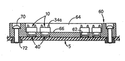
図1において、本発明の電気コネクタ組立体1は、コネクタモジュール(第1コネクタ)10、第2コネクタ40及びベースシェル(支持部材)60からなる。コネクタモジュール10は、液晶ポリマ等の樹脂材料で成形された略直方体状の第1絶縁ハウジング12、及びBe−Cu等のばね弾性を有する銅合金板を打抜き加工し、ニッケル、パラジウム及び金の各めっき層が形成された多数の平板状の第1コンタクト30を有する。第1絶縁ハウジング12は、その対向する側面14、16に第1コンタクト30の数に対応した第1キャビティ18が千鳥状に形成されている。各第1キャビティ18は、絶縁ハウジング12の上面20に連通する開口18a、第1コンタクト30の第1ばねアーム部34を収容するばね部収容部18b、第1コンタクト30の第1基部32を収容する基部収容部18c、第1コンタクト30の圧入部36を受容する圧入部受容部18d、及び第1コンタクト30の接続部38を収容する接続部収容部18eを有し、これらは互いに連通している。
【0014】
各第1コンタクト30は、第1基部32、この第1基部32の上方へ湾曲して延びる第1ばねアーム部(弾性接触部)34、第1基部32の側部から直線的に延びる圧入部36、及び第1基部32の下側角部から延びる接続部(第1接続部)38を有する。第1ばねアーム部34は、第1基板3との多数回の接続及び分離を保証するためにばね長を十分に長く設定されて応力の集中が回避されており、その自由端には幅広で且つ略円弧状の接触端34aが設けられている。接触端34aは、第1基板3の下面3b上に形成された導電性パッド4と当接すると破線で示される位置に変位するので、第1基板3の下面3bに沿って若干量のワイピングが得られる。圧入部36は、全体が槍状をなし、その根元近傍に圧入部受容部18dの内壁に食い込む1対の突起36aを有する。圧入部36とは反対側の第1基部32の平坦な側面32aは、第1コンタクト30を第1キャビィ18内に圧入する際に圧入治具(図示せず)との当接面となる。接続部38は、後述する第2コネクタ40の上側略半分を受容すると共に接触する凹部38aを有する。第1コンタクト30は第1絶縁ハウジング12に千鳥状に設けられた第1キャビティ18に挿入されるので、接触端34aは第1絶縁ハウジング12の上面20から千鳥状に突出する。
【0015】
第2コネクタ40は、適当な樹脂材料で成形された第2絶縁ハウジング42、及び各々がばね弾性を有する銅合金を打ち抜いて平板状に形成され、左右対称に配置された2列の平板状の第2コンタクト50を有する。第2絶縁ハウジング42は側面視略逆T字状をなし、上側略半分がコネクタモジュール10の下向きの凹部22内に挿入される。各第2コンタクト50は、基部52から上方に延びて第2ハウジング42の圧入部受容部44内に圧入される圧入部54、この圧入部54と離隔して基部52から略上方に延びる第2ばねアーム部(第2接続部)56、及び基部52から横方向に延びて第2基板5の上面5a上の導電性パッド6に半田接続される表面実装タイン部58を有する。第2基板5への接続部として表面実装タイン部58を採用したので、第2基板5の下面(裏面)5bに別の電子デバイスを実装するスペースが確保される。第2コネクタ40の上側略半分がコネクタモジュール10の凹部22内に挿入されると、左右対称に背向配置された第2コンタクト50の第2ばねアーム部56はコネクタモジュール10内の第1コンタクト30の接続部38の対向する側壁にそれぞれ接触する。単一の第1コンタクト30に対して2個の第2コンタクト50が接触するので、接触の冗長性があり、接触の信頼性が高い利点がある。
【0016】
図1及び図2において、ベースシェル60は、アルミニウムダイキャスト等の金属製の枠体であり、各コネクタモジュール10の下側突部24をそれぞれ受容する受容孔62、これらすべての受容孔62に連通すると共に上方に開口する凹部64を有する。凹部64には、コネクタモジュール10及び第1基板3が挿入される。凹部64の上面66は、コネクタモジュール10の下側角部26と当接する当接面を構成する。このため、実使用時において、第1コンタクト30の第1ばねアーム部34を弾性変形させる力は、剛性を有するベースシェル60の凹部上面66に伝達されるので、第2コンタクト50の表面実装タイン部58及び第2基板5のパッド6の間の半田接続部に伝達されない。従って、半田接続部に半田クラックが発生するおそれは実質的にない。さらに、第1コンタクト30の第1ばねアーム部34を弾性変形させる力は、比較的表面積が大きくて剛性を有する単一のベースシェル60が受けて第2基板5に伝達するので、第2基板5に反りは発生しない。また、ベースシェル60は、その周辺においてベースシェル60を第2基板5に固定するボルト70を受容するボルト受容孔68を有する。なお、ベースシェル60が第2基板5の上面5a上の回路を短絡させないように、ベースシェル60及び第2基板5間に絶縁シート74(図5参照)を介在させてもよい。
【0017】
次に、図2及び図3を参照して、本発明の電気コネクタ組立体の組立手順について説明する。まず、装置本体(図示せず)側の第2基板5の上面5aに多数の第2コネクタ40を表面実装する。次に、ベースシェル60の受容孔62内に第2コネクタ40を挿通させてベースシェル60を第2基板5の上面5a上に載置し、ボルト70及びナット72によりベースシェル60を第2基板5に固定する。続いて、多数のコネクタのモジュール10のそれぞれを各受容孔62内に挿入し、各第2コネクタ40と嵌合させる。これにより、装置本体側の組立は完了する。各コネクタモジュール10は、各第2コネクタ40と嵌合するのみで、第2基板5、第2コネクタ40又はベースシェル60にロックされていない。このため、例えばコネクタモジュール10の第1コンタクト30に不具合が生じた場合、コネクタモジュール10を第2コネクタ40から簡単に分離して故障した第1コンタクト30を容易に交換することができるので、メンテナンス性に優れている。また、第2基板5への第2コネクタ40の表面実装工程は、第2基板5へのベースシェル60の取付の前に行われるので、ベースシェル60は第2コネクタ40の半田付け検査の障害にならない。
【0018】
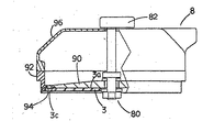
次に、図4を参照して、第1基板3を有するケーブル側組立体8について説明する。図4は、図1の電気コネクタ組立体に接続されるケーブル側組立体8を示す、一部を断面した正面図である。ケーブル側組立体8の構造は、基本的には図7に示される従来のケーブル側組立体160と同じである。即ち、例えば超音波変換器(図示せず)から延びるケーブル(図示せず)を終端するコネクタ(図示せず)を第1基板3に接続すると共に、駆動装置80のハンドル82を回転することにより第1基板3及び装置本体(図示せず)側の第2基板5(図1参照)を相互に接近する方向に付勢する。これにより、第1基板3及び第2基板5間を零挿入力で相互接続する。従来のケーブル側組立体160と異なる点は、第1基板3の上面(裏面)3a側に格子状の補強板90を配置して第1基板3を支持したことである。この補強板90はコネクタ製造業者が取付けるので、装置の製造業者に負担をかけることなく第1基板3の反りを防止することができる。補強板90は、金属ダイキャスト製のケーブル側ベースシェル92と一体に形成してもよい。ケーブル側ベースシェル92及び第1基板3には、装置本体側に設けられたガイドピン(図示せず)を受容する受容穴94、3cがそれぞれ形成され、第1基板3のパッド4及びコネクタモジュール10の接触端34aを整合させる。ベースシェル92の上方にはケーブルをクランプするコネクタシェル96が設けられる。なお、このシェル96を金属製にして電磁遮蔽の機能を付加してもよい。また、装置の仕様によっては、ケーブルを終端するコネクタを第1基板3に直接接続する代わりに、特定の電子回路を形成したFPC等を介して第1基板3に接続してもよい。この場合は第1基板3の裏面の実装の自由度が高い。
【0019】
以上、本発明の電気コネクタ組立体の好適な実施の形態について説明したが、本発明は上述の実施の形態に限定することなく、必要に応じて種々の変形又は変更をすることがきる。例えば、図5に示されるように、第1コンタクト30’の接続部を、対向する側部を有する雄型の接続部38’とし、対応する第2コネクタ40’の第2コンタクト50’を左右対称に対向配置してもよい。また、第1コンタクトの接続部を弾性を有する形状にし、第2コンタクトを剛性を有する形状にしてもよいし、さらに両者を弾性を有する形状にしてもよい。また、電気コネクタ組立体は、第1基板をICチップ又はICパッケージに代えることによりICテスタ等に用いてもよい。
【0020】
【発明の効果】
請求項1による電気コネクタ組立体によれば、第1絶縁ハウジングと、第1絶縁ハウジング内に収容され、一端に第1基板と当接する弾性接触部を有すると共に他端に第1接続部を有する第1コンタクトとからなる第1コネクタと、第2絶縁ハウジングと、第2絶縁ハウジング内に収容され、第1接続部に分離可能に接続される第2接続部を有すると共に第2基板に表面実装される第2コンタクトとからなる第2コネクタと、第2基板上に配置されると共に第1絶縁ハウジングを支持する支持部材とを具備するので、第2基板の裏面の実装スペース及び第1コンタクトの交換の容易さを確保しつつ、第2基板の反りを効果的に防止して接続の信頼性を向上させる利点がある。
【0021】
請求項2に係る零挿入力接続組立体によれば、請求項1の電気コネクタ組立体のほかに、第1及び第2基板、及び駆動装置を具備するので、第2基板の裏面の実装スペース及び第1コンタクトの交換の容易さを確保しつつ、第2基板の反りを効果的に防止して接続信頼性の高い零挿入力接続組立体が得られる。
【図面の簡単な説明】
【図1】本発明の電気コネクタ組立体の一実施形態を示す断面図である。
【図2】図1の電気コネクタ組立体の装置本体側の組立手順を示す概略断面図である。なお、コネクタモジュール及び第2コネクタは断面していない。
【図3】図2の部分の組立完了の状態を示す断面図である。なお、コネクタモジュール及び第2コネクタは断面していない。
【図4】図1の電気コネクタ組立体に接続されるケーブル側組立体を示す一部を断面した正面図である。
【図5】本発明の電気コネクタ組立体の別の実施形態を示す断面図である。
【図6】従来の電気コネクタを示す断面図である。
【図7】図6の電気コネクタを用いた零挿入力接続組立体を示す断面図である。
【図8】基板との接続状態における図6の電気コネクタを示す断面図である。
【符号の説明】
1 電気コネクタ組立体
3 第1基板
5 第2基板
10 第1コネクタ
12 第1ハウジング
30 第1コンタクト
34 弾性接触部
38 第1接続部
40 第2コネクタ
42 第2ハウジング
50 第2コンタクト
56 第2接続部
60 支持部材
80 駆動装置[0001]
BACKGROUND OF THE INVENTION
The present invention relates to an electrical connector assembly and a zero insertion force connection assembly using the same, and more specifically, an electrical connector assembly for interconnecting two boards in parallel with each other and a zero insertion force connection assembly using the same. About.
[0002]
[Prior art]
An electrical connector having an electrical connector called an interposer has been used to connect two substrates in parallel with each other at a high density and with a zero insertion force so that they can be connected and separated many times. As a typical example, an electrical connector shown in FIGS. 6 to 8 is known (see Japanese Patent Laid-Open No. 7-307188). The
[0003]
The
[0004]
[Problems to be solved by the invention]
In the conventional board-to-board zero insertion force connection structure using the electrical connector, there is an advantage that the boards can be connected with high density. However, since the reaction force of the force that elastically deforms the first and
[0005]
In order to prevent the
[0006]
It is also conceivable to replace the
[0007]
Therefore, it can be considered that only the connection between the electrical connector and the second substrate is changed to a connection using a compliant pin, a through-hole solder connection, or a surface mount solder connection. However, the former two have the problem that the problem of securing the mounting space on the back surface of the second substrate has not been solved. In the latter two cases, a force that elastically deforms the first spring portion of the contact is transmitted as unnecessary stress to the solder connection portion, and there is a possibility that a solder crack may occur. Furthermore, as a problem common to all of these, when the contacts are mounted at a high density, there is a problem that repair and replacement of the contacts are not easy when a failure occurs in the first spring portion of the contacts.
[0008]
Accordingly, the present invention is, while ensuring the ease of replacement of the mounting space及beauty co Ntakuto the back surface of the second substrate, the electrical connector arrangement for improving the reliability of the connection of the warp of the second substrate effectively prevented to The object is a solid body and a zero insertion force connection assembly using the same.
[0009]
[Means for Solving the Problems]
An electrical connector assembly according to claim 1 is an electrical connector assembly for interconnecting a first board and a second board in parallel to each other. The electrical connector assembly is housed in the first insulating housing and in the first insulating housing, A first connector comprising a first contact having an elastic contact portion in contact with the first substrate and having a first connection portion at the other end; a second insulation housing; and the second insulation housing. a second connector that Do and a second contact that is surface-mounted on the second substrate and having a second connecting portion that is detachably connected to the first connecting portion, wherein while being disposed on the second substrate first And 1 a support member for supporting the insulating housing. Here, the “substrate” includes not only a printed wiring board or a printed circuit board but also other electrical components such as an IC chip or an IC package.
[0010]
A zero insertion force connection assembly according to a second aspect is provided with the electrical connector assembly according to the first aspect, the first board, the second board, and the first and second boards in a direction approaching each other. It is characterized by comprising the drive device which energizes.
[0011]
DETAILED DESCRIPTION OF THE INVENTION
DESCRIPTION OF EXEMPLARY EMBODIMENTS Hereinafter, preferred embodiments of the invention will be described with reference to the accompanying drawings.
[0012]
FIG. 1 is a cross-sectional view showing an embodiment of the electrical connector assembly of the present invention. FIG. 2 is a schematic cross-sectional view showing an assembly procedure on the apparatus main body side of the electrical connector assembly of FIG. FIG. 3 is a cross-sectional view showing a state where the assembly of the portion of FIG. 2 is completed.
[0013]
In FIG. 1, an electrical connector assembly 1 of the present invention includes a connector module (first connector) 10, a
[0014]
Each
[0015]
The
[0016]
1 and 2, the
[0017]
Next, the assembly procedure of the electrical connector assembly according to the present invention will be described with reference to FIGS. First, a large number of
[0018]
Next, the
[0019]
The preferred embodiments of the electrical connector assembly of the present invention have been described above, but the present invention is not limited to the above-described embodiments, and various modifications or changes can be made as necessary. For example, as shown in FIG. 5, the connection portion of the
[0020]
【The invention's effect】
According to the electrical connector assembly of the first aspect, the first insulating housing, the elastic contact portion which is accommodated in the first insulating housing and contacts the first substrate at one end, and the first connection portion at the other end are provided. A first connector comprising a first contact, a second insulating housing, and a second connecting portion that is housed in the second insulating housing and is detachably connected to the first connecting portion and is surface-mounted on the second substrate And a support member disposed on the second substrate and supporting the first insulating housing, so that the mounting space on the back surface of the second substrate and the first contact There is an advantage that the reliability of connection is improved by effectively preventing warpage of the second substrate while ensuring the ease of replacement.
[0021]
According to the zero insertion force connecting assembly according to the second aspect, in addition to the electrical connector assembly according to the first aspect, the first and second substrates and the driving device are provided. In addition, it is possible to obtain a zero insertion force connection assembly with high connection reliability by effectively preventing warpage of the second substrate while ensuring easy replacement of the first contact.
[Brief description of the drawings]
FIG. 1 is a cross-sectional view showing an embodiment of an electrical connector assembly of the present invention.
2 is a schematic cross-sectional view showing an assembly procedure on the apparatus main body side of the electrical connector assembly of FIG. 1. FIG. The connector module and the second connector are not sectioned.
FIG. 3 is a cross-sectional view showing a state where the assembly of the portion of FIG. 2 is completed. The connector module and the second connector are not sectioned.
4 is a front view, partly in section, showing a cable side assembly connected to the electrical connector assembly of FIG. 1. FIG.
FIG. 5 is a cross-sectional view showing another embodiment of the electrical connector assembly of the present invention.
FIG. 6 is a cross-sectional view showing a conventional electrical connector.
7 is a cross-sectional view showing a zero insertion force connection assembly using the electrical connector of FIG. 6. FIG.
8 is a cross-sectional view showing the electrical connector of FIG. 6 in a connected state with a substrate.
[Explanation of symbols]
DESCRIPTION OF SYMBOLS 1
Claims (2)
第1絶縁ハウジングと、該第1絶縁ハウジング内に収容され、一端に前記第1基板と当接する弾性接触部を有すると共に他端に第1接続部を有する第1コンタクトとからなる第1コネクタと、
第2絶縁ハウジングと、該第2絶縁ハウジング内に収容され、前記第1接続部に分離可能に接続される第2接続部を有すると共に前記第2基板に表面実装される第2コンタクトとからなる第2コネクタと、
前記第2基板上に配置されると共に前記第1絶縁ハウジングを支持する支持部材と
を具備することを特徴とする電気コネクタ組立体。In an electrical connector assembly for interconnecting a first board and a second board in parallel to each other,
A first connector comprising a first insulating housing and a first contact housed in the first insulating housing and having an elastic contact portion in contact with the first substrate at one end and a first connection portion at the other end; ,
A second insulating housing; and a second contact that is accommodated in the second insulating housing and is separably connected to the first connecting portion and is surface-mounted on the second substrate. A second connector;
An electrical connector assembly comprising: a support member disposed on the second substrate and supporting the first insulating housing.
Priority Applications (2)
| Application Number | Priority Date | Filing Date | Title |
|---|---|---|---|
| JP06401898A JP3932151B2 (en) | 1998-02-27 | 1998-02-27 | Electrical connector assembly and zero insertion force connection assembly using the same |
| CN 99102532 CN1227434A (en) | 1998-02-27 | 1999-02-26 | Electrical connector assembly and zero insertion force connecting assembly using same |
Applications Claiming Priority (1)
| Application Number | Priority Date | Filing Date | Title |
|---|---|---|---|
| JP06401898A JP3932151B2 (en) | 1998-02-27 | 1998-02-27 | Electrical connector assembly and zero insertion force connection assembly using the same |
Publications (2)
| Publication Number | Publication Date |
|---|---|
| JPH11251016A JPH11251016A (en) | 1999-09-17 |
| JP3932151B2 true JP3932151B2 (en) | 2007-06-20 |
Family
ID=13246013
Family Applications (1)
| Application Number | Title | Priority Date | Filing Date |
|---|---|---|---|
| JP06401898A Expired - Fee Related JP3932151B2 (en) | 1998-02-27 | 1998-02-27 | Electrical connector assembly and zero insertion force connection assembly using the same |
Country Status (2)
| Country | Link |
|---|---|
| JP (1) | JP3932151B2 (en) |
| CN (1) | CN1227434A (en) |
Families Citing this family (2)
| Publication number | Priority date | Publication date | Assignee | Title |
|---|---|---|---|---|
| TW529208B (en) * | 2000-10-13 | 2003-04-21 | J S T Mfg Co Ltd | Electric connector and electric connector with cap |
| DE202014011449U1 (en) | 2013-12-12 | 2020-10-26 | Harting Electric Gmbh & Co. Kg | Holding frame for a connector |
-
1998
- 1998-02-27 JP JP06401898A patent/JP3932151B2/en not_active Expired - Fee Related
-
1999
- 1999-02-26 CN CN 99102532 patent/CN1227434A/en active Pending
Also Published As
| Publication number | Publication date |
|---|---|
| CN1227434A (en) | 1999-09-01 |
| JPH11251016A (en) | 1999-09-17 |
Similar Documents
| Publication | Publication Date | Title |
|---|---|---|
| CN109818170B (en) | Socket connector for electronic package | |
| JP3169821U (en) | Electrical card edge connector | |
| US7125260B2 (en) | Mounting structure of connector | |
| JP3035291B2 (en) | High-speed backplane connector | |
| US7179091B2 (en) | Edge mount electrical connector | |
| US7575443B2 (en) | Combined fastening and contacting system for electrical components on superimposed circuit boards | |
| JP2937728B2 (en) | Printed wiring board connector | |
| JP4863130B2 (en) | Board connector, semiconductor device socket including the same, cable connector, and board-to-board connector | |
| US7972149B2 (en) | Board with connection terminals | |
| JP2017103223A (en) | Rigid-flex circuit connector | |
| JPH08330032A (en) | Connector for circuit board | |
| US6392887B1 (en) | PLGA-BGA socket using elastomer connectors | |
| JPH09506734A (en) | Connector for high density electronic assembly | |
| US7341460B1 (en) | Electrical connector | |
| TW540190B (en) | Connector for plate object with terminals | |
| US20050245106A1 (en) | Land grid array-pin grid array connector | |
| JP4808032B2 (en) | Compressive load adaptable socket | |
| US7692281B2 (en) | Land grid array module with contact locating features | |
| TW201203725A (en) | Mounting component, electronic device and mounting method | |
| JP3932151B2 (en) | Electrical connector assembly and zero insertion force connection assembly using the same | |
| US8272880B2 (en) | Socket and semiconductor device including socket and semiconductor package | |
| US8083529B2 (en) | Socket | |
| JP2019200872A (en) | connector | |
| JP2009193677A (en) | Adapter, socket, electronic device, and mounting method | |
| CN115411539A (en) | Power connector assembly |
Legal Events
| Date | Code | Title | Description |
|---|---|---|---|
| A521 | Written amendment |
Free format text: JAPANESE INTERMEDIATE CODE: A523 Effective date: 20050224 |
|
| A621 | Written request for application examination |
Free format text: JAPANESE INTERMEDIATE CODE: A621 Effective date: 20050224 |
|
| A977 | Report on retrieval |
Free format text: JAPANESE INTERMEDIATE CODE: A971007 Effective date: 20060210 |
|
| A131 | Notification of reasons for refusal |
Free format text: JAPANESE INTERMEDIATE CODE: A131 Effective date: 20060313 |
|
| A521 | Written amendment |
Free format text: JAPANESE INTERMEDIATE CODE: A523 Effective date: 20060512 |
|
| A131 | Notification of reasons for refusal |
Free format text: JAPANESE INTERMEDIATE CODE: A131 Effective date: 20061005 |
|
| A521 | Written amendment |
Free format text: JAPANESE INTERMEDIATE CODE: A523 Effective date: 20061204 |
|
| TRDD | Decision of grant or rejection written | ||
| A01 | Written decision to grant a patent or to grant a registration (utility model) |
Free format text: JAPANESE INTERMEDIATE CODE: A01 Effective date: 20070309 |
|
| A61 | First payment of annual fees (during grant procedure) |
Free format text: JAPANESE INTERMEDIATE CODE: A61 Effective date: 20070309 |
|
| R150 | Certificate of patent or registration of utility model |
Free format text: JAPANESE INTERMEDIATE CODE: R150 |
|
| LAPS | Cancellation because of no payment of annual fees |