JP3930116B2 - Computer system - Google Patents
Computer system Download PDFInfo
- Publication number
- JP3930116B2 JP3930116B2 JP23428597A JP23428597A JP3930116B2 JP 3930116 B2 JP3930116 B2 JP 3930116B2 JP 23428597 A JP23428597 A JP 23428597A JP 23428597 A JP23428597 A JP 23428597A JP 3930116 B2 JP3930116 B2 JP 3930116B2
- Authority
- JP
- Japan
- Prior art keywords
- cpu
- mode
- sequence
- interrupt
- smi
- Prior art date
- Legal status (The legal status is an assumption and is not a legal conclusion. Google has not performed a legal analysis and makes no representation as to the accuracy of the status listed.)
- Expired - Lifetime
Links
Images


Description
【0001】
【発明の属する技術分野】
この発明は、コンピュータシステムの割り込み制御処理に係わり、特に、その割り込み制御処理中での各処理の並列化に関する。
【0002】
【従来の技術】
近年、携帯が容易でバッテリーにより動作可能なラップトップタイプまたはノートブックタイプのパーソナルコンピュータが種々開発される。このパーソナルコンピュータの割り込み制御処理、例えば、現在の動作環境を保存し、次回コンピュータシステムの起動時に動作環境をもとに戻すラピットレジューム/サスペンド処理や、ドッキングステーションやデバイスベイ対応の外部デバイスをコンピュータシステムの通電中に接続及び切り離すドック/アンドック処理は、オペレーティングシステム(以下、OSと称す)動作中の割り込み制御処理として実行された。
【0003】
従来技術の割り込み制御処理の手順は、コンピュータシステム内蔵の電源マイコンが電源スイッチが押圧されたことを検出した場合、電源マイコンは割り込み要求線を通じて割り込み制御ロジックに対して割り込み要求を発行する。又は、OS動作中にドッキングステーションがコンピュータシステム本体の拡張バスコネクタ及び拡張デバイスがデバイスベイにドッキングした場合、同様に、ドッキングの制御を行う各回路は割り込み制御ロジックに対して割り込み要求を発行する。
【0004】
割り込み制御ロジックは、前記割り込み要求を受信後、中央処理装置(以下、CPUと称す)に対してシステムマネージメント割り込み(以下、SMIと称す)を発行する。
【0005】
CPUがSMI信号受信後、CPUの動作モードをシステムマネージメントモード(以下、SMMと称する)に移行し、BIOS―ROMに格納されている割り込み制御処理を起動する。割り込み制御処理は、CPUに要求された割り込み信号に対応した割り込み制御処理を実行する。
【0006】
ここで、SMMとは、米国インテル社製造のCPUに於いて、コンピュータシステムからCPUへSMI#信号が入力された場合、CPUがBIOS―ROM内の割り込み制御処理に移行するときに設定されるCPUの動作モードである。
【0007】
CPUが、SMM中に入っている間、コンピュータシステムからCPUに対して新たに割り込み(IRQ、INTRやSMI等)を要求することが出来ない。従って、割り込み制御処理は、一連の処理を直接的に実行しなければならず、各種I/Oデバイスに発行した所定のコマンド処理で時間待ちが必要な場合、割り込み制御処理中の他の処理を実行できず、時間待ちを行う必要があった。
【0008】
次に、割り込み制御処理の例として、図10に示される通り、ラピットサスペンド処理を説明する。ラピットサスペンド処理は、以下の5つの処理から構成される。
【0009】
(1)パネルライトオフシーケンス処理(S600)
(2)HDDモータオフシーケンス処理(S610)
(3)各種I/Oデバイスのレジスタ保存シーケンス処理(S620)
(4)メモリチェックサム(S630)
(5)フラッシュROM書き換え(S640)
ここで、(1)〜(3)のシーケンス処理に於いては、コマンドを受信した各種I/Oデバイスがそのコマンドに対応する処理を完了するまでにはある一定時間が必要となる。各シーケンスの処理が完了しない限り、次のシーケンスを実行することは出来ない。
【0010】
このように、各シーケンスの処理に於いては、そのデバイスのコマンド処理に要する時間だけ、次のシーケンス処理のタイミングが遅延されることになる。従って、SMMを用いたシステムの割り込み制御処理(ラピットサスペンド処理)を実行する時間は、各シーケンス処理のコマンドに対応する時間(待ち時間を含む)の総和となり、多くの時間が要した。
【0011】
更に、上記ラピットサスペンド処理中に、コンピュータシステムのI/Oデバイス(電源マイコン)からの電源オフ・オンの要求を受け付けるために、ラピットサスペンド処理中に電源マイコンからの要求の有無をポーリング(S660)してチェックしていたので、タイムリーな処理ができなかった。
【0012】
【発明が解決しようとする課題】
上記した従来技術では、SMM中で割り込み制御処理を実行する場合、他の割り込み要求を受け付けられないので、割り込み制御処理に時間がかかるという問題があった。
【0013】
また、割り込み制御処理中に他のI/Oデバイスからの割り込み要求が受け付けられないので、各種I/Oデバイスに対してポーリングして要求の有無をチェックする別途特別な処理を必要としていた。
【0014】
そこで、本発明は上記の問題を解決するためになされたものであり、割り込み要求を受付ないSMMで、CPUの動作モードを割り込み可能とし、割り込み制御処理中で必要な処理を並列化することにより割り込み制御処理全体の処理時間の短縮を提供することを目的とする。
【0015】
【課題を解決するための手段】
この発明は、割り込み要求を受付ないシステム管理モードで所定の処理を実行するコンピュータシステムに於いて、OSの動作中にシステム管理割り込み要求を発生する手段と、第1のシステム管理割り込み要求に応答して、CPUの動作モードを前記システム管理モードに変更する手段と、前記CPUの動作モードが前記システム管理モードに変更された後、前記CPUの動作モードを、割り込み要求の受付が可能な割り込み受付可能モードに設定する手段と、前記割り込み受付可能モードで割り込み制御処理を構成する複数の処理の動作を個々に管理するための複数のテーブルを用いることにより当該複数の処理を並列して実行する手段とを具備し、前記CPUの動作モードを前記割り込み受付可能モードに設定する手段は、第2のシステム管理割り込み要求に応答して、CPUステートマップ情報を前記メモリの第2のエリアに保存する手段を具備し、前記CPUの動作モードを前記割り込み受付可能モードに設定する手段は、更に、前記メモリ中の前記第1のエリアに保存された前記CPUステートマップ情報と前記第2のエリアに保存された前記CPUステートマップ情報とを入れ替える手段を具備することを特徴とする。
【0016】
このような構成によれば、システムの初期化時、CPUステートマップ情報をメモリ上に保存することによって、OS起動中にシステム管理割り込み要求を受けた場合、CPUの動作モードをシステム管理モードから割り込み可能なモードへ変更し、割り込み制御処理を割り込み可能なモードで実行することによって、割り込み制御処理中で必要な処理を並列化することができ、割り込み制御処理全体の処理時間を短縮することができる。
【0017】
【発明の実施の形態】
以下、図面を参照してこの発明の実施形態を説明する。
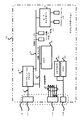
図1には、この発明の一実施形態に係るコンピュータシステムの構成が示される。このコンピュータシステムは、バッテリ駆動可能なノートブックタイプまたはラップトップタイプのポータブルコンピュータであり、そのシステムボード上には、プロセッサバス1、内部PCIバス2、内部ISAバス3、およびI2Cバス4が配設される。また、このポータブルコンピュータ本体に設けられたドッキングコネクタ10には、機能拡張のための拡張ユニットとして、図2のドッキングステーション30がユーザによって必要に応じて接続される。ドッキングコネクタ10は、図示のように、3つのコネクタ要素101,102,103から構成される。
【0018】
コンピュータ本体内に、CPU11、ホスト−PCIブリッジ装置12、メモリ13、ディスプレイコントローラ14、DSPインタフェースゲートアレイ(以下、DSP IF GAと称す)15、内部PCI−ISAブリッジ装置16、デバイスベイコントローラ17、PCI−DS(DS:ドッキングステーション)ブリッジ装置18、BIOS―ROM19、ハードディスクドライブ20、キーボードコントローラ21、リアルタイムクロック(以下、RTCと称す)22、I/Oコントロールゲートアレイ23、電源コントローラ(以下、PSCと称す)24などが設けられる。
【0019】
ドッキングステーション30は、PCI拡張カード、ISA拡張カード、PCカード、ハードディスクドライブ、CD−ROMドライブなどの拡張デバイスの増設のために使用されるものであり、このドッキングステーション30内には、図2に示されているように、外部PCIバス5および外部ISAバス6が拡張バスとして配設されており、そこにはPCI拡張スロットおよびISA拡張スロットなどが接続される。ここでは、この外部ISAバス6にハードディスクドライブ36が接続される。
【0020】
また、このドッキングステーション30内には、DS−PCI/ISAブリッジ装置31、DSコントローラ33、EEPROM34なども設けられる。
次に、図1のコンピュータ本体に設けられた各コンポーネントの機能および構成について説明する。
【0021】
CPU11は、たとえば、米インテル社によって製造販売されているマイクロプロセッサ“pentium”などによって実現される。このCPU11の入出力ピンに直結されているプロセッサバス1は、64ビット幅のデータバスを有す。
【0022】
ホスト−PCIブリッジ装置12は、プロセッサバス1と内部PCIバス2との間を繋ぐブリッジLSIであり、PCIバス2のバスマスタの1つとして機能する。このホスト−PCIブリッジ装置12は、プロセッサバス1と内部PCIバス2との間で、データおよびアドレスを含むバスサイクルを双方向で変換する機能、およびメモリバスを介してメモリ13をアクセス制御する機能などを有す。
【0023】
更に、ホスト−PCIブリッジ装置12は、CPU11に対する割り込みを発行する割り込み制御回路を内蔵し、該回路はSMI発生回路121、SMI要因レジスタ122、ソフトSMIタイマーイネーブルレジスタ123と、カウンタレジスタ124から構成される。
【0024】
SMI発生回路121は、電源スイッチのオン/オフ動作、ドッキングステーションのドック/アンドック動作、ホットキーからのH/W割り込みに応じてCPU11のSMI#ピンに対してSMI#信号を発行する。
【0025】
SMI要因レジスタ122は、SMI発生回路121に接続され、SMI発生の要因を識別するためのレジスタであり、ここでは、電源スイッチのオン/オフ動作、ドッキングステーションのドック/アンドック動作、ホットキーからのH/W割り込みの状態を示すステータスビットを格納する。
【0026】
ソフトSMIタイマーイネーブルレジスタ123は、カウンタレジスタ1123のダウンカウントの開始をイネーブルするレジスタである。
カウンタレジスタ124は、後述する各シーケンステーブルのうち、次回起動時間が最も早い時刻から現在の時間を引いた値が設定され、カウンタ値が“0”に達した時、CPU11に対してSMI#信号を発行する。
【0027】
メモリ13は、オペレーティングシステム、デバイスドライバ、実行対象のアプリケーションプログラム、および処理データなどを格納するメモリデバイスであり、複数のDRAMモジュールによって構成される。
【0028】
また、このメモリ13は、システムボード上に予め実装されるシステムメモリ131と、システムメモリの一部として使用されるSM−RAM132から構成される。
【0029】
これらシステムメモリ131およびSM−RAM132を構成するDRAMモジュールとしては、シンクロナスDRAMやRambusなど、バンク毎にメモリクロックの供給が必要な高速メモリが利用される。
【0030】
SM−RAM132には、不揮発性メモリ又はバックアップされた64kバイトメモリで構成され、後述するCPUステートマップを格納するエリアA及びエリアBや割り込み制御処理の並列化を行う為のシーケンステーブルの各々が設けられる。
【0031】
更に、SM−RAM132には、ユーザがシステム起動時に入力したパスワード情報やSMM起動時のSM−BIOS19への飛び先を指定するSMIハンドラーを格納する。
【0032】
このメモリ13は、32ビット幅または64ビット幅のデータバスを有する専用のメモリバスを介してホスト−PCIブリッジ装置12に接続される。メモリバスのデータバスとしてはプロセッサバス1のデータバスを利用することもできる。この場合、メモリバスは、アドレスバスと各種メモリ制御信号線とから構成される。
【0033】
内部PCIバス2はクロック同期型の入出力バスであり、内部PCIバス2上の全てのサイクルはPCIバスクロックに同期して行われる。PCIバスクロックの周波数は最大33MHZ である。PCIバス2は、時分割的に使用されるアドレス/データバスを有す。このアドレス/データバスは、32ビット幅である。
【0034】
PCIバス2上のデータ転送サイクルは、アドレスフェーズとそれに後続する1以上のデータフェーズとから構成される。アドレスフェーズにおいてはアドレスおよび転送タイプが出力され、データフェーズでは8ビット、16ビット、24ビットまたは32ビットのデータが出力される。
【0035】
デイスプレイコントローラ14は、ホストーPCIブリッジ装置12と同様にPCIバス2のバスマスタの1つであり、ビデオメモリ(VRAM)143の画像データをLCD141や外部のCRTディスプレイ142に表示する。
【0036】
DSPインタフェースゲートアレイ15は、PCIデバイスの1つであり、DSP151、モデム(CODEC)152、およびサウンドCODEC153と共同して各種サウンド処理や電話/データの通信処理を行なうためのDSPシステムを構成する。
【0037】
このDSPインタフェースゲートアレイ15は、メモリ13に読み込まれて実行される専用のデバイスドライバプログラムの制御の下でDSP151、MODEM(CODEC)152、およびサウンドCODEC153と通信して、DSP151のデジタル信号処理機能を利用したサウンド処理や通信処理を制御する。
【0038】
内部PCI−ISAブリッジ装置16は、内部PCIバス2と内部ISAバス3との間を繋ぐブリッジLSIであり、PCIデバイスの1つとして機能する。この内部PCI−ISAブリッジ装置16には、PCIバスアービタ、およびDMAコントローラなどが内蔵される。内部ISAバス3には、BIOS―ROM19、HDD20、キーボードコントローラ21、RTC22、I/Oコントロールゲートアレイ23が接続される。
【0039】
デバイスベイコントローラ17は、PCIデバイスの1つであり、ドッキングされたデバイスベイ仕様の外部拡張デバイスを制御する。
PCI−DSブリッジ装置18は、ドッキングステーション30との間でバスの接続および切断を制御する。すなわち、PCI−DSブリッジ装置18は、内部PCIバス2とPCIバス相当のドッキングバスとを繋ぐブリッジLSIであり、PCIデバイスの1つとして機能する。このドッキングバス7は、ドッキングコネクタ10のコネクタ要素101を介して外部に導出され、ドッキングステーション30に接続される。
【0040】
BIOS―ROM19は、システムBIOS(Basic I/O System)を記憶するためのものであり、プログラム書き替えが可能なようにフラッシュメモリ(EEPROM)によって構成される。このシステムBIOSには、システムブート時に実行されるIRTルーチン(POST)と、各種I/Oデバイスを制御するためのデバイスドライバ(ランタイム)と、割り込み制御処理を実行するシステム管理プログラム(SM−BIOS)と、セットアップルーチンやユーザが設定したパスワード情報が含まれる。
【0041】
システム管理プログラムは、SMMにおいて実行される割り込みプログラムであり、SMIハンドラー、およびホットキー処理ルーチンなどの各種SMIサービスルーチンを含む。SMIハンドラーは、SMIの発生要因に応じてSMIサービスルーチンを起動するためのものであり、ホットキーによるSMIが発生した場合にはホットキー処理ルーチンを起動し、他の要因によるSMIが発生した場合にはその要因に対応するSMIサービスルーチンを起動する。本願発明の実施形態に於いては、SM−BIOSは、I/Oトラップ命令とソフトSMIタイマーによりCPU11にSMI#信号を発行し、SMIサービスルーチンから割り込み制御処理を実行する。
【0042】
ハードディスクドライブ(HDD)20は、内部ISAバス3に接続され、オペレーティングシステム(以降、OSと称す)を格納したプライマリーなHDDであり、このハードディスクドライブ20はアクセスロック機構によりアクセスロック状態である。更に、ハードディスクドライブ20は、システムとの入出力を制御するハードディスクコントローラと、パスワードを格納するメモリと、コンピュータシステムのデータを格納可能なメディアから構成される。
【0043】
I/Oコントロールゲートアレイ23は、内部ISAバス3とI2Cバス4とを繋ぐブリッジLSIであり、CPU11によってリード/ライト可能な複数のレジスタ群を内蔵する。これらレジスタ群を使用することにより、CPU11とI2Cバス4上の電源コントローラ24やDSコントローラ33との通信が可能となる。
【0044】
このI/Oコントロールゲートアレイ23からは、ドッキングステーション30と接続される制御信号線がドッキングコネクタ10のコネクタ要素102を介して複数本外部に導出される。また、I/Oコントロールゲートアレイ23は、コンピュータ本体とドッキングステーション30とのドッキング/アンドッキングを検出し、さらにコンピュータ本体が電源オン状態のままでドッキングステーション30の接続が行われたときに、活線挿抜などによってドッキングステーション30内の拡張ユニットの破壊やシステムの誤動作が生じないように制御する。
【0045】
更に、I/Oコントロールゲートアレイ23は、割り込みレジスタ231を内蔵し、電源スイッチのオン/オフを示すデータを電源コントローラ24経由およびドッキングステーション30内のドッキング/アンドックを示すデータをDSコントローラ33経由で設定される。
【0046】
I2Cバス4は、1本のクロック信号線と1本のデータ線(SDA)から構成される双方向バスであり、これはドッキングコネクタ10のコネクタ要素103を介して外部に導出される。
【0047】
電源コントローラ24は、電源スイッチのオン/オフなどに応じてコンピュータ本体をパワーオン/パワーオフするためのものであり、また、ドッキングステーション30とのドック/アンドック応じた電源制御も行う。
【0048】
次に、図2のドッキングステーション30のコンポーネントについて説明する。
前述したように、ドッキングステーション30は、ポータブルコンピュータ本体に取り外し可能に装着できる拡張ユニットである。図3はコンピュータ本体がドッキングステーション30に装着される様子を示すものである。
【0049】
このような外観を持つドッキングステーション30内部に設けられたDS−PCI/ISAブリッジ装置31は、コンピュータ本体からドッキングステーション30に導出されるドッキングバス7と外部PCIバス5および外部ISAバス6とを繋ぐブリッジLSIである。このDS−PCI/ISAブリッジ装置31はPCIデバイスの1つである。
【0050】
DSコントローラ33は、ドッキングステーション30の電源のオン/オフ、およびポータブルコンピュータ本体とドッキングステーション30とのドッキング/アンドッキングを制御するためのマイコンであり、I2Cバス4を使用してコンピュータ本体のI/Oコントロールゲートアレイ23と通信する。
【0051】
EEPROM34は、ドッキングステーション30の拡張スロットに装着されている拡張カードなどの属性(アドレス、DMAチャンネル、IRQ番号、その他)など、プラグ・アンド・プレイ(Plug and Play)に必要なPnP情報が格納される。このPnP情報は、コンピュータ本体とドッキングステーション30とがドッキングされた時や、コンピュータ本体又はドッキングステーション30のパワーオン時などに、BIOS―ROM19のシステムBIOSの制御の下、I2Cバス4を介してI/Oコントロールゲートアレイ23によってEEPROM34からリードされる。
【0052】
カードコントローラ35は、コンピュータ本体内のカードコントローラ17と同様に、PCMCIA/カードバス準拠のPCカードを制御する。
次に、図4と図5のフローチャートと図6のCPUメモリマップを参照して、図1のコンピュータシステムの電源投入時(初期化処理時)の動作について説明する。
【0053】
図1のコンピュータシステムがパワーオンされると、CPU11はリセットされ、リアルモードで動作を開始する(S210)。システムパワーオン時には、BIOS―ROM19内のシステムBIOSがCPUメモリアドレスF0000〜FFFFFに割当てられており、CPU11は、アドレスFFFF0の命令をフェッチする。これにより、システムBIOSのPOST(Power On Self Test)ルーチンの実行がリアルモード環境で開始される。
【0054】
POSTルーチンは、CPU11のMSWレジスタの設定などによってCPU11の動作モードをリアルモードに変更する(S220)。この後、プロテクトモードにおいて、コンピュータシステムの各種ゲートアレイ等の初期化処理やシステムメモリ131/SM−RAM132のリード/ライトコンペアチェックを実行する(S230〜240)。
【0055】
次に、図6に示される通り、SM−RAM132は、POSTルーチンの初期化開始時、SM−BASEレジスタによって、30000Hに割り付けられており、CPU11にSMI#信号が発行された際のSM−BIOSへのファージャンプ先を設定する為に、38000Hに割り付けられたSMIハンドラーにファージャンプ先の設定を実行する(S250)。
【0056】
POSTルーチンは、CPU11に対するSMI#信号発行後のSM−RAM132のCPUメモリマップの割り付け変更の為に、SMI発生回路121のイネーブル化を行い、SMI発生回路からCPU11に対するSMI#信号を発行可能とする(S310)。
【0057】
POSTルーチンは、CPUのAHレジスタにBIOSファンクションコールを設定し、特定のI/Oアドレスで割り込みトラップを仕掛け、CPU11に対してSMI#信号(以下、I/OトラップSMIと称す)を発行する(S320)。
【0058】
CPU11に対するSMI#信号発行に伴い、割込み発生時のCPUステートマップが3FE00H以降512Kバイトに自動的に格納され、SMIハンドラーが呼び出される。SMIハンドラーは、SMIハンドラーに設定されたファージャンプ先のSM−BIOSを起動し、SM−RAM132のCPUメモリマップの割り付け変更を実行する。
【0059】
ここで、CPUステートマップとは、CPU11にSMI#信号を発行して、CPU11の動作モードをSMMに移行する際、SMI#信号発行時のCPUの現在の状態をSM−RAM132内の所定エリアに保存し、SMMから抜ける際に、前記エリアに保存していた情報をCPU11にストアーするために使用される。
【0060】
SM−BIOSは、SM−BASEレジスタ値をFFFE0000Hに書き換える(S330)。SM―BASEレジスタ値の書き換えで設定されたSM−RAM132のCPUメモリマップは、図6に示される通り、FFFE0000H以降の64Kバイトに割り付けられる。
【0061】
SM−BIOSは、SM−BASEレジスタの値を書換え後、RSM命令を実行し、以降のSMI#信号の発生を禁止する(S340〜S350)。
SM−BASEレジスタ値の書換え割り込み処理から復帰したPOSTルーチンは、CPU11が割り込み可能な独自モードを作成する為、3FE00H以降512Kバイトに格納されたCPUステートマップをSM−RAM132のFFFEFE00H以降の512バイトのエリアBに書き込む(S270)。
【0062】
ここで、CPU11が割り込み可能な独自モードとは、SMIを含めた全割り込み(IRQ、NMI等)が可能であり、その割り込みをシステムBIOSが管理可能な状態である。
【0063】
次に、POSTルーチンは、OS起動後、 SMI発生回路からCPU11に対するSMI#信号を発行可能とする為、SMI発生回路121のイネーブル化を実行し、各種デバイスの初期化(各種デバイスへの既定値設定)を実行する(S280〜S290)。
【0064】
各種デバイスの既定値設定処理終了後、POSTルーチンは、CPU11のMSWレジスタの設定などによってCPU11の動作モードをプロテクトモードからリアルモードに変更し、OSを起動する(S300)。
【0065】
次に、図7のフローチャートを参照して、OS起動中の割り込み制御処理の動作を説明する。
システムBIOSのPOSTルーチン完了後、OSに制御を移行した後、サスペンド/レジューム要求の発生、又は、デスクステーションのドッキング/アンドッキング要求の発生、即ち、I/Oコントロールゲートアレイ23内の割り込みレジスタ231に電源スイッチのオン/オフ、又は、ドッキングステーション30のドック/アンドックの状態変化を設定すると、ポイント−ポイントの割り込み線を介してSMI発生回路121にSMI#信号発行を要求する。SMI発生回路121は、SMI要因レジスタ122に対応する要因ビットを設定し、CPU11に対してSMI#信号を発行する。
【0066】
CPU11がSMI#信号を受信すると、CPU11の動作モードをSMMに変更し、割り込み時のCPUステートをSM−RAM内のエリアBに格納する(S410)。
【0067】
次に、SM−RAM内のSMIハンドラーに設定されたファージャンプ先のSM―BIOSが起動され、SM−BIOSは、SMI発生要因のチェックを行う。SM―BIOSは、SMI要因レジスタ122の内容をチェックし、もしSM−BIOSが電源スイッチのオン/オフ動作に伴う状態変化であると判断したならば、SM−RAM132のエリアBに格納されたCPUステートマップ情報を初期化時保存したエリアAのCPUステートマップ情報と相互に入れ替える(S420〜S430)。
【0068】
CPU11の動作モードを独自モードに切り替え、ラピットサスペンド処理を並列処理する為、SM−BIOSは、初期化時設定したCPUステートマップ情報中のプログラムカウンタ(以降、PCと称す)の値をラピットサスペンド処理が格納されたBIOS―ROM番地に設定し、RSM命令を実行する。CPU11は、RSM命令に応答して、SM−RAM132内のエリアBに格納されたCPUステートマップ情報をCPU11内の各レジスタにリストアーする(S440)。
【0069】
CPU11が独自モードに変更後、CPU11のPCに設定されたアドレス値から次の命令を実行し、図8に示された通り、後述するラピットサスペンド処理の並列化を実行する(S450)。
【0070】
ラピットサスペンド処理の並列化実行終了後、システムBIOSはI/OトラップSMIをCPU11に発行する。システムBIOSは、このSMI#信号を発行する前に、CPU11のAHレジスタにSMMモードでのBIOSファンクションを設定する(S460)。
【0071】
CPU11がSMMモードに遷移後、SM−BIOSが起動される。SM−BIOSは、SMI要因レジスタ122をチェックし、SMI発生の要因を確認する。SM−BIOSは、SMIがI/OトラップSMIで発行されたことを確認後、CPUステートマップ情報が格納されたエリアBのAHレジスタの値を確認し、SM―BIOSは、独自モードからのSMI発行と判断し、SM−RAM132内のエリアBに格納されたCPUステートマップ情報をエリアAの内容と相互に入れ替える(S470)。
【0072】
SM−BIOSは、RSM命令を実行後、SM−RAM132内のエリアBに格納されたCPUステートマップ情報をCPU11にリストアーし、ラピットサスペンド処理に係わる割り込み制御処理の全て終了する(S480)。
【0073】
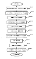
次に、図8のCPU処理の進行状況タイミング、図9のシーケンステーブル内の各ワーキングエリア情報と、図10の各シーケンス処理のフローチャートを参照して、割り込みを用いた並列処理の動作を説明する。
【0074】
システムBIOSは、ラピットサスペンド処理のパネルオフシーケンス処理を起動する為に、CPU11のAHレジスタにBIOSファンクションを設定し、I/OトラップSMIをCPU11に発行する(S500)。
【0075】
CPU11の動作モードが、SMMに遷移後、パネルオフシーケンス処理が呼び出される。パネルオフシーケンス処理は、初めに、電源コントローラ24のビジーチェックを要求する(S510)。電源コントローラ24のビジーチェックは、所定インターバル(待ち時間)を費やすので、パネルオフシーケンス処理は電源コントローラ24のビジーチェック要求後、SM−RAM132内のシーケンステーブル125に現在のプログラムカウンタ値“A”、パネルオフシーケンス処理が動作中であることを示すフラグと、インターバルタイマ値(次回起動時間:インターバル1)を設定する(S520)。
【0076】
パネルオフシーケンス処理は、各シーケンステーブル125内の次回起動時間の値を読み出し、最も早い起動時間のシーケンスを判断し、現在時刻から選択された最も早い起動時間を引いた値をカウンタレジスタ124に設定する(S530〜S550)。この場合、パネルオフシーケンス処理の動作フラグしか立っていないので、最も早い次回起動時間は、パネルオフシーケンスの起動時間である。
【0077】
カウンタレジスタ124に次回起動時間を設定後、パネルオフシーケンス処理は、SMIタイマーイネーブルレジスタ123を設定し、カウンタレジスタ124のダウンカウントを開始する(S560)。
【0078】
パネルオフシーケンス処理は、RSM命令を実行して、ラピットサスペンド処理のメインルーチンに復帰する(S570)。
ラピットサスペンド処理のメインルーチンに復帰後、ラピットサスペンド処理は、CPU11のAHレジスタにSM−BIOSファンクションを設定後、I/OトラップSMIをCPU11に発行して、HDDモータオフシーケンス処理を起動する(S500)。
【0079】
起動されたHDDモータオフシーケンス処理は、最初に、HDD20内蔵のハードディスクコントローラのビジーチェックを要求する(S510)。ハードディスクコントローラのビジーチェックは、所定インターバル(待ち時間)を費やすので、HDDモータオフシーケンス処理はハードディスクコントローラのビジーチェック要求後、SM−RAM132内のシーケンステーブル125に現在のプログラムカウンタ値“B”、ハードディスクコントローラオフシーケンス処理が動作中であることを示すフラグと、インターバルタイマ値(次回起動時間:インターバル1)を設定する(S520)。
【0080】
ハードディスクコントローラオフシーケンス処理は、各シーケンステーブル内の次回起動時間の値を読み出し、最も早い起動時間のシーケンスを判断し、現在時刻から選択された最も早い起動時間を引いた値をカウンタレジスタ124に設定する(S530〜S550)。この場合、パネルオフシーケンス処理の次回起動時間の方が、HDDモータオフシーケンス処理の次回起動時間より早いので、最も早い次回起動時間は、パネルオフシーケンスの起動時間である。
【0081】
HDDモータオフシーケンス処理は、カウンタレジスタ124にパネルオフシーケンスの次回起動時間を設定後、SMIタイマーイネーブルレジスタ123を設定し、カウンタレジスタ125のダウンカウントを開始する(S560)。
【0082】
HDDモータオフシーケンス処理は、RSM命令を実行して、ラピットサスペンド処理のメインルーチンに復帰する(S570)。
ラピットサスペンド処理のメインルーチンに復帰後、ラピットサスペンド処理は、CPU11のAHレジスタにSM−BIOSファンクションを設定後、I/OトラップSMIをCPU11に発行して、各種I/Oレジスタの保存シーケンス処理を起動する(S500)。
【0083】
各種I/Oレジスタの保存シーケンス処理は、各種I/Oレジスタに格納されているデータの出力を要求する為にコマンドを発行する(S510)。各種I/Oレジスタのデータ出力要求の処理は、所定インターバル(待ち時間)を費やすので、各種I/Oレジスタの保存シーケンス処理はコマンド出力後、SM−RAM132内のシーケンステーブル125に現在のプログラムカウンタ値“C”、各種I/Oレジスタの保存シーケンス処理が動作中であることを示すフラグと、インターバルタイマ値(次回起動時間:インターバル1)を設定する(S520)。
【0084】
各種I/Oレジスタの保存シーケンス処理は、各シーケンステーブル125内の次回起動時間の値を読み出し、最も早い起動時間のシーケンスを判断し、現在時刻から選択された最も早い起動時間を引いた値をカウンタレジスタ124に設定する(S530〜S550)。この場合、パネルオフシーケンス処理の次回起動時間の方が、HDDモータオフシーケンス処理の次回起動時間や各種I/Oレジスタの保存シーケンス処理の次回起動時間より早いので、最も早い次回起動時間は、パネルオフシーケンスの起動時間である。
【0085】
各種I/Oレジスタの保存シーケンス処理は、カウンタレジスタ124にパネルオフシーケンスの次回起動時間を設定後、SMIタイマーイネーブルレジスタ123を設定し、カウンタレジスタ124のダウンカウントを開始する(S560)。
【0086】
各種I/Oレジスタの保存シーケンス処理は、RSM命令を実行して、ラピットサスペンド処理のメインルーチンに復帰する(S570)。
この場合、既に、パネルオフシーケンス処理の起動時間が経過しているので、各種I/Oレジスタの保存シーケンス処理がRSM命令実行後、直ぐに、カウンタレジスタ124はゼロカウントとなる。カウンタレジスタ124のゼロカウント到達に応答して、I/OトラップSMIがCPU11に発行される。SM―BIOSは、SM−RAM132内の各シーケンステーブルから最も早い起動時間であるパネルオフシーケンス処理の処理を実行する(S500)。
【0087】
パネルオフシーケンス処理は、初めに、電源コントローラ24のビジーチェック後、電源コントローラ24に対してパネルオフコマンドを出力する(S510)。電源コントローラ24はパネルオフコマンドの処理を実行するために所定インターバル(待ち時間)を費やすので、パネルオフシーケンス処理は電源コントローラ24にパネルオフコマンド出力後、SM−RAM132内のシーケンステーブル125に現在のプログラムカウンタ値“A2”、パネルオフシーケンス処理が動作中であることを示すフラグと、インターバルタイマ値(次回起動時間:インターバル2)を設定する(S520)。
【0088】
パネルオフシーケンス処理は、各シーケンステーブル125内の次回起動時間の値を読み出し、最も早い起動時間のシーケンスを判断し、現在時刻から選択された最も早い起動時間を引いた値をカウンタレジスタ124に設定する(S530〜S550)。この場合、パネルオフシーケンス処理とHDDモータオフシーケンス処理と各種I/Oレジスタの保存シーケンス処理の動作フラグが立っている。最も早い次回起動時間は、HDDモータオフシーケンスの起動時間である。
【0089】
カウンタレジスタ124に次回起動時間を設定後、パネルオフシーケンス処理は、SMIタイマーイネーブルレジスタ123を設定し、カウンタレジスタ124のダウンカウントを開始する(S560)。
【0090】
パネルオフシーケンス処理は、RSM命令を実行して、ラピットサスペンド処理のメインルーチンに復帰する(S570)。
既に、HDDモータオフシーケンス処理の起動時間が経過しているので、パネルオフシーケンス処理がRSM命令実行後、直ぐに、カウンタレジスタ124はゼロカウントとなる。カウンタレジスタ124のゼロカウント到達に応答して、I/OトラップSMIがCPU11に発行される。SM―BIOSは、SM−RAM132内の各シーケンステーブルから最も早い起動時間であるHDDモータオフ処理の処理を実行する(S500)。
【0091】
HDDモータオフシーケンス処理は、ハードディスクコントローラのビジーチェック後、ハードディスクコントローラに対してハードディスクコントローラモータオフコマンドを出力する(S510)。ハードディスクコントローラはモータオフコマンドの処理を実行するために所定インターバル(待ち時間)を費やすので、HDDモータオフシーケンス処理はハードディスクコントローラにモータオフコマンド出力後、SM−RAM132内のシーケンステーブル125に現在のプログラムカウンタ値“B2”、HDDモータオフシーケンス処理が動作中であることを示すフラグと、インターバルタイマ値(次回起動時間:インターバル2)を設定する(S520)。
【0092】
HDDモータオフシーケンス処理は、各シーケンステーブル125内の次回起動時間の値を読み出し、最も早い起動時間のシーケンスを判断し、現在時刻から選択された最も早い起動時間を引いた値をカウンタレジスタ124に設定する(S530〜S550)。この場合、パネルオフシーケンス処理、HDDモータオフシーケンス処理と各種I/Oレジスタの保存シーケンス処理の動作フラグが立っている。最も早い次回起動時間は、各種I/Oレジスタの保存シーケンスの起動時間である。
【0093】
カウンタレジスタ124に次回起動時間を設定後、パネルオフシーケンス処理は、SMIタイマーイネーブルレジスタ123を設定し、カウンタレジスタ124のダウンカウントを開始する(S560)。
【0094】
パネルオフシーケンス処理は、RSM命令を実行して、ラピットサスペンド処理のメインルーチンに復帰する(S570)。
既に、各種I/Oレジスタの保存シーケンス処理の起動時間が経過しているので、HDDモータオフシーケンス処理がRSM命令実行後、直ぐに、カウンタレジスタ124はゼロカウントとなる。カウンタレジスタ124のゼロカウント到達に応答して、I/OトラップSMIがCPU11に発行される。SM―BIOSは、SM−RAM132内の各シーケンステーブルから最も早い起動時間である各種I/Oレジスタの保存シーケンス処理の処理を実行する(S500)。
【0095】
各種I/Oレジスタの保存シーケンス処理は、レジスタデータ要求のコマンド出力に応答して、各種I/Oからレディー信号を受信する。各種I/Oレジスタの保存シーケンス処理は、各種I/O内のレジスタデータを読み出し、システムメモリ内のバックアップされた所定領域に該データを保存する(S510)。各種I/Oレジスタの保存シーケンス処理は、SM−RAM132内のシーケンステーブル125に各種I/Oレジスタの保存シーケンス処理が終了したことを示すフラグを設定する(S520)。
【0096】
各種I/Oレジスタの保存シーケンス処理は、各シーケンステーブル内の次回起動時間の値を読み出し、最も早い起動時間のシーケンスを判断し、現在時刻から選択された最も早い起動時間を引いた値をカウンタレジスタ124に設定する(S530〜S550)。この場合、パネルオフシーケンス処理とHDDモータオフシーケンス処理の動作フラグが立っている。最も早い次回起動時間は、HDDモータオフシーケンスの起動時間である。
【0097】
各種I/Oレジスタの保存シーケンス処理は、カウンタレジスタ124に次回起動時間を設定後、ソフトSMIタイマーイネーブルレジスタ123を設定し、カウンタレジスタ124のダウンカウントを開始する(S560)。
【0098】
各種I/Oレジスタの保存シーケンス処理は、RSM命令を実行して、ラピットサスペンド処理のメインルーチンに復帰する(S570)。
既に、HDDモータオフシーケンス処理の起動時間が経過しているので、各種I/Oレジスタの保存シーケンス処理がRSM命令実行後、直ぐに、カウンタレジスタ124はゼロカウントとなる。カウンタレジスタ124のゼロカウント到達に応答して、I/OトラップSMIがCPU11に発行される。起動されたSM―BIOSは、SM−RAM132内の各シーケンステーブル125から最も早い起動時間であるパネルオフシーケンス処理の処理を実行する(S500)。
【0099】
パネルオフシーケンス処理は、パネルオフコマンド出力に応答して、電源コントローラ24からレディー信号を受信する。パネルオフシーケンス処理は、レディー信号受信後、220msのウエイト処理を実行する(S510)。パネルオフシーケンス処理は、SM−RAM132内のシーケンステーブル125に現在のプログラムカウンタ値“A3”、パネルオフオフシーケンス処理が動作中であることを示すフラグと、インターバルタイマ値(次回起動時間:インターバル3)を設定する(S520)
パネルオフシーケンス処理は、各シーケンステーブル125内の次回起動時間の値を読み出し、最も早い起動時間のシーケンスを判断し、現在時刻から選択された最も早い起動時間を引いた値をカウンタレジスタ124に設定する(S530〜S550)。この場合、パネルオフシーケンス処理とHDDモータオフシーケンス処理の動作フラグが立っている。最も早い次回起動時間は、HDDモータオフシーケンスの起動時間である。
【0100】
パネルオフシーケンス処理は、カウンタレジスタ124に次回起動時間を設定後、ソフトSMIタイマーイネーブルレジスタ123を設定し、カウンタレジスタ124のダウンカウントを開始する(S560)。
【0101】
パネルオフシーケンス処理は、RSM命令を実行して、ラピットサスペンド処理のメインルーチンに復帰する(S570)。
既に、HDDモータオフシーケンス処理の起動時間が経過しているので、パネルオフシーケンス処理がRSM命令実行後、直ぐに、カウンタレジスタ124はゼロカウントとなる。カウンタレジスタ124のゼロカウント到達に応答して、I/OトラップSMIがCPU11に発行される。起動されたSM―BIOSは、SM−RAM132内の各シーケンステーブル125から最も早い起動時間であるHDDモータオフシーケンス処理の処理を実行する(S500)。
【0102】
HDDモータオフシーケンス処理は、ハードディスクコントローラオフコマンド出力に応答して、ハードディスクコントローラからレディー信号を受信する(S510)。HDDモータオフシーケンス処理は、HDDモータオフオフシーケンス処理が終了したことを示すフラグを設定する(S520)
HDDモータオフシーケンス処理は、各シーケンステーブル125内の次回起動時間の値を読み出し、最も早い起動時間のシーケンスを判断し、現在時刻から選択された最も早い起動時間を引いた値をカウンタレジスタ124に設定する(S530〜S550)。この場合、パネルオフシーケンス処理の動作フラグのみが立っている。最も早い次回起動時間は、パネルオフシーケンスの起動時間である。
【0103】
HDDモータオフシーケンス処理は、カウンタレジスタ124に次回起動時間を設定後、ソフトSMIタイマーイネーブルレジスタ123を設定し、カウンタレジスタ124のダウンカウントを開始する(S560)。
【0104】
パネルオフシーケンス処理は、RSM命令を実行して、ラピットサスペンド処理のメインルーチンに復帰する(S570)。
ラピットサスペンド処理のメインルーチンは、メモリ13のチェックサムを実行し、その結果をメモリの所定領域に保存する。次に、ラピットサスペンド処理のメインルーチンは、パスワード情報やPnP情報をBIOS―ROM19に保存する。BIOS―ROM19の書き換え中に、カウンタレジスタ124のカウントがゼロに達した場合、CPU11に対してI/OトラップSMIが発行される(S500)。BIOS−ROM19の書き換え処理は一時中断され、CPU11のステータスマップ情報は、SM−RAM内のエリアBに格納される。CPUのAHレジスタにセットされたファンクションに基づき、SM−BIOS処理が起動される。
【0105】
起動されたSM−BIOSは、SMI要因レジスタ122等の内容を確認し、パネルオフシーケンス処理を実行する。パネルオフシーケンス処理は、220msのウエイト後、LCDパネルをディスエーブル処理し、パネルオフオフシーケンス処理が終了したことを示すフラグを設定する(S510〜S520)
パネルオフシーケンス処理は、各シーケンステーブル125内の動作中フラグが全て終了しているので、カウンタレジスタ124にはなにも設定せず、RSM命令を実行して、SM−RAM132内のエリアBに格納されていたCPUステートマップ情報をCPUにリストアーして、ラピットサスペンド処理のメインルーチンに復帰する(S530〜S570)。
【0106】
BIOS―ROM19の書き換え処理は、中断された個所から処理を継続し、その処理を終了する。更に、ラピットサスペンド処理のメインは、各シーケンス処理が全て終了しているかSM−RAM132内の動作フラグを確認し、各シーケンス処理が全て終了していることを確認後、割り込みを用いた処理並列化(ラピットサスペンド処理)を終了する。
【0107】
本願実施形態の様な構成にすれば、CPU11を独自モードに切り替え後、I/Oデバイスからの応答を割り込み制御処理で受け付けられるので、ポーリング処理で検出するより確実な検出が可能となる。
【0108】
例えば、OS起動中に電源スイッチが押圧され、ラピットサスペンド処理の実行中に、再度、電源スイッチが押圧されたとしても、電源コントローラ24は、I/OコントローラGA23内の割り込みレジスタに電源スイッチのオン/オフ状態を設定する。割り込みレジスタ231は、SMI121発生回路121にポイン−ポイントの割り込み専用線を介して接続されているので、割り込みレジスタ231に状態変化に対応したビットを設定することによって、SMI#信号をCPU11に発行することが出来る。
【0109】
尚、本願発明の実施形態では、ラピットサスペンド処理の並列化の動作を説明したが、通常のサスペンド/レジューム処理、ドック/アンドッキング処理もCPUを独自モードに切り替えることによって並列化処理が出来る。
【0110】
【発明の効果】
以上説明したように、この発明によれば、割り込み要求を受付ないSMMで、CPUの動作モードを割り込み可能とし、割り込み制御処理中で必要な処理を並列化することにより割り込み制御処理全体の処理時間を短縮できる。
【図面の簡単な説明】
【図1】本発明の一実施形態に係わるコンピュータシステムのシステム構成を示すブロック図。
【図2】同実施形態のシステムで使用されるドッキングステーションの構成を示すブロック図。
【図3】同実施形態のコンピュータ本体がドッキングステーションに装着される様子を示す図。
【図4】同実施形態のシステムで電源投入時(初期化処理時)の動作の手順を示すフローチャート。
【図5】同実施形態のシステムでSM−BASEレジスタ値の書換え処理の動作の手順を示すフローチャート。
【図6】同実施形態のシステムでCPUのメモリマップを示すブロック図。
【図7】同実施形態のシステムでOS起動中の割り込み制御処理の手順を示すフローチャート。
【図8】同実施形態のシステムで並列化されたラピットサスペンド処理のCPU進行状況を示すタイミング図。
【図9】同実施形態のシステムでSM−RAM中に設けられたシーケンステーブルの構成を示すブロック図。
【図10】同実施形態のシステムでラピットサスペンド処理中の各シーケンス処理の手順を示すフローチャート。
【図11】従来のOS起動中の割り込み制御処理の手順を示すフローチャート。
【符号の説明】
1…プロセッサバス、2…内部PCIバス、3…内部ISAバス、4…I2Cバス、5…外部PCIバス、6…外部ISAバス、10…ドッキングコネクタ、11…CPU、12…ホスト−PCIブリッジ装置、13…メモリ、14…ディスプレイコントローラ、15…DSPインタフェースゲートアレイ、16…内部PCI−ISAブリッジ装置、17…デバイスベイコントローラ、18…PCI−DSブリッジ装置、19…BIOS―ROM、20…HDD、21…キーボードコントローラ、22…RTC、23…I/Oコントロールゲートアレイ、24…電源コントローラ(PSC)、30…ドッキングステーション、31…DS−PCI/ISAブリッジ装置、33…DSコントローラ、35…カードコントローラ、36…HDD、100…コンピュータ本体、131…システムメモリ、132…SM−RAM[0001]
BACKGROUND OF THE INVENTION
The present invention relates to an interrupt control process of a computer system, and more particularly to parallelization of processes in the interrupt control process.
[0002]
[Prior art]
In recent years, various laptop-type or notebook-type personal computers that can be easily carried and operated by a battery have been developed. Interrupt control processing of this personal computer, for example, rapid resume / suspend processing for saving the current operating environment and restoring the operating environment at the next startup of the computer system, and an external device compatible with the docking station and device bay in the computer system The dock / undock process of connecting and disconnecting during the energization of is performed as an interrupt control process during the operation of the operating system (hereinafter referred to as OS).
[0003]
According to the conventional interrupt control processing procedure, when the power microcomputer incorporated in the computer system detects that the power switch is pressed, the power microcomputer issues an interrupt request to the interrupt control logic through the interrupt request line. Alternatively, when the docking station docks the expansion bus connector and the expansion device of the computer system main body to the device bay during the OS operation, each circuit that controls the docking similarly issues an interrupt request to the interrupt control logic.
[0004]
After receiving the interrupt request, the interrupt control logic issues a system management interrupt (hereinafter referred to as SMI) to a central processing unit (hereinafter referred to as CPU).
[0005]
After the CPU receives the SMI signal, the CPU shifts the operation mode to the system management mode (hereinafter referred to as SMM), and activates the interrupt control process stored in the BIOS-ROM. The interrupt control process executes an interrupt control process corresponding to the interrupt signal requested from the CPU.
[0006]
Here, the SMM is a CPU that is set when the CPU shifts to the interrupt control process in the BIOS-ROM when an SMI # signal is input from the computer system to the CPU in a CPU manufactured by Intel Corporation. Is the operation mode.
[0007]
While the CPU is in the SMM, a new interrupt (IRQ, INTR, SMI, etc.) cannot be requested from the computer system to the CPU. Therefore, the interrupt control process must directly execute a series of processes, and when waiting for a predetermined command process issued to various I / O devices is necessary, other processes in the interrupt control process are executed. I couldn't do it, and I had to wait.
[0008]
Next, as an example of the interrupt control process, a rapid suspend process will be described as shown in FIG. The rapid suspend process includes the following five processes.
[0009]
(1) Panel light off sequence processing (S600)
(2) HDD motor off sequence processing (S610)
(3) Register save sequence processing of various I / O devices (S620)
(4) Memory checksum (S630)
(5) Flash ROM rewrite (S640)
Here, in the sequence processes (1) to (3), a certain period of time is required until various I / O devices that have received a command complete the process corresponding to the command. Unless the processing of each sequence is completed, the next sequence cannot be executed.
[0010]
Thus, in the processing of each sequence, the timing of the next sequence processing is delayed by the time required for the command processing of the device. Accordingly, the time for executing the interrupt control process (rapid suspend process) of the system using the SMM is the sum of the times (including the waiting time) corresponding to the commands of each sequence process, and much time is required.
[0011]
Further, in order to accept a power off / on request from the I / O device (power microcomputer) of the computer system during the rapid suspend process, polling is performed for a request from the power microcomputer during the rapid suspend process (S660). I checked it, so I couldn't do it in a timely manner.
[0012]
[Problems to be solved by the invention]
In the prior art described above, when interrupt control processing is executed in the SMM, there is a problem that it takes time for interrupt control processing because other interrupt requests cannot be accepted.
[0013]
Further, since interrupt requests from other I / O devices cannot be accepted during the interrupt control process, a special process for polling various I / O devices to check for requests is required.
[0014]
Accordingly, the present invention has been made to solve the above-described problem, and by enabling the CPU operation mode to be interrupted by an SMM that does not accept an interrupt request, and by parallelizing necessary processing during interrupt control processing. The object is to provide a reduction in the processing time of the entire interrupt control process.
[0015]
[Means for Solving the Problems]
According to the present invention, in a computer system that executes predetermined processing in a system management mode that does not accept an interrupt request, means for generating a system management interrupt request during operation of the OS, and responding to the first system management interrupt request Means for changing the CPU operation mode to the system management mode, and after the CPU operation mode is changed to the system management mode, the CPU operation mode can accept an interrupt request that can accept an interrupt request. Means for setting the mode, and means for executing the plurality of processes in parallel by using a plurality of tables for individually managing the operations of the plurality of processes constituting the interrupt control process in the interrupt acceptance mode. Equipped with The means for setting the operation mode of the CPU to the interrupt acceptable mode comprises means for storing CPU state map information in the second area of the memory in response to a second system management interrupt request. The means for setting the operation mode of the CPU to the interrupt acceptable mode further includes the CPU state map information stored in the first area of the memory and the CPU stored in the second area. Means to replace state map information It is characterized by that.
[0016]
According to such a configuration, when the system is initialized, the CPU state map information is stored in the memory so that when the system management interrupt request is received during the OS startup, the CPU operation mode is interrupted from the system management mode. By changing to a possible mode and executing the interrupt control process in an interruptible mode, the necessary processes in the interrupt control process can be parallelized, and the processing time of the entire interrupt control process can be reduced. .
[0017]
DETAILED DESCRIPTION OF THE INVENTION
Embodiments of the present invention will be described below with reference to the drawings.
FIG. 1 shows the configuration of a computer system according to an embodiment of the present invention. This computer system is a notebook type or laptop type portable computer that can be driven by a battery, and a
[0018]
In the computer main body, CPU 11, host-PCI bridge device 12,
[0019]
The
[0020]
In the
Next, the function and configuration of each component provided in the computer main body of FIG. 1 will be described.
[0021]
The CPU 11 is realized by, for example, a microprocessor “pentium” manufactured and sold by Intel Corporation. The
[0022]
The host-PCI bridge device 12 is a bridge LSI that connects the
[0023]
Further, the host-PCI bridge device 12 includes an interrupt control circuit that issues an interrupt to the CPU 11, and this circuit includes an SMI generation circuit 121, an SMI factor register 122, a soft SMI timer enable register 123, and a counter register 124. The
[0024]
The SMI generation circuit 121 issues an SMI # signal to the SMI # pin of the CPU 11 in response to an on / off operation of the power switch, a dock / undock operation of the docking station, and an H / W interrupt from the hot key.
[0025]
The SMI factor register 122 is connected to the SMI generation circuit 121 and is a register for identifying the factor of the SMI generation. Here, the power switch ON / OFF operation, the docking station dock / undock operation, the hot key Stores a status bit indicating the state of the H / W interrupt.
[0026]
The soft SMI timer enable register 123 is a register that enables the counter register 1123 to start down-counting.
The counter register 124 is set to a value obtained by subtracting the current time from the earliest next activation time in each sequence table to be described later. When the counter value reaches “0”, the SMI # signal is sent to the CPU 11. Is issued.
[0027]
The
[0028]
The
[0029]
As the DRAM modules constituting the system memory 131 and the SM-RAM 132, a high-speed memory that needs to supply a memory clock for each bank, such as a synchronous DRAM or a Rambus, is used.
[0030]
The SM-RAM 132 is composed of a non-volatile memory or a backed up 64-kbyte memory, and is provided with areas A and B for storing a CPU state map, which will be described later, and a sequence table for parallelizing interrupt control processing. It is done.
[0031]
Further, the SM-RAM 132 stores password information input by the user when starting the system and an SMI handler for designating a jump destination to the SM-BIOS 19 when starting SMM.
[0032]
The
[0033]
The
[0034]
A data transfer cycle on the
[0035]
The display controller 14 is one of the bus masters of the
[0036]
The DSP interface gate array 15 is one of PCI devices, and constitutes a DSP system for performing various sound processing and telephone / data communication processing in cooperation with the
[0037]
The DSP interface gate array 15 communicates with the
[0038]
The internal PCI-ISA bridge device 16 is a bridge LSI that connects the
[0039]
The device bay controller 17 is one of PCI devices, and controls an external expansion device with a device bay specification that is docked.
The PCI-DS bridge device 18 controls connection and disconnection of the bus with the
[0040]
The BIOS-ROM 19 is for storing a system BIOS (Basic I / O System), and is configured by a flash memory (EEPROM) so that the program can be rewritten. The system BIOS includes an IRT routine (POST) executed at the time of system boot, a device driver (runtime) for controlling various I / O devices, and a system management program (SM-BIOS) for executing interrupt control processing. And password information set by the setup routine and the user.
[0041]
The system management program is an interrupt program executed in the SMM, and includes various SMI service routines such as an SMI handler and a hot key processing routine. The SMI handler is for starting an SMI service routine according to the SMI generation factor. When an SMI due to a hot key occurs, the hot key processing routine is started, and when an SMI due to another factor occurs. The SMI service routine corresponding to the factor is started. In the embodiment of the present invention, the SM-BIOS issues an SMI # signal to the CPU 11 by an I / O trap instruction and a soft SMI timer, and executes an interrupt control process from the SMI service routine.
[0042]
A hard disk drive (HDD) 20 is a primary HDD that is connected to the internal ISA bus 3 and stores an operating system (hereinafter referred to as OS). The hard disk drive 20 is in an access lock state by an access lock mechanism. Further, the hard disk drive 20 includes a hard disk controller that controls input / output with the system, a memory that stores a password, and a medium that can store data of the computer system.
[0043]
The I / O control gate array 23 is a bridge LSI that connects the internal ISA bus 3 and the I2C bus 4 and includes a plurality of register groups that can be read / written by the CPU 11. By using these register groups, the CPU 11 can communicate with the power supply controller 24 and the
[0044]
A plurality of control signal lines connected to the
[0045]
Further, the I / O control gate array 23 incorporates an interrupt register 231, and data indicating ON / OFF of the power switch is transmitted via the power controller 24 and data indicating docking / undock in the
[0046]
The I2C bus 4 is a bidirectional bus composed of one clock signal line and one data line (SDA), which is led out via the
[0047]
The power controller 24 is for powering on / off the computer body in accordance with on / off of a power switch, and also performs power control according to docking / undocking with the
[0048]
Next, components of the
As described above, the
[0049]
The DS-PCI / ISA bridge device 31 provided in the
[0050]
The
[0051]
The
[0052]
The
Next, referring to the flowcharts in FIGS. 4 and 5 and the CPU memory map in FIG. 6, the operation of the computer system in FIG. 1 when the power is turned on (during initialization processing) will be described.
[0053]
When the computer system of FIG. 1 is powered on, the CPU 11 is reset and starts operating in the real mode (S210). At system power-on, the system BIOS in the BIOS-ROM 19 is assigned to the CPU memory addresses F0000 to FFFFF, and the CPU 11 fetches the instruction at the address FFFF0. As a result, the execution of the POST (Power On Self Test) routine of the system BIOS is started in the real mode environment.
[0054]
The POST routine changes the operation mode of the CPU 11 to the real mode by setting the MSW register of the CPU 11 (S220). Thereafter, in the protect mode, initialization processing of various gate arrays of the computer system and read / write compare check of the system memory 131 / SM-RAM 132 are executed (S230 to 240).
[0055]
Next, as shown in FIG. 6, the SM-RAM 132 is allocated to 30000H by the SM-BASE register at the start of initialization of the POST routine, and the SM-BIOS when the SMI # signal is issued to the CPU 11. In order to set the far jump destination, the far jump destination is set in the SMI handler assigned to 38000H (S250).
[0056]
The POST routine enables the SMI generation circuit 121 to change the allocation of the CPU memory map of the SM-RAM 132 after the SMI # signal is issued to the CPU 11 so that the SMI generation circuit can issue the SMI # signal to the CPU 11. (S310).
[0057]
The POST routine sets a BIOS function call in the AH register of the CPU, sets an interrupt trap with a specific I / O address, and issues an SMI # signal (hereinafter referred to as an I / O trap SMI) to the CPU 11 ( S320).
[0058]
As the SMI # signal is issued to the CPU 11, the CPU state map at the time of the occurrence of the interrupt is automatically stored in 512 Kbytes after 3FE00H, and the SMI handler is called. The SMI handler activates the far jump destination SM-BIOS set in the SMI handler, and changes the allocation of the CPU memory map of the SM-RAM 132.
[0059]
Here, the CPU state map is to issue an SMI # signal to the CPU 11 and when the operation mode of the CPU 11 is shifted to SMM, the current state of the CPU at the time of issuing the SMI # signal is displayed in a predetermined area in the SM-RAM 132. The information stored in the area is used to store the information in the CPU 11 when the information is stored and exited from the SMM.
[0060]
The SM-BIOS rewrites the SM-BASE register value to FFFE0000H (S330). The CPU memory map of the SM-RAM 132 set by rewriting the SM-BASE register value is allocated to 64K bytes after FFFE0000H as shown in FIG.
[0061]
The SM-BIOS executes the RSM instruction after rewriting the value of the SM-BASE register, and prohibits subsequent generation of the SMI # signal (S340 to S350).
The POST routine that has returned from the SM-BASE register value rewrite interrupt process creates a unique mode that can be interrupted by the CPU 11, and the CPU state map stored in 512 Kbytes after 3FE00H is 512 bytes after FFFEFE00H in SM-RAM132. Write to area B (S270).
[0062]
Here, the unique mode in which the CPU 11 can be interrupted is a state in which all interrupts (IRQ, NMI, etc.) including the SMI are possible, and the interrupt can be managed by the system BIOS.
[0063]
Next, the POST routine executes the enabling of the SMI generation circuit 121 to initialize the various devices (default values for the various devices) so that the SMI generation circuit can issue the SMI # signal to the CPU 11 after the OS is started. Setting) is executed (S280 to S290).
[0064]
After completion of the default value setting process for various devices, the POST routine changes the operation mode of the CPU 11 from the protected mode to the real mode by setting the MSW register of the CPU 11 and activates the OS (S300).
[0065]
Next, the operation of the interrupt control process during OS startup will be described with reference to the flowchart of FIG.
After completion of the POST routine of the system BIOS, control is transferred to the OS, and then a suspend / resume request or a desk station docking / undocking request is generated, that is, an interrupt register 231 in the I / O control gate array 23. When the power switch is turned on / off or the dock / undock state change of the
[0066]
When the CPU 11 receives the SMI # signal, the operation mode of the CPU 11 is changed to SMM, and the CPU state at the time of interruption is stored in the area B in the SM-RAM (S410).
[0067]
Next, the far jump destination SM-BIOS set in the SMI handler in the SM-RAM is activated, and the SM-BIOS checks the SMI occurrence factor. The SM-BIOS checks the contents of the SMI factor register 122. If it is determined that the SM-BIOS is in a state change accompanying the on / off operation of the power switch, the CPU stored in the area B of the SM-RAM 132 The state map information is exchanged with the CPU state map information of the area A stored at the time of initialization (S420 to S430).
[0068]
In order to switch the operation mode of the CPU 11 to the original mode and perform rapid suspend processing in parallel, the SM-BIOS performs rapid suspend processing on the value of the program counter (hereinafter referred to as PC) in the CPU state map information set at initialization. Is set to the BIOS-ROM address in which is stored, and the RSM instruction is executed. In response to the RSM command, the CPU 11 restores the CPU state map information stored in the area B in the SM-RAM 132 to each register in the CPU 11 (S440).
[0069]
After the CPU 11 changes to the unique mode, the next instruction is executed from the address value set in the PC of the CPU 11, and the rapid suspend process described later is executed in parallel as shown in FIG. 8 (S450).
[0070]
After completing the parallel execution of the rapid suspend process, the system BIOS issues an I / O trap SMI to the CPU 11. The system BIOS sets a BIOS function in the SMM mode in the AH register of the CPU 11 before issuing the SMI # signal (S460).
[0071]
After the CPU 11 transitions to the SMM mode, SM-BIOS is activated. The SM-BIOS checks the SMI factor register 122 to confirm the cause of the SMI occurrence. After confirming that the SMI is issued by the I / O trap SMI, the SM-BIOS confirms the value of the AH register of the area B in which the CPU state map information is stored. The SM-BIOS The CPU state map information stored in the area B in the SM-RAM 132 is mutually replaced with the contents of the area A (S470).
[0072]
After executing the RSM instruction, the SM-BIOS restores the CPU state map information stored in the area B in the SM-RAM 132 to the CPU 11 and ends all the interrupt control processes related to the rapid suspend process (S480).
[0073]
Next, the operation of parallel processing using interrupts will be described with reference to the progress timing of CPU processing in FIG. 8, each working area information in the sequence table in FIG. 9, and the flowchart of each sequence processing in FIG. .
[0074]
The system BIOS sets a BIOS function in the AH register of the CPU 11 and issues an I / O trap SMI to the CPU 11 in order to start the panel off sequence process of the rapid suspend process (S500).
[0075]
After the operation mode of the CPU 11 transitions to SMM, the panel off sequence process is called. In the panel off sequence process, first, a busy check of the power supply controller 24 is requested (S510). Since the busy check of the power supply controller 24 spends a predetermined interval (waiting time), the panel off sequence processing is executed in the sequence table 125 in the SM-RAM 132 after the busy check request of the power supply controller 24, and the current program counter value “A”, A flag indicating that the panel off sequence process is in operation and an interval timer value (next activation time: interval 1) are set (S520).
[0076]
In the panel off sequence processing, the value of the next activation time in each sequence table 125 is read, the sequence of the earliest activation time is determined, and the value obtained by subtracting the earliest activation time selected from the current time is set in the counter register 124. (S530 to S550). In this case, since only the operation flag of the panel off sequence process is set, the earliest next activation time is the activation time of the panel off sequence.
[0077]
After the next activation time is set in the counter register 124, the panel off sequence process sets the SMI timer enable register 123 and starts the count down of the counter register 124 (S560).
[0078]
In the panel off sequence process, the RSM instruction is executed, and the process returns to the main routine of the rapid suspend process (S570).
After returning to the main routine of the rapid suspend process, the rapid suspend process sets the SM-BIOS function in the AH register of the CPU 11, issues an I / O trap SMI to the CPU 11, and starts the HDD motor off sequence process (S500). ).
[0079]
In the activated HDD motor off sequence process, first, a busy check of the hard disk controller built in the HDD 20 is requested (S510). Since the busy check of the hard disk controller spends a predetermined interval (waiting time), the HDD motor off sequence processing, after requesting the busy check of the hard disk controller, the current program counter value “B” in the sequence table 125 in the SM-RAM 132, the hard disk A flag indicating that the controller off sequence process is in operation and an interval timer value (next activation time: interval 1) are set (S520).
[0080]
The hard disk controller off-sequence processing reads the next start time value in each sequence table, determines the earliest start time sequence, and sets the value obtained by subtracting the earliest start time selected from the current time in the counter register 124 (S530 to S550). In this case, since the next activation time of the panel off sequence process is earlier than the next activation time of the HDD motor off sequence process, the earliest next activation time is the activation time of the panel off sequence.
[0081]
In the HDD motor off sequence processing, after setting the next activation time of the panel off sequence in the counter register 124, the SMI timer enable register 123 is set, and the count down of the counter register 125 is started (S560).
[0082]
The HDD motor off sequence process executes the RSM command and returns to the main routine of the rapid suspend process (S570).
After returning to the main routine of the rapid suspend process, the rapid suspend process sets an SM-BIOS function in the AH register of the CPU 11 and then issues an I / O trap SMI to the CPU 11 to perform a save sequence process for various I / O registers. Start (S500).
[0083]
In the save sequence processing of various I / O registers, a command is issued to request the output of data stored in various I / O registers (S510). Since processing of data output requests of various I / O registers spends a predetermined interval (waiting time), the storage sequence processing of various I / O registers is output to the current program counter in the sequence table 125 in the SM-RAM 132 after command output. A value “C”, a flag indicating that the save sequence processing of various I / O registers is in operation, and an interval timer value (next activation time: interval 1) are set (S520).
[0084]
The save sequence processing of various I / O registers reads the next start time value in each sequence table 125, determines the earliest start time sequence, and subtracts the earliest start time selected from the current time. The counter register 124 is set (S530 to S550). In this case, the next startup time of the panel off sequence process is earlier than the next startup time of the HDD motor off sequence process and the next startup time of the storage sequence process of various I / O registers. This is the off-sequence startup time.
[0085]
In the save sequence processing of various I / O registers, after setting the next activation time of the panel off sequence in the counter register 124, the SMI timer enable register 123 is set, and the counter register 124 starts to count down (S560).
[0086]
The save sequence processing of various I / O registers executes the RSM instruction and returns to the main routine of rapid suspend processing (S570).
In this case, since the startup time of the panel off sequence process has already passed, the counter register 124 reaches zero count immediately after the save sequence process of various I / O registers is executed. In response to reaching the zero count of the counter register 124, an I / O trap SMI is issued to the CPU 11. The SM-BIOS executes the panel off sequence process which is the earliest start-up time from each sequence table in the SM-RAM 132 (S500).
[0087]
In the panel off sequence process, first, after a busy check of the power supply controller 24, a panel off command is output to the power supply controller 24 (S510). Since the power supply controller 24 spends a predetermined interval (waiting time) to execute the processing of the panel off command, the panel off sequence processing is output to the sequence table 125 in the SM-RAM 132 after the panel off command is output to the power supply controller 24. A program counter value “A2”, a flag indicating that the panel off sequence process is in operation, and an interval timer value (next activation time: interval 2) are set (S520).
[0088]
In the panel off sequence processing, the value of the next activation time in each sequence table 125 is read, the sequence of the earliest activation time is determined, and the value obtained by subtracting the earliest activation time selected from the current time is set in the counter register 124. (S530 to S550). In this case, operation flags for the panel off sequence processing, the HDD motor off sequence processing, and the storage sequence processing of various I / O registers are set. The earliest next startup time is the startup time of the HDD motor off sequence.
[0089]
After the next activation time is set in the counter register 124, the panel off sequence process sets the SMI timer enable register 123 and starts the count down of the counter register 124 (S560).
[0090]
In the panel off sequence process, the RSM instruction is executed, and the process returns to the main routine of the rapid suspend process (S570).
Since the startup time of the HDD motor off sequence process has already passed, the counter register 124 becomes zero count immediately after the panel off sequence process executes the RSM instruction. In response to reaching the zero count of the counter register 124, an I / O trap SMI is issued to the CPU 11. The SM-BIOS executes the HDD motor-off process that is the earliest start-up time from each sequence table in the SM-RAM 132 (S500).
[0091]
The HDD motor off sequence process outputs a hard disk controller motor off command to the hard disk controller after the busy check of the hard disk controller (S510). Since the hard disk controller spends a predetermined interval (waiting time) to execute the motor off command processing, the HDD motor off sequence processing outputs the motor off command to the hard disk controller and then stores the current program in the sequence table 125 in the SM-RAM 132. A counter value “B2”, a flag indicating that the HDD motor off sequence processing is in operation, and an interval timer value (next activation time: interval 2) are set (S520).
[0092]
The HDD motor off sequence process reads the value of the next start time in each sequence table 125, determines the earliest start time sequence, and stores the value obtained by subtracting the earliest start time selected from the current time in the counter register 124. Set (S530 to S550). In this case, the operation flags of the panel off sequence process, the HDD motor off sequence process, and the save sequence process of various I / O registers are set. The earliest next activation time is the activation time of the save sequence of various I / O registers.
[0093]
After the next activation time is set in the counter register 124, the panel off sequence process sets the SMI timer enable register 123 and starts the count down of the counter register 124 (S560).
[0094]
In the panel off sequence process, the RSM instruction is executed, and the process returns to the main routine of the rapid suspend process (S570).
Since the start time of the storage sequence processing of various I / O registers has already passed, the counter register 124 becomes zero count immediately after the HDD motor off sequence processing executes the RSM instruction. In response to reaching the zero count of the counter register 124, an I / O trap SMI is issued to the CPU 11. The SM-BIOS executes the storage sequence processing of various I / O registers that is the earliest start-up time from each sequence table in the SM-RAM 132 (S500).
[0095]
In the save sequence processing of various I / O registers, a ready signal is received from various I / Os in response to a command output of a register data request. The save sequence processing of various I / O registers reads register data in the various I / Os and saves the data in a predetermined backed up area in the system memory (S510). In the save sequence processing for various I / O registers, a flag indicating that the save sequence processing for various I / O registers is completed is set in the sequence table 125 in the SM-RAM 132 (S520).
[0096]
The save sequence processing of various I / O registers reads the value of the next activation time in each sequence table, judges the sequence of the earliest activation time, and counts the value obtained by subtracting the earliest activation time selected from the current time It is set in the register 124 (S530 to S550). In this case, operation flags for the panel off sequence process and the HDD motor off sequence process are set. The earliest next startup time is the startup time of the HDD motor off sequence.
[0097]
In the save sequence processing of various I / O registers, after setting the next activation time in the counter register 124, the soft SMI timer enable register 123 is set, and the counter register 124 starts to count down (S560).
[0098]
The save sequence processing of various I / O registers executes the RSM instruction and returns to the main routine of rapid suspend processing (S570).
Since the startup time of the HDD motor off sequence processing has already passed, the counter register 124 reaches zero count immediately after the storage sequence processing of various I / O registers is executed. In response to reaching the zero count of the counter register 124, an I / O trap SMI is issued to the CPU 11. The activated SM-BIOS executes the panel off sequence process which is the earliest activation time from each sequence table 125 in the SM-RAM 132 (S500).
[0099]
In the panel off sequence process, a ready signal is received from the power supply controller 24 in response to the panel off command output. In the panel off sequence process, a 220 ms wait process is executed after the ready signal is received (S510). In the panel off sequence processing, the current program counter value “A3” in the sequence table 125 in the SM-RAM 132, a flag indicating that the panel off off sequence processing is in operation, and an interval timer value (next activation time: interval 3) Is set (S520).
In the panel off sequence processing, the value of the next activation time in each sequence table 125 is read, the sequence of the earliest activation time is determined, and the value obtained by subtracting the earliest activation time selected from the current time is set in the counter register 124. (S530 to S550). In this case, operation flags for the panel off sequence process and the HDD motor off sequence process are set. The earliest next startup time is the startup time of the HDD motor off sequence.
[0100]
In the panel off sequence process, after setting the next activation time in the counter register 124, the soft SMI timer enable register 123 is set, and the counter register 124 starts to count down (S560).
[0101]
In the panel off sequence process, the RSM instruction is executed, and the process returns to the main routine of the rapid suspend process (S570).
Since the startup time of the HDD motor off sequence process has already passed, the counter register 124 becomes zero count immediately after the panel off sequence process executes the RSM instruction. In response to reaching the zero count of the counter register 124, an I / O trap SMI is issued to the CPU 11. The activated SM-BIOS executes the HDD motor off sequence process that is the earliest activation time from each sequence table 125 in the SM-RAM 132 (S500).
[0102]
In the HDD motor off sequence process, a ready signal is received from the hard disk controller in response to the hard disk controller off command output (S510). In the HDD motor off-sequence process, a flag indicating that the HDD motor off-off sequence process is completed is set (S520).
The HDD motor off sequence process reads the value of the next start time in each sequence table 125, determines the earliest start time sequence, and stores the value obtained by subtracting the earliest start time selected from the current time in the counter register 124. Set (S530 to S550). In this case, only the operation flag of the panel off sequence process is set. The earliest next activation time is the activation time of the panel off sequence.
[0103]
In the HDD motor off sequence processing, after setting the next activation time in the counter register 124, the soft SMI timer enable register 123 is set, and the counter register 124 starts to count down (S560).
[0104]
In the panel off sequence process, the RSM instruction is executed, and the process returns to the main routine of the rapid suspend process (S570).
The main routine of the rapid suspend process executes a checksum of the
[0105]
The activated SM-BIOS confirms the contents of the SMI factor register 122 and the like, and executes a panel off sequence process. In the panel off sequence process, after a wait of 220 ms, the LCD panel is disabled, and a flag indicating that the panel off / off sequence process is completed is set (S510 to S520).
In the panel off sequence processing, since all the operating flags in each sequence table 125 have been completed, nothing is set in the counter register 124, the RSM instruction is executed, and the area B in the SM-RAM 132 is set. The stored CPU state map information is restored to the CPU, and the process returns to the main routine of the rapid suspend process (S530 to S570).
[0106]
The rewriting process of the BIOS-ROM 19 is continued from the interrupted location, and the process ends. Furthermore, the main part of the rapid suspend process is to check the operation flag in the SM-RAM 132 whether all the sequence processes have been completed, and after confirming that all the sequence processes have been completed, parallel processing using interrupts End (rapid suspend process).
[0107]
According to the configuration of the present embodiment, since the response from the I / O device can be received by the interrupt control process after the CPU 11 is switched to the unique mode, the detection can be performed more reliably than the polling process.
[0108]
For example, even if the power switch is pressed during OS startup and the power switch is pressed again during the rapid suspend process, the power controller 24 turns on the power switch in the interrupt register in the I / O controller GA23. / Set the off state. Since the interrupt register 231 is connected to the SMI 121 generation circuit 121 via a point-to-point interrupt line, the SMI # signal is issued to the CPU 11 by setting a bit corresponding to the state change in the interrupt register 231. I can do it.
[0109]
In the embodiment of the present invention, the parallel operation of the rapid suspend process has been described. However, the normal suspend / resume process and the dock / undock process can also be performed by switching the CPU to the original mode.
[0110]
【The invention's effect】
As described above, according to the present invention, the SMM that does not accept an interrupt request enables the CPU operation mode to be interrupted, and the processing time required for the entire interrupt control process is obtained by parallelizing necessary processes during the interrupt control process. Can be shortened.
[Brief description of the drawings]
FIG. 1 is a block diagram showing a system configuration of a computer system according to an embodiment of the present invention.
FIG. 2 is an exemplary block diagram showing the configuration of a docking station used in the system according to the embodiment;
FIG. 3 is an exemplary view showing a state in which the computer main body according to the embodiment is mounted on a docking station.
FIG. 4 is an exemplary flowchart illustrating an operation procedure when power is turned on (initialization processing) in the system according to the embodiment;
FIG. 5 is an exemplary flowchart illustrating an operation procedure of an SM-BASE register value rewrite process in the system according to the embodiment;
FIG. 6 is an exemplary block diagram showing a memory map of the CPU in the system according to the embodiment;
FIG. 7 is an exemplary flowchart illustrating a procedure of interrupt control processing during OS activation in the system according to the embodiment;
FIG. 8 is a timing chart showing a CPU progress state of rapid suspend processing parallelized in the system of the embodiment;
FIG. 9 is an exemplary block diagram showing the configuration of a sequence table provided in the SM-RAM in the system according to the embodiment;
FIG. 10 is an exemplary flowchart illustrating the sequence of each sequence process during the rapid suspend process in the system according to the embodiment;
FIG. 11 is a flowchart illustrating a procedure of a conventional interrupt control process during OS startup.
[Explanation of symbols]
DESCRIPTION OF
Claims (4)
OSの動作中にシステム管理割り込み要求を発生する手段と、
第1のシステム管理割り込み要求に応答して、CPUの動作モードを前記システム管理モードに変更する手段と、
前記CPUの動作モードが前記システム管理モードに変更された後、前記CPUの動作モードを、割り込み要求の受付が可能な割り込み受付可能モードに設定する手段と、
前記割り込み受付可能モードで割り込み制御処理を構成する複数の処理の動作を個々に管理するための複数のテーブルを用いることにより当該複数の処理を並列して実行する手段とを具備し、
前記CPUの動作モードを前記割り込み受付可能モードに設定する手段は、第2のシステム管理割り込み要求に応答して、CPUステートマップ情報を前記メモリの第2のエリアに保存する手段を具備し、
前記CPUの動作モードを前記割り込み受付可能モードに設定する手段は、更に、前記メモリ中の前記第1のエリアに保存された前記CPUステートマップ情報と前記第2のエリアに保存された前記CPUステートマップ情報とを入れ替える手段を具備することを特徴とするコンピュータシステム。In a computer system that executes a predetermined process in a system management mode that does not accept an interrupt request,
Means for generating a system management interrupt request during operation of the OS;
Means for changing a CPU operation mode to the system management mode in response to a first system management interrupt request;
Means for setting the operation mode of the CPU to an interrupt acceptable mode capable of accepting an interrupt request after the operation mode of the CPU is changed to the system management mode;
Means for executing the plurality of processes in parallel by using a plurality of tables for individually managing the operations of the plurality of processes constituting the interrupt control process in the interrupt acceptance mode ,
The means for setting the operation mode of the CPU to the interrupt acceptable mode comprises means for saving CPU state map information in the second area of the memory in response to a second system management interrupt request.
The means for setting the operation mode of the CPU to the interrupt acceptance mode further includes the CPU state map information stored in the first area of the memory and the CPU state stored in the second area. A computer system comprising means for replacing map information .
Priority Applications (2)
| Application Number | Priority Date | Filing Date | Title |
|---|---|---|---|
| JP23428597A JP3930116B2 (en) | 1997-08-29 | 1997-08-29 | Computer system |
| US09/073,265 US6038632A (en) | 1997-05-07 | 1998-05-06 | Interrupt control on SMM |
Applications Claiming Priority (1)
| Application Number | Priority Date | Filing Date | Title |
|---|---|---|---|
| JP23428597A JP3930116B2 (en) | 1997-08-29 | 1997-08-29 | Computer system |
Publications (2)
| Publication Number | Publication Date |
|---|---|
| JPH1173330A JPH1173330A (en) | 1999-03-16 |
| JP3930116B2 true JP3930116B2 (en) | 2007-06-13 |
Family
ID=16968592
Family Applications (1)
| Application Number | Title | Priority Date | Filing Date |
|---|---|---|---|
| JP23428597A Expired - Lifetime JP3930116B2 (en) | 1997-05-07 | 1997-08-29 | Computer system |
Country Status (1)
| Country | Link |
|---|---|
| JP (1) | JP3930116B2 (en) |
Families Citing this family (6)
| Publication number | Priority date | Publication date | Assignee | Title |
|---|---|---|---|---|
| JP4580528B2 (en) | 2000-09-25 | 2010-11-17 | 株式会社東芝 | Computer system and its resume processing method |
| JP3784007B2 (en) * | 2002-01-10 | 2006-06-07 | インターナショナル・ビジネス・マシーンズ・コーポレーション | Computer, control method, and program |
| JP4585249B2 (en) | 2004-07-28 | 2010-11-24 | 株式会社東芝 | Information processing device |
| TWI361382B (en) * | 2008-07-30 | 2012-04-01 | Pegatron Corp | Electronic apparatus and update bios method thereof |
| US8151027B2 (en) * | 2009-04-08 | 2012-04-03 | Intel Corporation | System management mode inter-processor interrupt redirection |
| CN110192183B (en) * | 2017-01-25 | 2023-07-07 | 三菱电机株式会社 | Computer device, task starting method, and computer-readable storage medium |
-
1997
- 1997-08-29 JP JP23428597A patent/JP3930116B2/en not_active Expired - Lifetime
Also Published As
| Publication number | Publication date |
|---|---|
| JPH1173330A (en) | 1999-03-16 |
Similar Documents
| Publication | Publication Date | Title |
|---|---|---|
| JP3264272B2 (en) | Computer and power control method for computer | |
| US6832311B2 (en) | Information processing system and resume processing method used in the system | |
| US5764968A (en) | Clock supply permission/inhibition control system | |
| US7117377B2 (en) | Computer apparatus, power supply control method and program for reducing the standby power requirement in a computer supporting a wake-up function | |
| JP3266560B2 (en) | Information processing system and control method thereof | |
| US5535400A (en) | SCSI disk drive power down apparatus | |
| US6154838A (en) | Flash ROM sharing between processor and microcontroller during booting and handling warm-booting events | |
| US5845134A (en) | Suspend/resume control method and system | |
| US6038632A (en) | Interrupt control on SMM | |
| JP3869049B2 (en) | Method for preventing loss of device configuration during standby in computer system and controller circuit for capturing device configuration | |
| JP2001222346A (en) | Computer and computer system and power saving control method | |
| US5911042A (en) | Computer system having expansion unit | |
| JP3618878B2 (en) | Computer system and bus connection method | |
| US6915346B1 (en) | Apparatus and system for displaying receipt of a packet | |
| US6895517B2 (en) | Method of synchronizing operation frequencies of CPU and system RAM in power management process | |
| JP2631085B2 (en) | System management mode address correction system and computer system for computer | |
| US6148345A (en) | Power savings for sound system | |
| JPH0997127A (en) | Computer system | |
| JPH096718A (en) | Portable computer system | |
| JP3930116B2 (en) | Computer system | |
| JPH11194847A (en) | Computer system and initialization controller | |
| US6766461B1 (en) | Status switching method of an information apparatus to ensure an operating status when the apparatus is liable to receive vibration or shock | |
| JP3769541B2 (en) | Computer apparatus, miniPCI card, automatic power-on circuit, and automatic startup method | |
| US5857116A (en) | Circuit for disabling an address masking control signal when a microprocessor is in a system management mode | |
| US20040153810A1 (en) | Computer system equipped with a BIOS debugging card |
Legal Events
| Date | Code | Title | Description |
|---|---|---|---|
| A621 | Written request for application examination |
Free format text: JAPANESE INTERMEDIATE CODE: A621 Effective date: 20040623 |
|
| A711 | Notification of change in applicant |
Free format text: JAPANESE INTERMEDIATE CODE: A712 Effective date: 20040623 |
|
| RD03 | Notification of appointment of power of attorney |
Free format text: JAPANESE INTERMEDIATE CODE: A7423 Effective date: 20040623 |
|
| A521 | Written amendment |
Free format text: JAPANESE INTERMEDIATE CODE: A821 Effective date: 20040623 |
|
| A521 | Written amendment |
Free format text: JAPANESE INTERMEDIATE CODE: A523 Effective date: 20040908 |
|
| A977 | Report on retrieval |
Free format text: JAPANESE INTERMEDIATE CODE: A971007 Effective date: 20060728 |
|
| A131 | Notification of reasons for refusal |
Free format text: JAPANESE INTERMEDIATE CODE: A131 Effective date: 20060905 |
|
| A521 | Written amendment |
Free format text: JAPANESE INTERMEDIATE CODE: A523 Effective date: 20061106 |
|
| A02 | Decision of refusal |
Free format text: JAPANESE INTERMEDIATE CODE: A02 Effective date: 20061128 |
|
| A521 | Written amendment |
Free format text: JAPANESE INTERMEDIATE CODE: A523 Effective date: 20070129 |
|
| A911 | Transfer of reconsideration by examiner before appeal (zenchi) |
Free format text: JAPANESE INTERMEDIATE CODE: A911 Effective date: 20070202 |
|
| TRDD | Decision of grant or rejection written | ||
| A01 | Written decision to grant a patent or to grant a registration (utility model) |
Free format text: JAPANESE INTERMEDIATE CODE: A01 Effective date: 20070306 |
|
| A61 | First payment of annual fees (during grant procedure) |
Free format text: JAPANESE INTERMEDIATE CODE: A61 Effective date: 20070308 |
|
| R150 | Certificate of patent or registration of utility model |
Free format text: JAPANESE INTERMEDIATE CODE: R150 |
|
| FPAY | Renewal fee payment (event date is renewal date of database) |
Free format text: PAYMENT UNTIL: 20100316 Year of fee payment: 3 |
|
| FPAY | Renewal fee payment (event date is renewal date of database) |
Free format text: PAYMENT UNTIL: 20110316 Year of fee payment: 4 |
|
| FPAY | Renewal fee payment (event date is renewal date of database) |
Free format text: PAYMENT UNTIL: 20120316 Year of fee payment: 5 |
|
| FPAY | Renewal fee payment (event date is renewal date of database) |
Free format text: PAYMENT UNTIL: 20130316 Year of fee payment: 6 |