JP3923530B2 - Wireless communication device - Google Patents
Wireless communication device Download PDFInfo
- Publication number
- JP3923530B2 JP3923530B2 JP53501797A JP53501797A JP3923530B2 JP 3923530 B2 JP3923530 B2 JP 3923530B2 JP 53501797 A JP53501797 A JP 53501797A JP 53501797 A JP53501797 A JP 53501797A JP 3923530 B2 JP3923530 B2 JP 3923530B2
- Authority
- JP
- Japan
- Prior art keywords
- antenna
- core
- sleeve
- frequency
- feeder structure
- Prior art date
- Legal status (The legal status is an assumption and is not a legal conclusion. Google has not performed a legal analysis and makes no representation as to the accuracy of the status listed.)
- Expired - Fee Related
Links
Images


Classifications
-
- H—ELECTRICITY
- H01—ELECTRIC ELEMENTS
- H01Q—ANTENNAS, i.e. RADIO AERIALS
- H01Q11/00—Electrically-long antennas having dimensions more than twice the shortest operating wavelength and consisting of conductive active radiating elements
- H01Q11/02—Non-resonant antennas, e.g. travelling-wave antenna
- H01Q11/08—Helical antennas
-
- H—ELECTRICITY
- H01—ELECTRIC ELEMENTS
- H01Q—ANTENNAS, i.e. RADIO AERIALS
- H01Q5/00—Arrangements for simultaneous operation of antennas on two or more different wavebands, e.g. dual-band or multi-band arrangements
- H01Q5/30—Arrangements for providing operation on different wavebands
- H01Q5/307—Individual or coupled radiating elements, each element being fed in an unspecified way
- H01Q5/342—Individual or coupled radiating elements, each element being fed in an unspecified way for different propagation modes
- H01Q5/357—Individual or coupled radiating elements, each element being fed in an unspecified way for different propagation modes using a single feed point
Landscapes
- Details Of Aerials (AREA)
- Variable-Direction Aerials And Aerial Arrays (AREA)
- Input Circuits Of Receivers And Coupling Of Receivers And Audio Equipment (AREA)
- Measuring Pulse, Heart Rate, Blood Pressure Or Blood Flow (AREA)
- Waveguide Aerials (AREA)
- Transceivers (AREA)
- Support Of Aerials (AREA)
Abstract
Description
本発明は、細長い誘電体コアを備えたアンテナと、該コアの遠端部の外面にあるまたはこれと隣接する細長い導電性エレメントと、該コアの近端部を取り巻く導電性スリーブ等導電性トラップを含む無線通信装置に関する。また本発明は、前記アンテナを含むアンテナ方式とアンテナの新規利用に関する。
上記記載のアンテナは、同出願人による、第2292638A号ですでに公開されている係属中の英国特許出願に開示され、その主題は本明細書中に参照として盛り込まれている。その好適な形態では、該出願のアンテナは、円筒形のセラミックコアを有し、該コアの固体セラミック素材の容積は、細長い導電性エレメントおよびスリーブによって画定されたエンベロープ内積の少なくとも50%を占めており、該エレメントは、該コアの円筒形の外側表面にある。
アンテナは、特に、円形有極信号(円偏波信号)を、アンテナのすぐ上、すなわちその軸上またはアンテナ軸と直交する面の上方数度の位置において、アンテナを貫通することのある電源から、またはこれら両端の間の立体角のどこにでも配置された電源から受信することを目的としている。かかる信号は、GPS(全地球位置把握システム)等衛星ナビゲーションシステムの衛星によって伝送される信号を含む。かかる信号を受信するために、細長い導電性エレメントは、コアの軸となる共通の中心軸を有する同延の4個のヘリカルエレメントを含み、該エレメントは、1組のエレメントがもう1組のエレメントより電気的長さの長い、横方向に対向する2組のエレメントとして形成されている。
かかるアンテナは、しっかりとした小型の空芯アンテナおよび、伝送用衛星源が配置されている立体角に相対的に均等な利得を有するパッチアンテナに優る利点を備えている。
本出願人は、かかるアンテナを互いに間隔を置く異なる周波数帯域で使用することが可能であることを発見した。したがって、本発明は、アンテナと、該アンテナに接続され、少なくとも2つの無線周波数帯域において動作可能な無線通信回路手段とを含む無線通信装置を提供するものである。ここで、該アンテナは、細長い誘電体コアと、実質的に該コアの一端から他端まで該コアを貫通する供給器構造と、該コアの外側表面にまたはこれに隣接して配置され、該コアの前記一端の領域において供給器構造と接地接続した、細長い導電性アンテナエレメントと導電性トラップエレメントの少なくとも1つの直列結合とを含む。また、該アンテナエレメントまたはそれぞれのアンテナエレメントは、該コアの前記他端の領域において供給器構造の供給接続部と結合されている。さらに、前記無線通信回路手段は、第1および第2の無線周波数帯域においてそれぞれ動作可能な2つの部分を備え、それぞれは、アンテナ供給器構造の共通信号線と各回路手段部分との間を流れる搬送信号の各信号線とそれぞれ対応しており、前記アンテナは、第1周波数帯域において第1の共振モードで、第2周波数帯域において第2の共振モードで共振する。
たとえば、トラップが細長い導電性エレメントをアンテナの近端部にある接地接続部から実質的に分離する場合、第1の共振モードは供給構造の遠端部において実質的に均衡する供給電流と対応してもよい。1または複数組の細長い導電性エレメントが放射エレメントとして作用するアンテナおよび誘電体ロッドを取り巻く導電性スリーブの形状であるトラップの場合、そのまたは各組の細長い導電性エレメントは、ループとして作用し、電流はその組の対向エレメントの間にあるスリーブのリムに沿って流れる。2以上の組のヘリカルエレメントが電気的長さの異なるループ部を形成するアンテナの場合、かかる均衡動作は、典型的には、このヘリカルエレメントの共通の中心軸を中心とする立体角に向きを付けられた円形有極信号と対応している。この第1モードでは、アンテナは、供給器構造と細長い導電性エレメントの接続部の近くまたはこの接続部において、またはスリーブのリムとの繋ぎ目の近くまたはこの繋ぎ目において最大電流ないし最小電圧を表す場合がある。
第2の共振モードは、好ましくは供給器構造の遠端部において単一端または不均衡の供給電流と対応しており、これは、典型的には、線状に分極された信号特にアンテナの中心軸方向に分極された信号を送受信する単極モードにおいてアンテナが共振する場合である。かかる共振モードは、該ロッドの両端部の間の実質的に中間において定常波最小電流であることを特徴とする。
第1の共振モードにおいて、共振周波数は、典型的には細長いエレメントの電気的長さの関数であり、第2の共振モードの共振周波数は(a)細長いエレメントの電気的長さと(b)スリーブの電気的長さの和の関数である。一般的な場合において、細長い導電性エレメントの電気的長さは、たとえば、第1の共振モードと対応する共振周波数において、少なくとも略180°の平均伝送遅延を生成する。第2の共振モードの周波数は、その周波数において少なくとも略180°の伝送遅延と対応する長さ方向の細長い導電性のエレメントの電気的長さ平均とスリーブの電気的長さ平均の和によって決定されてもよい。
本発明は、少なくとも2つの周波数帯域における無線信号のためのアンテナ方式をさらに含むものである。該アンテナ方式は、細長い立体型誘電体コア、該コアの遠端部の外側表面にまたはこれに隣接する少なくとも1つの細長い導電性エレメント、および該コアを通って延設する縦方向の供給器構造を有するアンテナであって、前記細長い導電性エレメントは、供給器構造との遠位接続部とスリーブの遠位リムとの間に延設し、該スリーブは、該供給器構造と近位に結合されているアンテナと、該供給器構造と対応する共通信号線、前記周波数帯域において動作する無線信号処理装置と接続するための少なくとも2個の別の信号線、および該供給器構造と該別の信号線の間に接続されたインピーダンス整合セクションならびに信号方向付けセクションを有する結合段であって、該信号方向付けセクションは、共通信号線と、該帯域のうちの一方にあり、アンテナが第1の共振モードにおいて共振する信号のための該2つの別の信号線のうちの一方とを共に結合し、かつ共通信号線と、該帯域のうちの他方にあり、アンテナは第2の共振モードにおいて共振する信号のための該2つの別の信号線のうちの他方とを共に結合するように構成される結合段とを含む。
該アンテナ方式の好適な実施形態では、結合段は、共通信号線と該別の信号線との間に結合されるフィルタを有するダイプレクサであり、該フィルタは、該2つの別の信号線のうちの一方と対応し、前記2つの周波数帯域のうちの一方にある高周波数に同調される第1フィルタと、該2つの別の信号線のうちの他方と対応し、前記2つの周波数帯域のうちの他方にある低周波数と同調される第2フィルタとを含む。ダイプレクサは、共通信号線と、フィルタとインピーダンス補償スタブが接続されたノードとの間に結合されたインピーダンス変圧エレメントを含む。変圧エレメント、フィルタおよびスタブは、マイクロストリップ成分として簡便に形成される。かかる構造では、変圧エレメントは、その反対面を導電性接地層で被覆された絶縁基板にある導電性ストリップを含んでもよい。該ストリップは、接地層と共同して、所定の特性インピーダンスの伝送線を形成する。同様に、スタブは、開回路端を有する導電性ストリップとして形成されてもよい。フィルタは、変圧エレメントおよびスタブと同一基板上にあるマイクロストリップエレメントで形成されてもよい。これらのフィルタは、好ましくは、変圧エレメントの電気的長さと比較して電気的に短い導線によって上記ノードと接続される。
変圧エレメントは、アンテナ供給器構造とダイプレクサノードとの間に直列接続されたケーブル長を含んでいてもよく、もしくは、特性インピーダンスが、アンテナによって構成される電源インピーダンスとノードについて選択された負荷インピーダンスの間にある該ケーブルと、供給器構造とノードとの間のマイクロストリップ長との直列結合を含んでもよい。
ダイプレクサを使用することによって、両周波数帯域において無線通信装置の同時動作を提供する。同時動作が要求されない場合、結合段は、より単純な構造としてもよく、信号方向付けセクションとして、共通信号線と前記一方の別の信号線の間に、または共通信号線と前記他方の別の信号線の間のいずれかに信号の経路を付けるスイッチを含む。
アンテナ方式は、典型的には2つの周波数帯域でのみ動作するが、本発明の範囲において、間隔を置いた3個以上の帯域において動作する方式を提供することが可能であり、アンテナは、対応する数の共振モードを有する。
本発明の第3の態様によると、上記記載のアンテナ方式と、結合段の該別の信号線の1つと接続される衛星位置決定または時間調整用受信機(たとえば、GPS受信機)と、結合段の該別の信号線の別の1つと接続される携帯ないし移動電話とを含む無線通信システムを提供する。該結合段がダイプレクサである場合、アンテナおよびフィルタは、アンテナの異なる共振モードと対応する共振周波数が受信機の動作帯域と電話の動作帯域にそれぞれあるように構成される。
後述するように、ダイプレクサは、200MHzを上回る周波数において動作するダイプレクサであり、アンテナポートと、一端が該アンテナポートと結合され、他端が回路ノードを形成する伝送線長の形状のインピーダンス変圧器と、第1および第2の装置ポートと、1つの周波数に同調され、該ノードと前記第1の装置ポートの間に接続された第1バンドパスフィルタと、もう1つの周波数に同調され、該ノードと前記第2の装置ポートの間に接続された第2バンドパスフィルタと、該伝送線の少なくとも部分的リアクタンスを補償するために該ノードに接続された、開回路スタブエレメント等、リアクタンス補償エレメントとを含む。
結合段が信号方向付けセクションとして切換装置を有する場合、インピーダンス整合セクションは、伝送線の形状のインピーダンス変圧器およびリアクタンス補償エレメントとして同様に形成されてもよく、該切換装置は、これら2つの間のノードに接続される。
インピーダンス変圧器を形成する伝送線長は、高周波数および低周波数の間の周波数において抵抗性インピーダンス変圧を実行するようになっていてもよく、これにより前記ノードにおけるインピーダンスは、該2つの周波数における変圧器によって容量性リアクタンス成分と誘導性リアクタンス成分をそれぞれ有し、スタブ長は、該2つの周波数にそれぞれ誘導性および容量性リアクタンスをもたらすようにし、これによって、伝送線に起因するインピーダンスよりわずかに抵抗性のある、該2つの周波数のそれぞれにおいて得られたインピーダンスをノードにもたらすように、該変圧器によって容量性リアクタンスと誘導性リアクタンスに対して少なくとも一部補償する。
典型的には、伝送線長は、高周波数および低周波数の間の少なくとも略中間にある周波数において約90°の伝送遅延を提供するものである。
本発明は、また、その第4の態様によると、相対誘電率が5以上である細長い誘導体コアと、該コアの遠端部の外側表面にまたはこれに隣接する、縦方向に同延かつ横方向に対向する関係で配置された少なくとも1組の細長い導電性エレメントと、該コアの近端部を取り巻く導電性スリーブと、該コアを通って延設する縦方向の供給器構造とを含み、前記細長い導電性エレメントは該供給器構造との遠位接続部と該スリーブの遠位リムの間に延設するアンテナの新規利用を提供するものであり、該新規利用は、帯域の1つはアンテナが第1の共振モードを呈する周波数を含有し、帯域のもう1つはアンテナが該第1のモードと異なる第2の共振モードを呈する周波数を含有し、かつ無線信号処理装置の異なる部分にまたは部分から前記供給器構造の共通信号線を介して、それぞれが前記帯域の異なる各1つで動作する信号を供給するための少なくとも間隔を置いた2つの周波数帯域においてアンテナを動作することからなる。
本発明は、以下図面を参照した例において説明される。
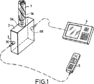
図1は本発明による無線通信装置を示す図であり、
図2は図1のシステムのアンテナの斜視図であり、
図3は導電性接地面に搭載されたアンテナの軸方向の断面図であり、
図4A、4Bおよび4Cは、異なる共振モードにおいて動作しているときの、アンテナ外面の導線の異なる定常波パターンを示すアンテナの斜視図であり、
図5はマイクロストリップダイプレクサの平面図であり、
図6Aから6Eは図5のダイプレクサの機能を示すスミスチャート図であり、
図7は単一方向スイッチを有する結合段と組み合わせた図2および図3に示されるアンテナを有する、本発明によるアンテナ方式を示す図であり、
図8は本発明による別様の無線通信装置の図であり、
図9は本発明による一体型無線通信装置の図である。
図面の図1を参照して、200MHzより上の周波数での使用のための、本発明による無線通信装置は、異なる機能を実行することができる。無線装置はアンテナ方式を組み込んでおり、アンテナ方式は第一に、外側にメッキされた金属エレメントを有する細長い円筒形セラミックロッドの形状のアンテナ1を含み、アンテナの放射エレメントとその下端の接地接続部との間に電流トラップを形成する近位導電性スリーブを有する、4本巻式ヘリカルアンテナエレメント構造を形成する。本明細書において、「放射」という用語は、送信機から適切に供給された場合にアンテナから電磁エネルギーを放射するよう作用するエレメントをさすが、受信機を含む本装置では、そのようなエネルギーを吸収しアンテナでオーム電流に変換するよう作用する。
アンテナ1は、本発明ではダイプレクサユニット3の形で結合段のケーシングの壁によって形成されている、横に延びる導電面2上に装着されている。アンテナの内部供給器構造1Aは、その共通ポート3Aにおいてダイプレクサユニット3に接続されている。無線通信機器は、ダイプレクサユニット3の第一の装置ポート3Bに接続されたGPS受信機4と、ダイプレクサユニット3の第二の装置ポート3Cに接続される携帯域電話受信機5を含む。
以下に説明されるように、アンテナ1は、間隔の離れた周波数帯域における共振の異なるモードを有する。この例では、第一の共振モードが1.575GHzの共振周波数に対応し、アンテナはその周波数で円形有極信号を最もよく獲得し、信号は全体的に垂直に、すなわちアンテナの中心軸に平行に、方向付けられる。この周波数はGPS L1周波数である。この例での第二共振モードは約860MHzの共振周波数に対応し、信号はアンテナ1の中心軸と平行の方向に線状に分極される。860MHzは携帯域電話帯域に存在する周波数の一例である。ダイプレクサユニット3は、第一および第二共振モードにおいてアンテナ1に装置4および5のインピーダンス整合を提供し、2つの装置4および5を分離して、それらが独立して、すなわち主として一方の動作が他方の動作を干渉せずに動作できるようにする。ダイプレクサユニット3については以下により詳細に説明する。
図1に示される構成は、位置決め情報および携帯域電話を介して通信する能力が共に必要とされる多数のアプリケーションに適している。この構成は特に自動車での設置に有用であり、その場合にGPS受信機4は、恒久的に装着された自動車電話または自動車の配線にプラグを差し込んだ携帯電話と同じアンテナを介してドライバーにナビゲーション情報を提供できる。アンテナ1およびダイプレクサユニット3は、小さく頑丈であり、自動車や他の移動の用途によく適している。GPS受信機と電話機を単一装置内に一緒に、必要な場合にはダイプレクサと共に組み合わせることが可能である。アンテナ1は図2および図3により詳細が示され、その開示が参照として本明細書に組み込まれる出願人による係属中の英国特許出願第9603914.4号に開示されている。その好適な形態において、アンテナは、ロッドの形をしている円筒形セラミックコアの外表面に這う金属導線として形成される4つの縦に延びるアンテナエレメント10A、10B、10Cおよび10Dを持つアンテナエレメント構造を有する4本巻式である。コア12は金属内張り16を有する軸状の通路14を有し、通路は軸状の供給器導線18を収容する。内部導線18および内張り16は、この場合、供給ラインをアンテナエレメント10A〜10Dに接続するための同軸供給器構造を形成する。また、アンテナエレメント構造は、コア12の遠端面12D上の金属トラックとして形成され、それぞれの縦に延びるエレメント10A〜10Dを供給器構造に繋げる、対応する放射状アンテナエレメント10AR、10BR、10CRおよび10DRを含む。アンテナエレメント10A〜10Dのもう一方の端はコア12の近端部を取り巻くメッキされたスリーブ20の形で共通導線に接続される。このスリーブ20は次に、コア12の近端面12P上にメッキ22により軸状路14の内張り16に接続されている。コア12の素材は、アンテナエレメント10A〜10Dおよびスリーブ20により規定される容積の主要部を占める。
コア12に好ましい素材は、ジルコニウム−チタン塩酸ベースの素材である。この素材は、上述の相対誘電率が36であり、また変化する温度に対しての寸法および電気の安定性についても留意する。誘電損は極わずかである。コアは押し出しまたは押圧により生産されてもよい。
アンテナエレメント10A〜10D、10AR〜10DRは、コア12の外側円筒面および端面に接合された金属導線トラックであり、各トラックは動作長にわたって少なくともその厚さの4倍の幅を持つ。トラックは最初にコア12の表面を金属層でメッキしてから、選択的にメッキを取り除いてコアを露出させることにより、形成されてもよい。金属層の取り除きは、プリント回路基板をエッチングするのに用いられるのと同様の、撮像層に適用されるアプローチにしたがってってエッチングすることにより行われてもよい。あるいは、参照として本出願に組み込まれる、係属中の英国特許出願第9622798.8号に開示されるように、金属素材は選択的溶着またはプリント技術により付けられてもよい。すべての場合において、寸法が不変のコアの外側に一体層としてトラックを形成することにより、アンテナが寸法が不変のアンテナエレメントを有するようになる。導線形成の別の方法は、コアの素材に溝を切り抜き、コアの外側全体をメッキし、次いで心なし研削によりメッキ被覆の外層を取り除いて、セラミック材の島を残すことを含む。
導電性スリーブ20は、同様にメッキされ、アンテナコア12の近位部を覆い、これにより、スリーブ20と軸状路14の金属内張り16との間の空間を埋めているコア12の素材で供給器構造16、18を取り巻く。スリーブ20は、図2に示すように、軸方向の平均長1Bを有する円筒を形成し、コア12の近端面12Pのメッキ層22により内張り16に接続される。第一の共振モードにおいて、スリーブ20とメッキ層22の組み合わせは、供給器構造16,18により形成された伝送線での信号を、アンテナの近位端での不安定な状態と、スリーブ20の上部接合エッジ20Uの平均の軸方向位置と同じ近位端から軸方向に離れた軸方向位置でのおおむね安定した状態との間で変換するのに効果的である。
図2からわかるように、スリーブ20は、不規則な上部接合エッジまたはリム20Uを有し、そこでピーク20Pとトラフ20Tとの間で上昇および下降する。4つの縦に延びたエレメント10A〜10Dは、長さが異なり、エレメントのうちの2つの10B、10Dは残りのエレメント10A、10Cよりも長く、これは長いエレメントがリム20Uのトラフにおいてスリーブ20と連結し、一方で残りのエレメント10A、10Cがピークに連結されるという利点によるものである。この実施形態において、第一の共振モードでの共振時に、円形有極信号の受信を意図して、縦に延びるエレメント10A〜10Cは単純な螺旋であり、それぞれはコア12の軸の周りを半回している。長いエレメント10B、10Dは短いエレメント10A、10Cよりも長いヘリカルピッチを有する。縦に延びる、対応する放射エレメントの各組(たとえば、10A、10AR)は、所定の電気的長さを有する導線を構成する。本実施形態において、短い長さを有するエレメント組10A、10ARと10C、10CRそれぞれの合計の長さが、共振の第一モードにおいて動作波長で約135°の伝送遅延に対応するよう構成されており、エレメント組10B、10BR;10D、10DRのそれぞれはほぼ225°に一致するより長い遅延を提供する。このため、平均伝送遅延は180°であり、動作波長においてλ/2の電気的長さに相当する。一般に、伝送遅延とは信号が回路を伝わる時に遅れた時間の量である。この発明では、これは位相として表現される。よって、180°の伝送遅延とは動作波長において受信した信号の半サイクル分の所用時間に相当する。長さを違えることにより、Kilgusの「Resonant Quadrifilar Helix Design」(The Microwave Journal、1970年12月、49〜54ページ)に特定される円形有極信号のための4本巻式ヘリカルアンテナに必要な移相状態が提供される。組になっているエレメントの2つ、10C、10CR;10D、10DR(すなわち、1つの長いエレメントの組と1つの短いエレメントの組)は、放射エレメント10CR、10DRの内端においてコア12の遠端の供給器構造の内部導線18に連結されている一方で、残りのエレメントの組10A、10AR;10B,10BRの放射エレメントは金属内張り16により形成される供給器スクリーンに連結されている。供給器構造の遠端において、内部導線18および供給器スクリーン16に存在する信号は、おおむね均衡しており、これにより、以下に説明するように、アンテナエレメントがおおむね均衡のとれた電源またはロードに接続されている。
縦に延びるエレメント10A〜10Dの螺旋状の通路(伝送路)の左巻きを用いて、アンテナは右巻きの円形有極信号(右円偏波信号)に最も高い利得を有する。
その代わりに、アンテナが左巻きの円形有極信号(左円偏波信号)に使用される場合、螺旋の向きは逆になり、放射エレメントの連結パターンは90°回転する。左巻きおよび右巻きの両方の円形有極信号の受信に適するアンテナの場合では、利得は少なくなるが、縦に延びるエレメントは一般に軸に平行な通路に続くよう構成される。
代替として、アンテナは上述のように異なる長さのヘリカルエレメントを有してもよいが、長さの違いはそれぞれの螺旋状中心線について、長いエレメントを曲げることにより得られる。この場合、上述された係属中の英国特許出願第2292638A号に開示されるように、導電性スリーブは一定の軸方向の長さである。
アンテナは、図3に示されるように、たとえばはんだ付けによりシート状金属板に電気的に連結されたメッキされた近端面12Pと共に、シート状金属板により提供される導電面(導電性表面)2に直接装着されることが好ましい。この実施形態において、シート状金属板は、後述するように、ダイプレクサ回路への直接の繋がりのために、ダイプレクサユニットケーシングおよびアンテナの内部導線18の一部である。アンテナコアの内部軸状路14の導電性内張り16は、アンテナの近端面12Pのメッキ層22に連結されている。
図2および図3から、アンテナは遠位端において電流給電されることが理解されよう。第一の共振モードにおいて、スリーブ20はトラップエレメントとして動作し、主としてアンテナエレメント10A〜10Dを地面から分離する。図4Aに示されるように、エレメント10A〜10D中の定常波電流の振幅は、スリーブ20のリム20Uにおいて最大であり、ここでは2組のエレメント10A、10Cおよび10B、10Dがアンテナの接地した近端面12Pから分離されている2つのループの部分を形成するよう、リムで順に巡る。定常波電流の最小はおおよそエレメント10A〜10Dの真中に存在する。最大電圧Hおよび最小電圧Lはそれぞれ電流が最小および電流が最大になる場所で起こる。この共振モードで、図2に示されるアンテナは、上述されたように、右巻きの円形極性をもつ信号(右円偏波信号)を受信するのに適した左巻きの螺旋状伝送路を備えている。このアンテナ配置は左巻きの円形極性をもつ信号(左円偏波信号)を受信するのには適しておらず、ゆえに左巻きの円形極性を弁別する。
この実施形態において、共振の第二モードは、より低い周波数においてであり、図4Bに示されるように、共振の第一モードとはかなり異なるモードで表す。再び、アンテナは頂部で電流給電されるが、スリーブのリム20Uにおいて、またはその近傍において(特には、リム20Uのわずか上の領域であり、この領域は遠位供給点および近位供給点の間のおおよそ中間である)、アンテナエレメント10A〜10D中で定常波電流は最小に下がり、電圧は最大になる。最大電流および最小電圧(L)は、両極、すなわち遠位供給点および近位接地接続部において発生する。電流はスリーブ20の表面で比較的高いが、そこでは電流はアンテナの放射パターンに影響を与えない。アンテナは、大部分が単一端の供給を有する従来の逆のモノポールに非常に類似する方法で、1/4波長共振を示す。リム20Uの周辺にはほとんど電流の流れがなく、これは単一端供給に一貫している。このモードでは、アンテナは、コアの中心軸に平行して線形極性信号(垂直偏波信号)と共に、モノポールアンテナの古典的な円環型パターンを示す。水平極性に対しての強い信号弁別(discrimination)がある。
図4Cに示されるように、アンテナ1はまた第三共振モードを有する。これは、より高い周波数の単一端モードであり、アンテナは動作波長において約180°の電気的長さを有する代わりに、約360°(すなわち、遠位供給点からスリーブの接地接続部まで)の電気的長さを有する。共振の周波数は、第二共振モードの約2倍である。第二モードでのように、定常波パターンは両極で最大電流と最小電圧を示すが、この場合では、図4Cに示すように、最小電圧Lがまた極間および2つの最大電圧Hの中間位置間の電気的な中間にある。図1の無線通信装置は、第三共振モードを利用しないが、結合段の適切な変形により、共振の適切な周波数において回路で動作可能な接続が可能になる。
記載および図示されている装置は、1575MHzおよび800〜900MHzの携帯域電話帯域での使用を意図したものであるが、1700〜1800MHzPCN携帯域電話帯域で付加的に動作する代わりの構成が可能である。アンテナまたはそれに類似するものは、高および低携帯域電話帯域、すなわち800〜900MHzおよび1700〜1800MHz、またはGPS周波数および高携帯域電話帯域のみ、で単独で使用されてもよい。もちろん、他の組み合わせも可能であり、アンテナ部品はそれに応じて変更される。しかし、一般的に、共振の複数の単一端モードは、遠位供給器接続部とトラップまたはスリーブの接地接続部との間の導電性部品の電気的長さが、それぞれの共振周波数において、n×180°に等しい場合において可能である。ただし、nは整数、すなわち1,2,3,....である。上述された2つの単一端モードでは、それぞれn=1および2である。これらの各モードは、トラップまたはスリーブの繋ぎ目での最大電流および供給器構造によって、すなわちトラップまたはスリーブの接地接続部においてまた互いに空間的に相にある各組の正反対のヘリカルエレメントでの電流によって、特徴づけられる。反対に、均衡のとれたモードでは、そのような電流は反対相、すなわち等しい電流が反対方向に流れている。
同様に、均衡のとれたモードを第一の共振モードよりも高い周波数で行うことが可能であり、そのモードでは、遠位供給接続部とトラップ、特にスリーブのリム、の間の平均電気的長さは約m×180°であり、ここではm=1,2,3,...である。
アンテナが1.575GHzでGPS信号を、および800〜900MHzの領域での携帯域電話信号を受信できるため、コア12の長さおよび直径は、一般的にそれぞれ20から35mmおよび3から7mmの領域にあり、スリーブ20の平均軸方向の範囲は8mmから16mmの領域にある。図2および図3に示される特に好適なアンテナは、約28.25mmのコア長、および約5mmの直径を有し、スリーブ20の平均軸方向の長さは約12mmである。共振の4本巻式モードの1つの驚くべき特徴は、このモードでの性能が、それぞれの共振周波数において90°の伝送遅延に対応するものからのスリーブ20の平均軸方向長さでのいくらかの変形に、この長さが共振の第二モードにおいて必要とされる共振周波数を得るよう調節できる程度まで、耐えることである。しかしながら、スリーブ20の軸方向の長さを1/4波長からさらに変化させることが求められ、4本巻式モードでのアンテナの性能が許容できない程度まで損なわれる場合には、直列のチョークをスリーブ20とダイプレクサユニット2(特に、アンテナに隣接する導電性表面(図1参照))の間に挿入して、アンテナ遠位面12Dにおいて少なくともおおまかにバランスのとれた電流ドライブを取り戻すことが可能である。
上記の寸法を決定するのに用いられる設計プロセスにおいて、おおよその推定概算は、幾何学的形状が伝送線としてのモデル化を容易にするような領域とは対照的に、アンテナのフリンジング(fringing)またはわずかなフィールドが発生する領域を、無視している。このため、フリンジングパスを、遠位放射エレメント10ARから10DR、スリーブ20のリム20Uおよび近位面22により提供されるものとして見てもよい(図2および図3参照)。ヘリカルエレメント10A〜10D中の電流は、漏電性ガイド伝播になるとみなしてもよく、一方、スリーブ20で縦に発生するものは、スリーブを形成する導電層の内表面で発生し、非漏電性ガイド伝播を生成する。
したがって、たとえば、アンテナエレメントにより形成されるラインのガイドパラメータεeffは、様々なヘリカルラインピッチを表すことができる。各ヘリカルラインは、軸方向の伝播を意図し、コアの相対誘電率εfおよびそのコアとエレメント構成に依存する、相対誘電率εeffの誘電媒体によって囲まれている伝送線とみなすことができる。このパラメータεeffはライン中の相速度と軸方向に分解されるεeffの値を順番に割り出す固有値の遅延測定を行うことによって測定される。たとえば、εeffがピッチ角度に対してプロットされ、5mmのコア直径と様々なヘリカルピッチの測定を行って、中間のピッチ角度でのεeffの概算を可能にするグラフを作り出すことが可能である。
したがって、特性ラインパラメータは、それぞれの対となっているヘリカルエレメントの寸法が安定した動作に必要な共振周波数(上記第一の共振モード)での相において必要とされる電気的長さの合計λ、すなわち360°におおよそ対応するように規定されているアンテナを構築するために使用することができる。実際に、最もよい円形極性の利得を達成するために1つの組は求められる共振周波数より若干高い周波数で360°に等しく、もう1つの組は若干低い周波数で360°に等しくなるべきである。
このように、ヘリカルエレメントの長さを計算し、第二の共振モードで要求される共振周波数でのこれらの要素の電気的長さは、単純に、2つの共振モードのそれぞれの周波数の比率による調整と、全体のモノポール電気的長さ180°からその調整された長さを引き、スリーブに必要とされる電気的長さを割り出すことによって算出される。この場合、図4Bに示されている第二の共振モードに対応し、第一モードよりも低い周波数で単一端動作が求められている場合には、180°を選択する。こうして、第二の共振モードに対して必要な低周波数を知ることにより、スリーブの長さを概算することが可能となる。
その代わりとして、単一端動作に対する周波数が必要な場合、図4Cに示される第三共振モードが用いられるため、ヘリカルエレメントとスリーブの電気的長さの合計として360°が選択される。
無線通信回路へのアンテナの接続では、図1のダイプレクサユニット3が一組のフィルタと、リアクタンス補償スタブ、およびアンテナを装置4、5の両方に合わせ、片方の信号をもう一方の信号から分離させるインピーダンス変圧エレメントを収容する。
別の配置としては、図8によって示され、以下に述べられているように、アンテナはダイプレクサユニットから離して取り付けることができる。
図5に示されているように、図1のダイプレクサユニット3には、一方に導電接地層、もう片方には図示されているような導線を有する絶縁板30(絶縁板30の見えない側面は図5に示されている)を取り囲むしきりがある。これらの絶縁体は第一に、一方の終端33がアンテナ内部導線に通じ、もう一方の終端34が回路ノードである伝送線部を形成する導電板としてのインピーダンス変圧部32である。第二に、ノード34に連結されているのは、バンドパスフィルタ36,38である。それぞれは、誘導的に連結された3つの平行共振エレメントにより構成されており、各エレメントは、メッキ通し穴36B、38Bにより一端で接地された狭い誘導ストリップ26A、38Aで作られ、反対の端に、コンデンサ板36C、38Cを有しており、コンデンサ板36C、38Cは基板のもう一方の端に接地線を有するコンデンサを形成している。各フィルタ36、38の場合、ノード34に最も近接する誘導ストリップ36A、38Aは、先細になり、さらなるインピーダンス変圧をもたらす電気的に短いタッピング導線40によりノード34に連結されている。それぞれの場合において、ノード34から最も離れた誘導ストリップは、(フィルタ近くで先細になる)タッピングライン42に繋がっており、フィルタをそれぞれの機器接続44に連結している。
フィルタ36,38の異なるサイズから明白なように、それらは異なる周波数帯域、実際には、アンテナ1の2つの共振モードに対応する2つの帯域、になる。
両方の共振周波数でのインピーダンス整合は、変圧部32および、図5に示されるように、ノード34から延びる開路エンドスタブ46との組み合わせにより、達成される。
変圧部32は、
Z0=√(ZSZL)
により与えられる特性伝送線インピーダンスZ0を有するよう大きさが決められる。ただし、ZSは共振でのアンテナ1の特性インピーダンスであり、ZLはフィルタ36および38に適合するように選択されたノード34の負荷インピーダンスである。変圧部32の長さは、第一および第二の共振モードに対応する2つの周波数帯域間のおおよそ中間の周波数、この場合では約1.22GHz、での約90°の伝送遅延に対応するよう構成される。異なる周波数での変圧部32の効果は、図6Aのスミスチャートに示されており、これは変圧部32に0.1から1.6GHzまでの周波数の範囲にわたってスタブ46がないために、ノード34において見られるインピーダンスを表す。曲線のAおよびB部は中心が860MHzおよび1.575GHzにある2つの周波数帯域を示し、抵抗性インピーダンスがチャートの中心、上述のように、2つの帯域間の周波数で、得られることがわかるであろう。スタブ46(図5参照)の効果が、図6Bのスミスチャートを参照して考慮される。低周波数において、ノード34でスタブ46のみにより提示されるインピーダンスは、図6Bにおけるカーブ端がチャートの右側に近くなっていることから明白なように、比較的高い。周波数が増加するにつれて、スタブ46の選択された長さのために、周波数帯域AおよびBの間のおおよそ中間の周波数に対応する0インピーダンスポイントを通じて、インピーダンスはチャートの周辺で順に回る。
図6Aと図6Bを比較すると、ノード34におけるインピーダンスは、帯域Aにある変圧部32のために誘導性リアクタンス成分を有し、帯域Bにおけるインピーダンスは容量性リアクタンス成分を有することに気が付くであろう。スミスチャートでは、右の端から出た曲線は、定リアクタンスの線である。図6Bから、スタブ46は、帯域Aのノード34においてスタブ46によって単独で提示されるインピーダンスのリアクタンス成分が容量式であり、図6Aに示される帯域Aにおける誘導性リアクタンスと少なくとも略等しいような寸法であることがわかるであろう。同様に、帯域Bにおいてスタブ46に起因するインピーダンスは、図6Aに示されるように帯域Bにおける容量性リアクタンス成分と大きさが少なくとも略等しい誘導性リアクタンス成分を有する。
次に図6Cを参照して、ノード34におけるインピーダンスのトレースは、変圧部32とスタブ46との組み合わせにより、図1に示されたポート3Aにおける電源インピーダンスと対応するインピーダンスにおいて低周波数で始まるループに追従する。このトレースは、周波数の上昇とともに、抵抗線を2回交差するループに追従する。最初の交差は、図6Dにおいて曲線で示されるように、図6Cにおいて示された周波数帯域Aに相当する曲線の単なる一部である帯域Aの略中心に相当しており、抵抗線の二度目の交差は、図6Eにおいて曲線で示されるように、同様に図6Cに図示された曲線の一部である帯域Bの略中心を表す。このように、ダイプレクサのエレメントは、周波数帯域AとBのどちらにおいてもフィルタ36、38に対するアンテナ1のインピーダンス整合を良好に行い、スタブ46のリアクタンスは変圧部に起因するリアクタンスの少なくとも一部を補償している。それぞれのフィルタは、他のフィルタの周波数において比較的高いインピーダンスを呈しているため、2つの帯域において信号間に分離(isolation)をもたらす。
図1に示される例では、この分離を使用して、GPS受信機4を、電話機5におよび電話機5から供給される携帯電話信号から分離する。
ダイプレクサ3は、無線通信機4および5(図1参照)を同時に動作すべき場合に適する。本発明が適用可能である場合、同時動作は要求されず、図7に示されるようにR.F.スイッチを含む結合段がより適当である。アンテナ1の近端部の供給器構造は、共通信号線またはポート47Aを通って、インピーダンス整合セクション48を介して二方向R.F.スイッチ49に結合されており、これが典型的なP.I.N.ダイオード装置である。スイッチ49の状態に応じて、共通線47Aは、2つのまた別の信号線またはポート47B、47Cの一方または他方に結合され、これらに別の通信回路ユニットが接続される場合がある。
インピーダンス整合セクション48の性質は、適合されるべき周波数に基づく。密な周波数で動作するユニットと併用してアンテナ1を使用することを目的としたシステム等、場合によって、図5のダイプレクサにおけるセクション32のように90°の単純な伝送線変圧器で充分であることもある。かかるシステムの例は、PCN携帯電話の動作(1710〜1785MHzおよび1805〜1880MHz)とDECTワイヤレス自局ループ電話の動作(1880〜1900MHz)とを組み合わせたものである。または、周波数帯域がより広い間隔である場合、2つのピークを持つインピーダンス整合の構造、たとえば図5のダイプレクサの変圧器32とスタブ46のように90°の変圧器と開回路のスタブの組み合わせを使用してもよい。この場合、スイッチ49は、変圧器とスタブの繋ぎ目に接続される。
別様のアンテナ方式が図8に示されている。この場合、アンテナ1は、ダイプレクサのケーシングの一部であるよりむしろ、車体等別の金属構造の一部を形成する横方向に延びた導電性の面2に装着されている。アンテナは、図1を参照して上記記載の実施形態のダイプレクサと類似するダイプレクサ3の共通ポート3Aと結合された供給ケーブル50によって、表面2の孔を通して結合されている。供給ケーブル50は、内部の導線がアンテナ1の軸状の内部導線と結合され、外側のシールドがアンテナのメッキされた近位面に接続されている。ケーブル50のダイプレクサ側端部では、該シールドがダイプレクサのケーシングと接続されており、ケーシング内にあるマイクロストリップダイプレクサボードの接地面と直接または間接的に接続されている。これは、図4に示されているものと同様である。
供給ケーブル50の特性インピーダンスがアンテナ1によって表される電源インピーダンスと同一でない限り、ケーブル50は、インピーダンス変圧エレメントとして作用する。これが発生する程度は、ケーブル長と特性インピーダンス値に依存しており、また、マイクロストリップダイプレクサエレメントは、アンテナ1とダイプレクサのノード34との間に発生する所要の総インピーダンス変圧(図4参照)が、上記第1実施形態、さらに図1および図4に示されるダイプレクサの変圧部32と同一の効果を有するように、これに応じて変えられる。したがって、ケーブル50とダイプレクサ3のインピーダンス変圧部の結合の電気的長さは、第1および第2の共振モードと対応する2つの周波数帯域間の略中間の周波数において約90°である。したがって、マイクロストリップダイプレクサは、図4に示されるように、ただしインピーダンス変圧部32がかなり減退された長さであり、または負荷34における負荷インピーダンスと等価の特性インピーダンスを有するマイクロストリップ部によって少なくとも一部を形成されることが可能である。典型的には、供給ケーブル50は、10オームの特性インピーダンスを有する。
図8のシステムは、上記記載の別様のアンテナを使用しており、略同延かつ同軸の4個のヘリカルエレメントを有しながら、正反対に配置された2個のエレメントが曲折する経路をたどって異なる長さとなり、円形有極信号に4本巻式ヘリカルアンテナに要求される移相状態を引き起こす。1組のエレメントの曲折は、図2に示されるスリーブ20の不規則なリムの位置を取っており、このため、本実施形態では、スリーブ20は、円形状の上縁部が近端部から一定間隔でアンテナコアを中心として延設されている。曲折エレメントに対するガイドパラメータの特徴づけは、上記略述するように、同一の平均ピッチ角を有する単純な螺旋について求められた∈offのかけ算器として伸長因数(extension factor)によって達成できる。
上記の実施形態では、アンテナ1とその結合段は、別個の無線通信装置に接続されて図示されている。本発明は、図9に示されるような一体型装置に適用可能であることが理解されよう。この例では、単体のハンドヘルド型ユニットは、GPSおよび携帯電話回路の両方、詳細には、GPS受信機4’および電話送受信機5’を内蔵している。これらは、ダイプレクサ2’およびアンテナ1とともに、すべて単体のケーシング60に収納されている。The present invention relates to an antenna with an elongated dielectric core, an elongated conductive element on or adjacent to the outer surface of the distal end of the core, and a conductive trap such as a conductive sleeve surrounding the proximal end of the core. It is related with the radio | wireless communication apparatus containing. The present invention also relates to an antenna system including the antenna and a novel use of the antenna.
The antenna described above is disclosed in a pending UK patent application previously published in the applicant by the same applicant in US Pat. No. 2,292,638A, the subject matter of which is incorporated herein by reference. In its preferred form, the antenna of the application has a cylindrical ceramic core, the volume of the solid ceramic material of the core accounting for at least 50% of the envelope inner product defined by the elongated conductive elements and the sleeve. And the element is on the cylindrical outer surface of the core.
The antenna, in particular, receives a circular polarized signal (circularly polarized signal) from a power source that can penetrate the antenna, just above the antenna, ie at several degrees above its axis or above the plane orthogonal to the antenna axis. Or from a power source located anywhere in the solid angle between both ends. Such signals include signals transmitted by satellites of satellite navigation systems such as GPS (Global Positioning System). In order to receive such a signal, the elongated conductive element includes four co-extensive helical elements having a common central axis that is the axis of the core, the element comprising one set of elements and another set of elements. It is formed as two sets of elements having a longer electrical length and facing in the lateral direction.
Such an antenna has advantages over a firm and small air-core antenna and a patch antenna having a gain that is relatively equal to the solid angle where the transmission satellite source is located.
The Applicant has discovered that such antennas can be used in different frequency bands spaced from each other. Accordingly, the present invention provides a wireless communication apparatus including an antenna and wireless communication circuit means connected to the antenna and operable in at least two radio frequency bands. Wherein the antenna is disposed at or adjacent to an elongated dielectric core, a feeder structure extending substantially through the core from one end of the core to the other, and the outer surface of the core; Including an elongated conductive antenna element and at least one series combination of conductive trap elements connected in ground to the feeder structure in the region of the one end of the core. In addition, the antenna element or each antenna element is coupled to a supply connection of a feeder structure in the region of the other end of the core. Further, the wireless communication circuit means includes two parts operable in the first and second radio frequency bands, each flowing between the common signal line of the antenna feeder structure and each circuit means part. Corresponding to each signal line of the carrier signal, the antenna resonates in the first resonance mode in the first frequency band and in the second resonance mode in the second frequency band.
For example, if the trap substantially isolates the elongated conductive element from the ground connection at the near end of the antenna, the first resonant mode corresponds to a supply current that is substantially balanced at the far end of the supply structure. May be. In the case of a trap in the form of a conductive sleeve surrounding an antenna and a dielectric rod with one or more sets of elongated conductive elements acting as radiating elements, that or each set of elongated conductive elements acts as a loop, Flows along the rim of the sleeve between the set of opposing elements. In the case of an antenna in which two or more sets of helical elements form loops with different electrical lengths, such balanced operation is typically directed to a solid angle about the common central axis of the helical elements. Corresponds to the attached circular polarized signal. In this first mode, the antenna represents the maximum current or minimum voltage near or at the connection between the feeder structure and the elongated conductive element, or near or at the connection to the sleeve rim. There is a case.
The second resonant mode preferably corresponds to a single-ended or unbalanced supply current at the far end of the feeder structure, which is typically a linearly polarized signal, especially the center of the antenna. This is a case where the antenna resonates in a unipolar mode for transmitting and receiving signals polarized in the axial direction. Such a resonant mode is characterized by a standing wave minimum current substantially midway between the ends of the rod.
In the first resonant mode, the resonant frequency is typically a function of the electrical length of the elongated element, and the resonant frequency of the second resonant mode is (a) the electrical length of the elongated element and (b) the sleeve. Is a function of the sum of the electrical lengths of In the general case, the electrical length of the elongated conductive element produces an average transmission delay of at least approximately 180 °, for example, at a resonant frequency corresponding to the first resonant mode. The frequency of the second resonance mode is determined by the sum of the electrical length average of the elongated conductive elements in the longitudinal direction and the electrical length average of the sleeve corresponding to a transmission delay of at least about 180 ° at that frequency. May be.
The present invention further includes an antenna scheme for radio signals in at least two frequency bands. The antenna system includes an elongated solid dielectric core, at least one elongated conductive element at or adjacent to the outer surface of the distal end of the core, and a longitudinal feeder structure extending through the core An elongated conductive element extending between a distal connection with a feeder structure and a distal rim of the sleeve, the sleeve coupled proximally with the feeder structure Antenna, a common signal line corresponding to the feeder structure, at least two other signal lines for connecting to a radio signal processing device operating in the frequency band, and the feeder structure and the other A coupling stage having an impedance matching section and a signal directing section connected between the signal lines, the signal directing section being connected to the common signal line and one of the bands The antenna is coupled together with one of the two other signal lines for a signal that resonates in the first resonance mode, and is on the other of the bands with the common signal line, A coupling stage configured to couple together the other of the two separate signal lines for a signal that resonates in a second resonance mode.
In a preferred embodiment of the antenna scheme, the coupling stage is a diplexer having a filter coupled between a common signal line and the other signal line, the filter being one of the two other signal lines. A first filter that is tuned to a high frequency in one of the two frequency bands, and corresponds to the other of the two other signal lines, and out of the two frequency bands. And a second filter tuned to a low frequency on the other side. The diplexer includes an impedance transformer element coupled between the common signal line and a node to which the filter and the impedance compensation stub are connected. Transformer elements, filters and stubs are conveniently formed as microstrip components. In such a structure, the transformer element may include a conductive strip on an insulating substrate whose opposite surface is coated with a conductive ground layer. The strip forms a transmission line with a predetermined characteristic impedance in cooperation with the ground layer. Similarly, the stub may be formed as a conductive strip having an open circuit end. The filter may be formed of a microstrip element that is on the same substrate as the transformer element and the stub. These filters are preferably connected to the nodes by electrical leads that are electrically short compared to the electrical length of the transformer element.
The transformer element may include a cable length connected in series between the antenna feeder structure and the diplexer node, or the characteristic impedance of the power source impedance constituted by the antenna and the load impedance selected for the node. It may include a series combination of the cable in between and the microstrip length between the feeder structure and the node.
The use of a diplexer provides simultaneous operation of the wireless communication device in both frequency bands. If simultaneous operation is not required, the coupling stage may be of a simpler structure, as a signal directing section, between the common signal line and the one other signal line, or between the common signal line and the other another. It includes a switch for routing a signal between any of the signal lines.
Antenna schemes typically operate only in two frequency bands, but within the scope of the present invention, it is possible to provide schemes that operate in more than two spaced bands, There are as many resonance modes as possible.
According to a third aspect of the invention, there is provided an antenna system as described above, a satellite positioning or timing receiver connected to one of the other signal lines of the coupling stage (eg a GPS receiver), and A wireless communication system is provided that includes a portable or mobile telephone connected to another one of the other signal lines of the stage. When the coupling stage is a diplexer, the antenna and the filter are configured such that the resonant frequencies corresponding to the different resonant modes of the antenna are in the receiver operating band and the telephone operating band, respectively.
As will be described later, the diplexer is a diplexer that operates at a frequency higher than 200 MHz, and includes an antenna port, an impedance transformer in the shape of a transmission line having one end coupled to the antenna port and the other end forming a circuit node. , First and second device ports, tuned to one frequency, connected to the first device port between the node and the first device port, and tuned to another frequency, the node A second bandpass filter connected between the second device port and a reactance compensation element, such as an open circuit stub element, connected to the node to compensate for at least partial reactance of the transmission line; including.
If the coupling stage has a switching device as the signal directing section, the impedance matching section may be similarly formed as an impedance transformer and reactance compensation element in the form of a transmission line, the switching device being between these two Connected to the node.
The transmission line length forming the impedance transformer may be adapted to perform a resistive impedance transformation at a frequency between high and low frequencies so that the impedance at the node is transformed at the two frequencies. The capacitor has a capacitive reactance component and an inductive reactance component, respectively, and the stub length causes inductive and capacitive reactance at the two frequencies, respectively, so that it is slightly more resistant than the impedance due to the transmission line. The transformer compensates at least in part for capacitive reactance and inductive reactance to provide the node with the impedance obtained at each of the two frequencies.
Typically, the transmission line length is one that provides a transmission delay of about 90 ° at a frequency that is at least about halfway between the high and low frequencies.
According to a fourth aspect of the present invention, there is provided an elongated derivative core having a relative dielectric constant of 5 or more and a longitudinally extending and laterally extending at or adjacent to the outer surface of the distal end of the core. At least one set of elongated conductive elements arranged in diametrically opposed relationship, a conductive sleeve surrounding the proximal end of the core, and a longitudinal feeder structure extending through the core; The elongated conductive element provides a new use of an antenna that extends between a distal connection to the feeder structure and a distal rim of the sleeve, the new use being one of the bands The antenna contains a frequency exhibiting a first resonance mode, and another one of the bands contains a frequency where the antenna exhibits a second resonance mode different from the first mode, and in a different part of the radio signal processing device Or part from said feeder Through the granulation of the common signal line, each consists of operating the antenna in two frequency bands spaced at least interval for supplying a signal operating at different respective one of said band.
The invention will be described in the following with reference to the drawings.
FIG. 1 shows a wireless communication apparatus according to the present invention.
2 is a perspective view of the antenna of the system of FIG.
FIG. 3 is an axial sectional view of an antenna mounted on a conductive ground plane,
4A, 4B and 4C are perspective views of the antenna showing different standing wave patterns of conductors on the outer surface of the antenna when operating in different resonance modes;
FIG. 5 is a plan view of a microstrip diplexer,
6A to 6E are Smith charts showing functions of the diplexer of FIG.
FIG. 7 shows an antenna scheme according to the invention with the antenna shown in FIGS. 2 and 3 combined with a coupling stage having a unidirectional switch;
FIG. 8 is a diagram of another wireless communication device according to the present invention,
FIG. 9 is a diagram of an integrated wireless communication apparatus according to the present invention.
Referring to FIG. 1 of the drawings, a wireless communication device according to the present invention for use at frequencies above 200 MHz can perform different functions. The wireless device incorporates an antenna system, which first includes an
The
As will be described below, the
The configuration shown in FIG. 1 is suitable for many applications where both positioning information and the ability to communicate via a cellular phone are required. This configuration is particularly useful for installation in automobiles, in which case the GPS receiver 4 navigates to the driver via the same antenna as a permanently installed car phone or a mobile phone plugged into the car wiring. Can provide information. The
A preferred material for the
The
The
As can be seen from FIG. 2, the
Using the left-handed spiral path (transmission path) of the
Instead, when the antenna is used for a left-handed circular polarized signal (left-hand circularly polarized signal), the direction of the spiral is reversed and the coupling pattern of the radiating elements is rotated 90 °. In the case of an antenna suitable for receiving both left-handed and right-handed circular polarized signals, the gain is reduced, but the longitudinally extending elements are generally configured to follow a path parallel to the axis.
Alternatively, the antenna may have helical elements of different lengths as described above, but the difference in length is obtained by bending the long elements for each helical centerline. In this case, the conductive sleeve is of a certain axial length, as disclosed in the above-mentioned pending UK patent application No. 2292638A.
As shown in FIG. 3, the antenna has a conductive surface (conductive surface) provided by the sheet metal plate together with a plated near
2 and 3, it can be seen that the antenna is current fed at the distal end. In the first resonance mode, the
In this embodiment, the second mode of resonance is at a lower frequency and is represented by a mode that is significantly different from the first mode of resonance, as shown in FIG. 4B. Again, the antenna is galvanized at the top, but at or near the
As shown in FIG. 4C, the
The device described and illustrated is intended for use in the 1575 MHz and 800-900 MHz cellular telephone bands, but alternative configurations are possible that additionally operate in the 1700-1800 MHz PCN cellular telephone band. . The antenna or the like may be used alone in the high and low mobile phone bands, ie 800-900 MHz and 1700-1800 MHz, or only the GPS frequency and the high mobile phone band. Of course, other combinations are possible and the antenna components are changed accordingly. However, in general, multiple single-ended modes of resonance indicate that the electrical length of the conductive component between the distal feeder connection and the ground connection of the trap or sleeve is n at the respective resonance frequency. It is possible in the case equal to x180 °. Where n is an integer,
Similarly, a balanced mode can be performed at a higher frequency than the first resonant mode, in which the average electrical length between the distal supply connection and the trap, in particular the rim of the sleeve. Is about m × 180 °, where m = 1, 2, 3,. . . It is.
Because the antenna can receive GPS signals at 1.575 GHz and mobile phone signals in the 800-900 MHz region, the length and diameter of the
In the design process used to determine the above dimensions, an approximate estimate is that the fringing of the antenna, as opposed to the region where the geometry facilitates modeling as a transmission line. ) Or areas where a few fields occur are ignored. For this reason, the fringing path may be viewed as provided by the distal radiating elements 10AR to 10DR, the
Thus, for example, the guide parameter ε of the line formed by the antenna element eff Can represent various helical line pitches. Each helical line is intended for axial propagation and has a relative dielectric constant ε of the core f And relative permittivity ε, depending on the core and element configuration eff It can be regarded as a transmission line surrounded by a dielectric medium. This parameter ε eff Is the phase velocity in the line and is resolved axially ε eff Is measured by performing a delay measurement of eigenvalues that sequentially determine the values of. For example, ε eff Is plotted against the pitch angle, with 5 mm core diameter and various helical pitch measurements, eff It is possible to create a graph that allows an approximation of
Therefore, the characteristic line parameter is the sum of the electrical lengths λ required in the phase at the resonance frequency (first resonance mode) required for stable operation of each pair of helical elements. That is, it can be used to construct an antenna that is defined to roughly correspond to 360 °. Indeed, in order to achieve the best circular polarity gain, one set should be equal to 360 ° at a frequency slightly higher than the desired resonant frequency and the other should be equal to 360 ° at a slightly lower frequency.
In this way, the length of the helical element is calculated and the electrical length of these elements at the resonance frequency required in the second resonance mode is simply due to the ratio of the respective frequencies of the two resonance modes. Calculated by subtracting the adjusted length from the total monopole electrical length of 180 ° and determining the electrical length required for the sleeve. In this case, 180 ° is selected when a single-end operation is required at a frequency lower than that of the first mode, corresponding to the second resonance mode shown in FIG. 4B. Thus, knowing the low frequency required for the second resonant mode makes it possible to approximate the length of the sleeve.
Instead, if a frequency for single-ended operation is required, the third resonance mode shown in FIG. 4C is used, so 360 ° is selected as the total electrical length of the helical element and sleeve.
In connecting an antenna to a wireless communication circuit, the
In another arrangement, as shown by FIG. 8 and described below, the antenna can be mounted away from the diplexer unit.
As shown in FIG. 5, the
As is apparent from the different sizes of the
Impedance matching at both resonant frequencies is achieved by a combination of
The
Z 0 = √ (Z S Z L )
Characteristic transmission line impedance Z given by 0 Is sized to have However, Z S Is the characteristic impedance of the
Comparing FIG. 6A and FIG. 6B, it will be noted that the impedance at
Referring now to FIG. 6C, the impedance trace at
In the example shown in FIG. 1, this separation is used to separate the GPS receiver 4 from the mobile phone signal supplied to and from the
The
The nature of the
Another antenna scheme is shown in FIG. In this case, rather than being part of the diplexer casing, the
As long as the characteristic impedance of the
The system of FIG. 8 uses another antenna as described above, and has four helical elements that are substantially coextensive and coaxial, but follows a path in which two elements arranged in opposite directions bend. Therefore, the circularly polarized signal causes a phase shift state required for a four-turn helical antenna. The bending of the set of elements takes the position of the irregular rim of the
In the above embodiment, the
Claims (14)
前記アンテナは、細長い誘電体コアと、実質的に該コアの一端から他端まで該コアを貫通する供給器構造と、該コアの外側表面にまたはこれに隣接して配置され、該コアの前記一端の領域において前記供給器構造と接地接続した、細長い導電性アンテナエレメントと導電性トラップエレメントとの少なくとも1つの直列結合とを含み、該アンテナエレメントまたはそれぞれのアンテナエレメントは該コアの前記他端の領域において前記供給器構造の供給接続と結合され、
前記無線通信回路手段は、第1および第2の無線周波数帯域においてそれぞれ動作可能な2つの部分を備え、それぞれは、前記供給器構造の共通信号線と各回路手段部分との間を流れる搬送信号の各信号線とそれぞれ対応しており、
前記アンテナは、前記第1周波数帯域において第1の共振モードで、前記第2周波数帯域において第2の共振モードで共振する無線通信装置。An antenna, and wireless communication circuit means connected to the antenna and operable in at least two radio frequency bands,
The antenna is disposed in an elongated dielectric core, a feeder structure extending substantially through the core from one end of the core to the other end, and at or adjacent to the outer surface of the core. in the region of one end grounded connected to the feeder structure, and at least one series combination of the elongated conductive antenna element and the conductive trap element, the antenna element or each antenna element of said other end of the core Combined with the supply connection of the feeder structure in the region,
The wireless communication circuitry means includes an operable two parts respectively in the first and second radio frequency bands, respectively, conveying signals flowing between the common signal line and the respective circuit means part of the feeder structure Correspond to each signal line of
The antenna is a wireless communication device that resonates in a first resonance mode in the first frequency band and in a second resonance mode in the second frequency band.
前記アンテナを別個の共振部に分割する塊状のフィルタ成分を具備することなく形成され、前記一体型構造のすべての伝導経路は、あらゆる周波数の電流に利用可能であり、各共振周波数における共振経路はその周波数において好適な経路である、
請求の範囲第1項または第2項に記載の装置。The series-coupled conductive element and the dielectric core constitute an integrated structure having a plurality of different resonance modes, and the resonance modes are maximum and minimum standing waves of different patterns in the integrated structure;
Formed without a bulky filter component that divides the antenna into separate resonating parts, all the conduction paths of the unitary structure can be used for currents of all frequencies, and the resonance paths at each resonance frequency are A preferred path at that frequency,
Apparatus according to claim 1 or claim 2.
細長い立体型誘電体コア、該コアの遠端部の外側表面にまたはこれに隣接して配置された少なくとも1つの細長い導電性アンテナエレメント、および該コアを通って延設する縦方向の供給器構造を有するアンテナであって、前記細長い導電性アンテナエレメントは、前記供給器構造との遠位接続部とスリーブの遠位リムとの間に延設し、該スリーブは、該供給器構造と近位に結合されているアンテナと、
該供給器構造と対応する共通信号線、前記周波数帯域において動作する無線信号処理装置と接続するための少なくとも2個の別の信号線、および該供給器構造と該別の信号線との間に接続されたインピーダンス整合セクションならびに信号方向付けセクションを有する結合段であって、該信号方向付けセクションは、前記共通信号線と、該帯域のうちの一方にあり、前記アンテナが第1の共振モードにおいて共振する信号のための該2つの別の信号線のうちの一方とを共に結合し、かつ前記共通信号線と、該帯域のうちの他方にあり、前記アンテナが第2の共振モードにおいて共振する信号のための該2つの別の信号線のうちの他方とを共に結合するように構成される結合段と、
を含むアンテナ方式。In an antenna scheme for radio signals in at least two frequency bands,
An elongated solid dielectric core, at least one elongated conductive antenna element disposed on or adjacent to the outer surface of the distal end of the core, and a longitudinal feeder structure extending through the core an antenna having the elongated conductive antenna element and extends between the distal rim of the distal connecting portion and the sleeve with the feeder structure, the sleeve, said feeder structure and proximal An antenna coupled to the
A common signal line corresponding to the feeder structure, at least two other signal lines for connecting to a radio signal processing device operating in the frequency band, and between the feeder structure and the other signal line A coupling stage having a connected impedance matching section as well as a signal directing section, the signal directing section being on one of the common signal line and the band, wherein the antenna is in a first resonant mode while a were combined together in one of the two further signal lines for resonance signal, and said common signal line, located on the other of the band-, the antenna resonates at the second resonance mode A coupling stage configured to couple together the other of the two separate signal lines for a signal;
Including antenna system.
前記高周波数は、該細長いエレメントの電気的長さの関数であり、前記低周波数は、該細長いエレメントの電気的長さと該スリーブの電気的長さの和の関数であり、
前記細長い導電性エレメントの電気的長さ平均は、前記高周波数において180°または略180°であり、前記アンテナの縦方向にある該細長い導電性エレメントの電気的長さの平均と該スリーブの電気的長さの平均の和は、前記低周波数において180°または略180°である、請求の範囲第8項に記載のアンテナ方式。The first resonant mode is a maximum current at the connection between the elongated conductive element and the feeder structure during antenna operation at high frequency, and at the joint of the sleeve rim, the sleeve is the elongated conductive element. characterized by acting as a trap to separate the sex element from the ground, the second resonant mode, the antenna operation at low frequency, the coupling portion between said sleeve and said feeder structure, or adjacent to this The minimum voltage at the part,
The high frequency is a function of the electrical length of the elongated element, and the low frequency is a function of the sum of the electrical length of the elongated element and the electrical length of the sleeve;
The average electrical length of the elongated conductive elements is 180 ° or approximately 180 ° at the high frequency, and the average electrical length of the elongated conductive elements in the longitudinal direction of the antenna is equal to the electrical length of the sleeve. The antenna system according to claim 8, wherein an average sum of target lengths is 180 ° or substantially 180 ° at the low frequency.
最大および最小定常波の前記パターンのそれぞれは、前記コアの外側表面において、該少なくとも1つの細長い導電性エレメントと該供給器構造との遠位接続部と該スリーブと該供給器構造との近位結合部との間に存在する、請求の範囲第5項から第9項のいずれかに記載のアンテナ方式。The at least one elongate conductive element and the sleeve together with the core constitute a unitary structure having a plurality of different resonance modes, wherein the patterns are maximum and minimum standing waves of different patterns;
Each of the patterns of maximum and minimum standing waves is a proximal coupling of the at least one elongated conductive element and the feeder structure, the sleeve and the feeder structure on the outer surface of the core. The antenna system according to any one of claims 5 to 9, wherein the antenna system exists between the first and second sections.
Applications Claiming Priority (5)
| Application Number | Priority Date | Filing Date | Title |
|---|---|---|---|
| GBGB9606593.3A GB9606593D0 (en) | 1996-03-29 | 1996-03-29 | An antenna system |
| GB9606593.3 | 1996-03-29 | ||
| GB9615917.3 | 1996-07-30 | ||
| GBGB9615917.3A GB9615917D0 (en) | 1996-03-29 | 1996-07-30 | An antenna system |
| PCT/GB1997/000841 WO1997037401A2 (en) | 1996-03-29 | 1997-03-26 | Radio communication apparatus |
Publications (3)
| Publication Number | Publication Date |
|---|---|
| JP2000507766A JP2000507766A (en) | 2000-06-20 |
| JP2000507766A5 JP2000507766A5 (en) | 2004-12-02 |
| JP3923530B2 true JP3923530B2 (en) | 2007-06-06 |
Family
ID=10791229
Family Applications (1)
| Application Number | Title | Priority Date | Filing Date |
|---|---|---|---|
| JP53501797A Expired - Fee Related JP3923530B2 (en) | 1996-03-29 | 1997-03-26 | Wireless communication device |
Country Status (13)
| Country | Link |
|---|---|
| US (1) | US5963180A (en) |
| EP (1) | EP0935826B1 (en) |
| JP (1) | JP3923530B2 (en) |
| CN (1) | CN100388562C (en) |
| AT (1) | ATE243887T1 (en) |
| AU (1) | AU716542B2 (en) |
| CA (1) | CA2250790C (en) |
| DE (1) | DE69723093T2 (en) |
| GB (3) | GB9606593D0 (en) |
| MY (1) | MY119077A (en) |
| RU (1) | RU2210146C2 (en) |
| TW (1) | TW332952B (en) |
| WO (1) | WO1997037401A2 (en) |
Families Citing this family (119)
| Publication number | Priority date | Publication date | Assignee | Title |
|---|---|---|---|---|
| GB9417450D0 (en) | 1994-08-25 | 1994-10-19 | Symmetricom Inc | An antenna |
| US6184845B1 (en) | 1996-11-27 | 2001-02-06 | Symmetricom, Inc. | Dielectric-loaded antenna |
| US6134421A (en) * | 1997-09-10 | 2000-10-17 | Qualcomm Incorporated | RF coupler for wireless telephone cradle |
| FI113814B (en) * | 1997-11-27 | 2004-06-15 | Nokia Corp | Multifunctional helix antennas |
| SE514568C2 (en) * | 1998-05-18 | 2001-03-12 | Allgon Ab | An antenna device comprising feed means and a hand-held radio communication device for such an antenna device |
| SE514546C2 (en) | 1998-05-18 | 2001-03-12 | Allgon Ab | An antenna system and a radio communication device comprising an antenna system |
| GB9813002D0 (en) | 1998-06-16 | 1998-08-12 | Symmetricom Inc | An antenna |
| JP2000082913A (en) * | 1998-09-07 | 2000-03-21 | Matsushita Electric Ind Co Ltd | Antenna device and radio receiver using the antenna device |
| GB9828768D0 (en) | 1998-12-29 | 1999-02-17 | Symmetricom Inc | An antenna |
| GB9902765D0 (en) | 1999-02-08 | 1999-03-31 | Symmetricom Inc | An antenna |
| JP2000341024A (en) | 1999-05-13 | 2000-12-08 | K Cera Inc | Helical antenna, its manufacturing facility and its manufacture |
| GB9912441D0 (en) | 1999-05-27 | 1999-07-28 | Symmetricon Inc | An antenna |
| US6339403B1 (en) | 1999-06-30 | 2002-01-15 | Siemens Automotive Corporation | Vehicle antenna system for multiple vehicle electronic components |
| US6549091B1 (en) | 1999-09-09 | 2003-04-15 | Communications Systems International, Inc. | Antenna coupler |
| WO2001033666A1 (en) * | 1999-10-29 | 2001-05-10 | Mobile Satellite Ventures Llp | Dual-mode satellite and terrestrial antenna |
| GB2356086B (en) * | 1999-11-05 | 2003-11-05 | Symmetricom Inc | Antenna manufacture |
| US6658263B1 (en) * | 1999-12-21 | 2003-12-02 | Lucent Technologies Inc. | Wireless system combining arrangement and method thereof |
| GB2357904B (en) * | 1999-12-30 | 2001-11-07 | Auden Technology Mfg Co Ltd | An antenna |
| GB0015374D0 (en) | 2000-06-23 | 2000-08-16 | Koninkl Philips Electronics Nv | Antenna arrangement |
| US6331836B1 (en) | 2000-08-24 | 2001-12-18 | Fast Location.Net, Llc | Method and apparatus for rapidly estimating the doppler-error and other receiver frequency errors of global positioning system satellite signals weakened by obstructions in the signal path |
| IT1321018B1 (en) * | 2000-10-10 | 2003-12-30 | Fiat Auto Spa | DEVICE FOR RECEIVING POSITION SIGNALS ACCORDING TO THE GPS SYSTEM. |
| US6738650B1 (en) * | 2000-11-28 | 2004-05-18 | Motorola, Inc. | Radiation shielding tri-band antenna adapted to provide dual band polarizations |
| JP2002261525A (en) * | 2001-02-27 | 2002-09-13 | Honda Motor Co Ltd | Gps antenna unit for two-wheeled vehicle |
| JP4071452B2 (en) * | 2001-04-13 | 2008-04-02 | 松下電器産業株式会社 | Portable radio |
| US6865376B2 (en) | 2001-07-03 | 2005-03-08 | Kyocera Wireless Corp. | System and method for a GPS enabled antenna |
| US6667723B2 (en) * | 2001-07-03 | 2003-12-23 | Kyocera Wireless Corp. | System and method for a GPS enabled antenna |
| US6628234B2 (en) * | 2001-07-18 | 2003-09-30 | Fast Location.Net, Llc | Method and system for processing positioning signals in a stand-alone mode |
| US6515620B1 (en) | 2001-07-18 | 2003-02-04 | Fast Location.Net, Llc | Method and system for processing positioning signals in a geometric mode |
| US9052374B2 (en) | 2001-07-18 | 2015-06-09 | Fast Location.Net, Llc | Method and system for processing positioning signals based on predetermined message data segment |
| US6529160B2 (en) | 2001-07-18 | 2003-03-04 | Fast Location.Net, Llc | Method and system for determining carrier frequency offsets for positioning signals |
| US6882309B2 (en) * | 2001-07-18 | 2005-04-19 | Fast Location. Net, Llc | Method and system for processing positioning signals based on predetermined message data segment |
| DE60129957T2 (en) | 2001-09-07 | 2008-05-08 | U-Blox Ag | GPS receiver with low-noise amplifier, duplex filter unit and GPS handset |
| KR100406965B1 (en) * | 2001-10-12 | 2003-11-28 | 엘지전자 주식회사 | Duplexer with built-in antenna for global positioning system |
| US20030071716A1 (en) * | 2001-10-12 | 2003-04-17 | Visteon Global Technologies, Inc. | Antenna system architecture with integrated systems |
| US6552692B1 (en) | 2001-10-30 | 2003-04-22 | Andrew Corporation | Dual band sleeve dipole antenna |
| US6608605B2 (en) * | 2001-12-10 | 2003-08-19 | Hewlett-Packard Development Company, L.P. | Multi-band uniform helical antenna and communication device having the same |
| US6720935B2 (en) | 2002-07-12 | 2004-04-13 | The Mitre Corporation | Single and dual-band patch/helix antenna arrays |
| US7372427B2 (en) * | 2003-03-28 | 2008-05-13 | Sarentel Limited | Dielectrically-loaded antenna |
| GB2399948B (en) * | 2003-03-28 | 2006-06-21 | Sarantel Ltd | A dielectrically-loaded antenna |
| US7376440B2 (en) | 2003-04-16 | 2008-05-20 | Kyocera Wireless Corp. | N-plexer systems and methods for use in a wireless communications device |
| US20050012676A1 (en) * | 2003-07-16 | 2005-01-20 | Mccarthy Robert Daniel | N-port signal divider/combiner |
| WO2006011723A1 (en) * | 2004-07-28 | 2006-02-02 | Sk Telecom Co., Ltd. | Quadrifilar helical antenna |
| US7245268B2 (en) * | 2004-07-28 | 2007-07-17 | Skycross, Inc. | Quadrifilar helical antenna |
| US7205939B2 (en) * | 2004-07-30 | 2007-04-17 | Novariant, Inc. | Land-based transmitter position determination |
| US7339524B2 (en) * | 2004-07-30 | 2008-03-04 | Novariant, Inc. | Analog decorrelation of ranging signals |
| US7339525B2 (en) | 2004-07-30 | 2008-03-04 | Novariant, Inc. | Land-based local ranging signal methods and systems |
| US7315278B1 (en) * | 2004-07-30 | 2008-01-01 | Novariant, Inc. | Multiple frequency antenna structures and methods for receiving navigation or ranging signals |
| US7532160B1 (en) * | 2004-07-30 | 2009-05-12 | Novariant, Inc. | Distributed radio frequency ranging signal receiver for navigation or position determination |
| US7271766B2 (en) * | 2004-07-30 | 2007-09-18 | Novariant, Inc. | Satellite and local system position determination |
| US7342538B2 (en) * | 2004-07-30 | 2008-03-11 | Novariant, Inc. | Asynchronous local position determination system and method |
| US7339526B2 (en) * | 2004-07-30 | 2008-03-04 | Novariant, Inc. | Synchronizing ranging signals in an asynchronous ranging or position system |
| US20060038739A1 (en) * | 2004-08-21 | 2006-02-23 | I-Peng Feng | Spiral cylindrical ceramic circular polarized antenna |
| KR100649495B1 (en) | 2004-09-06 | 2006-11-24 | 삼성전기주식회사 | Antenna module and electric apparatus using the same |
| US7469131B2 (en) * | 2004-09-14 | 2008-12-23 | Nokia Corporation | Terminal and associated transducer assembly and method for selectively transducing in at least two frequency bands |
| CN100380829C (en) * | 2005-01-17 | 2008-04-09 | 英华达(南京)科技有限公司 | Single antenna GSM/PHS dual mode mobile telephone |
| EP1900062A1 (en) * | 2005-06-21 | 2008-03-19 | Sarantel Limited | An antenna and an antenna feed structure |
| FI20055420A0 (en) | 2005-07-25 | 2005-07-25 | Lk Products Oy | Adjustable multi-band antenna |
| FI119009B (en) | 2005-10-03 | 2008-06-13 | Pulse Finland Oy | Multiple-band antenna |
| FI118782B (en) | 2005-10-14 | 2008-03-14 | Pulse Finland Oy | Adjustable antenna |
| GB2437998B (en) * | 2006-05-12 | 2009-11-11 | Sarantel Ltd | An antenna system |
| GB2441566A (en) * | 2006-09-06 | 2008-03-12 | Sarantel Ltd | An antenna and its feed structure |
| KR20080000915A (en) * | 2006-06-28 | 2008-01-03 | 에이앤피테크놀로지 주식회사 | Impedance matching multiplexer for communication system using cable network inside building and in-building-system thereby |
| US8618990B2 (en) | 2011-04-13 | 2013-12-31 | Pulse Finland Oy | Wideband antenna and methods |
| GB2442998B (en) * | 2006-10-20 | 2010-01-06 | Sarantel Ltd | A dielectrically-loaded antenna |
| GB0623774D0 (en) | 2006-11-28 | 2007-01-10 | Sarantel Ltd | An Antenna Assembly Including a Dielectrically Loaded Antenna |
| GB2444749B (en) * | 2006-12-14 | 2009-11-18 | Sarantel Ltd | A radio communication system |
| GB2444750B (en) | 2006-12-14 | 2010-04-21 | Sarantel Ltd | An antenna arrangement |
| GB2449837B (en) * | 2006-12-20 | 2011-09-07 | Sarantel Ltd | A dielectrically-loaded antenna |
| FI20075269A0 (en) | 2007-04-19 | 2007-04-19 | Pulse Finland Oy | Method and arrangement for antenna matching |
| FI120427B (en) | 2007-08-30 | 2009-10-15 | Pulse Finland Oy | Adjustable multiband antenna |
| US8799861B2 (en) * | 2008-01-30 | 2014-08-05 | Intuit Inc. | Performance-testing a system with functional-test software and a transformation-accelerator |
| US8694060B2 (en) * | 2008-06-17 | 2014-04-08 | Rosemount Inc. | Form factor and electromagnetic interference protection for process device wireless adapters |
| CN101316005B (en) * | 2008-07-10 | 2012-02-15 | 华南理工大学 | Double-frequency band lamination medium loading helical antenna |
| US7586463B1 (en) * | 2008-12-27 | 2009-09-08 | Daniel A. Katz | Extendable helical antenna for personal communication device |
| GB0904307D0 (en) * | 2009-03-12 | 2009-04-22 | Sarantel Ltd | A dielectrically-loaded antenna |
| BRPI1009330A2 (en) | 2009-03-12 | 2016-03-08 | Sarantel Ltd | dielectrically charged antenna |
| US8106846B2 (en) | 2009-05-01 | 2012-01-31 | Applied Wireless Identifications Group, Inc. | Compact circular polarized antenna |
| US8456375B2 (en) | 2009-05-05 | 2013-06-04 | Sarantel Limited | Multifilar antenna |
| CA2765924C (en) * | 2009-07-02 | 2016-02-16 | Elektrobit Wireless Communications Oy | Multiresonance helix antenna |
| US8618998B2 (en) | 2009-07-21 | 2013-12-31 | Applied Wireless Identifications Group, Inc. | Compact circular polarized antenna with cavity for additional devices |
| FI20096134A0 (en) | 2009-11-03 | 2009-11-03 | Pulse Finland Oy | Adjustable antenna |
| FI20096251A0 (en) | 2009-11-27 | 2009-11-27 | Pulse Finland Oy | MIMO antenna |
| US8847833B2 (en) | 2009-12-29 | 2014-09-30 | Pulse Finland Oy | Loop resonator apparatus and methods for enhanced field control |
| US9905932B2 (en) | 2010-02-02 | 2018-02-27 | Maxtena | Multiband multifilar antenna |
| FI20105158A (en) | 2010-02-18 | 2011-08-19 | Pulse Finland Oy | SHELL RADIATOR ANTENNA |
| US8442577B2 (en) * | 2010-03-30 | 2013-05-14 | Mediatek Inc. | Wireless communication apparatus with an antenna shared between a plurality of communication circuits |
| US9406998B2 (en) | 2010-04-21 | 2016-08-02 | Pulse Finland Oy | Distributed multiband antenna and methods |
| FI20115072A0 (en) | 2011-01-25 | 2011-01-25 | Pulse Finland Oy | Multi-resonance antenna, antenna module and radio unit |
| US8593363B2 (en) | 2011-01-27 | 2013-11-26 | Tdk Corporation | End-fed sleeve dipole antenna comprising a ¾-wave transformer |
| US9673507B2 (en) | 2011-02-11 | 2017-06-06 | Pulse Finland Oy | Chassis-excited antenna apparatus and methods |
| US8648752B2 (en) | 2011-02-11 | 2014-02-11 | Pulse Finland Oy | Chassis-excited antenna apparatus and methods |
| US9614590B2 (en) | 2011-05-12 | 2017-04-04 | Keyssa, Inc. | Scalable high-bandwidth connectivity |
| US8866689B2 (en) | 2011-07-07 | 2014-10-21 | Pulse Finland Oy | Multi-band antenna and methods for long term evolution wireless system |
| US9450291B2 (en) | 2011-07-25 | 2016-09-20 | Pulse Finland Oy | Multiband slot loop antenna apparatus and methods |
| JP5844472B2 (en) | 2011-09-15 | 2016-01-20 | ケッサ・インコーポレーテッド | Wireless communication using dielectric media |
| US9123990B2 (en) | 2011-10-07 | 2015-09-01 | Pulse Finland Oy | Multi-feed antenna apparatus and methods |
| GB201120466D0 (en) | 2011-11-25 | 2012-01-11 | Sarantel Ltd | An antenna |
| US9531058B2 (en) | 2011-12-20 | 2016-12-27 | Pulse Finland Oy | Loosely-coupled radio antenna apparatus and methods |
| US9484619B2 (en) | 2011-12-21 | 2016-11-01 | Pulse Finland Oy | Switchable diversity antenna apparatus and methods |
| US9559790B2 (en) | 2012-01-30 | 2017-01-31 | Keyssa, Inc. | Link emission control |
| RU2488200C1 (en) * | 2012-02-03 | 2013-07-20 | Федеральное Государственное Автономное Образовательное Учреждение Высшего Профессионального Образования "Сибирский Федеральный Университет" | Miscrostrip diplexer |
| US9711859B1 (en) | 2012-02-10 | 2017-07-18 | Trivec-Avant Corporation | Soldier-mounted antenna |
| US8988296B2 (en) | 2012-04-04 | 2015-03-24 | Pulse Finland Oy | Compact polarized antenna and methods |
| US9979078B2 (en) | 2012-10-25 | 2018-05-22 | Pulse Finland Oy | Modular cell antenna apparatus and methods |
| CN104904062A (en) * | 2012-10-31 | 2015-09-09 | 盖尔创尼克斯有限公司 | Wideband whip antenna |
| US10069209B2 (en) | 2012-11-06 | 2018-09-04 | Pulse Finland Oy | Capacitively coupled antenna apparatus and methods |
| US10038235B2 (en) * | 2013-03-05 | 2018-07-31 | Maxtena, Inc. | Multi-mode, multi-band antenna |
| US10079428B2 (en) | 2013-03-11 | 2018-09-18 | Pulse Finland Oy | Coupled antenna structure and methods |
| US9647338B2 (en) | 2013-03-11 | 2017-05-09 | Pulse Finland Oy | Coupled antenna structure and methods |
| US9634383B2 (en) | 2013-06-26 | 2017-04-25 | Pulse Finland Oy | Galvanically separated non-interacting antenna sector apparatus and methods |
| FR3008550B1 (en) * | 2013-07-15 | 2015-08-21 | Inst Mines Telecom Telecom Bretagne | STOP-TYPE ANTENNA AND ANTENNA STRUCTURE AND ANTENNA ASSEMBLY THEREOF |
| US9680212B2 (en) | 2013-11-20 | 2017-06-13 | Pulse Finland Oy | Capacitive grounding methods and apparatus for mobile devices |
| US9590308B2 (en) | 2013-12-03 | 2017-03-07 | Pulse Electronics, Inc. | Reduced surface area antenna apparatus and mobile communications devices incorporating the same |
| US9350081B2 (en) | 2014-01-14 | 2016-05-24 | Pulse Finland Oy | Switchable multi-radiator high band antenna apparatus |
| US9973228B2 (en) | 2014-08-26 | 2018-05-15 | Pulse Finland Oy | Antenna apparatus with an integrated proximity sensor and methods |
| US9948002B2 (en) | 2014-08-26 | 2018-04-17 | Pulse Finland Oy | Antenna apparatus with an integrated proximity sensor and methods |
| US9722308B2 (en) | 2014-08-28 | 2017-08-01 | Pulse Finland Oy | Low passive intermodulation distributed antenna system for multiple-input multiple-output systems and methods of use |
| US9906260B2 (en) | 2015-07-30 | 2018-02-27 | Pulse Finland Oy | Sensor-based closed loop antenna swapping apparatus and methods |
| RU2680429C1 (en) | 2018-05-21 | 2019-02-21 | Самсунг Электроникс Ко., Лтд. | Optically controlled millimeter range switch and devices based on it |
Family Cites Families (28)
| Publication number | Priority date | Publication date | Assignee | Title |
|---|---|---|---|---|
| US3633210A (en) * | 1967-05-26 | 1972-01-04 | Philco Ford Corp | Unbalanced conical spiral antenna |
| US3611198A (en) * | 1970-05-04 | 1971-10-05 | Zenith Radio Corp | Frequency-selective coupling circuit for all-channel television antenna having uhf/vhf crossover network within uhf tuner |
| US4148030A (en) * | 1977-06-13 | 1979-04-03 | Rca Corporation | Helical antennas |
| US4168479A (en) * | 1977-10-25 | 1979-09-18 | The United States Of America As Represented By The Secretary Of The Navy | Millimeter wave MIC diplexer |
| FR2570546B1 (en) * | 1984-09-17 | 1987-10-23 | Europ Agence Spatiale | MULTI-WIRE HELICOID ANTENNA FOR THE SIMULTANEOUS TRANSMISSION OF MULTIPLE VHF / UHF TRANSMISSION AND RECEPTION SIGNALS |
| US4706049A (en) * | 1985-10-03 | 1987-11-10 | Motorola, Inc. | Dual adjacent directional filters/combiners |
| US5023866A (en) * | 1987-02-27 | 1991-06-11 | Motorola, Inc. | Duplexer filter having harmonic rejection to control flyback |
| US5258728A (en) * | 1987-09-30 | 1993-11-02 | Fujitsu Ten Limited | Antenna circuit for a multi-band antenna |
| JPH01227530A (en) * | 1988-03-07 | 1989-09-11 | Kokusai Electric Co Ltd | Branching filter |
| US4902992A (en) * | 1988-03-29 | 1990-02-20 | The United States Of America As Represented By The Secretary Of The Navy | Millimeter-wave multiplexers |
| US4940992A (en) * | 1988-04-11 | 1990-07-10 | Nguyen Tuan K | Balanced low profile hybrid antenna |
| US5170493A (en) * | 1988-07-25 | 1992-12-08 | Iimorrow, Inc. | Combined low frequency receive and high frequency transceive antenna system and method |
| US5019829A (en) * | 1989-02-08 | 1991-05-28 | Heckman Douglas E | Plug-in package for microwave integrated circuit having cover-mounted antenna |
| JPH03123203A (en) * | 1989-10-06 | 1991-05-27 | Harada Ind Co Ltd | Three-wave common antenna for automobile |
| FR2654554B1 (en) * | 1989-11-10 | 1992-07-31 | France Etat | ANTENNA IN PROPELLER, QUADRIFILAIRE, RESONANT BICOUCHE. |
| JP2568281B2 (en) * | 1989-11-17 | 1996-12-25 | 原田工業株式会社 | Three-wave shared antenna for automobiles |
| US5198831A (en) * | 1990-09-26 | 1993-03-30 | 501 Pronav International, Inc. | Personal positioning satellite navigator with printed quadrifilar helical antenna |
| US5148479A (en) * | 1991-03-20 | 1992-09-15 | International Business Machines Corp. | Authentication protocols in communication networks |
| FI89646C (en) * | 1991-03-25 | 1993-10-25 | Nokia Mobile Phones Ltd | Antenna rod and process for its preparation |
| US5346300A (en) * | 1991-07-05 | 1994-09-13 | Sharp Kabushiki Kaisha | Back fire helical antenna |
| US5349365A (en) * | 1991-10-21 | 1994-09-20 | Ow Steven G | Quadrifilar helix antenna |
| US5281934A (en) * | 1992-04-09 | 1994-01-25 | Trw Inc. | Common input junction, multioctave printed microwave multiplexer |
| JP3209569B2 (en) * | 1992-05-11 | 2001-09-17 | 原田工業株式会社 | Three-wave common antenna for vehicles |
| JP3317521B2 (en) * | 1992-07-06 | 2002-08-26 | 原田工業株式会社 | Manufacturing method of helical antenna for satellite communication |
| US5479180A (en) * | 1994-03-23 | 1995-12-26 | The United States Of America As Represented By The Secretary Of The Army | High power ultra broadband antenna |
| GB2292257B (en) * | 1994-06-22 | 1999-04-07 | Sidney John Branson | An antenna |
| GB9417450D0 (en) * | 1994-08-25 | 1994-10-19 | Symmetricom Inc | An antenna |
| US5548255A (en) * | 1995-06-23 | 1996-08-20 | Microphase Corporation | Compact diplexer connection circuit |
-
1996
- 1996-03-29 GB GBGB9606593.3A patent/GB9606593D0/en active Pending
- 1996-07-30 GB GBGB9615917.3A patent/GB9615917D0/en active Pending
- 1996-08-01 US US08/690,843 patent/US5963180A/en not_active Expired - Lifetime
-
1997
- 1997-03-26 AT AT97914440T patent/ATE243887T1/en not_active IP Right Cessation
- 1997-03-26 GB GB9706317A patent/GB2311675B/en not_active Expired - Fee Related
- 1997-03-26 WO PCT/GB1997/000841 patent/WO1997037401A2/en active IP Right Grant
- 1997-03-26 RU RU98120059/09A patent/RU2210146C2/en not_active IP Right Cessation
- 1997-03-26 EP EP97914440A patent/EP0935826B1/en not_active Expired - Lifetime
- 1997-03-26 CN CNB971947422A patent/CN100388562C/en not_active Expired - Fee Related
- 1997-03-26 JP JP53501797A patent/JP3923530B2/en not_active Expired - Fee Related
- 1997-03-26 CA CA002250790A patent/CA2250790C/en not_active Expired - Fee Related
- 1997-03-26 AU AU21686/97A patent/AU716542B2/en not_active Ceased
- 1997-03-26 DE DE69723093T patent/DE69723093T2/en not_active Expired - Lifetime
- 1997-03-27 MY MYPI97001315A patent/MY119077A/en unknown
- 1997-05-08 TW TW086106100A patent/TW332952B/en not_active IP Right Cessation
Also Published As
| Publication number | Publication date |
|---|---|
| GB2311675B (en) | 2000-11-15 |
| GB2311675A (en) | 1997-10-01 |
| AU2168697A (en) | 1997-10-22 |
| GB9606593D0 (en) | 1996-06-05 |
| DE69723093D1 (en) | 2003-07-31 |
| CA2250790C (en) | 2004-08-03 |
| JP2000507766A (en) | 2000-06-20 |
| EP0935826B1 (en) | 2003-06-25 |
| CN1219291A (en) | 1999-06-09 |
| MY119077A (en) | 2005-03-31 |
| ATE243887T1 (en) | 2003-07-15 |
| WO1997037401A3 (en) | 1998-03-05 |
| CN100388562C (en) | 2008-05-14 |
| TW332952B (en) | 1998-06-01 |
| EP0935826A2 (en) | 1999-08-18 |
| AU716542B2 (en) | 2000-02-24 |
| WO1997037401A2 (en) | 1997-10-09 |
| US5963180A (en) | 1999-10-05 |
| DE69723093T2 (en) | 2004-06-03 |
| GB9615917D0 (en) | 1996-09-11 |
| RU2210146C2 (en) | 2003-08-10 |
| CA2250790A1 (en) | 1997-10-09 |
| GB9706317D0 (en) | 1997-05-14 |
Similar Documents
| Publication | Publication Date | Title |
|---|---|---|
| JP3923530B2 (en) | Wireless communication device | |
| KR100667221B1 (en) | Helix antenna | |
| CA2198375C (en) | An antenna | |
| US7002530B1 (en) | Antenna | |
| AU753669B2 (en) | Dual band antenna for radio terminal | |
| EP1153458B1 (en) | Helical antenna for frequencies in excess of 200 mhz | |
| JP3489775B2 (en) | antenna | |
| TWI508369B (en) | A dielectrically loaded antenna | |
| RU2000121963A (en) | TWO BAND ANTENNA FOR RADIO TERMINAL | |
| US20120299798A1 (en) | Dielectrically Loaded Antenna | |
| JP2001518728A (en) | Quadrifier antenna | |
| EP0718909B1 (en) | Retractable top load antenna | |
| WO2010103265A1 (en) | A dielectrically-loaded antenna | |
| KR100458310B1 (en) | Wireless communication device | |
| JP3180034B2 (en) | antenna | |
| GB2347804A (en) | A diplexer comprising an impedance transformer band-pass filters and a reactance compensating element | |
| GB2326532A (en) | Antenna |
Legal Events
| Date | Code | Title | Description |
|---|---|---|---|
| A521 | Request for written amendment filed |
Free format text: JAPANESE INTERMEDIATE CODE: A523 Effective date: 20040326 |
|
| A621 | Written request for application examination |
Free format text: JAPANESE INTERMEDIATE CODE: A621 Effective date: 20040326 |
|
| A131 | Notification of reasons for refusal |
Free format text: JAPANESE INTERMEDIATE CODE: A131 Effective date: 20060110 |
|
| A601 | Written request for extension of time |
Free format text: JAPANESE INTERMEDIATE CODE: A601 Effective date: 20060410 |
|
| A602 | Written permission of extension of time |
Free format text: JAPANESE INTERMEDIATE CODE: A602 Effective date: 20060605 |
|
| A521 | Request for written amendment filed |
Free format text: JAPANESE INTERMEDIATE CODE: A523 Effective date: 20060710 |
|
| TRDD | Decision of grant or rejection written | ||
| A01 | Written decision to grant a patent or to grant a registration (utility model) |
Free format text: JAPANESE INTERMEDIATE CODE: A01 Effective date: 20070123 |
|
| A61 | First payment of annual fees (during grant procedure) |
Free format text: JAPANESE INTERMEDIATE CODE: A61 Effective date: 20070222 |
|
| R150 | Certificate of patent or registration of utility model |
Free format text: JAPANESE INTERMEDIATE CODE: R150 |
|
| S531 | Written request for registration of change of domicile |
Free format text: JAPANESE INTERMEDIATE CODE: R313531 |
|
| R350 | Written notification of registration of transfer |
Free format text: JAPANESE INTERMEDIATE CODE: R350 |
|
| FPAY | Renewal fee payment (event date is renewal date of database) |
Free format text: PAYMENT UNTIL: 20100302 Year of fee payment: 3 |
|
| FPAY | Renewal fee payment (event date is renewal date of database) |
Free format text: PAYMENT UNTIL: 20110302 Year of fee payment: 4 |
|
| FPAY | Renewal fee payment (event date is renewal date of database) |
Free format text: PAYMENT UNTIL: 20130302 Year of fee payment: 6 |
|
| FPAY | Renewal fee payment (event date is renewal date of database) |
Free format text: PAYMENT UNTIL: 20130302 Year of fee payment: 6 |
|
| FPAY | Renewal fee payment (event date is renewal date of database) |
Free format text: PAYMENT UNTIL: 20140302 Year of fee payment: 7 |
|
| LAPS | Cancellation because of no payment of annual fees |