JP3920182B2 - MODEM DEVICE AND COMMUNICATION DEVICE - Google Patents
MODEM DEVICE AND COMMUNICATION DEVICE Download PDFInfo
- Publication number
- JP3920182B2 JP3920182B2 JP2002275654A JP2002275654A JP3920182B2 JP 3920182 B2 JP3920182 B2 JP 3920182B2 JP 2002275654 A JP2002275654 A JP 2002275654A JP 2002275654 A JP2002275654 A JP 2002275654A JP 3920182 B2 JP3920182 B2 JP 3920182B2
- Authority
- JP
- Japan
- Prior art keywords
- hook
- external telephone
- voltage
- line voltage
- value
- Prior art date
- Legal status (The legal status is an assumption and is not a legal conclusion. Google has not performed a legal analysis and makes no representation as to the accuracy of the status listed.)
- Expired - Fee Related
Links
Images

Description
【0001】
【発明の属する技術分野】
本発明は、回線網と接続される1次側回路と、この1次側回路に絶縁回路を介して接続された2次側回路とから構成される半導体DAA(Data Access Arrangement)における、上記2次側回路にデータを変復調するDSP(Digital Signal Processor)が接続された場合に、該DSPが省エネ状態の時でも外付電話のオフフックを当該DSPを介さずに検出できるようにしたモデム装置及びそれを用いた通信装置に関する。
【0002】
【従来の技術】
近年、インターネット、デジタル携帯電話等が普及するに伴い、携帯端末、小型端末等の通信装置の小型化が進んでいる。
【0003】
しかし、公衆の回線網に接続するモデム内蔵の通信装置では、回線網との接続に直流絶縁の目的で、比較的大きな形状のトランスが必要とされ、このトランスが通信装置の小型化を阻害する要因となっていた。
【0004】
ところが、近年の半導体プロセス技術の進歩やアイソレーション技術の進歩に伴い、網制御等を行う半導体DAAが開発されて、ランスの機能を極めて小型なパルストランスやコンデンサ、フォトカプラ等により置換えることが可能になってきている(特許文献1参照)。
【0005】
このような半導体により形成された機能素子により、通信装置等の小型化や低コスト化が期待され、例えばファクシミリ装置のように携帯端末ではない通信装置への採用も模索されている。
【0006】
このような通信装置においては、回線網を制御するための網制御機能や回線網を介して送受信する信号の変復調を行う変復調機能等が必要になる。
【0007】
網制御機能は、上述したように半導体DAAにより半導体化され、また変復調機能は所謂モデムと称され、今日では半導体プロセスにより形成されたDSPが主要部品として用いられて高速処理が行えるようになっている。
【0008】
従って、通信に必要な最小限の機能である網制御機能及び変復調機能が共に半導体化されて供給されるようになっている。
【0009】
【特許文献1】
特開平06−098038号公報
【0010】
【発明が解決しようとする課題】
しかしながら、通信装置では、環境に対する配慮等の観点から消費電力の低減が強く求められ、これに答えるべく省エネ機能が略標準装備されるようになってきているが、網制御機能を担う半導体DAAと変復調機能を担うモデム装置のDSPとは直接接続されるため、省エネ状態においてもDSPに通常状態と同様の電力を供給しなければ外付電話のオフフックを検出することができない問題があった。
【0011】
即ち、モデム装置は上述したようにデータの変復調を行うが、扱うデータの多量化等の観点から変復調処理を高速に行う必要がある。このため、変復調を担う機能を半導体化したDSPが用いられると共に、その動作周波数が高くなっている。動作周波数が高くなると、これに伴い消費電力が大きくなる。
【0012】
一方、省エネ状態では、受信に必要な最低限の機器への電力供給を停止又は抑制して消費電力の削減を図っているが、DSPが半導体DAAに接続されて、該半導体DAAにより検出された外付電話のオフフックはDSPを介して通信装置本体側に知らせる構成のため、省エネ状態においてもDSPへの電力供給は通常状態と同じように供給しなければならない。
【0013】
従って、半導体DAAを用いたために省エネ時でもDSPに通常時と同じ電力を供給する状態では、半導体DAAを用いないでDSPを省エネ状態にする場合に比べて電力消費が多くなってしまう。
【0014】
そこで、本発明は、省エネ時においてはDSPを介さずにオフフックが検出できるようにして省エネ効果を高めることができるようにしたモデム装置及びそれを用いた通信装置を提供することを目的とする。
【0015】
【課題を解決するための手段】
上記課題を解決するため、モデム装置にかかる発明は、回線網と接続された1次側回路と該1次側回路に絶縁回路を介して接続された2次側回路とからなり、前記回線網を制御すると共にデータの送受信を行う半導体DAAの前記2次側回路に接続されて送受信するデータの変復調を行うDSPを備え、通信装置本体とシステムバスにより接続されて使用されるモデム装置において、前記外付電話をオフフックした際の回線電圧を基準電圧として記憶する記憶部と、前記回線電圧信号と前記基準電圧とを比較して、これらが一致した場合には前記外付電話がオフフックされたと判断する電圧比較部と、該電圧比較部で前記外付電話がオフフックされたと判断した場合には、そのことを示すオフフック信号を出力する判断結果出力部とを備え、前記2次側回路と接続されて、前記DSPへの電力供給が停止又は抑制されている際に、前記外付電話のオフフックを検出する外付電話オフフック判定回路を設けたことを特徴とする。
【0016】
また、通信装置にかかる発明は、回線網と接続された1次側回路と該1次側回路に絶縁回路を介して接続された2次側回路とからなり、前記回線網を制御すると共にデータの送受信を行う半導体DAAと、前記2次側回路と接続されて送受信するデータの変復調を行うDSPを備えたモデム装置と、該DSPとシステムバスにより接続されて前記半導体DAA及びモデム装置を制御して通信を行うシステム制御部とを備え、所定の省エネ移行要件が満たされると通常状態から省エネ状態に移行し、所定の復帰要件が満たされると省エネ状態から通常状態に移行する省エネ機能を備えた通信装置において、前記モデム装置が、前記外付電話をオフフックした際の回線電圧を基準電圧として記憶する記憶部と、前記回線電圧信号と前記基準電圧とを比較して、これらが一致した場合には前記外付電話がオフフックされたと判断する電圧比較部と、該電圧比較部で前記外付電話がオフフックされたと判断した場合には、そのことを示すオフフック信号を出力する判断結果出力部とを備え、前記2次側回路と接続されて、前記DSPへの電力供給が停止又は抑制されている際に、前記外付電話のオフフックを検出すると、専用ラインを介して出力する外付電話オフフック判定回路を備えたことを特徴とする。
【0017】
【発明の実施の形態】
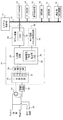
本発明の実施の形態を図を参照して説明する。図1は、本発明に係るモデム装置を用いた通信装置の概略構成を示したブロック図である。なお、このような通信装置としては、ファクシミリ装置、パーソナルコンピュータ、携帯端末等が例示でき、本実施の形態においてはファクシミリ装置を例に説明する。
【0018】
当該ファクシミリ装置は、システム制御部11を有し、このシステム制御部11にシステムバス12が接続され、当該システムバス12にプログラムROM13、データRAM14、操作表示部15、読取部16、記録部17、時計部18、モデム装置20が接続され、このモデム装置20に半導体プロセスによる半導体網制御部21が接続されて回線網と接続されている。
【0019】
半導体網制御部21は、回線電流を整流するダイオードブリッジ27を介して回線網に接続される1次側回路22、絶縁回路23、モデム装置20と接続される2次側回路24により形成された半導体DAAである。
【0020】
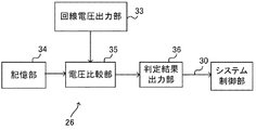
2次側回路24には、回線電圧をモニタしてそれを記憶して出力する回線電圧信号出力部25が設けられ、該回線電圧信号出力部25とシステム制御部11は外付電話オフフック判定回路26を介して接続されている。
【0021】
なお、ダイオードブリッジ27と1次側回路22との間には、回線網を外付電話に接続するか否かを制御する切断回路28が設けられ、また回線網と並列に外付電話が接続できるように外付電話端子29が設けられている。
【0022】
モデム装置20は、半導体プロセスにより作成されたDSP32を主要部品として構成され、該DSP32と2次側回路24とが接続されている。
【0023】
そして、1次側回路22は局給電により動作し、回線網からのアナログ信号をディジタル信号に変換するA/D−D/A変換器(CODEC)31を備えて、2次側回路24とのデータの受け渡しをディジタル信号で行い、着呼検出、回線網へ発呼処理、外付電話がオフフックされた際の切断回路28の駆動等の網制御や送受信データの送受信が行われるようになっている。
【0024】
システム制御部11は、プログラムROM13に格納された制御プログラムにしたがってデータRAM14を作業領域として使用しながら、各構成要素を制御している。
【0025】
システム制御部11は、省エネ時には電力供給が抑制される等の省エネ状態となり、このとき外付電話のオフフック等が検出されると、当該システム制御部11は通常状態に復帰して、検出した内容に応じて省エネ状態となっている機器を通常状態に復帰させるように制御する。
【0026】
ところで、省エネ状態とは、着呼等の受信待機中に必要となる機器以外の機器の動作が停止し又は抑制された状態で、システム制御部11、記録部17、読取部16、操作表示部15、DSP32、システムバス12等がかかる省エネ状態になり、省エネ時にはこれらの機器への電力供給が停止又は抑制される。
【0027】
電力供給の抑制方法として、例えば電流を制限したり動作周波数を下げたりすることが可能であり、動作周波数を変える場合には時計部18におけるクロック回路からの周波数を下げることにより行なわれる。
【0028】
データRAM14は、読取部16で読取った画情報をメモリ送信するために一時的にファイルとして蓄積する図示しない圧縮データメモリー用のSAFメモリ、受信した画情報を記録部17により記録するまでファイルとして一時的に蓄積してデータを記録する際に生データを展開する図示しないバッファ用のページメモリ等を備えて、図示しないバックアップ用回路によりバックアップされて装置電源遮断時にも記憶内容が保持されるようになっている。
【0029】
操作表示部15は、宛先電話番号を指定するためのテンキー、スタートキー、ワンタッチダイヤルキー及びその他各種キーを備え、また液晶表示装置等の表示器を備えて、ユーザに知らせるべき装置の動作状態や各種メッセージを表示する。
【0030】
読取部16は、3.85本/mm、7.7本/mm、15.4本/mm等の所定の読取線密度で原稿画像を読取って画情報を得るためのもので、読取った画情報は一旦ラインバッファに逐次蓄積されて必要とされる機器に転送されるようになっている。
【0031】
記録部17は、受信した画情報をその線密度に応じて記録出力したり、読取部16で読取った画情報をその線密度に応じて記録出力(コピー動作)するためのものであり、また管理リポートの出力にも用いられる。
【0032】
時計部18は、所定のクロック信号を発生するクロック回路を備え、現在時刻の計時を行う一方、システム制御部11から設定された時定数をカウントダウンしてタイムアウトするとシステム制御部11にタイムアウトしたことを通知する、タイマ動作を行うものである。
【0033】
DSP32は、送受信するデータを高速で変復調するもので、省エネ時には消費電力が抑制されるように電力供給を停止又は抑制されるようになっている。
【0034】
半導体網制御部21における、1次側回路22は、局給電により動作し2次側とデータの受け渡しを行うことによって回線網を制御し、2次側回路24は、送受信データをDSP32と1次側回路22と送受信できるようにするインターフェースの機能を持つ。
【0035】
また、当該2次側回路24における回線電圧信号出力部25は、回線電圧をモニタして、そのモニタ値を回線電圧レジスタ33に記憶し、この値をビット化して外付電話オフフック判定回路26に出力する。
【0036】
なお、絶縁回路23は、パルストランス、コンデンサ、フォトカプラ等から構成されて回線網と2次側回路24とを直流的に絶縁した状態で接続している。
【0037】
外付電話オフフック判定回路26は、DSP32と共にモデム装置20をなすもので、図2に示すように当該外付電話オフフック判定回路26は、記憶部34、電圧比較部35、判断結果出力部36により構成されている。
【0038】
記憶部34は、外付電話をオフフックした際の回線電圧を基準電圧として記憶する。日本国内の場合にはオフフックされると回線電圧が48Vから10V程度まで下がるので、この基準電圧としては例えば48Vとする。
【0039】
電圧比較部35は、回線電圧信号出力部33から回線電圧レジスタ33の値を回線電圧信号として取込むと共に記憶部34から基準電圧を取込み比較する。そして、これらが一致した場合には、外付電話がオフフックされたと判断する。
【0040】
判断結果出力部36は、電圧比較部35で外付電話がオフフックされたと判断した場合に、そのことを示すオフフック信号を専用ライン30を介してシステム制御部11に出力する。
【0041】
このような構成で、通常状態において外付電話がオフフックされると、その時の回線電圧のモニタ値が回線電圧信号出力部25の回線電圧レジスタ33に格納され、その値が回線電圧信号としてDSP32を介してシステム制御部11に出力される。
【0042】
そして、システム制御部11は、この回線電圧レジスタ33から外付電話がオフフックされているか否かを判断する。この判断は、プログラムROM13等からシステム制御部11に読込まれた基準電圧と回線電圧レジスタ33から取込んだ値を比較することにより行われる。
【0043】
そして、回線電圧レジスタ33から取込んだ値が基準電圧より低い場合には、外付電話がオフフックされたと判断し、48Vの場合にはオフフックされていないと判断する。
【0044】
無論、ファクシミリ装置本外が所定のファクシミリ通信を行う場合も、回線電圧は低下するが、この場合は必ずシステム制御部が関与した通信となる。これにより、ファクシミリ通信による回線電圧の低下か否かが判断でき、当該システム制御部が関与していないときに回線電圧が低下した場合には外付電話のオフフックと判断する。
【0045】
一方、ファクシミリ装置が省エネ状態に入っているときは、DSP32も省エネ状態となっているので、回線電圧レジスタ33の値はシステム制御部11に送られなくなり、外付電話のオフフックが検出できない。
【0046】
そこで、省エネ状態では外付電話オフフック判定回路26が起動して、回線電圧信号出力部25の回線電圧レジスタ33の値が外付電話オフフック判定回路26の電圧比較部35に送られて、ここで基準電圧と比較されて外付電話がオフフックされたか否かの判断が行われる。
【0047】
この判断により、外付電話がオフフックされたと判断すると、そのことを示すオフフック信号を専用ライン30を介してシステム制御部11に送る。
【0048】
これによりシステム制御部11は、省エネ状態からの復帰を制御して、切断回路28の制御信号をDSP32、2次側回路等を介して切断回路28に送り、回線網とファクシミリ装置本体との切離しを行う。
【0049】
そして、外付電話がオンフックされると回線電圧レジスタ33の値は、48V等の基準電圧となるので、この値がDSP32を介してシステム制御部11に送られ、当該システム制御部11は回線網とファクシミリ装置本体とが接続するように切断回路28を制御する。
【0050】
このとき、省エネ状態に移行する要件が満たされていれば、省エネ状態に移行するように制御する。
【0051】
以上により、省エネ時において2次側回路と接続されたDSP32を省エネ状態にしても、外付電話のオフフックが検出できるようになり、当該外付電話とファクシミリ装置との干渉を防止することが可能になる。
【0052】
なお、上記説明では、回線電圧レジスタ33の値を外付電話オフフック判定回路26に送る際に、回線電圧レジスタ33の値をビット化したディジタル信号で出力する場合について説明したが、本発明はこれに限定されるものではなく、回線電圧信号出力部25にA/D変換器を設けてアナログ信号に変換して送るようにしても良い。
【0053】
このように新たにA/D変換器を設けるとコストアップの要因となるが、アナログ信号で出力できるようにすることで接続端子数が削減できるため、これらのトレードオフの関係から結果的にコストダウンが可能になる利点がある。
【0054】
また、このようにアナログ信号により回線電圧信号を受取る構成では、外付電話オフフック判定回路26における基準電圧との比較がコンパレータ等により行えるようになるので、回路構成が簡単になる効果もある。
【0055】
ところで、これまでの説明では、外付電話オフフック判定回路26とDSP32とによりモデム装置20が構成される場合について説明したが、当該外付電話オフフック判定回路26をシステム制御部11内に設けても良く、また2次側回路24内に設けても良い。
【0056】
このように外付電話オフフック判定回路26をシステム制御部11内に設けたり、2次側回路26内に設けたりする場合には、システム制御部11及び2次側回路26が半導体プロセスにより形成されるために、当該外付電話オフフック判定回路26も半導体プロセスにより形成でき、独立して回路構成するよりもコストダウンが図れる利点がある。
【0057】
また、基準電圧は外付電話オフフック判定回路26の記憶部34に格納してオフフックの判断を行うようにしたが、当該記憶部34に相当する記憶手段をシステム制御部11に設けてもよい。この場合、通常状態では回線電圧レジスタ33の値がDSP32を介してシステム制御部11に送られ、省エネ状態では回線電圧レジスタ33の値が外付電話オフフック判定回路26を介してシステム制御部11に送られて、通常状態、省エネ状態共にシステム制御部11でオフフックの判断を行うことが可能になる。
【0058】
無論、記憶部34に相当する記憶手段を回線電圧信号出力部25に設けてもよい。この場合、
通常状態では回線電圧レジスタ33の値と基準電圧がDSP32を介してシステム制御部11に送られ、省エネ状態では回線電圧レジスタ33の値と基準電圧が外付電話オフフック判定回路26を介してシステム制御部11に送られて、通常状態、省エネ状態共にシステム制御部11でオフフックの判断を行うことが可能になる。
【0059】
次に、本発明の第2の実施の形態を図を参照して説明する。なお、上述した実施の形態と同一構成に関しては同一符号を用いて説明を適宜省略する。
【0060】
先に説明した実施の形態においては、基準電圧は予め設定された値であった。しかし、回線電圧は、交換機や回線路長等によって変動し、また日本では48Vであるが外国ではこの値と異なり、さらには内線交換機によっても異なる。
【0061】
従って、基準電圧を固定値にすると、このような使用環境により外付電話のオフフックの検出ができなくなる場合が発生する恐れがある。
【0062】
そこで、本実施の形態では、基準電圧を調整ができるようにして、使用環境により外付電話のオフフックの検出ができなくなる不都合を防止できるようにしたものである。
【0063】
この基準電圧を調整は、操作表示部15からユーザやサービスマンがキー入力等により入力して変更するようにする。
【0064】
これにより環境の違いによる回線電圧に違いがあっても、対応可能になり、利便性や信頼性が向上する。
【0065】
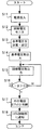
図3は、このような外付電話のオフフック検出手順を示すフローチャートである。先ず、基準電圧が変更されたか否かを判断し(ステップS1)、変更されている場合には変更後の基準電圧を用いる(ステップS2)。
【0066】
そして、この基準電圧をAとし、回線電圧信号出力部25からの回線電圧信号の値をBとして、これらの差分を求めて、その値が正か否かを判断する(ステップS3〜ステップS5)。
【0067】
この差分値が正の場合は、オフフックにより回線電圧が下がった結果、回線電圧が基準電圧より小さくなったと考えて外付電話がオフフックとなったと判断し(ステップS6)、その旨をシステム制御部11側に通知する(ステップS7)。
【0068】
以上により省エネ時にモデム装置20への電源供給を停止又は抑制しても外付電話のオフフックが判断できるようなり、省エネ効果が向上すると共に利便性が向上する。
【0069】
また、基準電圧を変更できるようにすることにより、使用環境等に適した基準電圧値が設定できるようになるので利便性が向上する。
【0070】
次に、本発明の第3の実施の形態を図を参照して説明する。なお、上述した実施の形態と同一構成に関しては同一符号を用いて説明を適宜省略する。
【0071】
第2の実施の形態では、基準電圧の設定はユーザ等が行った。これに対して、本実施の形態では自動設定できるようにしたものである。
【0072】
即ち、ユーザ等が基準電圧の設定を行う場合には、どのような値に基準電圧を設定すべきかを知る必要があり、かかる値は回線網の状況に依るため一般ユーザにとって設定が困難となる。従って、このような設定はサービスマン等の専門の知識を有する人に頼らざるを得なくなる場合が多い。
【0073】
そこで、オフフックすると回線電圧が降下することから、システム電源が投入された後の回線電圧を検出し、その値に対して予め設定された割合だけ小さい値(例えば1/2や1/3の値)を演算して基準電圧として設定する。
【0074】
但し、電圧が極端に低い場合は、電源時点で既に外付電話がオフフックされ又は回線抜けしている場合が考えられるため変更しない。
【0075】
図4は、このような基準電圧の自動変更を行う際の処理手順を示すフローチャートで、システム電源が投入されると(ステップS11)、回線電圧のモニタが行われ(ステップS12)、その検出値に基づき基準電圧を演算して設定する(ステップS13)。
【0076】
このようにして基準電圧の変更が行われた状態で、この基準電圧をAとし、回線電圧信号出力部25からの回線電圧をBとして、これらの差分を求めて、その値が正か否かを判断する(ステップS14〜ステップS16)。
【0077】
この差分値が正の場合は、オフフックにより回線電圧が下がった結果、回線電圧が基準電圧より小さくなったと考えて、外付電話がオフフックとなったと判断して(ステップS17)、その旨をシステム制御部11側に通知する(ステップS18)。
【0078】
なお、電源投入された後の回線電圧を検出し、その後に外付電話をオフフックして、その時の回線電圧を検出して、オフフック前後の回線電圧値からその中間の値を基準電圧とするようにしてもよい。
【0079】
このような基準電圧の自動設定時には、上述したようにシステム電源が投入されたときでありシステム制御部11が判断するので、当該システム制御部11は省エネ状態ではなく通常動作状態である。従って、回線電圧の検出信号はモデム装置20を介して受信する。
【0080】
【発明の効果】
上記課題を解決するため、モデム装置にかかる発明によれば、モデム装置のDSPへの電力供給が停止又は抑制されている際に、半導体DAAの2次側回路からの信号に基づき外付電話のオフフックを検出して、その検出結果を出力する外付電話オフフック判定回路を設けたので、省エネ時においてはDSPを介さずにオフフックが検出できるようになり省エネ効果を高めることが可能になる。
【0081】
また、通信装置にかかる発明は、省エネ状態ではモデム装置のDSPへの電力供給が停止又は抑制され、この省エネ状態の間に2次側回路からの信号に基づき外付電話のオフフックを検出すると、専用ラインを介してシステム制御部に出力する外付電話オフフック判定回路を設けたので、省エネ時においてはDSPを介さずにオフフックが検出できるようになり省エネ効果を高めることが可能になる。
【図面の簡単な説明】
【図1】本発明の第1〜第3実施の形態の説明に適用される通信装置のブロック図である。
【図2】外付電話オフフック判定回路のブロックである。
【図3】第2の実施の形態の説明に適用される外付電話オフフック判定手順を示すフローチャートである。
【図4】第3の実施の形態の説明に適用される外付電話オフフック判定手順を示すフローチャートである。
【符号の説明】
11 システム制御部
12 システムバス
15 操作表示部
18 時計部
20 モデム装置
21 半導体網制御部
23 絶縁回路
22 1次側回路
24 2次側回路
25 回線電圧信号出力部
26 外付電話オフフック判定回路
28 切断回路
29 外付電話端子
30 専用ライン
32 DSP
33 回線電圧信号出力部
33 回線電圧レジスタ
34 記憶部
35 電圧比較部
36 判断結果出力部[0001]
BACKGROUND OF THE INVENTION
The present invention relates to the above-described 2 in a semiconductor DAA (Data Access Arrangement) composed of a primary side circuit connected to a circuit network and a secondary side circuit connected to the primary side circuit via an insulating circuit. When a DSP (Digital Signal Processor) that modulates and demodulates data is connected to the secondary circuit, a modem device that can detect an off-hook of an external telephone without going through the DSP even when the DSP is in an energy saving state The present invention relates to a communication device using the.
[0002]
[Prior art]
In recent years, with the spread of the Internet, digital mobile phones, and the like, communication devices such as mobile terminals and small terminals have been downsized.
[0003]
However, a communication device with a built-in modem connected to a public network requires a relatively large transformer for the purpose of DC insulation for connection to the network, and this transformer hinders downsizing of the communication device. It was a factor.
[0004]
However, with recent advances in semiconductor process technology and isolation technology, semiconductor DAAs that perform network control and the like have been developed, and the function of the lance can be replaced with an extremely small pulse transformer, capacitor, photocoupler, or the like. It has become possible (see Patent Document 1).
[0005]
Such functional elements formed of semiconductors are expected to reduce the size and cost of communication devices, and are being sought for use in communication devices that are not portable terminals such as facsimile devices.
[0006]
Such a communication apparatus requires a network control function for controlling the network, a modulation / demodulation function for performing modulation / demodulation of signals transmitted / received via the network.
[0007]
As described above, the network control function is made semiconductor by the semiconductor DAA, and the modulation / demodulation function is called a so-called modem. Today, a DSP formed by a semiconductor process is used as a main part to perform high-speed processing. Yes.
[0008]
Accordingly, both the network control function and the modulation / demodulation function, which are the minimum functions necessary for communication, are supplied as a semiconductor.
[0009]
[Patent Document 1]
Japanese Patent Laid-Open No. 06-098038
[Problems to be solved by the invention]
However, communication devices are strongly required to reduce power consumption from the viewpoint of environmental considerations, etc., and in order to respond to this, energy saving functions are becoming almost standard equipment. Since it is directly connected to the DSP of the modem device responsible for the modulation / demodulation function, there is a problem that it is impossible to detect the off-hook of the external telephone unless the DSP is supplied with the same power as in the normal state even in the energy saving state.
[0011]
That is, the modem apparatus performs modulation / demodulation of data as described above, but it is necessary to perform modulation / demodulation processing at high speed from the viewpoint of increasing the amount of data to be handled. For this reason, a DSP in which a function responsible for modulation / demodulation is made into a semiconductor is used, and its operating frequency is high. As the operating frequency increases, the power consumption increases accordingly.
[0012]
On the other hand, in the energy saving state, the power supply to the minimum equipment necessary for reception is stopped or suppressed to reduce power consumption. However, the DSP is connected to the semiconductor DAA and detected by the semiconductor DAA. Since the off-hook of the external telephone is informed to the communication apparatus main body side through the DSP, the power supply to the DSP must be supplied in the same manner as in the normal state even in the energy saving state.
[0013]
Therefore, since the semiconductor DAA is used, the power consumption is increased in the state where the same power is supplied to the DSP even during energy saving as compared with the case where the DSP is brought into the energy saving state without using the semiconductor DAA.
[0014]
SUMMARY OF THE INVENTION An object of the present invention is to provide a modem device and a communication device using the same so that off-hook can be detected without going through a DSP during energy saving so that the energy saving effect can be enhanced.
[0015]
[Means for Solving the Problems]
In order to solve the above problems, an invention relating to a modem device includes a primary side circuit connected to a line network and a secondary side circuit connected to the primary side circuit via an insulation circuit. connected to the secondary circuit of the semiconductor DAA transmitting and receiving data includes a DSP for performing modulation and demodulation of data transmitted and received to control the in modem device used by being connected by the communication device main body and the system bus, wherein The storage unit for storing the line voltage when the external telephone is off-hooked as a reference voltage and the line voltage signal and the reference voltage are compared. If they match, it is determined that the external telephone is off-hook. A voltage comparison unit, and a determination result output unit that outputs an off-hook signal indicating that when the external phone is off-hooked by the voltage comparison unit, Is connected to the serial secondary circuit, the power supply to the DSP is when being stopped or suppressed, characterized in that a external telephone off-hook determination circuit for detecting an off-hook of the External telephone.
[0016]
According to another aspect of the present invention, there is provided a communication device comprising a primary circuit connected to a network and a secondary circuit connected to the primary circuit via an insulation circuit, and controls the network and data. A modem device including a semiconductor DAA that transmits / receives data, a DSP that is connected to the secondary circuit and performs modulation / demodulation of data to be transmitted / received, and is connected to the DSP by a system bus to control the semiconductor DAA and the modem device. And a system control unit that communicates with each other and has an energy-saving function that shifts from the normal state to the energy-saving state when the predetermined energy-saving transition requirement is satisfied, and shifts from the energy-saving state to the normal state when the predetermined return requirement is satisfied in the communication apparatus, the modem device, a storage unit for storing the line voltage at the time of off-hook the External telephone as the reference voltage, the line voltage signal and said reference voltage and In comparison, if they match, the voltage comparison unit determines that the external telephone is off-hook, and if the voltage comparison unit determines that the external telephone is off-hook, the off-hook indicating that fact. A determination result output unit for outputting a signal, connected to the secondary side circuit, and when the off-hook of the external telephone is detected when power supply to the DSP is stopped or suppressed, a dedicated line And an external telephone off-hook determination circuit for outputting via the network.
[0017]
DETAILED DESCRIPTION OF THE INVENTION
Embodiments of the present invention will be described with reference to the drawings. FIG. 1 is a block diagram showing a schematic configuration of a communication device using a modem device according to the present invention. Note that examples of such a communication apparatus include a facsimile machine, a personal computer, a portable terminal, and the like. In this embodiment, a facsimile machine will be described as an example.
[0018]
The facsimile apparatus includes a
[0019]
The semiconductor
[0020]
The
[0021]
A disconnect circuit 28 for controlling whether or not the line network is connected to the external telephone is provided between the
[0022]
The
[0023]
The primary side circuit 22 operates by local power supply and includes an A / D-D / A converter (CODEC) 31 that converts an analog signal from the network into a digital signal. Data is exchanged by digital signals, network control such as detection of incoming calls, call processing to the network, driving of the disconnection circuit 28 when the external telephone is off-hook, and transmission / reception of transmission / reception data are performed. Yes.
[0024]
The
[0025]
The
[0026]
By the way, the energy saving state is a state in which the operation of devices other than the devices required during reception waiting for an incoming call or the like is stopped or suppressed, and the
[0027]
As a method for suppressing power supply, for example, the current can be limited or the operating frequency can be lowered. When the operating frequency is changed, the frequency from the clock circuit in the
[0028]
The
[0029]
The
[0030]
The
[0031]
The recording unit 17 records and outputs the received image information in accordance with the linear density, and records and outputs the image information read by the
[0032]
The
[0033]
The
[0034]
The primary side circuit 22 in the semiconductor
[0035]
Further, the line voltage
[0036]
The insulating circuit 23 includes a pulse transformer, a capacitor, a photocoupler, and the like, and connects the line network and the
[0037]
The external telephone off-
[0038]
The
[0039]
The
[0040]
When the
[0041]
With this configuration, when the external telephone is off-hooked in a normal state, the monitor value of the line voltage at that time is stored in the
[0042]
Then, the
[0043]
When the value fetched from the
[0044]
Of course, the line voltage also decreases when the facsimile apparatus outside performs a predetermined facsimile communication. In this case, however, the communication always involves the system control unit. Accordingly, it can be determined whether or not the line voltage is reduced due to facsimile communication. If the line voltage is reduced when the system control unit is not involved, it is determined that the external telephone is off-hook.
[0045]
On the other hand, when the facsimile apparatus is in the energy saving state, the
[0046]
Therefore, in the energy saving state, the external telephone off-
[0047]
If it is determined by this determination that the external telephone is off-hook, an off-hook signal indicating that is sent to the
[0048]
As a result, the
[0049]
When the external telephone is on-hooked, the value of the
[0050]
At this time, if the requirement to shift to the energy saving state is satisfied, control is performed to shift to the energy saving state.
[0051]
As described above, even when the
[0052]
In the above description, when the value of the
[0053]
Although providing a new A / D converter in this way increases the cost, the number of connection terminals can be reduced by enabling output as an analog signal, resulting in a cost resulting from these trade-offs. There is an advantage that down is possible.
[0054]
Further, in the configuration in which the line voltage signal is received by the analog signal as described above, the comparison with the reference voltage in the external telephone off-
[0055]
In the above description, the case where the
[0056]
As described above, when the external telephone off-
[0057]
Further, although the reference voltage is stored in the
[0058]
Of course, a storage means corresponding to the
In the normal state, the value of the
[0059]
Next, a second embodiment of the present invention will be described with reference to the drawings. Note that the same components as those in the above-described embodiment are denoted by the same reference numerals and description thereof is omitted as appropriate.
[0060]
In the embodiment described above, the reference voltage is a preset value. However, the line voltage varies depending on the exchange, the line length, etc., and is 48V in Japan, but is different from this value in foreign countries, and also differs depending on the extension exchange.
[0061]
Accordingly, when the reference voltage is set to a fixed value, there is a possibility that off-hook detection of the external telephone cannot be detected due to such a use environment.
[0062]
Therefore, in this embodiment, the reference voltage can be adjusted to prevent the inconvenience that the off-hook of the external telephone cannot be detected depending on the use environment.
[0063]
The reference voltage is adjusted by a user or a serviceman who input from the
[0064]
As a result, even if there is a difference in line voltage due to a difference in environment, it becomes possible to cope with it, and convenience and reliability are improved.
[0065]
FIG. 3 is a flowchart showing an off-hook detection procedure for such an external telephone. First, it is determined whether or not the reference voltage has been changed (step S1). If the reference voltage has been changed, the changed reference voltage is used (step S2).
[0066]
Then, assuming that the reference voltage is A and the value of the line voltage signal from the line voltage
[0067]
If this difference value is positive, it is determined that the line voltage has become lower than the reference voltage as a result of the line voltage being lowered due to off-hook, and it is determined that the external telephone is off-hook (step S6). 11 side (step S7).
[0068]
As described above, even when the power supply to the
[0069]
Further, by making it possible to change the reference voltage, it becomes possible to set a reference voltage value suitable for the usage environment and the convenience is improved.
[0070]
Next, a third embodiment of the present invention will be described with reference to the drawings. Note that the same components as those in the above-described embodiment are denoted by the same reference numerals and description thereof is omitted as appropriate.
[0071]
In the second embodiment, the reference voltage is set by the user or the like. On the other hand, in this embodiment, automatic setting can be performed.
[0072]
That is, when a user or the like sets a reference voltage, it is necessary to know what value the reference voltage should be set to, and such a value depends on the state of the line network and is difficult for a general user to set. . Therefore, in many cases, such setting must be relied upon by a person having specialized knowledge such as a service person.
[0073]
Therefore, since the line voltage drops when off-hook, the line voltage after the system power is turned on is detected, and a value smaller by a preset ratio (for example, a value of 1/2 or 1/3). ) And set as the reference voltage.
[0074]
However, if the voltage is extremely low, there is a possibility that the external telephone is already off-hooked or disconnected from the line at the time of power supply.
[0075]
FIG. 4 is a flowchart showing a processing procedure for automatically changing such a reference voltage. When the system power is turned on (step S11), the line voltage is monitored (step S12), and the detected value is detected. The reference voltage is calculated and set based on (step S13).
[0076]
In the state where the reference voltage is changed in this way, the reference voltage is set to A, the line voltage from the line voltage
[0077]
If this difference value is positive, it is determined that the line voltage has become lower than the reference voltage as a result of the line voltage being lowered due to off-hook, and it is determined that the external telephone is off-hook (step S17). The
[0078]
Note that the line voltage after the power is turned on is detected, then the external telephone is off-hooked, the line voltage at that time is detected, and an intermediate value from the line voltage values before and after the off-hook is set as the reference voltage. It may be.
[0079]
When the reference voltage is automatically set, the
[0080]
【The invention's effect】
In order to solve the above-described problem, according to the invention relating to the modem device, when the power supply to the DSP of the modem device is stopped or suppressed, the external telephone is connected based on the signal from the secondary circuit of the semiconductor DAA. Since the external telephone off-hook determination circuit for detecting the off-hook and outputting the detection result is provided, the off-hook can be detected without going through the DSP at the time of energy saving, and the energy saving effect can be enhanced.
[0081]
Further, in the invention related to the communication device, power supply to the DSP of the modem device is stopped or suppressed in the energy saving state, and when the off-hook of the external telephone is detected based on a signal from the secondary side circuit during the energy saving state, Since the external telephone off-hook determination circuit for outputting to the system control unit via the dedicated line is provided, the off-hook can be detected without using the DSP during energy saving, and the energy saving effect can be enhanced.
[Brief description of the drawings]
FIG. 1 is a block diagram of a communication device applied to the description of first to third embodiments of the present invention.
FIG. 2 is a block diagram of an external telephone off-hook determination circuit.
FIG. 3 is a flowchart showing an external telephone off-hook determination procedure applied to the description of the second embodiment.
FIG. 4 is a flowchart showing an external telephone off-hook determination procedure applied to the description of the third embodiment.
[Explanation of symbols]
11
33 Line voltage
Claims (20)
前記外付電話をオフフックした際の回線電圧を基準電圧として記憶する記憶部と、
前記回線電圧信号と前記基準電圧とを比較して、これらが一致した場合には前記外付電話がオフフックされたと判断する電圧比較部と、
該電圧比較部で前記外付電話がオフフックされたと判断した場合には、そのことを示すオフフック信号を出力する判断結果出力部とを備え、
前記2次側回路と接続されて、前記DSPへの電力供給が停止又は抑制されている際に、前記外付電話のオフフックを検出する外付電話オフフック判定回路を設けたことを特徴とするモデム装置。The semiconductor DAA 2 includes a primary circuit connected to a network and a secondary circuit connected to the primary circuit via an insulating circuit, and controls the network and transmits / receives data. In a modem device which is connected to a communication device main body and used by a system bus, and has a DSP which modulates and demodulates data to be transmitted / received by being connected to a secondary circuit,
A storage unit for storing a line voltage when the external telephone is off-hook as a reference voltage;
A voltage comparison unit that compares the line voltage signal and the reference voltage and determines that the external telephone is off-hook when they match;
When the voltage comparison unit determines that the external telephone is off-hook, the voltage comparison unit includes a determination result output unit that outputs an off-hook signal indicating that,
A modem connected to the secondary circuit and provided with an external telephone off-hook determination circuit for detecting an off-hook of the external telephone when power supply to the DSP is stopped or suppressed apparatus.
前記外付電話オフフック判定回路が、前記回線電圧信号に基づき外付電話がオフフックされたか否かを判定することを特徴とする請求項1記載のモデム装置。The secondary circuit includes a line voltage register that monitors and stores the line voltage, and has a line voltage signal output unit that outputs a signal corresponding to the line voltage register value as a line voltage signal;
2. The modem apparatus according to claim 1, wherein the external telephone off-hook determination circuit determines whether or not the external telephone is off-hook based on the line voltage signal.
前記モデム装置が、
前記外付電話をオフフックした際の回線電圧を基準電圧として記憶する記憶部と、
前記回線電圧信号と前記基準電圧とを比較して、これらが一致した場合には前記外付電話がオフフックされたと判断する電圧比較部と、
該電圧比較部で前記外付電話がオフフックされたと判断した場合には、そのことを示すオフフック信号を出力する判断結果出力部とを備え、
前記2次側回路と接続されて、前記DSPへの電力供給が停止又は抑制されている際に、前記外付電話のオフフックを検出すると、専用ラインを介して出力する外付電話オフフック判定回路を備えたことを特徴とする通信装置。A semiconductor DAA which comprises a primary side circuit connected to a line network and a secondary side circuit connected to the primary side circuit via an insulation circuit, which controls the line network and transmits / receives data; A modem device having a DSP connected to the secondary side circuit for performing modulation / demodulation of data to be transmitted and received, and a system control unit connected to the DSP by a system bus to control and communicate with the semiconductor DAA and the modem device In a communication device with an energy saving function that shifts from a normal state to an energy saving state when a predetermined energy saving transition requirement is satisfied, and shifts from an energy saving state to a normal state when a predetermined return requirement is satisfied,
The modem device is
A storage unit for storing a line voltage when the external telephone is off-hook as a reference voltage;
A voltage comparison unit that compares the line voltage signal with the reference voltage and determines that the external telephone is off-hook when they match;
When the voltage comparison unit determines that the external telephone is off-hook, the voltage comparison unit includes a determination result output unit that outputs an off-hook signal indicating that,
An external telephone off-hook determination circuit that outputs via a dedicated line when an off-hook of the external telephone is detected when the power supply to the DSP is stopped or suppressed while being connected to the secondary circuit. A communication apparatus comprising:
前記外付電話オフフック判定回路が、前記回線電圧信号に基づき外付電話がオフフックされたか否かを判定することを特徴とする請求項10記載の通信装置。The secondary circuit includes a line voltage register that monitors and stores the line voltage, and has a line voltage signal output unit that outputs a signal corresponding to the line voltage register value as a line voltage signal;
11. The communication apparatus according to claim 10, wherein the external telephone off-hook determination circuit determines whether or not the external telephone is off-hook based on the line voltage signal.
Priority Applications (1)
| Application Number | Priority Date | Filing Date | Title |
|---|---|---|---|
| JP2002275654A JP3920182B2 (en) | 2002-09-20 | 2002-09-20 | MODEM DEVICE AND COMMUNICATION DEVICE |
Applications Claiming Priority (1)
| Application Number | Priority Date | Filing Date | Title |
|---|---|---|---|
| JP2002275654A JP3920182B2 (en) | 2002-09-20 | 2002-09-20 | MODEM DEVICE AND COMMUNICATION DEVICE |
Publications (2)
| Publication Number | Publication Date |
|---|---|
| JP2004112679A JP2004112679A (en) | 2004-04-08 |
| JP3920182B2 true JP3920182B2 (en) | 2007-05-30 |
Family
ID=32271788
Family Applications (1)
| Application Number | Title | Priority Date | Filing Date |
|---|---|---|---|
| JP2002275654A Expired - Fee Related JP3920182B2 (en) | 2002-09-20 | 2002-09-20 | MODEM DEVICE AND COMMUNICATION DEVICE |
Country Status (1)
| Country | Link |
|---|---|
| JP (1) | JP3920182B2 (en) |
-
2002
- 2002-09-20 JP JP2002275654A patent/JP3920182B2/en not_active Expired - Fee Related
Also Published As
| Publication number | Publication date |
|---|---|
| JP2004112679A (en) | 2004-04-08 |
Similar Documents
| Publication | Publication Date | Title |
|---|---|---|
| JPH1065866A (en) | Facsimile equipment | |
| JP2013005037A (en) | Facsimile apparatus | |
| US7139104B2 (en) | Downsized facsimile machine using semiconductor DAA | |
| JP3920182B2 (en) | MODEM DEVICE AND COMMUNICATION DEVICE | |
| JP3961934B2 (en) | Facsimile device | |
| JP4060677B2 (en) | Modem equipment | |
| JP7447504B2 (en) | Communication device, connection state detection method, and program | |
| JP5790182B2 (en) | Facsimile machine | |
| JP4499644B2 (en) | Terminal network controller | |
| JP3991951B2 (en) | Facsimile device | |
| JP2001053895A (en) | Facsimile terminal | |
| JP5824934B2 (en) | Communication terminal device | |
| JP2004112680A (en) | Communication system | |
| JP3968708B2 (en) | Communication device | |
| JP2016036116A (en) | Communication apparatus, control method of the same, and program | |
| JPH1146275A (en) | Facsimile equipment | |
| JP2003189022A (en) | Facsimile machine | |
| US6456401B1 (en) | Communication apparatus capable of conducting remote diagnosis using communication circuit | |
| JP2009111648A (en) | Facsimile machine and program | |
| JPH066503A (en) | Facsimile equipment | |
| JPH07123237A (en) | Facsimile equipment | |
| JP2004104557A (en) | Facsimile equipment | |
| JP2000349930A (en) | Communication terminal equipment | |
| JP2004343455A (en) | Communication terminal | |
| JPH10215364A (en) | Facsimile equipment |
Legal Events
| Date | Code | Title | Description |
|---|---|---|---|
| A621 | Written request for application examination |
Free format text: JAPANESE INTERMEDIATE CODE: A621 Effective date: 20050218 |
|
| A977 | Report on retrieval |
Free format text: JAPANESE INTERMEDIATE CODE: A971007 Effective date: 20061109 |
|
| A131 | Notification of reasons for refusal |
Free format text: JAPANESE INTERMEDIATE CODE: A131 Effective date: 20061121 |
|
| A521 | Written amendment |
Free format text: JAPANESE INTERMEDIATE CODE: A523 Effective date: 20070119 |
|
| TRDD | Decision of grant or rejection written | ||
| A01 | Written decision to grant a patent or to grant a registration (utility model) |
Free format text: JAPANESE INTERMEDIATE CODE: A01 Effective date: 20070213 |
|
| A61 | First payment of annual fees (during grant procedure) |
Free format text: JAPANESE INTERMEDIATE CODE: A61 Effective date: 20070214 |
|
| R150 | Certificate of patent or registration of utility model |
Free format text: JAPANESE INTERMEDIATE CODE: R150 |
|
| FPAY | Renewal fee payment (event date is renewal date of database) |
Free format text: PAYMENT UNTIL: 20110223 Year of fee payment: 4 |
|
| FPAY | Renewal fee payment (event date is renewal date of database) |
Free format text: PAYMENT UNTIL: 20120223 Year of fee payment: 5 |
|
| FPAY | Renewal fee payment (event date is renewal date of database) |
Free format text: PAYMENT UNTIL: 20130223 Year of fee payment: 6 |
|
| FPAY | Renewal fee payment (event date is renewal date of database) |
Free format text: PAYMENT UNTIL: 20130223 Year of fee payment: 6 |
|
| FPAY | Renewal fee payment (event date is renewal date of database) |
Free format text: PAYMENT UNTIL: 20140223 Year of fee payment: 7 |
|
| LAPS | Cancellation because of no payment of annual fees |