JP3917543B2 - Induction heating fixing device - Google Patents
Induction heating fixing device Download PDFInfo
- Publication number
- JP3917543B2 JP3917543B2 JP2003085900A JP2003085900A JP3917543B2 JP 3917543 B2 JP3917543 B2 JP 3917543B2 JP 2003085900 A JP2003085900 A JP 2003085900A JP 2003085900 A JP2003085900 A JP 2003085900A JP 3917543 B2 JP3917543 B2 JP 3917543B2
- Authority
- JP
- Japan
- Prior art keywords
- bobbin
- wire
- coil
- main body
- electric wire
- Prior art date
- Legal status (The legal status is an assumption and is not a legal conclusion. Google has not performed a legal analysis and makes no representation as to the accuracy of the status listed.)
- Expired - Fee Related
Links
Images

Landscapes
- Fixing For Electrophotography (AREA)
- General Induction Heating (AREA)
Description
【0001】
【発明の属する技術分野】
本発明は複写機やプリンタなどの画像形成装置に搭載され、用紙上の現像剤像を定着させる定着装置に関する。
【0002】
【従来の技術】
デジタル技術を利用した画像形成装置たとえば電子複写機では、原稿が載置された原稿台が露光され、その原稿台からの反射光が光電変換素子たとえばCCD(charge coupled device)に導かれる。
【0003】
CCDは、原稿の画像に対応する画像信号を出力する。この画像信号に応じたレーザ光が感光体ドラムに照射されて、感光体ドラムの周面に静電潜像が形成される。この静電潜像は、現像剤(トナー)の付着により顕像化される。感光体ドラムには、その感光体ドラムの回転にタイミングを合わせて用紙が送られており、その用紙に感光体ドラム上の顕像(現像剤像)が転写される。現像剤像が転写された用紙は、定着装置に送られる。
【0004】
定着装置は、加熱ローラと、この加熱ローラに加圧状態で接しながらその加熱ローラと共に回転する加圧ローラとを備え、この両ローラ間に用紙を挟み込んでその用紙を搬送しながら、加熱ローラの熱によって用紙上の現像剤像を定着させる。
【0005】
加熱ローラの熱源として、誘導加熱がある。これは、加熱ローラ内にコイルを収め、そのコイルにコンデンサを接続して共振回路を形成し、その共振回路を1つの共振回路に対して1つの周波数で励起することによりコイルに高周波電流を流してコイルから高周波磁界を発生させ、その高周波磁界によって加熱ローラに渦電流を生じさせ、その渦電流によるジュール熱で加熱ローラを自己発熱させる。
【0006】
この誘導加熱を利用した定着装置は、金属導電体からなる定着ローラを電磁波による渦電流によって加熱するもので、定着ローラ内に非磁性体のボビンに螺旋状に巻装された誘導コイルが設けられ、この誘導コイルに高周波電流を流すことによって、これによって生じた高周波磁界で定着ローラに誘導渦電流を発生させ、定着ローラの表皮抵抗によって定着ローラそのものをジュール熱によって発熱させている。このボビンは製造を容易に行ない修理も簡単に行う目的で、中央の主ボビン部材とその両側に連結される従ボビン部材の3個に分割し、分割されたボビン部材の夫々に導線を巻回して誘導コイルを構成している(例えば、特許文献1参照)。
【0007】
【特許文献1】
特開2001−312165号公報(第2−3頁、図1)
【0008】
【発明が解決しようとする課題】
近年、省エネ対応技術としてW/Uの短縮化が技術課題となっているが、対策として加熱ローラの薄肉化が上げられる。しかしながら、定着装置においては多種の紙サイズが用いられるため、幅の狭い用紙が連続で通紙されることにより、加熱ローラ上の前記用紙の外側が用紙に熱を奪われないために用紙幅内の温度に比べて高くなることで、高温になったり、幅の狭い用紙の後に幅の広い用紙を通紙されると高温オフセットによる定着不良が発生してしまうという現象は加熱ローラの肉厚が薄いほど(熱容量が小さいほど)顕著になる。
【0009】
また、定着装置を構成するコイルの製造にあっては、更なる効率化及び製造の容易性等が求められてきている。
【0010】
この発明は上記の事情を考慮したもので、その目的とするところは、上記のような問題点を解消することができる実用性および信頼性にすぐれた誘導加熱定着装置を提供することにある。
【0011】
【課題を解決するための手段】
本発明は上記課題を解決するための手段として、渦電流の発生により発熱する被加熱部材と、本体に電線を複数回巻きつけてなり、両端部に前記電線の入力側と出力側を夫々導く溝部を有するボビン、及び前記ボビンを複数個支持するホルダ、並びに前記ボビンの内側に配置され、前記本体から引き出されて前記溝部を経た前記電線を通過させて、前記ホルダの端部方向に導く電線ガイドを有し、前記本体に表記され、前記溝部にある前記電線を識別する符号、及び前記電線ガイドに表記され、前記電線ガイドにある前記電線を識別する符号を参照して、前記ボビンの方向を定めて前記ホルダに複数個挿通することにより組み立てられるコイルユニットを、前記被加熱部材に複数個隣接配置してなり、前記被加熱部材に前記渦電流を発生させるコイルユニット群と、前記被加熱部材に接触して記録媒体を所定の圧力を持って、前記被加熱部材と共に挟持搬送する加圧部材とを具備するものである。
【0012】
【発明の実施の形態】
以下、この発明の実施の形態について図面を参照して説明する。
【0013】
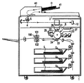
まず、画像形成装置たとえば複合型電子複写機の内部の構成を図1に示している。本体1の上面部に原稿載置用の透明の原稿台(ガラス板)2が設けられており、キャリッジ4に設けられた露光ランプ5が点灯することにより、原稿台2に載置されている原稿Dが露光される。
【0014】
この露光による反射光が光電変換素子たとえばCCD(Charge Coupled Device)10に投影されることで画像信号が出力される。CCD10から出力される画像信号は、デジタル信号に変換され、そのデジタル信号が適宜に処理された後、レーザユニット27に供給される。レーザユニット27は、入力信号に応じてレーザビームBを発する。
【0015】
本体1の上面部において、自動原稿送りユニット40が被さらない位置に、図示していないが、動作条件設定用のコントロールパネルが設けられている。コントロールパネルは、タッチパネル式の液晶表示部、数値入力用のテンキー、コピーキーなどを備えている。
【0016】
一方、本体1内の略中央部に、感光体ドラム20が回転自在に設けられている。この感光体ドラム20の周囲に、帯電器21、現像ユニット22、転写器23、剥離器24、クリーナ25、除電器26が順次に配設されており、既知のプロセス方法にて感光体ドラム20上にトナー画像が形成され、用紙上にトナー画像が転写、後述の定着装置100により、用紙上のトナーが加熱・加圧定着される。
【0017】
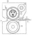
定着装置100の具体的な構成を図2に示している。
【0018】
コピー用紙Sの搬送路を上下に挟む位置に、加熱ローラ101および加圧ローラ102が設けられている。加圧ローラ102は、図示していない加圧機構により、加熱ローラ101の周面に加圧状態で接している。これらローラ101,102の接触部は一定のニップ幅を持つ。
【0019】
加熱ローラ101は、導電性材料たとえば鉄を筒状に成形し、その鉄の外周面にテフロン等を被覆したもので、図示右方向に回転駆動される。加圧ローラ102は、加熱ローラ101の回転を受けて図示左方向に回転する。この加熱ローラ101と加圧ローラ102との接触部をコピー用紙Sが通過し、かつコピー用紙Sが加熱ローラ101から熱を受けることにより、コピー用紙S上の現像剤像Tがコピー用紙Sに定着される。
【0020】
加熱ローラ101の周囲に、コピー用紙Sを加熱ローラ101から剥離するための剥離爪103、加熱ローラ101上に残るトナーおよび紙屑等を除去するためのクリーニング部材104、加熱ローラ101の表面に離型剤を塗布するための塗布ローラ105が配設されている。
【0021】
加熱ローラ101の内部に、誘導加熱用のコイルユニット群であるコイル111が収容されている。コイル111は、ボビン112に巻回および保持され、誘導加熱用の高周波磁界を発する。この高周波磁界が発せられることにより、加熱ローラ101に渦電流が生じ、その渦電流によるジュール熱で加熱ローラ101が自己発熱する。
【0022】
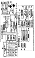
本体1の制御回路を図3に示している。
【0023】
メインCPU50に、スキャンCPU70、コントロールパネルCPU80、およびプリントCPU90が接続されている。メインCPU50は、スキャンCPU70、コントロールパネルCPU80、およびプリントCPU90を統括的に制御するもので、コピーキーの操作に応じたコピーモードの制御手段、後述のネットインタフェース59への画像入力に応じたプリンタモードの制御手段、および後述のFAX送受信ユニット60での画像受信に応じたFAX(ファクシミリ)モードの制御手段を備えている。
【0024】
また、メインCPU50に、制御プログラム記憶用のROM51、データ記憶用のRAM52、画素カウンタ53、画像処理部55、ページメモリコントローラ56、ハードディスクユニット58、ネットインタフェース59、およびFAX送受信ユニット60が接続されている。ページメモリコントローラ56は、ページメモリ57に対する画像データの書込みおよび読出しを制御する。そして、画像データバス61により、画像処理部55、ページメモリコントローラ56、ページメモリ57、ハードディスクユニット58、ネットインタフェース59、およびFAX送受信ユニット60が相互に接続されている。
【0025】
上記ネットインタフェース59は、外部機器から伝送されてくる画像(画像データ)が入力されるプリンタモード用の入力部として機能する。このネットインタフェース59にLANあるいはインターネットなどの通信ネットワーク201が接続され、その通信ネットワーク201に外部機器たとえば複数台のパーソナルコンピュータ202が接続されている。これらパーソナルコンピュータ202は、コントローラ203、ディスプレイ204、操作ユニット205を備えている。
【0026】
上記FAX送受信ユニット60は、電話回線210に接続されており、その電話回線210を通してファクシミリ送信されてくる画像(画像データ)を受信するファクシミリモード用の受信部として機能する。
【0027】
スキャンCPU70に、制御プログラム記憶用のROM71、データ記憶用のRAM72、上記CCD10の出力を処理して上記画像データバス61に供給する信号処理部73、CCDドライバ74、スキャンモータドライバ75、露光ランプ5、自動原稿送り装置40、および複数の原稿センサ11などが接続されている。CCDドライバ74は、上記CCD10を駆動する。スキャンモータドライバ75は、キャリッジ駆動用のスキャンモータ76を駆動する。自動原稿送り装置40は、トレイ41にセットされる原稿Dおよびそのサイズを検知するための原稿センサ43を有している。
【0028】
コントロールパネルCPU80に、コントロールパネルのタッチパネル式液晶表示部14、テンキー15、オールリセットキー16、コピーキー17、およびストップキー18が接続されている。
【0029】
プリントCPU90に、制御プログラム記憶用のROM91、データ記憶用のRAM92、プリントエンジン93、用紙搬送ユニット94、プロセスユニット95、上記定着装置100が接続されている。プリントエンジン93は、上記レーザユニット27およその駆動回路などにより構成されている。用紙搬送ユニット94は、給紙カセット30からトレイ38にかけての用紙搬送機構およびその駆動回路などにより構成されている。プロセスユニット95は、上記感光体ドラム20およびその周辺部などにより構成されている。
【0030】
このプリントCPU90およびその周辺構成を主体にして、上記画像処理部55で処理された画像を用紙Pにプリントするプリント部が構成されている。
【0031】
定着装置100の電気回路を図4に示す。
【0032】
加熱ローラ101内のコイル111は、3つのコイルユニットであるコイル111a,111b,111cに分かれている。このうち、コイル111aが加熱ローラ101の中央部に存し、そのコイル111aを挟む両側位置にコイル111b,111cが存している。たとえば、大きいサイズの用紙Sに対する定着に際しては全てのコイル111a,111b,111cを使用し、小さいサイズの用紙Sに対する定着に際してはコイル111aのみ使用する構成となっている。これらコイル111a,111b,111cが高周波発生回路120に接続されている。
【0033】
加熱ローラ101の中央部に対し、その中央部の温度を検知するための温度センサ112が設けられている。加熱ローラ101の一端部に対し、その一端部の温度を検知するための温度センサ113が設けられている。これら温度センサ112,113は、加熱ローラ101を回転駆動するための駆動ユニット160と共に、プリントCPU90に接続されている。プリントCPU90は、駆動ユニット160を制御する機能に加え、コイル111aを構成要素とする後述の第1直列共振回路(出力電力P1)の動作、およびコイル111b,111cを構成要素とする後述の第2直列共振回路(出力電力P2)の動作を指定するためのP1/P2切替信号を発する機能、各直列共振回路の出力電力P1,P2を温度センサ112,113の検知温度に応じて制御する機能を備えている。
【0034】
上記高周波発生回路120は、高周波磁界発生用の高周波電力を発生するもので、整流回路121およびこの整流回路121の出力端に接続されたスイッチング回路122を備えている。整流回路121は、商用交流電源130の交流電圧を整流する。スイッチング回路122は、コイル111aおよびコンデンサ123,125により第1直列共振回路を形成し、コイル111b,111cの直列体およびコンデンサ124,125により第2直列共振回路を形成し、これら直列共振回路をスイッチング素子たとえばFET等のトランジスタ126により選択的に励起する。
【0035】
第1直列共振回路は、コイル111aのインダクタンスL1、コンデンサ123の静電容量C1、およびコンデンサ125の静電容量C3により定まる共振周波数f1を有している。第2直列共振回路は、コイル111b,111cの合成インダクタンスL2、コンデンサ124の静電容量C2、およびコンデンサ125の静電容量C3により定まる共振周波数f2を有している。
【0036】
トランジスタ126は、プリントCPU90からのP1/P2切替信号に従い、コントローラ140によりオン,オフ駆動される。コントローラ140は、発振回路141およびCPU142を備えている。発振回路141は、トランジスタ126に対する所定周波数の駆動信号を発する。CPU142は、発振回路141の発振周波数(駆動信号の周波数)を制御するもので、主要な機能として次の(1)(2)の手段を有している。
【0037】
(1)プリントCPU90からのP1/P2切替信号によって第1直列共振回路の動作(コイル111aのみ使用)が指定されている場合、第1直列共振回路をその共振周波数f1の近傍における複数の周波数たとえば(f1−Δf),(f1+Δf)で順次(交互)に励起する制御手段。
【0038】
(2)プリントCPU90からのP1/P2切替信号によって第1および第2直列共振回路の動作(全てのコイル111a,111b,111cの使用)が指定されている場合、第1および第2直列共振回路をそれぞれの共振周波数f1,f2の近傍における複数の周波数たとえば(f1−Δf),(f1+Δf),(f2−Δf),(f2+Δf)で順次に励起する制御手段。
【0039】
つぎに、上記の構成の作用を説明する。
【0040】
第1直列共振回路の共振周波数f1と同じ周波数(または近傍の周波数)の駆動信号が発振回路141から発せられると、その駆動信号によりトランジスタ126がオン,オフし、第1直列共振回路が励起される。この励起により、コイル111aから高周波磁界が発生し、その高周波磁界によって加熱ローラ101の軸方向中央部に渦電流が生じ、その渦電流によるジュール熱で加熱ローラ101の軸方向中央部が自己発熱する。
【0041】
第2直列共振回路の共振周波数f2と同じ周波数(または近傍の周波数)の駆動信号が発振回路141から発せられると、その駆動信号によりトランジスタ126がオン,オフし、第2直列共振回路が励起される。この励起により、コイル111b,111cから高周波磁界が発生し、その高周波磁界によって加熱ローラ101の軸方向両側部に渦電流が生じ、その渦電流によるジュール熱で加熱ローラ101の軸方向両側部が自己発熱する。
【0042】
第1直列共振回路の出力電力P1とその第1直列共振回路を励起する周波数との関係、および第2直列共振回路の出力電力P2とその第2直列共振回路を励起する周波数との関係を図5に示している。
【0043】
すなわち、第1直列共振回路の出力電力P1は、その第1直列共振回路の共振周波数f1と同じ周波数で励起される場合にピークレベルとなり、励起される周波数が共振周波数f1から離れるに従い山なりに徐々に減少するパターンとなる。同様に、第2直列共振回路の出力電力P2は、その第2直列共振回路の共振周波数f2と同じ周波数で励起される場合にピークレベルとなり、励起される周波数が共振周波数f2から離れるに従い山なりに徐々に減少するパターンとなる。
【0044】
大きいサイズの用紙Sに対する定着に際しては、第1および第2直列共振回路が共に励起され、全てのコイル111a,111b,111cから高周波磁界が発せられる。この高周波磁界により加熱ローラ101の全体に渦電流が生じ、その渦電流によるジュール熱で加熱ローラ101の全体が自己発熱する。
【0045】
この場合、第1直列共振回路の共振周波数f1を中心として上下に所定値Δfずつ離れた2つの周波数(f1−Δf),(f1+Δf)を持つ駆動信号が発振回路141から順次に出力され、続いて、第2直列共振回路の共振周波数f2を中心として上下に所定値Δfずつ離れた2つの周波数(f2−Δf),(f2+Δf)を持つ駆動信号が発振回路141から順次に出力される。
【0046】
これら駆動信号により、第1直列共振回路がその共振周波数f1を挟む2つの周波数(f1−Δf),(f1+Δf)で順次に励起され、続いて、第2直列共振回路がその共振周波数f2を挟む2つの周波数(f2−Δf),(f2+Δf)で順次に励起される。これら周波数ごとの励起が繰り返される。
【0047】
第1直列共振回路におけるコイル111aの出力電力P1は、図5に示しているように、周波数(f1−Δf)での励起時にピークレベルP1cよりもわずかに低い値P1aとなり、周波数(f1+Δf)での励起時もわずかにピークレベルP1cよりも低い値P1bとなる。 第2直列共振回路におけるコイル111b,111cの出力電力P2は、周波数(f2−Δf)での励起時にピークレベルP2cよりもわずかに低い値P2aとなり、周波数(f2+Δf)での励起時もピークレベルP2cよりもわずかに低い値P2bとなる。
【0048】
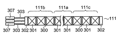
本発明に関わる磁界発生装置(以下コイル)111の概略を図6に示す。
【0049】
このコイル111は、例えば6個のボビン300に巻回され6分割されたコイル部301を有するセンターコイル111aと、このセンターコイル111aの両側に配置され、例えば夫々3個のボビン300に巻回され3分割されたコイル部301を有するサイドコイル111b、111cから構成されている。これら複数のボビン300を後述する単一のホルダーに順次嵌合させて、そのホルダーの両端部分をキャップ302等にて固定した一体構成を採っており、このキャップ302の一方側から各コイル部301の同種の引出線303が夫々束ねられて一括導出されている。
【0050】
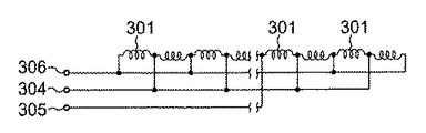
このコイル111の電気的な結線状態は、図7に示すように、各コイル部301の一端、即ち、例えば0V用の低圧側を共通端子304に、またセンターコイル111aのコイル部301の他方端となる例えば1000Vの高電位端となる端部を共通に接続して高圧側の第1の端子305に、両サイドコイル111b、111cの他方端となる例えば1000Vの高電位端を共通に接続して高圧側の第2の端子306に接続された構成となっている。
【0051】
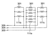
これを等価回路で示すと、図8に示すように、共通端子304と第1の端子305間にセンターコイル111aを構成する6個のコイル部301が並列に、また共通端子304と第2の端子306間に両サイドコイル111b、111cを構成する夫々3個のコイル部301が夫々並列となるように接続された回路となっている。
【0052】
実際の構成では、これらの各コイル部301の両端からの引出線303は全て各コイル部301毎に引出される構成となっており、共通端子304には12本、その他の第1及び第2の端子305,306には6本ずつの引出線303が導出されており、これを束ねて端子ピン(もしくは端子ソケット)307に接続されている。
【0053】
これらの各コイル部301は夫々非磁性材で絶縁物製の円筒状のボビン300に巻回されている。このボビン300は、図9に示すように、略円筒状に成形されたボビン本体308の内側に、内部に電線309を通すように空間を設けた枠状、例えば略コ字状の電線ガイド310が、その軸方向に形成されている。この電線ガイド310と対向するボビン本体308内側には、この電線ガイド310から見て左右対称となるように一対の枠状、例えばL字状の電線ガイド311が同様に軸方向に形成されている。
【0054】
このL字状の一対の電線ガイド311の中間、好ましくは中央部分のボビン本体308内壁面には、この内壁面よりも中心方向に放射状に突出したリブ312がボビン本体308の軸方向に形成され、更にコ字状の電線ガイド310の両側にも同様に一対のリブ312が形成されている。このリブ312は、ボビン300を一体成形するための金型構造の関係で、抜き方向にボビン本体308内面にテーパーを形成する必要から、ボビン本体308内壁面と後述するホルダー外壁面とを十分な面接触状態で嵌合位置固定することが困難なために、両者間の位置固定をするために必要としているものである。このために、正確な位置出しを行うためボビン本体308内側の円周上に3ケ所以上を必要とし、且つ、隣接するリブ312同士の中心との織り成す角度が180°未満となるように設定され、このリブ312の高さもボビン本体308最大内径部分に対して電線309径未満に設定される。このリブ312は、リブ312先端部分の面積がさほど大きくはないので、金型を抜く際の障害にはならない。
【0055】
このリブ312は、先端を平坦にせずに尖鋭にしたり、点もしくは線状に構成することも可能で、このように構成すると、ホルダー装着時により強い弾力性を発揮させることが可能となり、多少の成形上の誤差は吸収することが可能になるばかりでなく、この弾力性を利用して強固に固定させることも可能としている。
【0056】
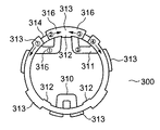
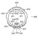
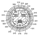
また、ボビン本体308外周面に電線309を巻回する際に、この電線309がボビン本体308から脱落しないようにボビン本体308の両端部には、外周方向に所定の間隔を隔てて放射状に展開する複数のフランジ313が形成される。このフランジ313は、ボビン本体308を一方側から見た図10、及び他方側から見た図11に示すように、一端面側及び他方端面側から見た場合に、夫々の端部に形成したフランジ313が互いに透視できるように、夫々が重ならない位置に形成されている。このようなフランジ313の配置は、ボビン300成形時の金型の抜き方向の問題を解消するための工夫である。
【0057】
このフランジ313は、片側で最低1ケ所以上に配置され、フランジ313が1個で形成される場合には、このフランジ313を設けていない空隙部分が180°未満の大きさとなるようにフランジ313の外周面方向の長さを設定し、巻回された電線309がボビン本体308外周から外れないように考慮する必要がある。また、このフランジ313を外周方向に複数個配置する場合には、所定の間隔で配置するとともに、ボビン本体308の両端に形成されるフランジ313同士が軸方向に対して重ならない位置にずらして配設することにより、金型をボビン300の軸方向に型抜きできるように構成することで、金型の構造の簡略化を図り、且つ金型の製造コストの低減化を可能にしている。
【0058】
このフランジ313の中間部分のボビン本体308端面には、ボビン本体308の内外側面を連結するように放射方向に溝部314が設けられ、この溝部314は一方端面ではL字型の電線ガイド311に夫々対向する位置に、また他方端面にはコ字状の電線ガイド310に対向する位置に設けられている。換言すれば、溝部314の両側に夫々フランジ313を設けた構成となっている。この溝部314はボビン本体308外周面に電線309を巻回した際に、その電線309の巻き始め及び巻き終わりの引出線315部分を、そのボビン本体308からの導出方向側の引出線315を溝部314を通して内側に、導出方向と反対側の引出線315は、溝部314及び電線ガイド310を通して同じ導出方向に引出すようにしているものである。
【0059】
この溝部314は隣接するボビン本体308同士を当接させた際に、ボビン本体308の内側に引き込まれる電線309がボビン本体308間に挟み込まれるのを防止するとともに、溝部314の両側に形成しているフランジ313が電線309のガイドとしての機能を果たすことから、巻線作業の効率化及び巻線完成時の電線309の抜け止めとしての役目も受け持っている。この溝部314が形成される位置は、そこから電線309が挿入されるボビン本体308内部の空間に対して±90°以下の位置に設けると、電線309が通過する空隙部分に有効に電線309を導くことができるので、±90°以内に形成するのが好ましい。
【0060】
また、上述のように電線309の巻回方向に2種類の巻き方が存在し、しかも電線309の引出線315導出方向が一方向に設定されているので、この巻方向及び引出方向を区別するために、ボビン本体308の2つの溝部314が形成されている一端面側側面に、L字状の電線ガイド311の各溝部314の両側に電線309の巻回方向を示す矢印及び数字の符号316を一体成形もしくは印刷等で形成し、更に電線ガイド311に所要の電線309の引出線315を通すための区分用の数字からなる符号316が形成されている。一方、ボビン本体308の他方端面側には、溝部314の両側側面に同様にして矢印と数字の符号316が一体成形もしくは印刷等で形成され、コ字状の電線ガイド310の端面にも数字からなる符号316が形成されている。
【0061】
これらの矢印及び数字等の符号316は、例えば図10に図示されている端面側の数字▲1▼を例にとって説明すると、この数字▲1▼側の電線309は高圧側に位置する電線309端部でL字状の電線ガイド311に一端を挿入し、溝部314を通して矢印方向に右巻きに奥に向かって巻回していくことを表しており、この電線309の終端は図11の溝部314から図中手前側に導出される。また仮に図10の数字▲2▼の場合には、一端を図中手前側に位置させて溝部314から左巻きに巻回してゆき、終端を図11の溝部314を介してコ字状の電線ガイド310を通して反対他面側(図10端面方向)に導出するもので、図10に示している端面方向に電線309の引出線315が導出されることを表している。
【0062】
このように、矢印及び数字等の符号316によって巻き始め及び巻き終わり位置並びに巻回方向を指示しており、コイル部301の製造段階での組立ミスの防止を図っているもので、個別にコイル部301が完成された場合でも容易に設計通りに組立られているかの確認も行うことができ、欠品の抑制を図ることができる。
【0063】
この矢印及び数字等の符号316は、例えば矢印をフランジ313の溝部314の部分を三角状に欠いた形状にして方向を示すような形状とすることで方向を表示することでも可能であり、また数字に代えて数に応じた突起や三角、四角等の図形表示等とすることも可能であり、これらを機能的に組合せて使用することも可能である。
【0064】
なお、この符号316は、フランジ313面に形成すると容易に挿入されるべき電線309の種別や巻回方向の判定が容易に行えるが、電線309を巻回するボビン本体308外周面の端部に形成したり、ボビン本体308の端面に直接形成することも可能である。
【0065】
このように構成されたボビン300は、夫々の端面方向から見た場合に、夫々の端面は軸を中心として対称な形状を呈しているので、このボビン300を前後反転させて使用してもホルダーに装着可能であり、例えば巻回方向を逆に巻回する場合、あるいは同電位部分を対向させてボビン300をホルダー上に順次嵌合させる場合においても、同じ形状のボビン300をそのまま使用することが可能なので、少ない種類のボビン300を用意するだけで事足り、量産が可能となっている。
【0066】
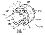
このようにボビン本体308外周面に電線309を巻回し、その引出線315部分を同一方向となるように構成された夫々のコイル部301は、軸方向に細長いホルダーの外周上に順次嵌合装着されてコイル111を構成している。
【0067】
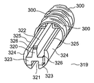
このホルダー319は、図12に示すように、中心部に断面略凸字状で中央突出部320に対向する底部にボビン本体308に設けた電線ガイド310を嵌合し、且つこの電線ガイド310の高さよりも深い凹部321を形成したテトラポット状の芯体部322を有し、更にこの凹部321の両側の凸部323側面に連接し中央突出部320と離間して配置される外側面を湾曲させた扇状の側壁部324を一体に設けた構成になっている。そしてボビン本体308を嵌合した際に、ボビン本体308内のL字状の電線ガイド311が当接しないように側壁部324の一部を切り欠いて逃げ用の平坦部325を形成している。そして、この芯体部322の両端外周部分、あるいは側壁部324の外周には、コイル本体308をホルダー319上に固定するためのキャップ302嵌め込み用の螺子溝326が設けられている。
【0068】
このホルダー319に図6にも示しているように、電線309が巻回された12個のボビン300を順次嵌合させて両端をキャップ302にて固定させているが、これらボビン300は前述の通り交互に巻線方向が反転するように巻回させたコイル部301を有するボビン300を順次配置させており、且つコイル部301に流れる電流方向は全て同じ方向となるように構成している。従って電線309の巻回方向としては2種類の巻き方が存在するので、この巻回方向を区別するために、例えば右巻きの場合には、図10中の左側の溝部314を利用し、反対に左巻きの場合には右側の溝部314を利用するように構成する。
【0069】
このようにホルダー319に順次電線309を巻回したボビン300を装着していくと、ボビン300内径部とホルダー319外側面との隙間は、リブ312の高さを電線309径未満に設定しているために、ボビン300をホルダー319に嵌合する際に電線309をボビン本体308とホルダー319間に挟み込むこともない。このホルダー319にボビン本体308を嵌合した際に、図13に示すように、ホルダー319とボビン300との間に左右電線ガイド311の下側及びコ字状電線ガイド310の上側に夫々軸方向に連なる空隙部330を形成している。この空隙部330には、自身に電線309を巻回したボビン300以外の順次連接されている他のボビン300に巻回された電線309の引出線315が配置されて同一方向に導出されている。例えば図中左側の空隙部330には、図7に示す第1の端子305に接続される引出線315群が、右側の空隙部330には同じく第2の端子306に接続される引出線315群が、また下側の空隙部330には共通端子304に接続される引出線315群が夫々配置されるようにしている。
【0070】
このようにボビン300とホルダー319とを同軸になるように配置させることで、コイル部301の組立てを精度よく効率的に組立てることができ、しかも誤差を低減する構成とすることが可能である。また、ホルダー319の外周面上に夫々電線309を巻回したボビン300を嵌合してコイル111とし、このコイル111全体を耐熱性の絶縁筒331で覆ってヒートローラ101中に装着して定着装置を構成している。この耐熱性絶縁筒331は、電線309とヒートローラ101間の耐絶縁性を向上させるためのもので、電線309に傷がついて絶縁性が劣化したとしても、この電線309とヒートローラ101間で放電等の不測の事態が発生しないように予防するために装着しているもので、十分な耐絶縁性が保持し得るのであれば省略することも可能である。このようにして、ホルダー319とボビン300とが同軸的に配置され、しかも各コイル部301とヒートローラ101間の距離を略一定に保つことができるので、ヒートローラ101の温度ムラを低減することが可能となっている。
【0071】
【発明の効果】
以上述べたようにこの発明によれば、各種紙サイズによる定着性不具合のない実用性および信頼性にすぐれ、且つ製造が容易で作業性に富んだ誘導加熱用の磁界発生装置およびそれを用いた定着装置を提供できる。
【図面の簡単な説明】
【図1】実施形態の内部の構成を示す図。
【図2】実施形態における定着装置の構成を示す図。
【図3】実施形態の電子複写機の制御回路を示すブロック図。
【図4】実施形態の定着装置における電気回路の構成図。
【図5】実施形態の定着装置における各直列共振回路の出力電力とその各直列共振回路を励起する周波数との関係を示す図。
【図6】磁界発生装置(コイル)111の概略を示す図。
【図7】磁界発生装置の電気回路の構成図。
【図8】磁界発生装置の等価回路の構成図。
【図9】磁界発生装置を構成するボビンを示す斜視図。
【図10】同じくボビンを一端面側から見た平面図。
【図11】同じくボビンを他端面側から見た平面図。
【図12】磁界発生装置を構成するホルダーを示す斜視図。
【図13】実施形態における定着装置の具体的な構成を示す図。
【符号の説明】
1…本体、20…感光体ドラム、100…定着装置、101…加熱ローラ、102…加圧ローラ、111a,111b,111c…コイル、120…高周波発生回路、121…整流回路、122…スイッチング回路、123,124,125…コンデンサ、126…トランジスタ(スイッチング素子)、140…コントローラ、141…発振回路、142…CPU、150…電流検知回路、171…コイル、300…ボビン、301…コイル部、308…ボビン本体、309…電線、310…電線ガイド、311…電線ガイド、312…リブ、313…フランジ、314…溝部、315…引出線、316…符号[0001]
BACKGROUND OF THE INVENTION
The present invention relates to a fixing device that is mounted on an image forming apparatus such as a copying machine or a printer and fixes a developer image on a sheet.
[0002]
[Prior art]
In an image forming apparatus using digital technology such as an electronic copying machine, a document table on which a document is placed is exposed, and reflected light from the document table is guided to a photoelectric conversion element such as a CCD (charge coupled device).
[0003]
The CCD outputs an image signal corresponding to the original image. Laser light corresponding to the image signal is irradiated onto the photosensitive drum, and an electrostatic latent image is formed on the peripheral surface of the photosensitive drum. This electrostatic latent image is visualized by the adhesion of developer (toner). A sheet is fed to the photosensitive drum in synchronization with the rotation of the photosensitive drum, and a visible image (developer image) on the photosensitive drum is transferred to the sheet. The sheet on which the developer image is transferred is sent to a fixing device.
[0004]
The fixing device includes a heating roller and a pressure roller that rotates with the heating roller while being in contact with the heating roller in a pressurized state. The developer image on the paper is fixed by heat.
[0005]
There is induction heating as a heat source of the heating roller. This is because a coil is placed in a heating roller, a capacitor is connected to the coil to form a resonance circuit, and the resonance circuit is excited at one frequency with respect to one resonance circuit, whereby a high-frequency current is passed through the coil. A high frequency magnetic field is generated from the coil, an eddy current is generated in the heating roller by the high frequency magnetic field, and the heating roller self-heats by Joule heat generated by the eddy current.
[0006]
This fixing device using induction heating heats a fixing roller made of a metal conductor by eddy current due to electromagnetic waves, and an induction coil spirally wound around a non-magnetic bobbin is provided in the fixing roller. By causing a high-frequency current to flow through the induction coil, an induced eddy current is generated in the fixing roller by a high-frequency magnetic field generated thereby, and the fixing roller itself is heated by Joule heat by the skin resistance of the fixing roller. This bobbin is divided into three parts: a central main bobbin member and a slave bobbin member connected to both sides of the bobbin member for the purpose of easy manufacture and repair, and a conductive wire is wound around each of the divided bobbin members. Thus, an induction coil is configured (see, for example, Patent Document 1).
[0007]
[Patent Document 1]
Japanese Patent Laying-Open No. 2001-312165 (page 2-3, FIG. 1)
[0008]
[Problems to be solved by the invention]
In recent years, shortening W / U has become a technical issue as an energy-saving technology, but as a countermeasure, the heating roller can be made thinner. However, since various types of paper sizes are used in the fixing device, when the narrow paper is continuously passed, the outside of the paper on the heating roller is not deprived of heat by the paper. The phenomenon that fixing failure due to high temperature offset occurs when a wide sheet is passed after a narrow sheet becomes high due to the fact that the heating roller is thick. The thinner (the smaller the heat capacity), the more prominent.
[0009]
Further, in manufacturing the coil constituting the fixing device, further efficiency and ease of manufacturing have been demanded.
[0010]
The present invention has been made in consideration of the above circumstances, and an object of the present invention is to provide an induction heating fixing device excellent in practicality and reliability that can solve the above-described problems.
[0011]
[Means for Solving the Problems]
As a means for solving the above-mentioned problems, the present invention comprises a member to be heated that generates heat due to the generation of eddy currents, and a wire wound around the main body a plurality of times, and leads the input side and output side of the wire to both ends, respectively. A bobbin having a groove, a holder for supporting a plurality of the bobbins, and an electric wire arranged inside the bobbin, drawn out from the main body, passed through the groove, and guided toward the end of the holder The direction of the bobbin with reference to the code that has a guide, is written on the main body and identifies the wire in the groove, and the code that is written on the wire guide and identifies the wire in the wire guide A plurality of coil units assembled by inserting a plurality of the holders into the holder are arranged adjacent to the member to be heated, and the eddy current is generated in the member to be heated. And the coil unit group, wherein with a predetermined pressure the recording medium in contact with the member to be heated, wherein those comprising a pressure member for clamping conveyed with heated member.
[0012]
DETAILED DESCRIPTION OF THE INVENTION
Embodiments of the present invention will be described below with reference to the drawings.
[0013]
First, FIG. 1 shows an internal configuration of an image forming apparatus such as a composite electronic copying machine. A transparent document table (glass plate) 2 for placing a document is provided on the upper surface of the
[0014]
The reflected light by this exposure is projected onto a photoelectric conversion element such as a CCD (Charge Coupled Device) 10 to output an image signal. The image signal output from the
[0015]
Although not shown, a control panel for setting operating conditions is provided on the upper surface of the
[0016]
On the other hand, a
[0017]
A specific configuration of the
[0018]
A
[0019]
The
[0020]
Around the
[0021]
Inside the
[0022]
A control circuit of the
[0023]
A scan CPU 70, a
[0024]
Further, a
[0025]
The network interface 59 functions as an input unit for a printer mode to which an image (image data) transmitted from an external device is input. A
[0026]
The FAX transmission /
[0027]
A ROM 71 for storing a control program, a RAM 72 for storing data, a
[0028]
Connected to the
[0029]
A
[0030]
A print unit that prints the image processed by the image processing unit 55 on the paper P is mainly configured by the
[0031]
An electric circuit of the fixing
[0032]
The
[0033]
A
[0034]
The high
[0035]
The first series resonance circuit has a resonance frequency f1 determined by the inductance L1 of the
[0036]
The
[0037]
(1) When the operation of the first series resonance circuit (using only the
[0038]
(2) When the operation of the first and second series resonant circuits (use of all the
[0039]
Next, the operation of the above configuration will be described.
[0040]
When a drive signal having the same frequency (or a nearby frequency) as the resonance frequency f1 of the first series resonance circuit is emitted from the
[0041]
When a drive signal having the same frequency (or a nearby frequency) as the resonance frequency f2 of the second series resonance circuit is emitted from the
[0042]
The relationship between the output power P1 of the first series resonance circuit and the frequency for exciting the first series resonance circuit, and the relationship between the output power P2 of the second series resonance circuit and the frequency for exciting the second series resonance circuit are shown. This is shown in FIG.
[0043]
That is, the output power P1 of the first series resonance circuit becomes a peak level when excited at the same frequency as the resonance frequency f1 of the first series resonance circuit, and becomes a peak as the excited frequency goes away from the resonance frequency f1. The pattern gradually decreases. Similarly, the output power P2 of the second series resonance circuit becomes a peak level when excited at the same frequency as the resonance frequency f2 of the second series resonance circuit, and becomes a peak as the excited frequency goes away from the resonance frequency f2. The pattern gradually decreases.
[0044]
When fixing a large size paper S, both the first and second series resonance circuits are excited, and high frequency magnetic fields are emitted from all the
[0045]
In this case, drive signals having two frequencies (f1−Δf) and (f1 + Δf) that are separated by a predetermined value Δf in the vertical direction around the resonance frequency f1 of the first series resonance circuit are sequentially output from the
[0046]
By these drive signals, the first series resonance circuit is sequentially excited at two frequencies (f1−Δf) and (f1 + Δf) sandwiching the resonance frequency f1, and then, the second series resonance circuit has its resonance frequency f2. Are sequentially excited at two frequencies (f2−Δf) and (f2 + Δf). The excitation for each frequency is repeated.
[0047]
As shown in FIG. 5, the output power P1 of the
[0048]
An outline of a magnetic field generator (hereinafter referred to as a coil) 111 according to the present invention is shown in FIG.
[0049]
For example, the
[0050]
As shown in FIG. 7, this
[0051]
When this is shown by an equivalent circuit, as shown in FIG. 8, the six
[0052]
In an actual configuration, all of the
[0053]
Each of these
[0054]
On the inner wall surface of the bobbin
[0055]
The
[0056]
Further, when the
[0057]
The
[0058]
A
[0059]
The
[0060]
Also, as described above, there are two types of winding methods in the winding direction of the
[0061]
These
[0062]
In this way, the winding start and winding end positions and the winding direction are indicated by
[0063]
For example, the
[0064]
In addition, although this code |
[0065]
When the
[0066]
In this way, each
[0067]
As shown in FIG. 12, the
[0068]
As shown in FIG. 6, twelve
[0069]
When the
[0070]
Thus, by arranging the
[0071]
【The invention's effect】
As described above, according to the present invention, a magnetic field generator for induction heating, which is excellent in practicality and reliability free from fixing problems due to various paper sizes, is easy to manufacture and has high workability, and the same are used. A fixing device can be provided.
[Brief description of the drawings]
FIG. 1 is a diagram showing an internal configuration of an embodiment.
FIG. 2 is a diagram illustrating a configuration of a fixing device in the embodiment.
FIG. 3 is a block diagram illustrating a control circuit of the electronic copying machine according to the embodiment.
FIG. 4 is a configuration diagram of an electric circuit in the fixing device according to the embodiment.
FIG. 5 is a diagram illustrating a relationship between output power of each series resonance circuit and a frequency for exciting each series resonance circuit in the fixing device according to the embodiment.
6 is a diagram showing an outline of a magnetic field generator (coil) 111. FIG.
FIG. 7 is a configuration diagram of an electric circuit of the magnetic field generator.
FIG. 8 is a configuration diagram of an equivalent circuit of the magnetic field generator.
FIG. 9 is a perspective view showing a bobbin constituting the magnetic field generator.
FIG. 10 is a plan view of the bobbin as seen from one end surface side.
FIG. 11 is a plan view of the bobbin as seen from the other end surface side.
FIG. 12 is a perspective view showing a holder constituting the magnetic field generator.
FIG. 13 is a diagram illustrating a specific configuration of the fixing device according to the embodiment.
[Explanation of symbols]
DESCRIPTION OF
Claims (4)
本体に電線を複数回巻きつけてなり、両端部に前記電線の入力側と出力側を夫々導く溝部を有するボビン、及び前記ボビンを複数個支持するホルダ、並びに前記ボビンの内側に配置され前記本体から引き出されて前記溝部を経た前記電線を通過させて、前記ホルダの端部方向に導く電線ガイドを有し、前記本体に表記され、前記溝部にある前記電線を識別する符号、及び前記電線ガイドに表記され、前記電線ガイドにある前記電線を識別する符号を参照して、前記ボビンの方向を定めて前記ホルダに複数個挿通することにより組み立てられるコイルユニットを、前記被加熱部材に複数個隣接配置してなり、前記被加熱部材に前記渦電流を発生させるコイルユニット群と、
前記被加熱部材に接触して記録媒体を所定の圧力を持って、前記被加熱部材と共に挟持搬送する加圧部材とを有することを特徴とする誘導加熱定着装置。A heated member that generates heat due to the generation of eddy current;
A bobbin formed by winding a wire around the main body a plurality of times and having groove portions for guiding the input side and the output side of the electric wire at both ends, a holder for supporting a plurality of bobbins, and the main body disposed inside the bobbin A wire guide that passes through the groove drawn through the groove and leads in the direction of the end of the holder, a code that is written on the body and identifies the wire in the groove, and the wire guide And a plurality of coil units assembled by inserting a plurality of the holders in the direction of the bobbin with reference to the reference numerals for identifying the wires in the wire guide. A coil unit group configured to generate the eddy current in the heated member;
An induction heating fixing apparatus, comprising: a pressure member that contacts the heated member and holds and conveys the recording medium together with the heated member with a predetermined pressure.
本体に電線を複数回巻きつけてなり、両端部に前記電線の入力側と出力側を夫々導く溝部を有するボビン、及び前記ボビンを複数個支持するホルダ、並びに前記ボビンの内側に配置され前記本体から引き出されて前記溝部を経た前記電線を通過させて、前記ホルダの端部方向に導く電線ガイドを有し、前記本体に表記され、前記溝部にある前記電線を識別する符号、及び前記電線ガイドに表記され、前記電線ガイドにある前記電線を識別する符号を参照して、前記ボビンの方向を定めて前記ホルダに複数個挿通することにより組み立てられるコイルユニットと、 A bobbin formed by winding a wire around the main body a plurality of times and having groove portions for guiding the input side and the output side of the wire at both ends, a holder for supporting a plurality of bobbins, and the main body disposed inside the bobbin A wire guide that passes through the groove portion drawn through the groove portion and guides the wire toward the end of the holder, a code that is written on the body and identifies the wire in the groove portion, and the wire guide A coil unit that is assembled by referring to a code that identifies the electric wire in the electric wire guide and by inserting a plurality of the bobbin into the holder,
コイル巻き方向の異なる複数種類の前記コイルユニットを前記被加熱部材に複数個隣接配置してなり、前記被加熱部材に前記渦電流を発生させるコイルユニット群と、A plurality of types of the coil units having different coil winding directions are arranged adjacent to the heated member, and a coil unit group for generating the eddy current in the heated member;
前記被加熱部材に接触して記録媒体を所定の圧力を持って、前記被加熱部材と共に挟持搬送する加圧部材とを有することを特徴とする誘導加熱定着装置。 An induction heating fixing device comprising: a pressure member that contacts the heated member and holds and conveys the recording medium together with the heated member with a predetermined pressure.
Priority Applications (3)
| Application Number | Priority Date | Filing Date | Title |
|---|---|---|---|
| JP2003085900A JP3917543B2 (en) | 2003-03-26 | 2003-03-26 | Induction heating fixing device |
| US10/807,366 US6861627B2 (en) | 2003-03-26 | 2004-03-24 | Induction heat fixing device |
| US10/943,979 US7161123B2 (en) | 2003-03-26 | 2004-09-20 | Induction heat fixing device |
Applications Claiming Priority (1)
| Application Number | Priority Date | Filing Date | Title |
|---|---|---|---|
| JP2003085900A JP3917543B2 (en) | 2003-03-26 | 2003-03-26 | Induction heating fixing device |
Publications (2)
| Publication Number | Publication Date |
|---|---|
| JP2004294692A JP2004294692A (en) | 2004-10-21 |
| JP3917543B2 true JP3917543B2 (en) | 2007-05-23 |
Family
ID=33400690
Family Applications (1)
| Application Number | Title | Priority Date | Filing Date |
|---|---|---|---|
| JP2003085900A Expired - Fee Related JP3917543B2 (en) | 2003-03-26 | 2003-03-26 | Induction heating fixing device |
Country Status (1)
| Country | Link |
|---|---|
| JP (1) | JP3917543B2 (en) |
-
2003
- 2003-03-26 JP JP2003085900A patent/JP3917543B2/en not_active Expired - Fee Related
Also Published As
| Publication number | Publication date |
|---|---|
| JP2004294692A (en) | 2004-10-21 |
Similar Documents
| Publication | Publication Date | Title |
|---|---|---|
| US20060086726A1 (en) | Heating apparatus and image forming apparatus | |
| US6954608B2 (en) | Heating device and image forming apparatus | |
| US6861627B2 (en) | Induction heat fixing device | |
| EP1700171A1 (en) | Heating apparatus | |
| US7105783B2 (en) | Fixing device using induction heating | |
| JP3655262B2 (en) | Fixing device | |
| JP3917543B2 (en) | Induction heating fixing device | |
| JP3842234B2 (en) | Induction heating fixing device | |
| JP3854091B2 (en) | Fixing device | |
| JP2004294693A (en) | Induction heating fixing device | |
| JP4873532B2 (en) | Fixing apparatus and image forming apparatus | |
| US7171149B2 (en) | Fixing apparatus | |
| JP3853750B2 (en) | Fixing device | |
| JP2004294489A (en) | Fixing device | |
| JP5016388B2 (en) | Fixing apparatus and image forming apparatus | |
| JP4832188B2 (en) | Fixing apparatus and image forming apparatus | |
| JP3843076B2 (en) | Fixing device | |
| JP2004287247A (en) | Fixing device | |
| JP5451413B2 (en) | Image heating device | |
| JP2004294548A (en) | Fixing device | |
| JP4296984B2 (en) | Fixing apparatus and image forming apparatus | |
| JP2004294487A (en) | Fixing device | |
| JP2004294488A (en) | Fixing device | |
| JP2004287245A (en) | Fixing device | |
| JP2004294549A (en) | Fixing device |
Legal Events
| Date | Code | Title | Description |
|---|---|---|---|
| A621 | Written request for application examination |
Free format text: JAPANESE INTERMEDIATE CODE: A621 Effective date: 20060116 |
|
| RD04 | Notification of resignation of power of attorney |
Free format text: JAPANESE INTERMEDIATE CODE: A7424 Effective date: 20060119 |
|
| RD02 | Notification of acceptance of power of attorney |
Free format text: JAPANESE INTERMEDIATE CODE: A7422 Effective date: 20060707 |
|
| A977 | Report on retrieval |
Free format text: JAPANESE INTERMEDIATE CODE: A971007 Effective date: 20060830 |
|
| A131 | Notification of reasons for refusal |
Free format text: JAPANESE INTERMEDIATE CODE: A131 Effective date: 20060905 |
|
| A521 | Written amendment |
Free format text: JAPANESE INTERMEDIATE CODE: A523 Effective date: 20061102 |
|
| A131 | Notification of reasons for refusal |
Free format text: JAPANESE INTERMEDIATE CODE: A131 Effective date: 20061121 |
|
| A521 | Written amendment |
Free format text: JAPANESE INTERMEDIATE CODE: A523 Effective date: 20070117 |
|
| TRDD | Decision of grant or rejection written | ||
| A01 | Written decision to grant a patent or to grant a registration (utility model) |
Free format text: JAPANESE INTERMEDIATE CODE: A01 Effective date: 20070206 |
|
| A61 | First payment of annual fees (during grant procedure) |
Free format text: JAPANESE INTERMEDIATE CODE: A61 Effective date: 20070208 |
|
| R150 | Certificate of patent or registration of utility model |
Ref document number: 3917543 Country of ref document: JP Free format text: JAPANESE INTERMEDIATE CODE: R150 Free format text: JAPANESE INTERMEDIATE CODE: R150 |
|
| FPAY | Renewal fee payment (event date is renewal date of database) |
Free format text: PAYMENT UNTIL: 20100216 Year of fee payment: 3 |
|
| FPAY | Renewal fee payment (event date is renewal date of database) |
Free format text: PAYMENT UNTIL: 20110216 Year of fee payment: 4 |
|
| FPAY | Renewal fee payment (event date is renewal date of database) |
Free format text: PAYMENT UNTIL: 20110216 Year of fee payment: 4 |
|
| FPAY | Renewal fee payment (event date is renewal date of database) |
Free format text: PAYMENT UNTIL: 20120216 Year of fee payment: 5 |
|
| FPAY | Renewal fee payment (event date is renewal date of database) |
Free format text: PAYMENT UNTIL: 20120216 Year of fee payment: 5 |
|
| FPAY | Renewal fee payment (event date is renewal date of database) |
Free format text: PAYMENT UNTIL: 20130216 Year of fee payment: 6 |
|
| FPAY | Renewal fee payment (event date is renewal date of database) |
Free format text: PAYMENT UNTIL: 20130216 Year of fee payment: 6 |
|
| FPAY | Renewal fee payment (event date is renewal date of database) |
Free format text: PAYMENT UNTIL: 20140216 Year of fee payment: 7 |
|
| LAPS | Cancellation because of no payment of annual fees |