JP3911195B2 - Optical disc recording method and apparatus - Google Patents
Optical disc recording method and apparatus Download PDFInfo
- Publication number
- JP3911195B2 JP3911195B2 JP2002136983A JP2002136983A JP3911195B2 JP 3911195 B2 JP3911195 B2 JP 3911195B2 JP 2002136983 A JP2002136983 A JP 2002136983A JP 2002136983 A JP2002136983 A JP 2002136983A JP 3911195 B2 JP3911195 B2 JP 3911195B2
- Authority
- JP
- Japan
- Prior art keywords
- signal
- auxiliary
- recording
- clock
- optical disc
- Prior art date
- Legal status (The legal status is an assumption and is not a legal conclusion. Google has not performed a legal analysis and makes no representation as to the accuracy of the status listed.)
- Expired - Lifetime
Links
- 230000003287 optical effect Effects 0.000 title claims description 146
- 238000000034 method Methods 0.000 title claims description 30
- 230000006641 stabilisation Effects 0.000 claims description 93
- 238000011105 stabilization Methods 0.000 claims description 93
- 238000001514 detection method Methods 0.000 claims description 11
- 230000001360 synchronised effect Effects 0.000 claims description 9
- 230000003044 adaptive effect Effects 0.000 description 28
- 238000010586 diagram Methods 0.000 description 21
- 230000005540 biological transmission Effects 0.000 description 13
- 230000010365 information processing Effects 0.000 description 9
- 230000000630 rising effect Effects 0.000 description 9
- 230000007423 decrease Effects 0.000 description 8
- 101000904787 Homo sapiens Serine/threonine-protein kinase ATR Proteins 0.000 description 2
- 201000006783 Seckel syndrome Diseases 0.000 description 2
- 102100023921 Serine/threonine-protein kinase ATR Human genes 0.000 description 2
- 201000009310 astigmatism Diseases 0.000 description 1
- 230000003247 decreasing effect Effects 0.000 description 1
- 230000000694 effects Effects 0.000 description 1
- 230000010355 oscillation Effects 0.000 description 1
Images


Classifications
-
- G—PHYSICS
- G11—INFORMATION STORAGE
- G11B—INFORMATION STORAGE BASED ON RELATIVE MOVEMENT BETWEEN RECORD CARRIER AND TRANSDUCER
- G11B20/00—Signal processing not specific to the method of recording or reproducing; Circuits therefor
- G11B20/10—Digital recording or reproducing
- G11B20/12—Formatting, e.g. arrangement of data block or words on the record carriers
-
- H—ELECTRICITY
- H03—ELECTRONIC CIRCUITRY
- H03L—AUTOMATIC CONTROL, STARTING, SYNCHRONISATION OR STABILISATION OF GENERATORS OF ELECTRONIC OSCILLATIONS OR PULSES
- H03L7/00—Automatic control of frequency or phase; Synchronisation
- H03L7/06—Automatic control of frequency or phase; Synchronisation using a reference signal applied to a frequency- or phase-locked loop
- H03L7/16—Indirect frequency synthesis, i.e. generating a desired one of a number of predetermined frequencies using a frequency- or phase-locked loop
- H03L7/18—Indirect frequency synthesis, i.e. generating a desired one of a number of predetermined frequencies using a frequency- or phase-locked loop using a frequency divider or counter in the loop
-
- G—PHYSICS
- G11—INFORMATION STORAGE
- G11B—INFORMATION STORAGE BASED ON RELATIVE MOVEMENT BETWEEN RECORD CARRIER AND TRANSDUCER
- G11B20/00—Signal processing not specific to the method of recording or reproducing; Circuits therefor
- G11B20/10—Digital recording or reproducing
- G11B20/14—Digital recording or reproducing using self-clocking codes
- G11B20/1403—Digital recording or reproducing using self-clocking codes characterised by the use of two levels
-
- G—PHYSICS
- G11—INFORMATION STORAGE
- G11B—INFORMATION STORAGE BASED ON RELATIVE MOVEMENT BETWEEN RECORD CARRIER AND TRANSDUCER
- G11B27/00—Editing; Indexing; Addressing; Timing or synchronising; Monitoring; Measuring tape travel
- G11B27/10—Indexing; Addressing; Timing or synchronising; Measuring tape travel
- G11B27/19—Indexing; Addressing; Timing or synchronising; Measuring tape travel by using information detectable on the record carrier
- G11B27/28—Indexing; Addressing; Timing or synchronising; Measuring tape travel by using information detectable on the record carrier by using information signals recorded by the same method as the main recording
- G11B27/30—Indexing; Addressing; Timing or synchronising; Measuring tape travel by using information detectable on the record carrier by using information signals recorded by the same method as the main recording on the same track as the main recording
- G11B27/3027—Indexing; Addressing; Timing or synchronising; Measuring tape travel by using information detectable on the record carrier by using information signals recorded by the same method as the main recording on the same track as the main recording used signal is digitally coded
-
- H—ELECTRICITY
- H03—ELECTRONIC CIRCUITRY
- H03L—AUTOMATIC CONTROL, STARTING, SYNCHRONISATION OR STABILISATION OF GENERATORS OF ELECTRONIC OSCILLATIONS OR PULSES
- H03L7/00—Automatic control of frequency or phase; Synchronisation
- H03L7/06—Automatic control of frequency or phase; Synchronisation using a reference signal applied to a frequency- or phase-locked loop
- H03L7/08—Details of the phase-locked loop
- H03L7/085—Details of the phase-locked loop concerning mainly the frequency- or phase-detection arrangement including the filtering or amplification of its output signal
- H03L7/087—Details of the phase-locked loop concerning mainly the frequency- or phase-detection arrangement including the filtering or amplification of its output signal using at least two phase detectors or a frequency and phase detector in the loop
-
- G—PHYSICS
- G11—INFORMATION STORAGE
- G11B—INFORMATION STORAGE BASED ON RELATIVE MOVEMENT BETWEEN RECORD CARRIER AND TRANSDUCER
- G11B2220/00—Record carriers by type
- G11B2220/20—Disc-shaped record carriers
Landscapes
- Engineering & Computer Science (AREA)
- Signal Processing (AREA)
- Optical Recording Or Reproduction (AREA)
- Signal Processing For Digital Recording And Reproducing (AREA)
Description
【0001】
【発明の属する技術分野】
本発明は、信号トラックの物理的位置を指示する補助信号が信号トラックとは異なる領域にプリフォーマットされた光ディスクに情報を記録する技術に関し、特に信号トラック上の不連続記録位置に情報を記録する光ディスク記録方法及び装置に関する。
【0002】
【従来の技術】
通常のコンパクトディスク(以下CDと言う)及びデジタルバーセタイルディスク(Digital Versatile Disc,以下“DVD”と言う)のような光ディスクには情報が記録される信号トラックが螺旋形又は同心円の形態に形成されている。又、光ディスクには信号トラックがランダムにアクセスすることができるように補助信号がプリフォーマットされていた。この補助信号は、信号トラックを一定の大きさの単位格納領域に区分し、これらの単位格納領域の物理的位置を指示する。
【0003】
補助信号は、ハードセクター方式とソフトセクター方式の二つ方式で光ディスクにプリフォーマットされている。前者のハードセクター方式によると、光ディスクの信号トラックの一部領域にエンボスピット(Embossed Pit)を形成することによって補助信号が光ディスクにプリフォーマットされるようになる。このように、補助信号がプリフォーマットされた光ディスク(10)には、図1に示したように同心円又は螺旋形の信号トラック(12)が一定の長さのセクター(14)に区分される。これらのセクター(14)の各々は、セクター識別信号部(16)とメイン情報信号部(18)で構成される。セクター識別信号部(16)は同期パターン、アドレスマーク、トラック番号及びセクター番号を含み、隣接したセクターとの境界部を指示すると共に、そのセクターの物理的位置を指示する補助信号に使用される。メイン情報信号部(18)にはユーザー情報が記録される。このような、ハードセクター方式の補助信号はユーザー情報が記録される信号トラックの一部区間を占有するので光ディスクの記録容量を少なくさせる。
【0004】
後者のソフトセクター方式の補助信号は、光ディスクの信号トラックとは他の別の領域、ウォッブル領域に配置することによって光ディスクの記録領域を大きくすることができる。このソフトセクター方式に補助信号がプリフォーマットされた光ディスクには、図2に示すように光ディスクの中心から外周まで螺旋形又は同心円の形態に形成された溝(22)(以下、溝のトラックと言う)が一定サイクルで曲がっており、これらの溝のトラック(22)間には、ランド(20)(以下、山のトラックと言う)が配列されている。補助信号は、溝のトラック(22)両側辺の曲がった部分(以下、“ウォッブル領域”と言う)に補助信号がプリフォーマットされている。
【0005】
このような、ソフトセクター方式の補助信号がプリフォーマットされた光ディスクの信号トラックに記録されるユーザー情報ブロックは、ユーザーブロック識別部とユーザーブロック情報部で構成される。このユーザーブロック識別部は、ハードセクター方式の補助信号と同じように同期パターン、アドレスマーク、トラック番号及びブロック番号等を含む。このように構成されたユーザーブロック識別部は再生の時、光ディスクの信号トラックの物理的位置を指示するようになる。従って、ソフトセクター方式の補助信号はユーザー情報を光ディスクに記録する場合に主として使用する。
【0006】
又、補助信号はユーザー情報の伝送速度、即ち記録速度及び再生速度を現すため一定のサイクルのクロック信号に同期された形態で光ディスクにプリフォーマットされる。これを言い替えれば、光ディスクにプリフォーマットされた補助信号には一定のサイクルのクロック信号が含まれている。ユーザーブロック識別部とハードセクター方式のセクター識別信号部に各々含まれたクロック信号は、ユーザー情報のビットと同じサイクルを有する反面、ソフトセクター方式の補助信号に含まれたクロック信号はユーザー情報のビットに比べて比較的大きいサイクルを有する。即ち、ソフトセクター方式の補助信号に含まれた基準クロック信号はユーザー情報のビットに比べて低い周波数を有する。これによって、ソフトセクター方式の補助信号がプリフォーマットされた光ディスクでは信号トラック上に記録されたクロック信号の位相が急激に変化することができる。このようにクロック信号の位相が急激に変化するようになると、光ディスク再生装置ではユーザー情報のビットと異なるサイクルを有するクロック信号が再生されるので信号トラック上に記録されたユーザー情報ブロック等のうち、一部のユーザー情報ブロックが正確に再生されないようになる。このような現象は、ユーザー情報が時間的に不連続に記録された光ディスクの信号トラック上の記録位置(以下、“不連続記録位置”と言う)から発生し、かつ、光ディスクの信号トラック上に記録する情報ファイルの数が増加する程、一層ひっきりなしに発生する。即ち、不連続記録位置は第1情報ファイルが信号トラックのスタート位置から中間の任意の位置にわたって記録された次の任意の時間後に第2情報ファイルが任意の位置から記録される場合と、情報が記録された信号トラックの任意の位置に新しい情報が上書きされる場合に発生する。
【0007】
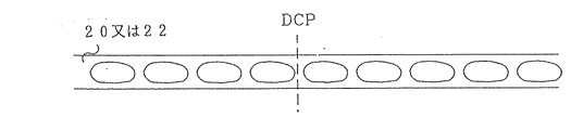
図3に示すように、光ディスクの信号トラック(20又は22)の左側から任意の地点(DCP)に至る区間(S1)に第1ユーザー情報が記録され、次の任意の期間が経過後、任意の地点(DCP、即ち、不連続記録位置)から右側方向に第2ユーザー情報が記録されたとすれば、信号トラック(20又は22)に記録された記録クロックの位相は図4Aのように不連続記録位置(DCP)で急激に変化するようになる。これは光ディスクの信号トラック(20又は22)に記録された記録クロックがソフトセクター方式の補助信号に含まれた基準クロック信号に基づいて発生されるためである。この記録クロックは光ディスク再生装置により図4Bのように不連続記録位置(DCP)から一定区間に当たる期間の間、大きいサイクルを有するか又は図4Cのように不連続記録位置(DCP)から一定区間に当たる期間の間、小さいサイクルを有するように再生される。このように信号トラック(20又は22)上の不連続記録位置(DCP)から一定区間に記録された記録クロック信号が大きいか又は小さいサイクルを有するように再生するのでその区間に記録されたユーザー情報が正確に再生されないようになる。
【0008】
このような、光ディスクの信号トラック上の不連続記録位置でのユーザー情報のエラーを防止するため、不連続記録位置に“可変周波数発振(Variable Frequency Oscilating、以下“VFO”と言う)信号”と言うクロック安定化情報を付加する方案が提案された。このクロック安定化情報は通常不連続記録位置から一つのセクター区間にわたって記録されるので光ディスクの信号トラックを不要に消耗する。これにより、クロック安定化情報の付加方法は光ディスクの信号トラック上の不連続記録位置の数が増加するにつれて光ディスクの記録容量を著しく少なくさせる短所を有している。
【0009】
【発明が解決しようとする課題】
従って、本発明の目的は、ユーザー情報が安定して再生されるようにすると共に光ディスクの記録容量が大きくなるように光ディスクの信号トラック上の不連続記録位置にユーザー情報を記録することのできる光ディスク記録方法及び装置を提供することにある。
【0010】
【課題を解決するための手段】
前記目的を達成するために、本発明による光ディスク記録方法は、信号トラックを単位ブロックに区分する補助信号が信号トラックとは別の領域にプリフォーマットされた光ディスクの信号トラックの不連続記録位置と隣接した単位ブロックの一部分にクロック安定化情報を記録する段階と、その単位ブロックの残りの部分にユーザー情報を記録する段階を含む。
【0011】
本発明による他の光ディスク記録方法は、信号トラックを単位ブロックに区分する補助同期信号と情報の伝送速度を指示する補助クロックとを含む補助信号が信号トラックとは異なる別の領域にプリフォーマットされた光ディスクから補助同期信号と補助クロックとを検出する第1段階と、補助同期信号と補助クロックを利用して信号トラック上の不連続記録位置と隣接した単位ブロックの一部分にクロック安定化情報を記録する第2段階と、補助同期信号と補助クロックを利用して不連続記録位置と隣接した単位ブロックの残りの部分にユーザー情報を記録する第3段階を含む。
【0012】
本発明によるさらに他の光ディスク記録方法は、信号トラックを単位ブロックに区分する補助同期信号と情報の伝送速度を指示する補助クロックとを含む補助信号が信号トラックとは異なる別の領域にプリフォーマットされた光ディスクから補助同期信号と補助クロックを検出する第1段階と、検出された補助クロックに基づいて基準クロックを発生する第2段階と、検出された補助同期信号と基準クロックを利用して信号トラック上の不連続記録位置と隣接した単位ブロックの一部分にクロック安定化情報を記録する第3段階と、クロック安定化情報と基準クロックを利用して不連続記録位置と隣接した単位ブロックの残りの部分にユーザー情報を記録する第4段階を含む。
【0013】
本発明によるさらに他の光ディスク記録方法は、信号トラックを単位ブロックに区分する補助同期信号と情報の伝送速度を指示する補助クロックを含む補助信号が信号トラックとは異なる別の領域にプリフォーマットされた光ディスクから補助クロックを検出する第1段階と、検出された補助クロックに基づいて基準クロックを発生する第2段階と、信号トラックに記録された同期信号を再生する第3段階と、再生された同期信号と基準クロックを利用して信号トラック上の不連続記録位置と隣接した単位ブロックの一部分にクロック安定化情報を記録する第4段階と、クロック安定化情報と基準クロックを利用して不連続記録位置と隣接した単位ブロックの残りの部分にユーザー情報を記録する第5段階を含む。
【0014】
本発明によるさらに他の光ディスク記録方法は、信号トラックを単位ブロックに区分する補助同期信号と情報の伝送速度を指示する補助クロックとを含む補助信号が信号トラックとは異なる別の領域にプリフォーマットされた光ディスクから補助同期信号と補助クロックを検出する第1段階と、検出された補助クロックに基づいて基準クロックを発生する第2段階と、信号トラックに記録された同期信号を再生する第3段階と、再生された同期信号、補助同期信号及び基準クロックを利用して信号トラック上の不連続記録位置と隣接した単位ブロックの一部分にクロック安定化情報を記録する第4段階と、クロック安定化情報と基準クロックを利用して不連続記録位置と隣接した単位ブロックの残りの部分にユーザー情報を記録する第5段階を含む。
【0015】
本発明によるさらに他の光ディスク記録方法は、信号トラックを単位ブロックに区分する補助同期信号と情報の伝送速度を指示する補助クロックとを含む補助信号が信号トラックとは異なる別の領域にプリフォーマットされた光ディスクから補助同期信号と補助クロックを検出する第1段階と、検出された補助クロックに基づいて基準クロックを発生する第2段階と、信号トラックに記録された同期信号を再生する第3段階と、再生された同期信号、補助同期信号及び基準クロックを利用して信号トラック上の不連続記録位置と隣接した単位ブロックの一部分にクロック安定化情報を記録する第4段階と、クロック安定化情報により擬似同期信号を発生する第5段階と、擬似同期信号と基準クロックを利用して不連続記録位置と隣接した単位ブロックの残りの部分にユーザー情報を記録する第5段階を含む。
【0016】
本発明によるさらに他の光ディスク記録方法は、信号トラックを単位ブロックに区分する補助同期信号と情報の伝送速度を指示する補助クロックとを含む補助信号が信号トラックとは異なる別の領域にプリフォーマットされた光ディスクから補助同期信号と補助クロックを検出する第1段階と、検出された補助クロックに基づいて基準クロックを発生する第2段階と、検出された補助同期信号に基づいて基準同期信号を発生する第3段階と、信号トラックに記録された同期信号を再生する第4段階と、再生された同期信号、補助同期信号及び基準クロックを利用して信号トラック上の不連続記録位置と隣接した単位ブロックの一部分にクロック安定化情報を記録する第5段階と、クロック安定化情報により擬似同期信号を発生する第6段階と、擬似同期信号と基準クロックを利用して不連続記録位置と隣接した単位ブロックの残りの部分にユーザー情報を記録する第7段階と、基準同期信号及び基準クロックを利用して不連続記録位置と隣接した単位ブロックに連結される少なくとも一つの後続単位ブロックにユーザー情報を記録する第8段階を含む。
【0017】
本発明による光ディスク記録装置は、信号トラックを単位ブロックに区分する補助信号が信号トラックとは別の領域にプリフォーマットされた光ディスクの信号トラック上の不連続記録位置と隣接した単位ブロックの一部分にクロック安定化情報を記録する第1記録手段と、その単位ブロックの残りの部分にユーザー情報を記録する第2記録手段とを備える。
【0018】
本発明による他の光ディスク記録装置は、信号トラックを単位ブロックに区分する補助同期信号と情報の伝送速度を指示する補助クロックとを含む補助信号が信号トラックとは異なる別の領域にプリフォーマットされた光ディスクから補助同期信号と補助クロックとを検出する補助信号検出手段と、補助信号検出手段からの補助同期信号及び補助クロックを利用して信号トラック上の不連続記録位置と隣接した単位ブロックの一部分にクロック安定化情報を記録する第1記録手段と、補助信号検出手段からの補助同期信号及び補助クロックを利用して不連続記録位置と隣接した単位ブロックの残りの部分にユーザー情報を記録する第2記録手段とを備える。
【0019】
本発明によるさらに他の光ディスク記録装置は、信号トラックを単位ブロックに区分する補助同期信号と情報の伝送速度を指示する補助クロックとを含む補助信号が信号トラックとは異なる別の領域にプリフォーマットされた光ディスクから補助同期信号と補助クロックを検出する補助信号検出手段と、補助信号検出手段からの補助クロックに基づいて基準クロックを発生する基準クロック発生手段と、補助信号検出手段からの補助同期信号と基準クロック発生手段からの基準クロックとを利用して信号トラック上の不連続記録位置と隣接した単位ブロックの一部分にクロック安定化情報を記録する第1記録手段と、第1記録手段からのクロック安定化情報と基準クロック発生手段からの基準クロックを利用して不連続記録位置と隣接した単位ブロックの残りの部分にユーザー情報を記録する第2記録手段を備える。
【0020】
本発明によるさらに他の光ディスク記録装置は、信号トラックを単位ブロックに区分する補助同期信号と情報の伝送速度を指示する補助クロックとを含む補助信号が信号トラックとは異なる別の領域にプリフォーマットされた光ディスクから補助クロックを検出する補助信号検出手段と、補助信号検出手段からの補助クロックに基づいて基準クロックを発生する基準クロック発生手段と、信号トラックに記録された同期信号を再生する再生手段と、再生手段からの再生された同期信号と基準クロック発生手段からの基準クロックを利用して信号トラック上の不連続記録位置と隣接した単位ブロックの一部分にクロック安定化情報を記録する第1記録手段と、第1記録手段からのクロック安定化情報と基準クロック発生手段からの基準クロックを利用して不連続記録位置と隣接した単位ブロックの残りの部分にユーザー情報を記録する第2記録手段を備える。
【0021】
本発明によるさらに他の光ディスク記録装置は、信号トラックを単位ブロックに区分する補助同期信号と情報の伝送速度を指示する補助クロックとを含む補助信号が信号トラックとは異なる別の領域にプリフォーマットされた光ディスクから補助同期信号と補助クロックを検出する補助信号検出手段と、補助信号検出手段からの補助クロックに基づいて基準クロックを発生する基準クロック発生手段と、信号トラックに記録された同期信号を再生する再生手段と、再生手段からの再生された同期信号、補助信号検出手段からの補助信号及び基準クロック発生手段からの基準クロックを利用して信号トラック上の不連続記録位置と隣接した単位ブロックの一部分にクロック安定化情報を記録する第1記録手段と、第1記録手段からのクロック安定化情報と基準クロック発生手段からの基準クロックを利用して不連続記録位置と隣接した単位ブロックの残りの部分にユーザー情報を記録する第2記録手段を備える。
【0022】
本発明によるさらに他の光ディスク記録装置は、信号トラックを単位ブロックに区分する補助同期信号と情報の伝送速度を指示する補助クロックとを含む補助信号が信号トラックとは異なる別の領域にプリフォーマットされた光ディスクから補助同期信号と補助クロックを検出する補助信号検出手段と、補助信号検出手段からの補助クロックに基づいて基準クロックを発生する基準クロック発生手段と、信号トラックに記録された同期信号を再生する再生手段と、補助信号検出手段からの補助同期信号、再生手段からの再生された同期信号及び基準クロック発生手段からの基準クロックを利用して信号トラック上の不連続記録位置と隣接した単位ブロックの一部分にクロック安定化情報を記録する第1記録手段と、第1記録手段からのクロック安定化情報により擬似同期信号を発生する擬似同期発生手段と、擬似同期発生手段からの擬似同期信号と基準クロック発生手段からの基準クロックを利用して不連続記録位置と隣接した単位ブロックの残りの部分にユーザー情報を記録する第2記録手段を備える。
【0023】
本発明による光ディスク記録装置は、信号トラックを単位ブロックに区分する補助同期信号と情報の伝送速度を指示する補助クロックとを含む補助信号が信号トラックとは異なる別の領域にプリフォーマットされた光ディスクから補助同期信号と補助クロックを検出する補助信号検出手段と、補助信号検出手段からの前記補助クロックに基づいて基準クロックを発生する基準クロック発生手段と、補助信号検出手段からの補助クロックに基づいて基準同期信号を発生する基準同期発生手段と、信号トラックに記録された同期信号を再生する再生手段と、補助信号検出手段からの補助同期信号、再生手段からの再生された同期信号及び基準クロック発生手段からの基準クロックを利用して信号トラック上の不連続記録位置と隣接した単位ブロックの一部分にクロック安定化情報を記録する第1記録手段と、第1記録手段からのクロック安定化情報により擬似同期信号を発生する擬似同期発生手段と、擬似同期発生手段からの擬似同期信号と基準クロック発生手段からの基準クロックを利用して不連続記録位置と隣接した単位ブロックの残りの部分にユーザー情報を記録する第2記録手段と、基準同期発生手段からの基準同期信号及び基準クロック発生手段からの基準クロックを利用して不連続記録位置と隣接した単位ブロックに連結される少なくとも一つの後続単位ブロックにユーザー情報を記録する第3記録手段を備える。
【0024】
【作用】
前記の構成により、本発明では信号トラックとは異なる別の領域に補助信号がプリフォーマットされた光ディスクの信号トラック上の不連続記録位置と隣接したブロック区間にクロック安定化情報がユーザー情報と共に記録される。これにより、信号トラック上の不連続記録位置と隣接したブロック区間に記録されたユーザー情報は安定して再生されることは勿論、光ディスクの記録容量が大きくなる。そして、本発明では再生同期信号と補助信号に含まれた補助同期信号との位相の先後関係により光ディスクの信号トラック上の不連続記録位置とクロック安定化情報の間に余白区間は選択的に生成されるようにする。この結果、クロック安定化情報は再生同期信号に同期されるように不連続記録位置と隣接したブロック区間に記録するようになる。又、本発明は基準クロックが補助信号に含まれた補助クロックに同期された場合にのみ光ディスクに情報を記録することにより光ディスクの記録容量が一定して維持するようにすると共にエラーの発生を最小化する。
【0025】
【発明の実施の形態】
以下、本発明の望ましい実施形態を添付した図5〜図17を参照して詳細に説明する。
図5は、本発明の実施形態による光ディスク記録装置を図示する。図5において、光ディスク記録装置は光ディスク(24)を回転させるスピンドルモーター(26)と、光ピックアップ(28)に接続されたサーボ部(30)と、スピンドルモーター(26)に接続されたモーター駆動部(32)を備ていえる。光ピックアップ(28)は、図2に示したような光ディスク(24)の溝のトラック(22)に一つのメイン光ビーム(MB)と二つの補助光ビーム(SB1、SB2)を照射してメイン光ビーム(MB)で情報を記録し、補助光ビーム(SB1、SB2)でプリフォーマットされた補助信号を読み取る。光ピックアップ(28)は、レーザーダイオード(LD)及び光検出器(PD)の間に位置してレーザー光ビームを分割するビームスプリッター(BS)と、光ディスク(24)及びビームスプリッター(BS)の間に設置された対物レンズ(OL)を備える。対物レンズ(OL)はビームスプリッター(BS)から光ディスク(24)の方に進むレーザー光ビームを集光する。ビームスプリッター(BS)はレーザーダイオード(LD)からのレーザー光ビームが対物レンズ(OL)を経由して光ディスク(24)の表面に照射されるようにすると共に、光ディスク(24)により反射された反射光ビームがセンサーレンズ(SL)を経由して光検出器(PD)の方に進むようにする。センサーレンズ(SL)はビームスプリッター(BS)から光検出器(PD)の方に進むる光ビームを集束して非点数差法により焦点を調節する。レーザーダイオード(LD)で発生した光ビームは回折格子(GT)により三つの光ビーム(MB,SB1、SB2)で分離される。そして、回折格子(GT)により分離された光ビーム(MB,SB1、SB2)はビームスプリッター(BS)を経由し、対物レンズ(OL)で図2で示すように光ディスク(24)の溝のトラック(22)の上に集光される。光ディスク(24)の溝のトラック(22)により反射される光ビーム(MB,SB1、SB2)は対物レンズ(OL)及びビームスプリッター(BS)を経由してセンサーレンズ(SL)によって光検出器(PD)の表面に集光する。光検出器(PD)は補助光ビーム(SB1、SB2)を電気的信号に変換する。サーボ部(30)は光検出器(PD)からの電気的信号により光ピックアップ(28)内のアクチュエータ(ACT)を駆動してフォーカシングサーボ、トラッキングサーボ等を行う。一方、モーター駆動部(32)はサーボ部(30)からの信号によりスピンドルモーター(26)の回転速度を調節する。
【0026】
光ディスク記録装置は、さらに光ピックアップ(28)の光検出器(PD)に直列接続した搬送波信号検出器(34)と補助信号デコーダ(36)を備える。搬送波信号検出器(34)は光検出器(PD)からの電気的信号から搬送波信号(Pc)を検出して、補助信号デコーダ(36)は搬送波信号(Pc)から補助アドレス(PAdd)及び補助クロック(PCLK)と図6に示したような補助同期信号(PYre)をデコードする。この補助同期信号(PYre)は光ディスク(24)の信号トラック(20又は22)を一定の大きさの単位ブロックに区分し、補助アドレス(PAdd)は単位ブロックの各々の物理的位置を指示する。又、本発明の実施形態による光ディスク記録装置は、補助信号デコーダ(36)から補助同期信号(PYre)を入力する基準同期信号発生器(38)と、基準クロック発生器(40)から安定化情報制御信号(CVFO)を入力する擬似同期信号発生器(42)と、基準クロック発生器(40)から基準クロック(SCLK)を利用してVFO信号を発生するVFO信号発生器(44)を備える。基準同期信号発生器(38)は補助同期信号(PYre)に位相同期された基準同期信号(SYre)を発生する。基準クロック発生器(40)は補助信号デコーダ(36)からの補助クロック(PCLK)に位相及び周波数が同期された図6に示したような基準クロック(SCLK)を発生する。この基準クロック(SCLK)の周波数は記録開始から、一定期間の間、補助クロック(PCLK)のN倍から補助クロックのM倍へ高くなる。この一定期間が経過した後、基準クロック(SCLK)の周波数は再び補助クロック(PCLK)のM倍から補助クロック(PCLK)のN倍へ低くなるようになる。これを詳細に説明すると、基準クロック(SCLK)は不連続記録位置(DCP)からVFO信号の記録が完了される光ディスク(24)の信号トラック(20又は22)上の位置に至る区間に該当する期間の間に補助クロック(PCLK)のM倍から補助クロック(PCLK)のN倍まで変化する周波数を持つようになる。このVFO信号が記録された後に基準クロック(SCLK)はVFO信号が記録された区間の終了位置から不連続記録位置(DCP)と隣接した単位ブロックの終了地点に至る区間に該当する期間又は一定の数の単位ブロックに該当する期間の間に補助クロック(PCLK)のM倍からN倍まで漸進的に低くなる周波数を持つようになる。そして基準クロック発生器(40)は制御部(50)からの図6に示したような記録スタート信号(WRsta)と補助信号デコーダ(36)からの補助同期信号(PYre)を利用して安定化情報制御信号(CVFO)を発生する。この安定化情報制御信号(CVFO)は、光ディスク(24)の信号トラック(20又は22)に記録されたクロック信号の位相が急激に変化する光ディスク(24)の信号トラック(20又は22)上の不連続記録位置(DCP)にVFO信号を挿入できるようにする。又、安定化情報制御信号(CVFO)はVFO信号が不連続記録位置(DCP)と隣接した単位ブロックの一部の区間に記録されるように図6に示すように光ディスク(24)の信号トラック(20又は22)上の単位ブロックに比べてかなり短い幅のパルスを持つ。又、基準クロック発生器(40)は基準クロック(SCLK)が補助クロック(PCLK)に比べて一定の範囲の倍数、即ちN倍からM倍に至る範囲の周波数を持つ場合に特定論理(例えば、ハイ論理)を有するロッキング信号(LK)を発生することができる。擬似同期信号発生器(42)は、安定化情報制御信号(CVFO)の終了時点(例えば、下降エッジ)から一定の期間の間、特定論理(例えば、ハイ論理)を維持する擬似同期信号(PSre)を発生する。この擬似同期信号(PSre)は基準同期信号に比べて幅が狭い特定論理のパルスを持つ。このために擬似同期信号発生器(42)は単安定マルチバイブレータを具備することができる。
【0027】
さらに、光ディスク記録装置は、ユーザー情報を入力する記録情報処理部(46)を有し、かつVFO信号発生器(44)からのVFO信号と記録情報処理部(46)からの記録信号とを選択的に光制御器(48)に供給する制御用スイッチ(SW1)を備える。記録情報処理部(46)はユーザー情報を一定の大きさで分割してユーザーブロック情報を生成すると共に、このユーザーブロック情報の先頭に補助信号デコーダ(36)からの補助アドレス(PAdd)と擬似同期信号発生器(42)からの擬似同期信号(PSre)又は基準同期信号発生器(38)からの基準同期信号(SYre)を追加してユーザー情報ブロックを形成させる。又、記録情報処理部(46)はユーザー情報を記録信号として基準クロック発生器(40)からの基準クロック(SCLK)に合わせて制御用スイッチ(SW1)に供給する。擬似同期信号(PSre)が含まれたユーザー情報ブロックは補助クロック(PCLK)のM倍の周波数を持つ基準クロック(SCLK)により伝送されることによりVFO信号と共に光ディスク(24)の信号トラック(20又は22)上の一つの単位ブロックに記録される。即ち、擬似同期信号(PSre)が含まれたユーザー情報ブロックは、時間的に圧縮されることにより基準同期信号(SYre)が含まれたユーザー情報ブロックより短いサイクルを持つようになる。制御用スイッチ(SW1)は基準クロック発生器(40)からの安定化情報制御信号(CVFO)の論理状態によりVFO信号と記録信号を選択的に光制御器(48)の方に伝送する。これを詳細に説明すると、制御用スイッチ(SW1)は、安定化情報制御信号(CVFO)が特定論理(即ち、ハイ論理)を維持する場合には、VFO信号発生器(44)からのVFO信号を光制御器(48)に供給する。これに対して、安定化情報制御信号(CVFO)が基底論理(例えば、ロー論理)を維持する場合には記録情報処理部(46)からの記録信号を光制御器(48)の方に伝送する。光制御器(48)は制御用スイッチ(SW1)の出力信号の論理値によりレーザーダイオード(LD)を断続してユーザー情報ブロックが光ディスク(24)の信号トラック、即ち山のトラック(20)又は溝のトラック(22)に記録されるようにする。この時、信号トラック(20又は22)の不連続記録位置(DCP)と隣接した単位ブロック、即ち記録開始の時、ユーザー情報の最前部分が記録される信号トラック(20又は22)上の任意の単位ブロックには図6でのようにクロック安定化情報であるVFO信号を始めとして擬似同期信号(PSre)ブロック識別コードとユーザーブロック情報が順次に記録される。反面に不連続記録位置(DCP)と離れたブロック区間、各々には基準同期信号(SYre)ブロック識別コード及びユーザーブロック情報が記録される。
【0028】
終わりに、制御部(50)はサーボ部(30)とモーター駆動部(32)の動作の如何を制御すると共に、光制御器(48)の動作モードを制御する。又、制御部(50)は記録開始の時に特定論理(例えば、ハイ論理)のパルスを持つ記録開始信号(WRsta)を発生する。この記録開始信号(WRsta)は基準クロック発生器(40)に供給されて光ディスク(24)上の信号トラック(20又は22)上の記録不連続地点から一定の区間にクロック安定化情報であるVFO信号が記録され得るようにする。又、制御部(50)は基準クロック発生器(40)からロッキング信号(LK)を入力できる。このロッキング信号(LK)の論理状態により制御部(50)は光制御器(48)の記録動作を選択的にイネーブルさせる。制御部(50)はロッキング信号(LK)が特定論理(例えば、ハイ論理)を維持する場合にだけ光制御器(48)が記録動作を実行するようにして光ディスク(24)の記録密度が一定して維持されるようにすると共にエラーの発生を防止する。
【0029】
図7は図5に示した基準クロック発生器(40)を詳細に示すブロックである。図7において、基準クロック発生器(40)は電圧制御発振器(52)からの基準クロック(SCLK)を第1ANDゲート(62)を経由して入力する分周器(54)と、この分周器(54)の出力信号を入力する位相比較器(56)と周波数比較器(58)を備える。第1ANDゲート(62)は安定化情報制御信号(CVFO)により電圧制御発振器(52)から分周器(54)に供給される基準クロック(SCLK)を切り換える。第1ANDゲート(62)は安定化情報制御信号(CVFO)がハイ論理を維持する場合に電圧制御発振器(52)からの基準クロック(SCLK)が分周器(54)に供給されないようにする。即ち、第1ANDゲート(62)はロー論理のロー信号を分周器(54)に供給する。これにより、分周器(54)でもロー論理又はハイ論理の論理信号が発生する。この時、位相比較器(56)は、図5に示された補助信号デコーダ(36)からの補助クロック(PCLK)と分周器(54)からの論理信号を位相比較するので急激に増加する電圧信号を持つ位相エラー信号を積分器(60)に供給する。分周器(54)からの論理信号と補助クロック(PCLK)を周波数比較する周波数比較器(58)も急激に増加する電圧信号を持つ周波数エラー信号を積分器(60)に供給する。積分器(60)は位相比較器(56)からの位相エラー信号と周波数比較器(58)からの周波数エラー信号を各々積分して、これら信号に含まれた高周波成分の雑音信号を除去する。積分器(60)からの積分された位相エラー信号及び周波数エラー信号により電圧制御発振器(52)は基準クロック(SCLK)の周波数を補助クロック(PCLK)のN倍から補助クロック(PCLK)のM倍まで急激に高める。この結果、基準クロック(SCLK)の周波数はクロック安定化情報制御信号(CVFO)の上昇エッジで補助クロック(PCLK)のN倍からM倍に急激に高まった後、クロック安定化情報制御信号(CVFO)の下降エッジ指示まで補助クロック(PCLK)のM倍を維持するようになる。反面に安定化情報制御信号(CVFO)がロー論理を維持する場合、第1ANDゲート(62)は電圧制御発振器(52)からの基準クロック(SCLK)が分周器(54)に供給されるようにする。この場合、分周器(54)は第1ANDゲート(62)からの基準クロック(SCLK)をN分周する。この時、位相比較器(56)は補助クロック(PCLK)と分周器(54)からの分周されたクロック信号との位相差により漸進的に減少される電圧信号を持つ位相エラー信号を発生する。同じように、周波数比較器(58)も分周器(54)からのクロック信号と補助クロック(PCLK)との周波数の差異により電圧が漸進的に減少する周波数エラー信号を発生する。すると、積分器(60)を経由して位相エラー信号と周波数エラー信号を入力する電圧制御発振器(52)は基準クロック(SCLK)の周波数を補助クロック(PCLK)のM倍から補助クロック(PCLK)のN倍まで漸進的に低くするようになる。これにより、基準クロック(SCLK)の周波数はクロック安定化情報制御信号(CVFO)の下降エッジから一定の期間の間(例えば、クロック安定化情報(CVFO)が記録された信号トラック(20、22)上の区間の終了位置からそのクロック安定化情報が記録された単位ブロックの終了位置までの区間に当たる期間)に補助クロック(PCLK)のM倍からN倍まで漸進的に低くなる。併せて、この基準クロック(SCLK)は図5に示したVFO信号発生器(44)及び記録情報処理部(46)に供給される。又、分周された基準クロック信号が補助クロック(PCLK)に比べて一定の範囲の周波数の差異を有する場合、即ち、基準クロック(SCLK)が補助クロック(PCLK)よりN倍ないしM倍の周波数を有する場合に、周波数比較器(58)は特定論理(例えば、ハイ論理)を有するロッキング信号(LK)を発生する。このロッキング信号(LK)は図5に示した制御部(50)に供給される。
【0030】
そして、基準クロック発生器(40)は、図5に示した制御部(50)から記録スタート信号(WRsta)を入力する第1ラッチ(64)と、図5に示した補助信号デコーダ(36)から補助同期信号(PYre)を入力するNANDゲート(66)を更に備える。第1ラッチ(64)は自身のセット端子(S)に特定論理(即ち、ハイ論理)の記録スタート信号(WRsta)が入力される場合に自身の出力端子(Q)にハイ論理の出力信号を発生する。NANDゲート(66)は第1ラッチ(64)の出力信号と補助同期信号(PYre)をNAND演算し、その結果により第2ラッチ(68)を選択的にトグルさせる。すなわち、NANDゲート(66)は第1ラッチ(64)の出力信号と補助同期信号(PYre)が共にハイ論理を維持する場合にのみロー論理のパルスを発生させる。第2ラッチ(68)はNANDゲート(66)からのロー論理のパルスの上昇エッジから自身の出力端子(Q)上の論理信号をロー論理からハイ論理に変化させる。第1及び第2ラッチ(64,68)は自身のリセット端子(R)で印加する基底論理(即ち、ロー論理)の安定化情報制御信号(CVFO)により初期化される。
【0031】
又、基準クロック発生器(40)は電圧制御発振器(52)からの基準クロック(SCLK)を入力する第2ANDゲート(70)と、第2ラッチ(68)の出力信号を入力するカウンター(72)と、このカウンター(72)からキャリ信号を入力するインバーター(74)を備える。第2ANDゲート(70)は安定化情報制御信号(CVFO)が特定論理(即ち、ハイ論理)を維持する間にだけ電圧制御発振器(52)からの基準クロック(SCLK)をカウンター(72)のクロック端子(CLK)の方に伝送する。カウンター(72)は第2ラッチ(68)から自身のリセット端子(R)の方にハイ論理の論理信号が印加する間に第2ANDゲート(70)から供給する基準クロック(SCLK)により加算カウントする。そして、カウンター(72)はカウント値が“K”に到達するときに、ハイ論理のキャリ信号を発生する。又、カウンター(72)はキャリ信号を発生した後、第2ラッチ(68)から自身のリセット端子(R)の方に供給するロー論理の論理信号によりカウント動作を中止するようになる。インバーター(74)はカウンター(72)からのキャリ信号を反転し、その反転されたキャリ信号を安定化情報制御信号(CVFO)として第1及び第2ANDゲート(62,70)、第1及び第2ラッチ(64,68)、図5に示した制御用スイッチ(SW1)及び擬似同期信号発生器(42)に供給する。結果的に、第2ラッチ(68)、第2ANDゲート(70)、カウンター(72)及びインバーター(74)は記録開始の時、一番目の補助同期信号(PYre)の下降エッジから一定の幅のハイ論理パルスを有する安定化情報制御信号(CVFO)を発生する単安定パルス発生器の機能を行う。
【0032】
図8は、本発明の他の実施形態による光ディスク記録装置のブロックを図示する。図8に示した他の実施形態による光ディスク記録装置は図5に示した光ディスク記録装置に比べて制御用スイッチ(SW1)と光制御器(48)の間に接続された第2制御用スイッチ(SW2)を更に備える。併せて、他の実施形態による光ディスク記録装置は図5に示した基準クロック発生器(40)の代わりに適応型基準クロック発生器(76)を備える。
【0033】
この適応型基準クロック発生器(76)は図5に示した基準クロック発生器(40)と同じく図9に示したような基準クロック(SCKL)を発生し、その基準クロック(SCKL)を記録情報処理部(46)及びVFO信号発生器(44)に供給する。そして、適応型基準クロック発生器(76)図9でのように記録スタート信号(WRsta)は発生した後、一番目の補助同期信号(PYre)の下降エッジから順次に配列される余白制御信号(Cspc)と安定化情報制御信号(CVFO)を発生する。この余白制御信号(Cspc)により第2制御用スイッチ(SW2)は記録情報処理部(46)を光制御器(48)に選択的に連結させることによって光ディスク(24)の信号トラック(20又は22)に情報が記録されない余白区間か生成されるようにする。この余白区間は、光ディスク(24)の信号トラック(20又は22)上の不連続記録位置(DCP)とクロック安定化情報区間の間に位置する。即ち、光ディスク(24)の信号トラック(20又は22)上の不連続記録位置(DCP)と隣接したブロック区間には図9でのように余白区間(SPC)、VFO信号(VFO)、擬似同期信号(PSre)、ブロック識別信号及びユーザーブロック情報が記録される。
【0034】
又、本発明の他の実施形態による光ディスク記録装置は、光ピックアップ(28)内の光検出器(PD)の出力信号を再生して再生同期信号(RYre)を適応型基準クロック発生器(76)に供給する再生信号処理部(51)を更に備えることができる。この場合、適応型基準クロック発生器(76)は再生同期信号(RYre)と補助同期信号(PYre)の位相の先後関係により余白制御信号(Cspc)の論理状態を変化させる。適応型基準クロック発生器(76)は、図10及び図11のように再生同期信号(SYre)の位相が補助同期信号(PYre)よりはやい場合には余白制御信号(Cspc)が基底論理(即ち、ロー論理)を維持するようにして光ディスク(24)の信号トラック(20又は22)上に余白区間が現れないようにする。即ち、光ディスク(24)の信号トラック(20又は22)上の不連続記録位置(DCP)と隣接した単位ブロックにはVFO信号(VFO)、擬似同期信号(PSre)、ブロック識別信号及びユーザーブロック情報が記録される。一方、図12のように、再生同期信号(RYre)の位相が補助同期信号(PYre)より遅い場合、適応型基準クロック発生器(76)は余白制御信号(Cspc)が補助同期信号(PYre)の下降エッジから再生同期信号(RYre)の上昇エッジまでハイ論理とし、光ディスク(24)の信号トラック(20又は22)上に余白区間を生成させる。即ち、光ディスク(24)の信号トラック(20又は22)上の不連続記録位置(DCP)と隣接した単位ブロックには図9のように余白区間(SPC)、VFO信号(VFO)、擬似同期信号(PSre)、ブロック識別信号及びユーザーブロック情報が記録される。
【0035】
図13は図8に示した適応型基準クロック発生器(76)の第1実施形態を詳細に示す回路図である。図13において、適応型基準クロック発生器(76)は図7に示した基準クロック発生器(40)と比較するとき、NANADゲート(66)と第2ラッチ(68)の間に直列接続した第3ラッチ(78)、第2カウンター(84)及び第2インバーター(86)と、電圧制御発振器(52)と第2カウンター(84)のクロック端子(CLK)間に直列接続した第2分周器(80)及び第3ANDゲート(82)を更に備える。また、適応型基準クロック発生器(76)は図7に示した第1ANDゲート(62)の代わりに電圧制御発振器(52)からの基準クロック(SCLK)、第1インバーター(74)からの安定化情報制御信号(CVFO)及び第2インバーター(86)からの余白制御信号(Cspc)を入力する第4ANDゲート(88)を備える。
【0036】
第3ラッチ(78)はNANDゲート(66)の出力信号の上昇エッジで自身の出力端子(Q)上の論理信号をロー論理からハイ論理に変化させる。即ち、第3ラッチ(78)は図9のように記録開始信号(WRsta)が発生した後、一番目に入力する補助同期信号(PYre)の下降エッジ指示にハイ論理の出力信号を発生するようになる。第2分周器(80)は電圧制御発振器(52)からの基準クロック(SCLK)をN分周し、その分周された基準クロックを第3ANDゲート(82)に供給する。第3ANDゲート(82)は図9に示したような余白制御信号(Cspc)が特定論理(即ち、ハイ論理)を維持する間にのみ第2分周器(80)からの分周された基準クロックを第2カウンター(84)のクロック端子(CLK)の方に伝送する。第2カウンター(84)は第3ラッチ(78)から自身のリセット端子(R)の方にハイ論理の論理信号が印加する間に第3ANDゲート(82)からの分周された基準クロックにより加算カウントする。又、第2カウンター(84)はカウント値が“L”に到達するときにハイ論理のキャリ信号を発生する。又、第2カウンター(84)はキャリ信号を発生した後、第3ラッチ(78)から自身のリセット端子(R)の方に供給されるロー論理の論理信号によりカウント動作を中止するようになる。第2インバーター(86)は第2カウンター(84)からのキャリ信号を反転し、その反転させたキャリ信号を余白制御信号(Cspc)として第3及び第4ANDゲート(82,88)、第3ラッチ(78)と図7に示したように第2制御用スイッチ(SW2)に供給する。結果的に、第3ラッチ(78)、第3ANDゲート(82)、第2カウンター(84)及び第2インバーター(86)は記録開始の時、一番目の補助同期信号(PYre)の下降エッジから一定の幅のハイ論理パルスを有する余白制御信号(Cspc)を発生する単安定パルス発生器の機能を行う。この余白制御信号(Cspc)により第2ラッチ(68)は安定化情報制御信号(CVFO)の発生時点を決定する。即ち、第2ラッチ(68)は第2インバーター(86)からの余白制御信号(Cspc)の下降エッジから第1カウンター(72)のカウント動作を開始させた後、第1インバーター(74)からのロー論理の安定化情報制御信号(CVFO)により初期化することにより図9のように安定化情報制御信号(CVFO)が余白制御信号(Cspc)の下降エッジから一定の幅のハイ論理を有するようにする。
【0037】
一方、第4ANDゲート(88)は余白制御信号(Cspc)及び安定化情報制御信号(CVFO)により電圧制御発振器(52)から第1分周器(54)に供給される基準クロック(SCLK)を切り換える。第4ANDゲート(88)は余白制御信号(Cspc)及び安定化情報制御信号(CVFO)のうち、いずれの一つでもハイ論理を維持する場合に電圧制御発振器(52)からの基準クロック(SCLK)が第1分周器(54)に供給されないようにする。即ち、第4ANDゲート(88)は光ディスク(24)の信号トラック(20又は22)上に余白信号とVFO信号が記録する期間には、基準クロック(SCLK)が第1分周器(54)に供給されないようにする。これとは異なり、余白制御信号(Cspc)と安定化情報制御信号(CVFO)がロー論理を維持する場合に、第4ANDゲート(88)は電圧制御発振器(52)からの基準クロック(SCLK)が第1分周器(54)に供給されるようにする。
【0038】
前記第2及び第3ラッチ(68,78)、第3及び第4ANDゲート(82,88)、分周器(80)、第2カウンター(86)及び第2インバーター(86)を以外の適応型基準クロック発生器(76)の残りの構成要素に対する作動説明は図7と同じであるので省略する。
【0039】
図14は、図8に示した適応型基準クロック発生器(76)の第2実施形態を詳細に示す回路図である。図14に示した適応型基準クロック発生器(76)は第4ANDゲート(88)がクロック調節器(90)で置き換えた以外は、図13に示した適応型基準クロック発生器(76)と同じ回路構成を持つ。このクロック(90)は余白制御信号(Cspc)がイネーブルされる時点から一定の期間の間(例えば、不連続記録地点から一つの単位ブロックが終了される地点までの区間に当たる期間の間)基準クロック(SCLK)の周波数が補助クロック(PCLK)のM倍を一定して維持するようにする。このためにクロック調節器(90)は第2インバーター(86)からの余白制御信号(Cspc)がロー論理からハイ論理に変化された後、一つの単位ブロックに当たる期間の間、一定のサイクル毎に電圧制御発振器(52)から第1分周器(54)の方に伝送する基準クロック(SCLK)を一つずつ除去する。この場合、位相比較器(56)から発生される位相エラー信号と周波数(58)から発生される周波数エラーが一定のサイクル毎に一度ずつ増加してから減少する。すると、位相エラー信号及び周波数エラー信号に応答する電圧制御発振器(52)は基準クロック(SCLK)の位相及び周波数を調節することにより基準クロック(SCLK)の位相が補助クロック(PCLK)の位相と一致するようにすると共に、基準クロック(SCLK)の周波数が補助クロック(PCLK)に比べてM倍に一定して維持するようにする。反対に、余白制御信号(Cspc)及び安定化情報制御信号(CVFO)が基底論理(ロー論理)を維持する場合、クロック調節器(90)は電圧制御発振器(52)からの基準クロック(SCLK)をそのまま第1分周器(54)に伝達することによって基準クロック(SCLK)の周波数を補助クロック(PCLK)のN倍に一定に維持する。
【0040】
図15は図14に示したクロック調節器(90)を詳細に図示する回路図である。図15において、クロック調節器(90)は図14に示した第1及び第2インバーター(74、86)からの安定化情報制御信号(CVFO)と余白制御信号(Cspc)を入力するORゲート(92)と、図14に示した電圧制御発振器(52)からの基準クロック(SCLK)を共通的に入力する第5ANDゲート(94)、第3分周器(96)及びエクスクルーシブOR(以下、“XOR”と言う)ゲート(98)を備える。ORゲート(92)は安定化情報制御信号(CVFO)と余白制御信号(Cspc)をOR演算し、この二つ信号のハイ論理期間の間、ハイ論理を維持するパルス信号を発生する。第5ANDゲート(94)はORゲート(92)の出力信号がハイ論理を維持する期間に基準クロック(SCLK)を第3カウンター(100)のクロック端子(CLK)に伝送する。第3カウンター(100)は第5ANDゲート(94)からの自身のクロック端子(CLK)に供給するクロック信号の数をカウントする。一方、第3分周器(96)は基準クロック(SCLK)を一定の分周比(例えば4)で分周し、その分周された基準クロックを第6ANDゲート(102)を経由して第4カウンター(104)に供給する。第4カウンター(104)は第6ANDゲート(102)からの分周された基準クロック数をカウントする。第3カウンター(100)のカウント値と第4カウンター(104)のカウント値は比較器(106)により比較される。この比較器(106)は、この二つのカウント値が同じ場合にハイ論理の比較信号を第6ANDゲート(102)に供給すので、第3分周器(96)から分周された基準クロックが第4カウンター(104)及びXORゲート(98)に供給されないようにする。即ち、第6ANDゲート(102)は、記録開始の時から第4カウンター(104)のカウント値が第3カウンター(100)のカウント値と同じくなるときまで、分周された基準クロックをXORゲート(98)に供給するようになる。XORゲート(98)は第6ANDゲート(102)からの分周された基準クロックがハイ論理を維持するとき毎に基準クロック(SCLK)の位相を180°反転させることにより、図14に示した第1分周器(54)に供給される基準クロック(SCLK)から1サイクルの基準クロックを消滅させる。第3分周器(96)の分周比は余白制御信号(Cspc)のハイ論理の幅と安定化情報制御信号(CVFO)のハイ論理の幅の合に該当する期間と単位ブロックの期間との比により決定される。
【0041】
図16は図8に示した適応型基準クロック発生器(76)の第3実施形態を詳細に示す回路図である。この適応型基準クロック発生器(76)は電圧制御発振器(52)からの基準クロック(SCLK)を第1ANDゲート(108)を経由して入力する第1分周器(54)と、第1分周器(54)の出力信号を入力する位相比較器(56)と周波数比較器(58)を備える。第1ANDゲート(108)は切換制御信号により基準クロック(SCLK)を切り換える。この第1ANDゲート(108)は切換制御信号がハイ論理を維持する場合に、電圧制御発振器(52)からの基準クロック(SCLK)が第1分周器(54)に供給されないようにする。即ち、第1ANDゲート(108)はロー論理の論理信号を第1分周器(54)に供給する。これにより、第1分周器(54)でもロー論理又はハイ論理の論理信号が発生される。この時、位相比較器(56)は図8に示した補助信号デコーダ(36)からの補助クロック(PCLK)と第1分周器(54)からの論理信号を位相比較するので急激に増加する電圧信号を持つ位相エラー信号を積分器(60)に供給する。第1分周器(54)からの論理信号を補助クロック(PCLK)を周波数比較する周波数比較器(58)も急激に増加する電圧信号を持つ周波数エラー信号を積分器(60)に供給する。積分器(60)は位相比較器(56)からの位相エラー信号と周波数比較器(58)からの周波数エラー信号を各々積分し、これらの信号に含まれた高周波成分の雑音信号を除去する。積分器(60)からの積分された位相エラー信号及び周波数エラー信号により電圧制御発振器(52)は基準クロック(SCLK)の周波数を補助クロック(PCLK)のN倍から補助クロック(PCLK)のM倍まで急激に高める。この結果、基準クロック(SCLK)の周波数は切換制御信号の上昇エッジで補助クロック(PCLK)のN倍からM倍に急激に高まった後、切換制御信号の下降エッジまで補助クロック(PCLK)のM倍を維持するようになる。切換制御信号がロー論理を維持する場合、第1ANDゲート(108)は電圧制御発振器(52)からの基準クロック(SCLK)を第1分周器(54)に供給する。この場合、第1分周器(54)は第1ANDゲート(108)からの基準クロック(SCLK)をN分周する。この時、位相比較器(56)は補助クロック(PCLK)と第1分周器(54)からの分周されたクロック信号との位相差により漸進的に減少する電圧信号を持つ位相エラー信号を発生する。同様に、周波数比較器(58)も第1分周器(54)からのクロック信号と補助クロック(PCLK)との周波数差により電圧が漸進的に減少する周波数エラー信号を発生する。すると、積分器(60)を経由して位相エラー信号と周波数エラー信号を入力する電圧制御発振器(52)は基準クロック(SCLK)の周波数を補助クロック(PCLK)のM倍から補助クロック(PCLK)のN倍まで漸進的に低くする。これにより、基準クロック(SCLK)の周波数は切換制御信号の下降エッジ(即ち、クロック安定化情報の記録が終了する信号トラック(20又は22)上の位置)から一定の期間の間(例えば、クロック安定化情報が記録された単位ブロックの終了位置までの区間に当たる期間)に補助クロック(PCLK)のM倍からN倍に漸進的に低くなる。この記録クロック(SCLK)は図8に示したVFO信号発生器(44)及び記録情報処理部(46)に供給される。又、周波数比較器(58)は分周された基準クロックが補助クロック(PCLK)に比べて一定の範囲の周波数差を有する場合、即ち基準クロック(SCLK)が補助クロック(PCLK)よりN倍ないしM倍の周波数を有する場合に特定論理(例えば、ハイ論理)を有するロッキング信号(LK)を発生する。このロッキング信号(LK)は図8に示した制御部(50)に供給される。
【0042】
そして、適応型基準クロック発生器(76)は図8に示した制御部(50)から図10〜図12に示したような記録スタート信号(WRsta)を入力する第1ラッチ(110)と、図8に示した補助信号デコーダ(36)からの補助同期信号(PYre)を入力するNANDゲート(112)と、図8に示した再生信号処理部(51)から再生同期信号(RYre)を入力する第2ANDゲート(116)を更に備える。第1ラッチ(110)は自身のセット端子(S)に特定論理(即ち、ハイ論理)の記録スタート信号(WRsta)が入力される場合に自身の出力端子(Q)にハイ論理の出力信号を発生する。NANDゲート(112)は第1ラッチ(110)の出力信号と補助同期信号(PYre)をNAND演算してその結果により第2ラッチ(114)を選択的にトグルさせる。NANDゲート(112)は第1ラッチ(110)の出力信号と補助同期信号(PYre)がハイ論理を維持する場合にロー論理のパルスを発生させる。第2ラッチ(114)はNANDゲート(112)からのロー論理のパルスの上昇エッジで自身の出力端子(Q)上の信号をロー論理からハイ論理に変化させる。一方、第2ANDゲート(116)は第1ラッチ(110)の出力信号と再生同期信号(RYre)をAND演算して第1ラッチ(110)の出力信号がハイ論理を維持する場合、即ち記録開始の時、一番目のユーザー情報ブロックが光ディスク(24)の信号トラック(20又は22)上に記録される場合にだけ再生同期信号(RYre)を通過させる。
【0043】
又、適応型基準クロック発生器(76)は、電圧制御発振器(52)に直列接続した第2分周器(118)と、第3ANDゲート(120)と、第1カウンター(122)と、第1インバーター(124)とを備える。第2分周器(118)は電圧制御発振器(52)からの基準クロック(SCLK)を一定の分周比(N)に分周し、その分周された基準クロックを第3ANDゲート(120)に供給する。第3ANDゲート(120)は余白制御信号(Cspc)が特定論理(即ち、ハイ論理)を維持する間に第2分周器(118)からの分周された基準クロックを第1カウンター(122)のクロック端子に伝送する。第1カウンター(122)は第2ラッチ(114)から自身のリセット端子(R)にハイ論理の論理信号が印加される間に、第3ANDゲート(120)から供給した分周された基準クロックにより加算カウントする。そして、第1カウンター(122)はカウント値が“L”に到達するときにハイ論理のキャリ信号を発生する。又、第1カウンター(122)はキャリ信号を発生した後、第2ラッチ(114)からの自身のリセット端子(R)の方に供給されるロー論理の論理信号によりカウント動作を中止する。他の方法としては、第1カウンター(122)は第2ANDゲート(116)からロー論理の再生同期信号(RYre)が入力される場合、即ち一番目の再生同期信号(RYre)の終了時点で、特定論理(例えば、ハイ論理)を発生することができる。これにより、第1カウンター(122)から発生されるキャリ信号はハイ論理のみを維持するか、補助同期信号(PYre)の終了時点から一定の幅、即ちN×L個の基準クロックサイクルより小さいか又は同じ幅の基底論理(例えば、ロー論理)パルスを有するようになる。第1インバーター(124)は第1カウンター(122)からのキャリ信号を反転し、その反転された信号を余白制御信号(Cspc)として第3ANDゲート(120)と、図8に示した第2制御用スイッチ(SW2)に供給する。この余白制御信号(Cspc)は第1カウンター(122)の動作モード、即ち再生同期信号(RYre)と補助同期信号(PYre)との位相の先後関係により特定論理(即ち、ハイ論理)のパルスを選択的に有するようになる。余白制御信号(Cspc)は、図10及び図11のように再生同期信号(RYre)が終了した後に補助同期信号(PYre)が終了される場合に基底論理(即ち、ロー論理)を維持する。この場合に光ディスク(24)の信号トラック(20又は22)には余白区間が生成されないようになる。一方、再生同期信号(RYre)が図12のように補助同期信号(PYre)の終了時点より遅く終了した場合に、余白制御信号(Cspc)は特定論理のパルスを有する。この時、余白制御信号(Cspc)のパルスは、補助同期信号(PYre)の終了時点から再生同期信号(RYre)の終了時点までの期間に当たる幅を有する。このように余白制御信号(Cspc)に特定論理パルスが存在する場合には、その特定論理パルスの幅に相当する余白区間(SPC)が光ディスク(24)の信号トラック(20又は22)上に生成されるようになる。
【0044】
更に、適応型基準クロック発生器(76)は第2ANDゲート(116)の出力端子に直列接続された第4ANDゲート(126)及び第3ラッチ(128)と、電圧制御発振器(52)に直列接続された第5ANDゲート(130)、第2カウンター(132)及び第2インバーター(134)を備える。第4ANDゲート(126)は第1インバーター(124)からの余白制御信号(Cspc)と第2ANDゲート(116)の出力信号をAND演算して、その結果により第3ラッチ(128)を選択的にトグルさせる。第4ANDゲート(126)は、余白制御信号(Cspc)の下降エッジ、即ち余白制御信号(Cspc)の終了時点又は第2ANDゲート(116)の出力信号の下降エッジ、即ち一番目の再生同期信号(RYre)の終了時点で第3ラッチ(128)をトグルさせる。この時、第3ラッチ(128)の出力信号は、ロー論理からハイ論理に変化する。第5ANDゲート(130)は安定化情報制御信号(CVFO)が特定論理(即ち、ハイ論理)を維持する間にだけ電圧制御発振器(52)からの基準クロック(SCLK)を第2カウンター(132)のクロック端子(CLK)に伝送する。第2カウンター(132)は、第3ラッチ(128)から自身のリセット端子(R)にハイ論理の論理信号が印加される間に、第5ANDゲート(130)から供給される基準クロック(SCLK)により加算カウントする。又、第2カウンター(132)は、カウント値が“K”に到達するときにハイ論理のキャリ信号を発生する。キャリ信号を発生した後、第2カウンター(132)は、第3ラッチ(128)から自身のリセット端子(R)に供給されるロー論理の論理信号によりカウント動作を中止する。第2インバーター(134)は第2カウンター(132)からのキャリ信号を反転し、その反転されたキャリ信号を安定化情報制御信号(CVFO)として第5ANDゲート(130)、第3ラッチ(128)と、図8に示した第1制御用スイッチ(SW1)及び擬似同期信号発生器(42)に供給する。この安定化情報制御信号(CVFO)は図12のように余白制御信号(Cspc)に特定論理パルスが含まれた場合には余白制御信号(Cspc)の終了時点から一定の期間の間、特定論理(例えば、ハイ論理)を維持するようになる。反面に図10及び図11のように余白制御信号(Cspc)に特定論理のパルスが含まれていない場合、安定化情報制御信号(CVFO)は一番目の再生同期信号(RYre)の下降エッジ、即ち終了地点から一定の期間の間、ハイ論理を維持する。すると、第3ラッチ(128)は自身のリセット端子(R)に印加される基底論理(即ち、ロー論理)の安定化情報制御信号(CVFO)により初期化される。
【0045】
前記適応型基準クロック発生器(76)は第1NANDゲート(112)の出力信号によりトグルされる第4ラッチ(138)と、安定化情報制御信号(CVFO)を共に入力するORゲート(136)と第3インバーター(140)を備える。ORゲート(136)は余白制御信号(Cspc)と安定化情報制御信号(CVFO)をOR演算し、その演算された結果により第2ラッチ(114)の出力信号を初期化させる。第4ラッチ(138)は第2ラッチ(114)と同じように第1NANDゲート(112)からのロー論理のパルスの上昇エッジ、即ち記録開始の時、一番目の補助同期信号(PYre)の終了時点から自身の出力端子(Q)上の信号をロー論理からハイ論理に変化させる。そして、第4ラッチ(138)は自身の出力信号を切換制御信号として第1ANDゲート(108)と第2NANDゲート(144)に供給する。第3インバーター(140)は、安定化情報制御信号(CVFO)を反転し、その反転された安定化情報制御信号を第5ラッチ(142)のトグル端子(T)に印加する。第5ラッチ(142)は、第3インバーター(140)から自身のトグル端子(T)に供給して反転された安定化情報制御信号の上昇エッジ、即ち安定化情報制御信号(CVFO)の終了時点から自身の出力端子(Q)にハイ論理の論理信号を発生させる。この第5ラッチ(142)の出力信号は、第1ラッチ(110)及び第2NANDゲート(144)に供給される。第2NANDゲート(144)は、第1ラッチ(110)の出力信号、第4ラッチ(138)の出力信号及び第5ラッチ(142)の出力信号をAND演算してロー論理のパルスを発生させる。この第2NANDゲート(144)からのロー論理のパルスにより第1、第4及び第5ラッチ(110,138,142)の出力信号は初期化される。これにより、第1ラッチ(110)の出力信号は記録スタート信号(WRsta)の上昇エッジ、即ち記録開始時点から安定化情報制御信号(CVFO)の下降エッジまでに至る間、ハイ論理を維持する。又、第4ラッチ(138)から発生される切換制御信号は補助同期信号(PYre)の下降エッジ、即ち終了時点から安定化情報制御信号(CVFO)の下降エッジ、即ち安定化情報制御信号(CVFO)の終了時点までの間、ハイ論理を維持する。一方、第5ラッチ(142)の出力信号は、第5ラッチ(142)が第2NANDゲート(144)と循環ループをなすのでハイ論理のパルス形態を有するようになる。第1ANDゲート(108)は、切換制御信号により電圧制御発振器(52)から第1分周器(54)に供給される基準クロック(SCLK)を切り換える。第1ANDゲート(108)は切換制御信号がハイ論理を維持する場合に電圧制御発振器(52)からの基準クロック(SCLK)が可変分周器(54)に供給されないようにする。切換制御信号がロー論理を維持する場合、第1ANDゲート(108)電圧制御発振器(52)からの基準クロック(SCLK)が可変分周器(54)に供給される。
【0046】
図17は図8に示した適応型基準クロック発生器(76)の第4実施形態を詳細に示す回路図である。図17に示した適応型基準クロック発生器(76)は第1ANDゲート(108)がクロック調節器(146)で置き換えられた以外は、図16に示した第3実施形態の適応型基準クロック発生器(76)と同じ回路構成である。このクロック調節器(146)は切換制御信号がイネーブルされる時点から一定の間(例えば、不連続記録位置(DCP)から一つの単位ブロックが終了される地点までの区間に当たる間)基準クロック(SCLK)の周波数が補助クロック(PCLK)のM倍を一定して維持するようにする。このために、クロック調節器(146)は第4ラッチ(138)からの切換制御信号がロー論理からハイ論理に変化した後、一つの単位ブロックに当たる間、一定のサイクル毎に電圧制御発振器(52)から第1分周器(54)の方に伝送する基準クロック(SCLK)を一つずつ除去する。この場合、位相比較器(56)で発生する位相エラー信号と周波数比較器(58)で発生する周波数エラー信号が一定のサイクル毎に一度ずつ増加してから減少する。すると、位相エラー信号及び周波数エラー信号に応答する電圧制御発振器(52)は、基準クロック(SCLK)の位相及び周波数を調節することにより基準クロック(SCLK)の位相が補助クロック(PCLK)の位相と一致するようにすると共に基準クロック(SCLK)の周波数が補助クロック(PCLK)に比べてM倍を一定して維持するようにする。そして、クロック調節器(146)は図15に示したクロック調節器(90)の回路素子中、安定化情報制御信号(CVFO)及び余白制御信号(Cspc)を入力するORゲート(92)を除去し、代わりに図17での第4ラッチ(138)からの切換制御信号が供給されるようにすることにより実現することができる。
【0047】
【発明の効果】
上述したように、本発明では信号トラックとは異なる別の領域に補助信号がプリフォーマットされた光ディスクの信号トラック上の不連続記録位置と隣接したブロック区間にクロック安定化情報がユーザー情報と共に記録される。これにより、信号トラック上の不連続記録位置と隣接したブロック区間に記録されたユーザー情報は、安定して再生されることは勿論、光ディスクの記録容量が大きくなる。
さらに、本発明では再生同期信号と補助信号に含まれた補助同期信号との位相の先後関係により光ディスクの信号トラック上の不連続記録位置とクロック安定化情報の間に余白区間が選択的に生成される。この結果、クロック安定化情報は再生同期信号に同期されるように不連続記録位置と隣接したブロック区間に記録される。
又、本発明は基準クロックが補助信号に含まれた補助クロックに同期された場合にのみ光ディスクに情報を記録することにより、光ディスクの記録容量を一定に維持するようにすると共にエラーの発生を最小化することができる。
【図面の簡単な説明】
【図1】ハードセクター方式の補助信号がプリフォーマットされた光ディスクを概略的に図示する図面である。
【図2】ソフトセクター方式の補助信号がプリフォーマットされた光ディスクを概略的に図示する図面である。
【図3】 図2に示した光ディスクの信号トラックに情報が不連続的に記録された状態を示す。
【図4】 図3に示した信号トラックに記録されたクロック信号とそのクロック信号の再生された状態を示す。
【図5】 本発明の一実施形態による光ディスク記録装置のブロック図である。
【図6】 図5に示した各部分に対する出力波形図である。
【図7】 図5に示した基準クロック発生器を詳細回路図である。
【図8】 本発明の他の実施形態による光ディスク記録装置のブロック図である。
【図9】 図8に示した各部分の出力波形図である。
【図10】 図8に示した各部分の出力波形図である。
【図11】 図8に示した各部分の出力波形図である。
【図12】 図8に示した各部分の出力波形図である。
【図13】 図8に示した適応型基準クロック発生器の第1実施形態の詳細回路図である。
【図14】 図8に示した適応型基準クロック発生器の第2実施形態の詳細回路図である。
【図15】 図14に図示した可変位相遅延器の詳細回路図である。
【図16】 図8に示した適応型基準クロック発生器の第3実施形態の詳細回路図である。
【図17】 図8に示した適応型基準クロック発生器の第4実施形態の詳細回路図である。
【符号の説明】
10、24・・・光ディスク
12・・・・・・信号トラック
14・・・・・・セクター
16・・・・・・セクター識別信号部
18・・・・・・メイン情報信号部
20・・・・・・山のトラック
22・・・・・・溝のトラック
26・・・・・・スピンドルモーター
28・・・・・・光ピックアップ
30・・・・・・サーボ部
32・・・・・・モーター駆動部
34・・・・・・搬送波信号検出器
36・・・・・・補助信号デコーダ
38・・・・・・基準同期信号発生器
40・・・・・・基準クロック発生器
42・・・・・・擬似同期信号発生器
44・・・・・・VFO信号発生器
46・・・・・・記録情報処理部
48・・・・・・光制御器
50・・・・・・制御部
51・・・・・・再生信号処理部
52・・・・・・電圧制御発振器
54・・・・・・第1分周器
56・・・・・・位相比較器
58・・・・・・周波数比較器
60・・・・・・積分器
62、108・・・・・・第1ANDゲート
64、110・・・・・・第1ラッチ
66、112・・・・・・NANDゲート
68、114・・・・・・第2ラッチ
70、116・・・・・・第2ANDゲート
72、122・・・・・・第1カウンター
74、124・・・・・・第1インバーター
76・・・・・・適応型基準クロック発生器
78、128・・・・・・第3ラッチ
80、118・・・・・・第2分周器
82、120・・・・・・第3ANDゲート
84、132・・・・・・第2カウンター
86、134・・・・・・第2インバーター
88、126・・・・・・第4ANDゲート
90、146・・・・・・クロック調節器
92・・・・・・ORゲート
94、130・・・・・・第5ANDゲート
96・・・・・・第3分周器
98・・・・・・XORゲート
100・・・・・・第3カウンター
102・・・・・・第6ANDゲート
104・・・・・・第4カウンター
106・・・・・・比較器
138・・・・・・第4ラッチ
140・・・・・・第3インバーター
142・・・・・・第5ラッチ[0001]
BACKGROUND OF THE INVENTION
The present invention relates to a technique for recording information on an optical disc in which an auxiliary signal indicating the physical position of a signal track is preformatted in an area different from the signal track, and in particular, records information at a discontinuous recording position on the signal track. The present invention relates to an optical disc recording method and apparatus.
[0002]
[Prior art]
On an optical disc such as a normal compact disc (hereinafter referred to as CD) and a digital versatile disc (hereinafter referred to as “DVD”), signal tracks on which information is recorded are formed in a spiral or concentric form. Has been. Also, auxiliary signals have been preformatted on the optical disc so that signal tracks can be accessed randomly. This auxiliary signal divides the signal track into unit storage areas of a certain size and indicates the physical positions of these unit storage areas.
[0003]
The auxiliary signal is preformatted on the optical disk by two methods, a hard sector method and a soft sector method. According to the former hard sector method, auxiliary signals are preformatted on an optical disc by forming embossed pits in a partial area of a signal track of the optical disc. In this way, on the optical disc (10) on which the auxiliary signal is preformatted, as shown in FIG. 1, concentric or spiral signal tracks (12) are divided into sectors (14) having a fixed length. Each of these sectors (14) includes a sector identification signal section (16) and a main information signal section (18). The sector
[0004]
The recording signal of the optical disk can be enlarged by arranging the latter auxiliary signal of the soft sector system in a wobble area other than the signal track of the optical disk. As shown in FIG. 2, the optical disk on which the auxiliary signal is preformatted in this soft sector method has a groove (22) (hereinafter referred to as a groove track) formed in a spiral or concentric form from the center to the outer periphery of the optical disk. ) Are bent at a constant cycle, and lands (20) (hereinafter referred to as mountain tracks) are arranged between the tracks (22) of these grooves. The auxiliary signal is preformatted in a bent portion (hereinafter referred to as a “wobble area”) on both sides of the groove track (22).
[0005]
Such a user information block recorded on a signal track of an optical disc preformatted with a soft sector type auxiliary signal is composed of a user block identification unit and a user block information unit. The user block identification unit includes a synchronization pattern, an address mark, a track number, a block number, and the like as in the case of the hard sector type auxiliary signal. The user block identification unit configured as described above indicates the physical position of the signal track of the optical disc during reproduction. Accordingly, the soft sector type auxiliary signal is mainly used when user information is recorded on the optical disc.
[0006]
The auxiliary signal is preformatted on the optical disc in a form synchronized with a clock signal of a predetermined cycle in order to express the transmission speed of user information, that is, the recording speed and the reproducing speed. In other words, the auxiliary signal preformatted on the optical disc includes a clock signal of a certain cycle. The clock signal included in each of the user block identification unit and the hard sector type sector identification signal unit has the same cycle as that of the user information bit, but the clock signal included in the soft sector type auxiliary signal is a bit of the user information. Has a relatively large cycle. That is, the reference clock signal included in the soft sector type auxiliary signal has a lower frequency than the bit of the user information. As a result, the phase of the clock signal recorded on the signal track can change abruptly in an optical disc on which a soft sector type auxiliary signal has been preformatted. When the phase of the clock signal changes abruptly in this way, the optical disc playback apparatus plays back the clock signal having a cycle different from the bit of the user information, so among the user information blocks recorded on the signal track, etc. Some user information blocks will not be played correctly. Such a phenomenon occurs from a recording position (hereinafter referred to as “discontinuous recording position”) on the signal track of the optical disc on which user information is recorded discontinuously in time, and on the signal track of the optical disc. As the number of information files to be recorded increases, the problem occurs more frequently. That is, the discontinuous recording position is determined when the second information file is recorded from an arbitrary position after an arbitrary time after the first information file is recorded over an arbitrary intermediate position from the start position of the signal track. Occurs when new information is overwritten at an arbitrary position in the recorded signal track.
[0007]
As shown in FIG. 3, the first user information is recorded in the section (S1) from the left side of the signal track (20 or 22) of the optical disc to the arbitrary point (DCP), and after the next arbitrary period has passed, If the second user information is recorded in the right direction from the point (DCP, that is, the discontinuous recording position), the phase of the recording clock recorded in the signal track (20 or 22) is discontinuous as shown in FIG. 4A. It changes abruptly at the recording position (DCP). This is because the recording clock recorded on the signal track (20 or 22) of the optical disc is generated based on the reference clock signal included in the soft sector type auxiliary signal. This recording clock has a large cycle during a period corresponding to a certain interval from the discontinuous recording position (DCP) as shown in FIG. 4B by the optical disk reproducing apparatus, or corresponds to a certain interval from the discontinuous recording position (DCP) as shown in FIG. 4C. During the period, it is regenerated to have a small cycle. Thus, since the recording clock signal recorded in a certain section from the discontinuous recording position (DCP) on the signal track (20 or 22) is reproduced so as to have a large or small cycle, the user information recorded in that section is recorded. Will not play correctly.
[0008]
In order to prevent such an error in the user information at the discontinuous recording position on the signal track of the optical disc, it is called a “variable frequency oscillation (hereinafter referred to as“ VFO ”) signal” at the discontinuous recording position. A method to add clock stabilization information was proposed. Since this clock stabilization information is normally recorded over one sector section from the discontinuous recording position, the signal track of the optical disk is unnecessarily consumed. As a result, the method of adding clock stabilization information has the disadvantage that the recording capacity of the optical disk is significantly reduced as the number of discontinuous recording positions on the signal track of the optical disk increases.
[0009]
[Problems to be solved by the invention]
Accordingly, an object of the present invention is to provide an optical disc capable of recording user information at discontinuous recording positions on a signal track of the optical disc so that the user information is stably reproduced and the recording capacity of the optical disc is increased. It is to provide a recording method and apparatus.
[0010]
[Means for Solving the Problems]
In order to achieve the above object, an optical disc recording method according to the present invention provides an auxiliary signal for dividing a signal track into unit blocks and is adjacent to a discontinuous recording position of a signal track of an optical disc preformatted in a different area from the signal track. Recording clock stabilization information in a part of the unit block, and recording user information in the remaining part of the unit block.
[0011]
In another optical disk recording method according to the present invention, an auxiliary signal including an auxiliary synchronizing signal for dividing a signal track into unit blocks and an auxiliary clock for instructing an information transmission speed is preformatted in a different area from the signal track. A first stage for detecting an auxiliary synchronization signal and an auxiliary clock from the optical disk, and clock stabilization information is recorded in a part of the unit block adjacent to the discontinuous recording position on the signal track using the auxiliary synchronization signal and the auxiliary clock. A second step includes a third step of recording user information in the remaining portion of the unit block adjacent to the discontinuous recording position using the auxiliary synchronization signal and the auxiliary clock.
[0012]
In another optical disk recording method according to the present invention, an auxiliary signal including an auxiliary synchronization signal for dividing a signal track into unit blocks and an auxiliary clock for instructing a transmission speed of information is preformatted in a different area from the signal track. A first stage for detecting an auxiliary synchronization signal and an auxiliary clock from the recorded optical disk, a second stage for generating a reference clock based on the detected auxiliary clock, and a signal track using the detected auxiliary synchronization signal and the reference clock. A third stage of recording clock stabilization information in a part of the unit block adjacent to the upper discontinuous recording position, and the remaining part of the unit block adjacent to the discontinuous recording position using the clock stabilization information and the reference clock A fourth stage of recording user information.
[0013]
In another optical disc recording method according to the present invention, an auxiliary signal including an auxiliary synchronizing signal for dividing a signal track into unit blocks and an auxiliary clock for instructing a transmission speed of information is preformatted in a different area from the signal track. A first stage for detecting an auxiliary clock from the optical disc; a second stage for generating a reference clock based on the detected auxiliary clock; a third stage for reproducing a synchronization signal recorded in the signal track; and a reproduced synchronization. The fourth stage of recording the clock stabilization information in a part of the unit block adjacent to the discontinuous recording position on the signal track using the signal and the reference clock, and the discontinuous recording using the clock stabilization information and the reference clock A fifth step of recording user information in the remaining part of the unit block adjacent to the position is included.
[0014]
In another optical disk recording method according to the present invention, an auxiliary signal including an auxiliary synchronization signal for dividing a signal track into unit blocks and an auxiliary clock for instructing a transmission speed of information is preformatted in a different area from the signal track. A first stage for detecting an auxiliary synchronization signal and an auxiliary clock from the optical disc, a second stage for generating a reference clock based on the detected auxiliary clock, and a third stage for reproducing the synchronization signal recorded in the signal track; A fourth stage of recording the clock stabilization information in a part of the unit block adjacent to the discontinuous recording position on the signal track using the reproduced synchronization signal, auxiliary synchronization signal and reference clock; and clock stabilization information; The fifth stage of recording user information in the remaining portion of the unit block adjacent to the discontinuous recording position using the reference clock Including.
[0015]
In another optical disk recording method according to the present invention, an auxiliary signal including an auxiliary synchronization signal for dividing a signal track into unit blocks and an auxiliary clock for instructing a transmission speed of information is preformatted in a different area from the signal track. A first stage for detecting an auxiliary synchronization signal and an auxiliary clock from the optical disc, a second stage for generating a reference clock based on the detected auxiliary clock, and a third stage for reproducing the synchronization signal recorded in the signal track; A fourth step of recording the clock stabilization information in a part of the unit block adjacent to the discontinuous recording position on the signal track using the reproduced synchronization signal, the auxiliary synchronization signal and the reference clock, and the clock stabilization information A unit that is adjacent to the discontinuous recording position using the pseudo-synchronization signal and the reference clock by using the fifth stage for generating the pseudo-synchronization signal. The rest of the lock comprising a fifth step of recording the user information.
[0016]
In another optical disk recording method according to the present invention, an auxiliary signal including an auxiliary synchronization signal for dividing a signal track into unit blocks and an auxiliary clock for instructing a transmission speed of information is preformatted in a different area from the signal track. A first stage for detecting an auxiliary synchronization signal and an auxiliary clock from the optical disc, a second stage for generating a reference clock based on the detected auxiliary clock, and a reference synchronization signal based on the detected auxiliary synchronization signal A third stage, a fourth stage for reproducing the synchronization signal recorded on the signal track, and a unit block adjacent to the discontinuous recording position on the signal track using the reproduced synchronization signal, auxiliary synchronization signal and reference clock A fifth stage for recording clock stabilization information in a part of the first stage, and a sixth stage for generating a pseudo-synchronization signal using the clock stabilization information; A seventh stage of recording user information in the remaining portion of the unit block adjacent to the discontinuous recording position using the pseudo sync signal and the reference clock, and adjacent to the discontinuous recording position using the reference sync signal and the reference clock And an eighth step of recording user information in at least one subsequent unit block connected to the unit block.
[0017]
The optical disk recording apparatus according to the present invention is configured such that an auxiliary signal for dividing a signal track into unit blocks is clocked in a part of a unit block adjacent to a discontinuous recording position on the signal track of the optical disk preformatted in a region different from the signal track. First recording means for recording the stabilization information, and second recording means for recording user information in the remaining part of the unit block.
[0018]
In another optical disk recording apparatus according to the present invention, an auxiliary signal including an auxiliary synchronizing signal for dividing a signal track into unit blocks and an auxiliary clock for instructing a transmission speed of information is preformatted in a different area from the signal track. Auxiliary signal detection means for detecting an auxiliary synchronization signal and an auxiliary clock from the optical disc, and a part of the unit block adjacent to the discontinuous recording position on the signal track using the auxiliary synchronization signal and the auxiliary clock from the auxiliary signal detection means. First recording means for recording clock stabilization information, and second information for recording user information in the remaining portion of the unit block adjacent to the discontinuous recording position using the auxiliary synchronization signal and auxiliary clock from the auxiliary signal detecting means. Recording means.
[0019]
In still another optical disc recording apparatus according to the present invention, an auxiliary signal including an auxiliary synchronizing signal for dividing a signal track into unit blocks and an auxiliary clock for instructing a transmission speed of information is preformatted in a different area from the signal track. An auxiliary signal detecting means for detecting an auxiliary synchronizing signal and an auxiliary clock from the optical disc, a reference clock generating means for generating a reference clock based on the auxiliary clock from the auxiliary signal detecting means, and an auxiliary synchronizing signal from the auxiliary signal detecting means, First recording means for recording clock stabilization information in a part of the unit block adjacent to the discontinuous recording position on the signal track using the reference clock from the reference clock generating means, and clock stabilization from the first recording means Using adjacent information and the reference clock from the reference clock generation means. A second recording means for recording the user information to the rest of the block.
[0020]
In still another optical disc recording apparatus according to the present invention, an auxiliary signal including an auxiliary synchronizing signal for dividing a signal track into unit blocks and an auxiliary clock for instructing a transmission speed of information is preformatted in a different area from the signal track. Auxiliary signal detecting means for detecting an auxiliary clock from the optical disk, a reference clock generating means for generating a reference clock based on the auxiliary clock from the auxiliary signal detecting means, and a reproducing means for reproducing the synchronization signal recorded on the signal track First recording means for recording the clock stabilization information in a part of the unit block adjacent to the discontinuous recording position on the signal track using the reproduced synchronization signal from the reproducing means and the reference clock from the reference clock generating means And clock stabilization information from the first recording means and reference clock from the reference clock generating means The remainder of the discontinuous recording position and adjacent unit block using a second recording means for recording the user information.
[0021]
In still another optical disc recording apparatus according to the present invention, an auxiliary signal including an auxiliary synchronizing signal for dividing a signal track into unit blocks and an auxiliary clock for instructing a transmission speed of information is preformatted in a different area from the signal track. Auxiliary signal detection means for detecting an auxiliary synchronization signal and an auxiliary clock from the optical disc, a reference clock generation means for generating a reference clock based on the auxiliary clock from the auxiliary signal detection means, and a synchronization signal recorded on the signal track are reproduced. Of the unit block adjacent to the discontinuous recording position on the signal track using the reproducing means for reproducing, the reproduced synchronization signal from the reproducing means, the auxiliary signal from the auxiliary signal detecting means, and the reference clock from the reference clock generating means A first recording means for recording the clock stabilization information in a part, and a clock reduction from the first recording means; A second recording means for recording the user information on the remaining portion of the discontinuous recording position and adjacent unit block using a reference clock from reduction information and the reference clock generating means.
[0022]
In still another optical disc recording apparatus according to the present invention, an auxiliary signal including an auxiliary synchronizing signal for dividing a signal track into unit blocks and an auxiliary clock for instructing a transmission speed of information is preformatted in a different area from the signal track. Auxiliary signal detection means for detecting an auxiliary synchronization signal and an auxiliary clock from the optical disc, a reference clock generation means for generating a reference clock based on the auxiliary clock from the auxiliary signal detection means, and a synchronization signal recorded on the signal track are reproduced. Unit block adjacent to the discontinuous recording position on the signal track using the reproducing means, the auxiliary synchronizing signal from the auxiliary signal detecting means, the reproduced synchronizing signal from the reproducing means and the reference clock from the reference clock generating means A first recording means for recording clock stabilization information in a part of the clock, and a clock from the first recording means. Pseudo-synchronization generating means for generating a pseudo-synchronization signal according to the stabilization information, and the rest of the unit block adjacent to the discontinuous recording position using the pseudo-synchronization signal from the pseudo-synchronization generation means and the reference clock from the reference clock generation means Second recording means for recording user information in the portion is provided.
[0023]
An optical disc recording apparatus according to the present invention is an optical disc in which an auxiliary signal including an auxiliary synchronizing signal for dividing a signal track into unit blocks and an auxiliary clock for instructing the transmission speed of information is preformatted in a different area different from the signal track. Auxiliary signal detection means for detecting an auxiliary synchronization signal and an auxiliary clock, a reference clock generation means for generating a reference clock based on the auxiliary clock from the auxiliary signal detection means, and a reference based on the auxiliary clock from the auxiliary signal detection means Reference synchronization generation means for generating a synchronization signal, reproduction means for reproducing the synchronization signal recorded in the signal track, auxiliary synchronization signal from the auxiliary signal detection means, reproduced synchronization signal from the reproduction means, and reference clock generation means Unit block adjacent to the discontinuous recording position on the signal track using the reference clock from First recording means for recording clock stabilization information in a part of the signal, pseudo-synchronization generation means for generating a pseudo-synchronization signal based on the clock stabilization information from the first recording means, pseudo-synchronization signal from the pseudo-synchronization generation means Second recording means for recording user information in the remaining portion of the unit block adjacent to the discontinuous recording position using the reference clock from the clock generation means, and a reference synchronization signal and reference clock generation means from the reference synchronization generation means And a third recording means for recording the user information in at least one subsequent unit block connected to the unit block adjacent to the discontinuous recording position using the reference clock from.
[0024]
[Action]
With the above configuration, in the present invention, the clock stabilization information is recorded together with the user information in the block section adjacent to the discontinuous recording position on the signal track of the optical disc in which the auxiliary signal is preformatted in a different area different from the signal track. The As a result, the user information recorded in the block section adjacent to the discontinuous recording position on the signal track is reproduced stably, and the recording capacity of the optical disc is increased. In the present invention, a margin section is selectively generated between the discontinuous recording position on the signal track of the optical disc and the clock stabilization information by the phase relationship between the reproduction synchronization signal and the auxiliary synchronization signal included in the auxiliary signal. To be. As a result, the clock stabilization information is recorded in the block section adjacent to the discontinuous recording position so as to be synchronized with the reproduction synchronization signal. The present invention also keeps the recording capacity of the optical disk constant by recording information on the optical disk only when the reference clock is synchronized with the auxiliary clock included in the auxiliary signal, and minimizes the occurrence of errors. Turn into.
[0025]
DETAILED DESCRIPTION OF THE INVENTION
Hereinafter, preferred embodiments of the present invention will be described in detail with reference to FIGS.
FIG. 5 illustrates an optical disk recording apparatus according to an embodiment of the present invention. In FIG. 5, an optical disk recording apparatus includes a spindle motor (26) that rotates an optical disk (24), a servo unit (30) connected to an optical pickup (28), and a motor drive unit connected to the spindle motor (26). (32) The optical pickup (28) irradiates one main light beam (MB) and two auxiliary light beams (SB1, SB2) onto the groove track (22) of the optical disk (24) as shown in FIG. Information is recorded with the light beam (MB), and the auxiliary signal preformatted with the auxiliary light beams (SB1, SB2) is read. The optical pickup (28) is located between the laser diode (LD) and the photodetector (PD) and splits the laser light beam between the optical disc (24) and the beam splitter (BS). The objective lens (OL) installed in is provided. The objective lens (OL) condenses the laser light beam traveling from the beam splitter (BS) toward the optical disc (24). The beam splitter (BS) allows the laser light beam from the laser diode (LD) to irradiate the surface of the optical disk (24) via the objective lens (OL) and reflects the light reflected by the optical disk (24). The light beam travels toward the photodetector (PD) through the sensor lens (SL). The sensor lens (SL) focuses the light beam traveling from the beam splitter (BS) toward the photodetector (PD) and adjusts the focus by the astigmatism method. The light beam generated by the laser diode (LD) is separated into three light beams (MB, SB1, SB2) by a diffraction grating (GT). Then, the light beams (MB, SB1, SB2) separated by the diffraction grating (GT) pass through the beam splitter (BS) and are tracked in the groove of the optical disc (24) by the objective lens (OL) as shown in FIG. Focused on (22). The light beam (MB, SB1, SB2) reflected by the track (22) in the groove of the optical disk (24) passes through the objective lens (OL) and the beam splitter (BS) and is detected by the sensor lens (SL). Condensed on the surface of PD). The photodetector (PD) converts the auxiliary light beams (SB1, SB2) into electrical signals. The servo unit (30) drives the actuator (ACT) in the optical pickup (28) by an electrical signal from the photodetector (PD) to perform focusing servo, tracking servo, and the like. On the other hand, the motor drive unit (32) adjusts the rotation speed of the spindle motor (26) according to a signal from the servo unit (30).
[0026]
The optical disk recording apparatus further includes a carrier signal detector (34) and an auxiliary signal decoder (36) connected in series to the photodetector (PD) of the optical pickup (28). The carrier signal detector (34) detects the carrier signal (Pc) from the electrical signal from the photodetector (PD), and the auxiliary signal decoder (36) detects the auxiliary address (PAdd) and the auxiliary signal from the carrier signal (Pc). The clock (PCLK) and the auxiliary synchronization signal (PYre) as shown in FIG. 6 are decoded. The auxiliary synchronization signal (PYre) divides the signal track (20 or 22) of the optical disc (24) into unit blocks of a certain size, and the auxiliary address (PAdd) indicates the physical position of each unit block. In addition, the optical disk recording apparatus according to the embodiment of the present invention includes a reference synchronization signal generator (38) that inputs an auxiliary synchronization signal (PYre) from an auxiliary signal decoder (36), and stabilization information from a reference clock generator (40). A pseudo synchronous signal generator (42) for inputting a control signal (CVFO) and a VFO signal generator (44) for generating a VFO signal using a reference clock (SCLK) from the reference clock generator (40) are provided. A reference synchronization signal generator (38) generates a reference synchronization signal (SYre) phase-synchronized with the auxiliary synchronization signal (PYre). The reference clock generator (40) generates a reference clock (SCLK) as shown in FIG. 6 whose phase and frequency are synchronized with the auxiliary clock (PCLK) from the auxiliary signal decoder (36). The frequency of the reference clock (SCLK) increases from N times the auxiliary clock (PCLK) to M times the auxiliary clock for a certain period from the start of recording. After this fixed period has elapsed, the frequency of the reference clock (SCLK) again decreases from M times the auxiliary clock (PCLK) to N times the auxiliary clock (PCLK). More specifically, the reference clock (SCLK) corresponds to a section from the discontinuous recording position (DCP) to the position on the signal track (20 or 22) of the optical disc (24) where the recording of the VFO signal is completed. During the period, the frequency changes from M times the auxiliary clock (PCLK) to N times the auxiliary clock (PCLK). After this VFO signal is recorded, the reference clock (SCLK) is a period corresponding to a section from the end position of the section in which the VFO signal is recorded to the end position of the unit block adjacent to the discontinuous recording position (DCP) or a fixed time The frequency gradually decreases from M times to N times the auxiliary clock (PCLK) during a period corresponding to several unit blocks. The reference clock generator (40) is stabilized by using the recording start signal (WRsta) as shown in FIG. 6 from the control unit (50) and the auxiliary synchronization signal (PYre) from the auxiliary signal decoder (36). An information control signal (CVFO) is generated. This stabilization information control signal (CVFO) is generated on the signal track (20 or 22) of the optical disc (24) in which the phase of the clock signal recorded on the signal track (20 or 22) of the optical disc (24) changes rapidly. A VFO signal can be inserted at a discontinuous recording position (DCP). The stabilization information control signal (CVFO) is a signal track of the optical disc (24) as shown in FIG. 6 so that the VFO signal is recorded in a part of the unit block adjacent to the discontinuous recording position (DCP). It has a pulse with a considerably shorter width than the unit block (20 or 22). Further, the
[0027]
Further, the optical disk recording apparatus has a recording information processing unit (46) for inputting user information, and selects a VFO signal from the VFO signal generator (44) and a recording signal from the recording information processing unit (46). In addition, a control switch (SW1) for supplying to the light controller (48) is provided. The recording information processing unit (46) generates user block information by dividing user information by a certain size, and at the head of this user block information, the auxiliary address (PAdd) from the auxiliary signal decoder (36) and pseudo-synchronization The pseudo synchronization signal (PSre) from the signal generator (42) or the reference synchronization signal (SYre) from the reference synchronization signal generator (38) is added to form a user information block. The recording information processing section (46) supplies user information as a recording signal to the control switch (SW1) in accordance with the reference clock (SCLK) from the reference clock generator (40). The user information block including the pseudo-synchronization signal (PSre) is transmitted by the reference clock (SCLK) having a frequency M times that of the auxiliary clock (PCLK), whereby the signal track (20 or 20) of the optical disc (24) is transmitted together with the VFO signal. 22) Recorded in one unit block. That is, the user information block including the pseudo synchronization signal (PSre) has a shorter cycle than the user information block including the reference synchronization signal (SYre) by being temporally compressed. The control switch (SW1) selectively transmits the VFO signal and the recording signal to the optical controller (48) according to the logic state of the stabilization information control signal (CVFO) from the reference clock generator (40). This will be described in detail. The control switch (SW1) is configured such that when the stabilization information control signal (CVFO) maintains a specific logic (ie, high logic), the VFO signal from the VFO signal generator (44). To the light controller (48). On the other hand, when the stabilization information control signal (CVFO) maintains the base logic (for example, low logic), the recording signal from the recording information processing unit (46) is transmitted to the optical controller (48). To do. The optical controller (48) intermittently connects the laser diode (LD) according to the logical value of the output signal of the control switch (SW1), and the user information block is the signal track of the optical disk (24), that is, the mountain track (20) or groove. To be recorded on the track (22). At this time, the unit block adjacent to the discontinuous recording position (DCP) of the signal track (20 or 22), that is, the arbitrary portion on the signal track (20 or 22) where the forefront portion of the user information is recorded at the start of recording. As shown in FIG. 6, a pseudo synchronization signal (PSre) block identification code and user block information are sequentially recorded in the unit block as well as a VFO signal which is clock stabilization information. On the other hand, a reference sync signal (SYre) block identification code and user block information are recorded in each block section distant from the discontinuous recording position (DCP).
[0028]
Finally, the control unit (50) controls the operation of the servo unit (30) and the motor drive unit (32), and also controls the operation mode of the light controller (48). The
[0029]
FIG. 7 is a block diagram showing in detail the reference clock generator (40) shown in FIG. In FIG. 7, a reference clock generator (40) includes a frequency divider (54) for inputting a reference clock (SCLK) from a voltage controlled oscillator (52) via a first AND gate (62), and the frequency divider. A phase comparator (56) for inputting the output signal of (54) and a frequency comparator (58) are provided. The first AND
[0030]
The reference clock generator (40) includes a first latch (64) for inputting a recording start signal (WRsta) from the control unit (50) shown in FIG. 5, and an auxiliary signal decoder (36) shown in FIG. Is further provided with a NAND gate (66) for inputting an auxiliary synchronization signal (PYre). The
[0031]
The reference clock generator (40) has a second AND gate (70) for inputting the reference clock (SCLK) from the voltage controlled oscillator (52), and a counter (72) for inputting the output signal of the second latch (68). And an inverter (74) for inputting a carry signal from the counter (72). The second AND
[0032]
FIG. 8 illustrates a block of an optical disk recording apparatus according to another embodiment of the present invention. The optical disk recording apparatus according to another embodiment shown in FIG. 8 is different from the optical disk recording apparatus shown in FIG. 5 in the second control switch (SW1) connected between the control switch (SW1) and the optical controller (48). SW2) is further provided. In addition, an optical disk recording apparatus according to another embodiment includes an adaptive reference clock generator (76) instead of the reference clock generator (40) shown in FIG.
[0033]
This adaptive reference clock generator (76) generates a reference clock (SCKL) as shown in FIG. 9 in the same manner as the reference clock generator (40) shown in FIG. 5, and records the reference clock (SCKL) as recorded information. The data is supplied to the processing unit (46) and the VFO signal generator (44). As shown in FIG. 9, the adaptive reference clock generator (76) generates a recording start signal (WRsta), and then generates a margin control signal (SY) sequentially arranged from the falling edge of the first auxiliary synchronization signal (PYre). Cspc) and a stabilization information control signal (CVFO). By this margin control signal (Cspc), the second control switch (SW2) selectively connects the recording information processing unit (46) to the light controller (48), thereby causing the signal track (20 or 22) of the optical disc (24). ) So that a blank section where no information is recorded is generated. This blank section is located between the discontinuous recording position (DCP) on the signal track (20 or 22) of the optical disc (24) and the clock stabilization information section. That is, in the block section adjacent to the discontinuous recording position (DCP) on the signal track (20 or 22) of the optical disk (24), the blank section (SPC), VFO signal (VFO), and pseudo-synchronization as shown in FIG. A signal (PSre), a block identification signal, and user block information are recorded.
[0034]
An optical disk recording apparatus according to another embodiment of the present invention reproduces an output signal of a photodetector (PD) in an optical pickup (28) and generates a reproduction synchronization signal (RYre) as an adaptive reference clock generator (76). A reproduction signal processing unit (51) that supplies the signal to the computer may be further provided. In this case, the adaptive reference clock generator (76) changes the logical state of the blank control signal (Cspc) according to the phase relationship between the reproduction synchronization signal (RYre) and the auxiliary synchronization signal (PYre). As shown in FIGS. 10 and 11, the adaptive reference clock generator (76) generates a blank control signal (Cspc) as the base logic (ie, when the phase of the reproduction synchronization signal (SYre) is faster than the auxiliary synchronization signal (PYre)). , Low logic) is maintained so that no blank section appears on the signal track (20 or 22) of the optical disc (24). That is, the unit block adjacent to the discontinuous recording position (DCP) on the signal track (20 or 22) of the optical disc (24) has a VFO signal (VFO), a pseudo synchronization signal (PSre), a block identification signal, and user block information. Is recorded. On the other hand, as shown in FIG. 12, when the phase of the reproduction synchronization signal (RYre) is later than the auxiliary synchronization signal (PYre), the adaptive reference clock generator (76) uses the margin control signal (Cspc) as the auxiliary synchronization signal (PYre). From the falling edge to the rising edge of the reproduction synchronization signal (RYre), a high logic is set to generate a blank section on the signal track (20 or 22) of the optical disk (24). That is, the unit block adjacent to the discontinuous recording position (DCP) on the signal track (20 or 22) of the optical disc (24) has a blank section (SPC), VFO signal (VFO), and pseudo sync signal as shown in FIG. (PSre), a block identification signal and user block information are recorded.
[0035]
FIG. 13 is a circuit diagram showing in detail the first embodiment of the adaptive reference clock generator (76) shown in FIG. 13, the adaptive
[0036]
The third latch (78) changes the logic signal on its output terminal (Q) from low logic to high logic at the rising edge of the output signal of the NAND gate (66). That is, after the recording start signal (WRsta) is generated as shown in FIG. 9, the
[0037]
On the other hand, the fourth AND gate 88 is supplied with a reference clock (SCLK) supplied from the voltage controlled
[0038]
The second and third latches (68, 78), the third and fourth AND gates (82, 88), the frequency divider (80), the second counter (86) and the second inverter (86) other than the adaptive type The description of the operation of the remaining components of the reference clock generator (76) is the same as in FIG.
[0039]
FIG. 14 is a circuit diagram showing in detail the second embodiment of the adaptive reference clock generator (76) shown in FIG. The adaptive reference clock generator (76) shown in FIG. 14 is the same as the adaptive reference clock generator (76) shown in FIG. 13 except that the fourth AND gate (88) is replaced with a clock adjuster (90). Has a circuit configuration. This clock (90) is a reference clock for a certain period from the time when the margin control signal (Cspc) is enabled (for example, the period corresponding to the section from the discontinuous recording point to the point where one unit block is completed). The frequency of (SCLK) is kept constant at M times the auxiliary clock (PCLK). For this purpose, the
[0040]
FIG. 15 is a circuit diagram illustrating in detail the
[0041]
FIG. 16 is a circuit diagram showing in detail the third embodiment of the adaptive reference clock generator (76) shown in FIG. The adaptive reference clock generator (76) includes a first frequency divider (54) for inputting the reference clock (SCLK) from the voltage controlled oscillator (52) via the first AND gate (108), and a first frequency divider. A phase comparator (56) for inputting an output signal of the frequency divider (54) and a frequency comparator (58) are provided. The first AND gate (108) switches the reference clock (SCLK) according to a switching control signal. The first AND gate (108) prevents the reference clock (SCLK) from the voltage controlled oscillator (52) from being supplied to the first frequency divider (54) when the switching control signal maintains a high logic. That is, the first AND
[0042]
The adaptive reference clock generator (76) includes a first latch (110) for inputting a recording start signal (WRsta) as shown in FIGS. 10 to 12 from the controller (50) shown in FIG. A NAND gate (112) for inputting the auxiliary synchronization signal (PYre) from the auxiliary signal decoder (36) shown in FIG. 8, and a reproduction synchronization signal (RYre) from the reproduction signal processing unit (51) shown in FIG. The second AND
[0043]
The adaptive reference clock generator (76) includes a second frequency divider (118) connected in series to the voltage controlled oscillator (52), a third AND gate (120), a first counter (122), and a first counter (122). 1 inverter (124). The second frequency divider (118) divides the reference clock (SCLK) from the voltage controlled oscillator (52) into a constant frequency division ratio (N), and the frequency-divided reference clock is converted into a third AND gate (120). To supply. The third AND
[0044]
Further, the adaptive reference clock generator (76) is connected in series to the fourth AND gate (126) and the third latch (128) connected in series to the output terminal of the second AND gate (116), and to the voltage controlled oscillator (52). The fifth AND
[0045]
The adaptive reference clock generator (76) includes a fourth latch (138) toggled by an output signal of the first NAND gate (112), and an OR gate (136) for inputting a stabilization information control signal (CVFO). A third inverter (140) is provided. The OR
[0046]
FIG. 17 is a circuit diagram showing in detail the fourth embodiment of the adaptive reference clock generator (76) shown in FIG. The adaptive reference clock generator (76) shown in FIG. 17 is the adaptive reference clock generator of the third embodiment shown in FIG. 16, except that the first AND gate (108) is replaced with a clock adjuster (146). The circuit configuration is the same as that of the vessel (76). The clock adjuster (146) has a reference clock (SCLK) for a certain period from when the switching control signal is enabled (for example, during a period from a discontinuous recording position (DCP) to a point where one unit block is terminated). ) Is maintained at a constant M times the auxiliary clock (PCLK). For this purpose, the
[0047]
【The invention's effect】
As described above, in the present invention, the clock stabilization information is recorded together with the user information in the block section adjacent to the discontinuous recording position on the signal track of the optical disc in which the auxiliary signal is preformatted in a different area from the signal track. The As a result, the user information recorded in the block section adjacent to the discontinuous recording position on the signal track is reproduced stably, and the recording capacity of the optical disc increases.
Further, according to the present invention, a margin section is selectively generated between the discontinuous recording position on the signal track of the optical disc and the clock stabilization information by the phase relationship between the reproduction synchronization signal and the auxiliary synchronization signal included in the auxiliary signal. Is done. As a result, the clock stabilization information is recorded in the block section adjacent to the discontinuous recording position so as to be synchronized with the reproduction synchronization signal.
In addition, the present invention records information on the optical disk only when the reference clock is synchronized with the auxiliary clock included in the auxiliary signal, thereby keeping the recording capacity of the optical disk constant and minimizing the occurrence of errors. Can be
[Brief description of the drawings]
FIG. 1 is a diagram schematically illustrating an optical disc on which a hard sector type auxiliary signal is preformatted.
FIG. 2 is a diagram schematically illustrating an optical disc on which a soft sector type auxiliary signal is preformatted.
FIG. 3 shows a state where information is recorded discontinuously on a signal track of the optical disc shown in FIG. 2;
4 shows a clock signal recorded on the signal track shown in FIG. 3 and a reproduced state of the clock signal. FIG.
FIG. 5 is a block diagram of an optical disc recording apparatus according to an embodiment of the present invention.
6 is an output waveform diagram for each part shown in FIG. 5. FIG.
7 is a detailed circuit diagram of the reference clock generator shown in FIG.
FIG. 8 is a block diagram of an optical disc recording apparatus according to another embodiment of the present invention.
FIG. 9 is an output waveform diagram of each part shown in FIG. 8;
10 is an output waveform diagram of each part shown in FIG. 8;
FIG. 11 is an output waveform diagram of each part shown in FIG. 8;
12 is an output waveform diagram of each part shown in FIG. 8. FIG.
FIG. 13 is a detailed circuit diagram of the first embodiment of the adaptive reference clock generator shown in FIG. 8;
FIG. 14 is a detailed circuit diagram of a second embodiment of the adaptive reference clock generator shown in FIG. 8;
FIG. 15 is a detailed circuit diagram of the variable phase delay device illustrated in FIG. 14;
FIG. 16 is a detailed circuit diagram of a third embodiment of the adaptive reference clock generator shown in FIG. 8;
FIG. 17 is a detailed circuit diagram of a fourth embodiment of the adaptive reference clock generator shown in FIG. 8;
[Explanation of symbols]
10, 24 ... Optical disc
12 .... Signal track
14. Sector
16 .... Sector identification signal part
18. Main information signal part
20 ・ ・ ・ ・ ・ ・ Mountain truck
22 ・ ・ ・ ・ ・ ・ Groove track
26 ・ ・ ・ ・ ・ ・ Spindle motor
28 ・ ・ ・ ・ ・ ・ Optical pickup
30 ・ ・ ・ ・ ・ ・ Servo section
32 ・ ・ ・ ・ ・ ・ Motor drive
34... Carrier signal detector
36... Auxiliary signal decoder
38 ・ ・ ・ ・ ・ ・ Reference sync signal generator
40 ・ ・ ・ ・ ・ ・ Reference clock generator
42... Pseudo sync signal generator
44... VFO signal generator
46..Recording information processing section
48 ・ ・ ・ ・ ・ ・ Light controller
50 ・ ・ ・ ・ ・ ・ Control part
51... Reproduction signal processing section
52... Voltage controlled oscillator
54 ........ 1st frequency divider
56 ・ ・ ・ ・ ・ ・ Phase comparator
58 ・ ・ ・ ・ ・ ・ Frequency comparator
60 .. Integrator
62, 108... 1st AND gate
64, 110 .... First latch
66, 112... NAND gate
68, 114... Second latch
70, 116 ... 2nd AND gate
72, 122 ... the first counter
74, 124 ... the first inverter
76 ・ ・ ・ ・ ・ ・ Adaptive reference clock generator
78, 128... Third latch
80, 118... Second divider
82, 120 ... ・ 3rd AND gate
84,132 ... 2nd counter
86,134 ・ ・ ・ ・ ・ ・ Second inverter
88, 126 ... 4th AND gate
90, 146 ・ ・ ・ ・ ・ ・ Clock adjuster
92 ... OR gate
94, 130 .... 5th AND gate
96 ........ 3rd frequency divider
98 .... XOR gate
100 ... 3rd counter
102 ... 6th AND gate
104 ・ ・ ・ ・ ・ ・ 4th counter
106 ・ ・ ・ ・ ・ ・ Comparator
138 ..... 4th latch
140 ... 3rd inverter
142 ... 5th latch
Claims (15)
前記単位ブロックの残りの部分にユーザー情報を記録し、
前記補助信号は、クロック安定化情報およびユーザー情報の記録の際に使用される補助同期信号を含む、ことを特徴とする光ディスク記録方法。Clock stabilization information is recorded in a part of the unit block adjacent to the discontinuous recording position in the signal track of the optical disc in which the auxiliary signal for dividing the signal track into unit blocks is preformatted in a different area from the signal track. ,
User information is recorded in the remaining part of the unit block,
The optical disc recording method according to claim 1, wherein the auxiliary signal includes an auxiliary synchronization signal used when recording clock stabilization information and user information.
補助信号がプリフォーマットされている光ディスクの信号トラックを単位ブロックに区分する補助同期信号を検出する段階を備え、前記補助信号はクロック安定化情報およびユーザー情報を記録する際に使用され、且つ、前記補助信号には補助同期信号および補助クロックが含まれており;
前記信号トラックにおける不連続記録位置に隣接している単位ブロックの一部分に、前記補助同期信号を利用して、前記クロック安定化情報を記録する段階を備え、前記クロック安定化情報は、前記補助信号に含まれる前記補助クロックに同期した基準クロックを利用して記録され、
前記単位ブロックの残りの部分に、前記補助同期信号を利用して、ユーザー情報を記録する段階を備える、
ことを特徴とする、光ディスクへの記録方法。A method for recording on an optical disc,
Detecting an auxiliary synchronization signal that divides a signal track of an optical disc on which the auxiliary signal is preformatted into unit blocks, the auxiliary signal being used when recording clock stabilization information and user information, and Auxiliary signals include auxiliary synchronization signals and auxiliary clocks ;
Recording the clock stabilization information in a part of a unit block adjacent to the discontinuous recording position in the signal track using the auxiliary synchronization signal, and the clock stabilization information includes the auxiliary signal Recorded using a reference clock synchronized with the auxiliary clock included in
Recording the user information on the remaining portion of the unit block using the auxiliary synchronization signal;
A method for recording on an optical disc.
前記単位ブロックの残りの部分にユーザー情報を記録する第2記録手段とを備え、
前記補助信号は、クロック安定化情報およびユーザー情報の記録の際に使用される補助同期信号を含む、ことを特徴とする光ディスク記録装置。The clock stabilization information is recorded in a part of the unit block adjacent to the discontinuous recording position in the signal track of the optical disc in which the auxiliary signal for dividing the signal track into unit blocks is preformatted in a region different from the signal track. One recording means;
Second recording means for recording user information in the remaining part of the unit block;
The optical disc recording apparatus according to claim 1, wherein the auxiliary signal includes an auxiliary synchronization signal used when recording the clock stabilization information and the user information.
前記信号トラックにおける不連続記録位置に隣接している単位ブロックの一部分に、前記補助同期信号検出手段からの前記補助同期信号を利用して、クロック安定化情報を記録し、且つ、前記単位ブロックの残りの部分に、前記補助同期信号検出手段からの前記補助同期信号を利用して、ユーザー情報を記録する記録手段を備え、前記クロック安定化情報は、前記補助信号に含まれる前記補助クロックに同期した基準クロックを利用して記録される、
ことを特徴とする、光ディスク記録装置。Auxiliary sync signal detecting means for detecting an auxiliary sync signal for dividing the signal track of the optical disc on which the auxiliary signal is preformatted into unit blocks is used, and the auxiliary signal is used when recording clock stabilization information and user information. And the auxiliary signal includes an auxiliary synchronizing signal and an auxiliary clock ;
Clock stabilization information is recorded on a part of the unit block adjacent to the discontinuous recording position in the signal track, using the auxiliary synchronization signal from the auxiliary synchronization signal detecting means, and the unit block The remaining portion includes recording means for recording user information using the auxiliary synchronization signal from the auxiliary synchronization signal detection means, and the clock stabilization information is synchronized with the auxiliary clock included in the auxiliary signal. using the reference clock Ru is recorded,
An optical disc recording apparatus characterized by the above.
Applications Claiming Priority (4)
| Application Number | Priority Date | Filing Date | Title |
|---|---|---|---|
| KR19960029776 | 1996-07-23 | ||
| KR29976/1996 | 1997-07-14 | ||
| KR32606/1997 | 1997-07-14 | ||
| KR1019970032606A KR100269688B1 (en) | 1996-07-23 | 1997-07-14 | Optical disc recording method and apparatus |
Related Parent Applications (1)
| Application Number | Title | Priority Date | Filing Date |
|---|---|---|---|
| JP19713397A Division JP3472090B2 (en) | 1996-07-23 | 1997-07-23 | Recording method on optical disc |
Related Child Applications (1)
| Application Number | Title | Priority Date | Filing Date |
|---|---|---|---|
| JP2006103584A Division JP4512059B2 (en) | 1996-07-24 | 2006-04-04 | Recording method and apparatus for optical disk |
Publications (3)
| Publication Number | Publication Date |
|---|---|
| JP2003006878A JP2003006878A (en) | 2003-01-10 |
| JP2003006878A5 JP2003006878A5 (en) | 2005-05-12 |
| JP3911195B2 true JP3911195B2 (en) | 2007-05-09 |
Family
ID=26632036
Family Applications (1)
| Application Number | Title | Priority Date | Filing Date |
|---|---|---|---|
| JP2002136983A Expired - Lifetime JP3911195B2 (en) | 1996-07-23 | 2002-05-13 | Optical disc recording method and apparatus |
Country Status (5)
| Country | Link |
|---|---|
| US (1) | US5991250A (en) |
| JP (1) | JP3911195B2 (en) |
| KR (1) | KR100269688B1 (en) |
| CN (1) | CN1152380C (en) |
| NL (1) | NL1006650C2 (en) |
Families Citing this family (5)
| Publication number | Priority date | Publication date | Assignee | Title |
|---|---|---|---|---|
| JP3708668B2 (en) * | 1997-04-09 | 2005-10-19 | 株式会社リコー | EFM output timing control circuit and recording timing control circuit |
| JP2001307433A (en) * | 2000-04-25 | 2001-11-02 | Ricoh Co Ltd | Optical disk drive |
| KR20030021016A (en) * | 2001-09-05 | 2003-03-12 | 엘지전자 주식회사 | Apparatus and method for compensating a phase error in wobble phase locked loop |
| CN103792554B (en) * | 2003-04-25 | 2019-07-19 | 高通股份有限公司 | The system and method for obtaining signal acquisition assistance data |
| TW200523883A (en) * | 2003-10-24 | 2005-07-16 | Matsushita Electric Ind Co Ltd | Clock signal generation apparatus, apparatus for generating a clock signal using an information recording medium, integrated circuit, clock signal generation method, and method for generating a clock signal using an information recording medium |
Family Cites Families (10)
| Publication number | Priority date | Publication date | Assignee | Title |
|---|---|---|---|---|
| JP2534778B2 (en) * | 1989-09-26 | 1996-09-18 | 株式会社日立製作所 | Information recording / reproducing system and information recording / reproducing apparatus |
| JP2563138B2 (en) * | 1989-12-19 | 1996-12-11 | 株式会社日立製作所 | Method of detecting head of information recording unit, recording / reproducing apparatus, and disk recording medium |
| US5333126A (en) * | 1990-01-03 | 1994-07-26 | Hitachi, Ltd. | Information recording method and optical disk apparatus using same |
| US5182740A (en) * | 1990-09-20 | 1993-01-26 | Hitachi, Ltd. | Method and apparatus for correctly storing data recorded on a rotational disc-shaped recording medium despite occurrence of clock synchronization disorder |
| JPH0562367A (en) * | 1991-09-03 | 1993-03-12 | Hitachi Ltd | Data reproducing device |
| JP2807362B2 (en) * | 1991-09-30 | 1998-10-08 | 株式会社東芝 | Information playback device |
| JPH08147702A (en) * | 1994-11-11 | 1996-06-07 | Mitsumi Electric Co Ltd | Method of writing to optical disk |
| US5835478A (en) * | 1995-06-15 | 1998-11-10 | Sony Corporation | Optical disc having address information for recording and reproducing data at correct positions |
| JP3850060B2 (en) * | 1996-02-13 | 2006-11-29 | 三菱電機株式会社 | Optical disc and optical disc apparatus |
| JP3708668B2 (en) * | 1997-04-09 | 2005-10-19 | 株式会社リコー | EFM output timing control circuit and recording timing control circuit |
-
1997
- 1997-07-14 KR KR1019970032606A patent/KR100269688B1/en active IP Right Grant
- 1997-07-22 CN CNB971178011A patent/CN1152380C/en not_active Expired - Lifetime
- 1997-07-23 US US08/898,868 patent/US5991250A/en not_active Expired - Lifetime
- 1997-07-23 NL NL1006650A patent/NL1006650C2/en not_active IP Right Cessation
-
2002
- 2002-05-13 JP JP2002136983A patent/JP3911195B2/en not_active Expired - Lifetime
Also Published As
| Publication number | Publication date |
|---|---|
| CN1172323A (en) | 1998-02-04 |
| KR100269688B1 (en) | 2000-10-16 |
| US5991250A (en) | 1999-11-23 |
| KR980011013A (en) | 1998-04-30 |
| NL1006650C2 (en) | 1999-12-03 |
| JP2003006878A (en) | 2003-01-10 |
| CN1152380C (en) | 2004-06-02 |
| NL1006650A1 (en) | 1998-01-28 |
Similar Documents
| Publication | Publication Date | Title |
|---|---|---|
| US6564009B2 (en) | Apparatus for recording and/or reproducing data onto and/or from an optical disk and method thereof | |
| US5930222A (en) | Pre-pit detecting device and information recording apparatus employing the same | |
| WO2011121948A1 (en) | Optical disc recording device and recording signal generation device | |
| KR100280688B1 (en) | How to record and play back optical disc drives, timing signal generators and information | |
| JP3911195B2 (en) | Optical disc recording method and apparatus | |
| JP2004103096A (en) | Recording medium dedicated for reproducing, reproducing apparatus, and method for reproducing | |
| JP4512059B2 (en) | Recording method and apparatus for optical disk | |
| JPH06101121B2 (en) | Optical disc device and optical disc | |
| JP3958267B2 (en) | Data processing apparatus and data recording / reproducing apparatus | |
| JP3753169B2 (en) | Information recording apparatus and information recording method | |
| JP3456509B2 (en) | Optical disk, optical disk recording / reproducing apparatus and method | |
| KR100277029B1 (en) | Optical disc recording method and device | |
| JP3884940B2 (en) | Information recording device | |
| JP3077185B2 (en) | Disk recording and playback device | |
| JPH07111045A (en) | Optical disk and optical disk device | |
| JPH11288518A (en) | Optical disk, optical disk recording and reproducing device, its method and optical disk original board manufacturing device | |
| JPH11149720A (en) | Clock generator | |
| JP2002298367A (en) | Disk drive device | |
| JPH07114775A (en) | Disk device | |
| JP2002298346A (en) | Disk drive device | |
| JP2005071495A (en) | Information recording medium, apparatus and method for reproducing information | |
| JP2002298510A (en) | Disk drive | |
| JP2002298366A (en) | Disk drive device | |
| JPH05166283A (en) | Digital audio signal reproducing device | |
| JP2002298365A (en) | Disk drive device |
Legal Events
| Date | Code | Title | Description |
|---|---|---|---|
| A521 | Written amendment |
Free format text: JAPANESE INTERMEDIATE CODE: A523 Effective date: 20040628 |
|
| A621 | Written request for application examination |
Free format text: JAPANESE INTERMEDIATE CODE: A621 Effective date: 20040628 |
|
| A131 | Notification of reasons for refusal |
Free format text: JAPANESE INTERMEDIATE CODE: A131 Effective date: 20051004 |
|
| A601 | Written request for extension of time |
Free format text: JAPANESE INTERMEDIATE CODE: A601 Effective date: 20060104 |
|
| A602 | Written permission of extension of time |
Free format text: JAPANESE INTERMEDIATE CODE: A602 Effective date: 20060110 |
|
| A521 | Written amendment |
Free format text: JAPANESE INTERMEDIATE CODE: A523 Effective date: 20060404 |
|
| A02 | Decision of refusal |
Free format text: JAPANESE INTERMEDIATE CODE: A02 Effective date: 20060801 |
|
| A521 | Written amendment |
Free format text: JAPANESE INTERMEDIATE CODE: A523 Effective date: 20061129 |
|
| A911 | Transfer to examiner for re-examination before appeal (zenchi) |
Free format text: JAPANESE INTERMEDIATE CODE: A911 Effective date: 20061212 |
|
| TRDD | Decision of grant or rejection written | ||
| A01 | Written decision to grant a patent or to grant a registration (utility model) |
Free format text: JAPANESE INTERMEDIATE CODE: A01 Effective date: 20070123 |
|
| A61 | First payment of annual fees (during grant procedure) |
Free format text: JAPANESE INTERMEDIATE CODE: A61 Effective date: 20070126 |
|
| R150 | Certificate of patent or registration of utility model |
Free format text: JAPANESE INTERMEDIATE CODE: R150 |
|
| FPAY | Renewal fee payment (event date is renewal date of database) |
Free format text: PAYMENT UNTIL: 20100202 Year of fee payment: 3 |
|
| FPAY | Renewal fee payment (event date is renewal date of database) |
Free format text: PAYMENT UNTIL: 20110202 Year of fee payment: 4 |
|
| FPAY | Renewal fee payment (event date is renewal date of database) |
Free format text: PAYMENT UNTIL: 20110202 Year of fee payment: 4 |
|
| FPAY | Renewal fee payment (event date is renewal date of database) |
Free format text: PAYMENT UNTIL: 20120202 Year of fee payment: 5 |
|
| FPAY | Renewal fee payment (event date is renewal date of database) |
Free format text: PAYMENT UNTIL: 20130202 Year of fee payment: 6 |
|
| FPAY | Renewal fee payment (event date is renewal date of database) |
Free format text: PAYMENT UNTIL: 20140202 Year of fee payment: 7 |
|
| R250 | Receipt of annual fees |
Free format text: JAPANESE INTERMEDIATE CODE: R250 |
|
| R250 | Receipt of annual fees |
Free format text: JAPANESE INTERMEDIATE CODE: R250 |
|
| R250 | Receipt of annual fees |
Free format text: JAPANESE INTERMEDIATE CODE: R250 |
|
| R250 | Receipt of annual fees |
Free format text: JAPANESE INTERMEDIATE CODE: R250 |
|
| EXPY | Cancellation because of completion of term |