JP3906858B2 - Distance image sensor - Google Patents

Distance image sensor Download PDF

Info

Publication number
JP3906858B2
JP3906858B2 JP2004272000A JP2004272000A JP3906858B2 JP 3906858 B2 JP3906858 B2 JP 3906858B2 JP 2004272000 A JP2004272000 A JP 2004272000A JP 2004272000 A JP2004272000 A JP 2004272000A JP 3906858 B2 JP3906858 B2 JP 3906858B2
Authority
JP
Japan
Prior art keywords
light
period
photosensitive
unit
charge
Prior art date
Legal status (The legal status is an assumption and is not a legal conclusion. Google has not performed a legal analysis and makes no representation as to the accuracy of the status listed.)
Expired - Fee Related
Application number
JP2004272000A
Other languages
Japanese (ja)
Other versions
JP2006084429A (en
JP2006084429A5 (en
Inventor
史和 栗原
裕司 高田
裕介 橋本
扶美 常定
Current Assignee (The listed assignees may be inaccurate. Google has not performed a legal analysis and makes no representation or warranty as to the accuracy of the list.)
Panasonic Electric Works Co Ltd
Original Assignee
Matsushita Electric Works Ltd
Priority date (The priority date is an assumption and is not a legal conclusion. Google has not performed a legal analysis and makes no representation as to the accuracy of the date listed.)
Filing date
Publication date
Priority to JP2004272000A priority Critical patent/JP3906858B2/en
Application filed by Matsushita Electric Works Ltd filed Critical Matsushita Electric Works Ltd
Priority to PCT/JP2005/017569 priority patent/WO2006030989A1/en
Priority to EP05785265A priority patent/EP1668384B1/en
Priority to TW094132101A priority patent/TWI280042B/en
Priority to KR1020067006103A priority patent/KR100778904B1/en
Priority to US10/573,573 priority patent/US7362419B2/en
Priority to DE602005006080T priority patent/DE602005006080T2/en
Priority to AT05785265T priority patent/ATE392628T1/en
Publication of JP2006084429A publication Critical patent/JP2006084429A/en
Priority to HK06108592A priority patent/HK1088394A1/en
Publication of JP2006084429A5 publication Critical patent/JP2006084429A5/ja
Application granted granted Critical
Publication of JP3906858B2 publication Critical patent/JP3906858B2/en
Expired - Fee Related legal-status Critical Current
Anticipated expiration legal-status Critical

Links

Images

Description

本発明は、対象空間を撮像し対象空間に存在する対象物までの距離を画素値とした距離画像を生成する距離画像センサに関するものである。   The present invention relates to a distance image sensor that captures an image of a target space and generates a distance image having a pixel value as a distance to a target existing in the target space.

従来から、対象空間で光を走査するとともに対象空間内の対象物からの反射光を受光し、三角測量法の原理を用いて対象物までの距離を求めることにより、対象空間の三次元情報を得ることができる測距センサが提案されている(たとえば、特許文献1参照)。   Conventionally, the three-dimensional information of the target space is obtained by scanning the light in the target space, receiving the reflected light from the target object in the target space, and determining the distance to the target using the principle of triangulation. A ranging sensor that can be obtained has been proposed (see, for example, Patent Document 1).

しかしながら、三角測量法の原理による測距センサで対象空間の三次元情報を得るには対象空間で光を走査する必要があるから、対象空間の全体について三次元情報が得られるまでに比較的長い時間を要し、たとえば移動物体を追跡するような用途では用いることができないという問題がある。   However, since it is necessary to scan light in the target space in order to obtain the three-dimensional information of the target space with the distance measuring sensor based on the principle of the triangulation method, it is relatively long until the three-dimensional information is obtained for the entire target space. There is a problem that it takes time and cannot be used in an application such as tracking a moving object.

この種の問題を解決するものとして、強度変調した光を対象空間に照射するとともに、対象空間の画像を撮像し、投光時と受光時との位相差を用いて対象空間内の対象物までの距離が得られる距離画像センサを先に提案した(たとえば、特許文献2参照)
特開平9−257418号公報 特開2004−45304号公報
In order to solve this kind of problem, and irradiates the object space the light modulated-strength, captures an image of the object space, the object in the object space using the phase difference between the time of light projecting and when receiving Previously proposed a distance image sensor that can obtain a distance up to (for example, see Patent Document 2) .
JP-A-9-257418 JP 2004-45304 A

ところで、上述した距離画像センサは、対象空間を撮像する複数の感光部を配列した光検出素子を用い、対象空間に照射した光の強度変調の位相に同期する受光期間での受光光量に基づいて対象物までの距離を求めている。また、受光期間は変調信号の1周期分よりも短い時間に設定してあり、感光部で生成された電荷を変調信号の1周期以上の検出期間ごとに光検出素子から取り出して距離の演算を行っている。   By the way, the distance image sensor described above uses a light detection element in which a plurality of photosensitive portions that image the target space are arranged, and is based on the received light amount in the light receiving period synchronized with the phase of intensity modulation of the light irradiated to the target space. Finding the distance to the object. In addition, the light receiving period is set to a time shorter than one period of the modulation signal, and the electric charge generated in the photosensitive portion is taken out from the light detection element every detection period of one period or more of the modulation signal, and the distance is calculated. Is going.

感光部で発生するショットノイズの影響を低減してSN比を大きくとるには、検出期間を長期間に設定することによって受光光量を増加させることが望ましいが、感光部が受光する光には外光成分が含まれており、外光成分が多く含まれる環境では検出期間を長くすれば光検出素子が飽和しやすくなる。光検出素子が飽和すると感光部の受光光量は強度変調した光とは無関係になるから、当該感光部に対応する画素については距離を正確に求めることができなくなるという問題が生じる。一方、検出期間を短くすれば光検出素子の飽和は生じにくくなるものの、上述したようにSN比が低下し、SN比が極端に低下すれば距離を正確に求めることができなくなる。   In order to reduce the influence of shot noise generated in the photosensitive part and increase the SN ratio, it is desirable to increase the amount of received light by setting the detection period to a long period. In an environment where light components are included and a large amount of external light components are included, the light detection element is likely to be saturated by increasing the detection period. When the photodetection element is saturated, the amount of light received by the photosensitive portion becomes irrelevant to the intensity-modulated light, which causes a problem that the distance cannot be accurately obtained for the pixel corresponding to the photosensitive portion. On the other hand, if the detection period is shortened, the photodetection element is less likely to be saturated. However, as described above, the SN ratio decreases, and if the SN ratio decreases extremely, the distance cannot be obtained accurately.

本発明は上記事由に鑑みて為されたものであり、その目的は、光検出素子の飽和を防止しながらも高SN比が得られるようにして距離の測定精度を高めた距離画像センサを提供することにある。   The present invention has been made in view of the above-mentioned reasons, and an object of the present invention is to provide a distance image sensor that improves the distance measurement accuracy so as to obtain a high S / N ratio while preventing saturation of the light detection element. There is to do.

請求項1の発明は、所定周期の変調信号で強度変調された光を対象空間に照射する発光源と、対象空間からの光を受光してそれぞれ受光光量に応じた電荷を生成する複数個の感光部を有し対象空間を撮像する光検出素子と、各感光部が対象空間からの光を受光する受光期間を制御する制御回路部と、感光部で生成された電荷を用いて対象物までの距離を求めこの距離を画素値とする距離画像を生成する画像生成部とを備え、受光期間は、変調信号の位相に同期しかつ変調信号の周期よりも短く設定され、光検出素子は、複数個隣接した感光部を演算単位とし、複数の受光期間で得られる電荷を変調信号の1周期以上の期間である検出期間ごとに集積した電荷を画像生成部に与え、かつ演算単位となる各感光部の受光期間を、検出期間毎に前記位相のうちの異なる位相の受光期間に変更するように電荷の転送タイミングが制御回路部で制御され、画像生成部は、複数の検出期間の電荷量を受光期間別に積算した電荷量を用いて距離を求め、当該距離を距離画像の画素値とすることを特徴とする。 According to the first aspect of the present invention, a light source that irradiates the target space with light that has been intensity-modulated with a modulation signal having a predetermined period, and a plurality of light sources that receive light from the target space and generate charges corresponding to the received light amount A light detection element that has a photosensitive part and images a target space, a control circuit part that controls a light receiving period in which each photosensitive part receives light from the target space, and an object using charges generated in the photosensitive part An image generation unit that generates a distance image using the distance as a pixel value, the light receiving period is set to be synchronized with the phase of the modulation signal and shorter than the period of the modulation signal, A plurality of adjacent photosensitive portions are used as calculation units, and charge obtained by collecting charges obtained in a plurality of light receiving periods for each detection period that is a period of one or more periods of the modulation signal is given to the image generation unit , and each calculation unit The light receiving period of the photosensitive unit is set to the detection period. Transfer timing of the charge so as to change to a different light receiving period of the phase ones of the phase are controlled by the control circuit unit, the image generating unit, using the amount of charge accumulated by the light receiving period the amount of charge of a plurality of detection periods the distance And the distance is used as the pixel value of the distance image .

請求項2の発明では、前記画像生成部は、演算単位となる前記各感光部で得られた電荷を積算する複数の検出期間において、各検出期間ごとの受光期間の回数を同回数ずつとすることを特徴とする。 In the invention of claim 2, prior Symbol image generation unit, in a plurality of detection periods for accumulating charges obtained by the respective photosensitive portions to be operated units, in equal number to the number of the light receiving period for each detection period and characterized in that it.

本発明の構成によれば、一定の検出期間ごとに光検出素子から画像生成部に電荷を引き渡すから、光検出素子で集積する電荷量を比較的少なくすることができ、光検出素子の飽和を防止することができるという利点があり、しかも、画像生成部では複数の検出期間分の電荷を積算した電荷量を用いて距離を求めるからショットノイズの影響を受けにくくなり高SN比が得られ、距離を高い精度で測定できるという利点がある。加えて、演算単位となる各感光部の受光期間を、検出期間毎に前記位相のうちの異なる位相の受光期間に変更するとともに、複数の検出期間の電荷量を受光期間別に積算した電荷量を用いて距離を求めるから、検出期間内で異なる感光部が変調信号の異なる位相に同期した受光期間に光を受光する場合でも、距離を求めるために積算された電荷量には、演算単位である複数個の感光部の位置情報は含まれないことになり、得られた距離の信頼性が高くなる。 According to the configuration of the present invention, since the charge is delivered from the light detection element to the image generation unit every certain detection period, the amount of charge accumulated in the light detection element can be relatively reduced, and saturation of the light detection element can be achieved. In addition, since the image generation unit obtains the distance using the charge amount obtained by integrating the charges for a plurality of detection periods, the image generation unit is less affected by shot noise, and a high SN ratio is obtained. There is an advantage that the distance can be measured with high accuracy. In addition, the light receiving period of each photosensitive unit, which is a calculation unit, is changed to a light receiving period having a different phase among the phases for each detection period, and the charge amount obtained by integrating the charge amounts of a plurality of detection periods for each light receiving period is calculated. Since the distance is obtained by using this, even if the different photosensitive sections within the detection period receive light during the light receiving period synchronized with the different phases of the modulation signal, the amount of charge accumulated for obtaining the distance is an arithmetic unit. The positional information of the plurality of photosensitive portions is not included, and the reliability of the obtained distance is increased.

まず本実施形態で用いる距離画像センサの基本構成について説明する。距離画像センサは、図1に示すように、対象空間に光を照射する発光源2を備えるとともに、対象空間からの光を受光し受光光量を反映した出力値の電気出力が得られる光検出素子1を備える。対象空間に存在する対象物Obまでの距離は、発光源2から対象空間に光が照射されてから対象物Obでの反射光が光検出素子1に入射するまでの時間(「飛行時間」と呼ぶ)によって求める。ただし、飛行時間は非常に短いから、対象空間に照射する光の強度が一定周期で周期的に変化するように変調した強度変調光を用い、強度変調光を受光したときの位相を用いて飛行時間を求める。   First, the basic configuration of the distance image sensor used in this embodiment will be described. As shown in FIG. 1, the distance image sensor includes a light emitting source 2 that irradiates light to a target space, and receives a light from the target space and obtains an electrical output having an output value that reflects the amount of received light. 1 is provided. The distance to the object Ob existing in the object space is the time from when the light is emitted from the light source 2 to the object space until the reflected light from the object Ob enters the light detection element 1 (“flight time”). Call). However, since the flight time is very short, use the intensity-modulated light that is modulated so that the intensity of the light irradiating the target space changes periodically at a constant period, and use the phase when the intensity-modulated light is received. Ask for time.

図2(a)に示すように、発光源2から空間に放射する光の強度が曲線イのように変化し、光検出素子1で受光した受光光量が曲線ロのように変化するとすれば、位相差ψは飛行時間に相当するから、位相差ψを求めることにより対象物Obまでの距離を求めることができる。また、位相差ψは、曲線イの複数のタイミングで求めた曲線ロの受光光量を用いて計算することができる。たとえば、曲線イにおける位相が0度、90度、180度、270度の位相で求めた曲線ロの受光光量がそれぞれA0、A1、A2、A3であるとする(受光光量A0、A1、A2、A3を斜線部で示している)。ただし、各位相における受光光量A0、A1、A2、A3は、瞬時値ではなく所定の受光期間Twで積算した受光光量を用いる。いま、受光光量A0、A1、A2、A3を求める間に、位相差ψが変化せず(つまり、対象物Obまでの距離が変化せず)、かつ対象物Obの反射率にも変化がないものとする。また、発光源2から放射する光の強度を正弦波で変調し、時刻tにおいて光検出素子1で受光される光の強度がA・sin(ωt+δ)+Bで表されるものとする。ここに、Aは振幅、Bは直流成分(外光成分と反射光成分との平均値)、ωは角振動数、δは初期位相である。光検出素子1で受光する受光光量A0、A1、A2、A3を受光期間Twの積算値ではなく瞬時値とし、変調信号の周期に同期した時刻t=n/f(n=0、1、2、…)における受光光量を、A0=A・sin(δ)+Bとすれば、受光光量A0、A1、A2、A3は、次のように表すことができる。なお、反射光成分とは、発光源2から放射され対象物Obにより反射された後に光検出素子1に入射する光の成分を意味する。
A0=A・sin(δ)+B
A1=A・sin(π/2+δ)+B
A2=A・sin(π+δ)+B
A3=A・sin(3π/2+δ)+B
図2では位相差がψであるから、光検出信号1の受光光量に関する波形の初期位相δ(時刻t=0の位相)は−ψになる。つまり、δ=−ψであるから、A0=−A・sin(ψ)+B、A1=A・cos(ψ)+B、A2=A・sin(ψ)+B、A3=−A・cos(ψ)+Bであり、結果的に、各受光光量A0、A1、A2、A3と位相差ψとの関係は、次式のようになる。
ψ=tan−1{(A2−A0)/(A1−A3)} …(1)
(1)式では受光光量A0、A1、A2、A3の瞬時値を用いているが、受光光量A0、A1、A2、A3として受光期間Twにおける積算値を用いても(1)式で位相差ψを求めることができる。
As shown in FIG. 2A, if the intensity of light radiated from the light source 2 into the space changes as shown by curve A, and the amount of received light received by the light detecting element 1 changes as shown by curve B, Since the phase difference ψ corresponds to the time of flight, the distance to the object Ob can be obtained by obtaining the phase difference ψ. Further, the phase difference ψ can be calculated using the received light amount of the curve B obtained at a plurality of timings of the curve A. For example, it is assumed that the received light amounts of curve B obtained with the phases of curve A at 0, 90, 180, and 270 degrees are A0, A1, A2, and A3 (received light amounts A0, A1, A2,. A3 is indicated by hatching). However, the received light quantity A0, A1, A2, A3 in each phase is not an instantaneous value but a received light quantity integrated over a predetermined light receiving period Tw. Now, while obtaining the received light amounts A0, A1, A2, and A3, the phase difference ψ does not change (that is, the distance to the object Ob does not change), and the reflectance of the object Ob does not change. Shall. Further, it is assumed that the intensity of light emitted from the light emitting source 2 is modulated by a sine wave, and the intensity of light received by the light detection element 1 at time t is represented by A · sin (ωt + δ) + B. Here, A is the amplitude, B is the DC component (the average value of the external light component and the reflected light component), ω is the angular frequency, and δ is the initial phase. The received light amounts A0, A1, A2, and A3 received by the light detection element 1 are set to instantaneous values, not integrated values of the light receiving period Tw, and time t = n / f (n = 0, 1, 2, synchronized with the period of the modulation signal) ,...) Is set to A0 = A · sin (δ) + B, the received light amounts A0, A1, A2, and A3 can be expressed as follows. The reflected light component means a component of light emitted from the light source 2 and incident on the light detection element 1 after being reflected by the object Ob.
A0 = A · sin (δ) + B
A1 = A · sin (π / 2 + δ) + B
A2 = A · sin (π + δ) + B
A3 = A · sin (3π / 2 + δ) + B
Since the phase difference is ψ in FIG. 2, the initial phase δ (phase at time t = 0) of the waveform related to the amount of received light of the light detection signal 1 is −ψ. That is, since δ = −ψ, A0 = −A · sin (ψ) + B, A1 = A · cos (ψ) + B, A2 = A · sin (ψ) + B, A3 = −A · cos (ψ) As a result, the relationship between each received light quantity A0, A1, A2, A3 and the phase difference ψ is expressed by the following equation.
ψ = tan −1 {(A2−A0) / (A1−A3)} (1)
In equation (1), the instantaneous values of the received light amounts A0, A1, A2, and A3 are used. However, even if the integrated values in the light receiving period Tw are used as the received light amounts A0, A1, A2, and A3, the phase difference in equation (1) ψ can be obtained.

また、光検出素子1で受光される光の強度をA・cos(ωt+δ)+Bとする場合、つまり変調信号の周期に同期した時刻t=n/f(n=0、1、2、…)における受光光量を、A0=A・cos(δ)+Bとすれば、位相差ψを次式で求めることができる。
ψ=tan−1{(A1−A3)/(A0−A2)}
この関係は、変調信号に同期させるタイミングを90度ずらした関係である。また、距離値の符号は正であるから、位相差ψを求めたときに符号が負になる場合には、tan−1の括弧内の分母または分子の各項の順序を入れ換えるか括弧内の絶対値を用いるようにしてもよい。
Further, when the intensity of light received by the light detection element 1 is A · cos (ωt + δ) + B, that is, time t = n / f (n = 0, 1, 2,...) Synchronized with the period of the modulation signal. If the received light quantity at is A0 = A · cos (δ) + B, the phase difference ψ can be obtained by the following equation.
ψ = tan −1 {(A1−A3) / (A0−A2)}
This relationship is a relationship in which the timing for synchronizing with the modulation signal is shifted by 90 degrees. In addition, since the sign of the distance value is positive, if the sign is negative when the phase difference ψ is obtained, the order of the denominator in the parenthesis of tan −1 or each term of the numerator is changed, or An absolute value may be used.

上述のように対象空間に照射する光の強度を変調するために、発光源2としては、たとえば多数個の発光ダイオードを一平面上に配列したものや半導体レーザと発散レンズとを組み合わせたものなどを用いる。また、発光源2は、制御回路部3から出力される所定の変調周波数である変調信号によって駆動され、発光源2から放射される光は変調信号により強度が変調される。制御回路部3では、たとえば20MHzの正弦波で発光源2から放射する光の強度を変調する。なお、発光源2から放射する光の強度は正弦波で変調する以外に、三角波、鋸歯状波などで変調してもよく、要するに、一定周期で強度を変調するのであれば、どのような構成を採用してもよい。   As described above, in order to modulate the intensity of the light irradiated to the target space, the light source 2 includes, for example, a structure in which a large number of light emitting diodes are arranged on one plane, a combination of a semiconductor laser and a diverging lens, or the like. Is used. The light source 2 is driven by a modulation signal having a predetermined modulation frequency output from the control circuit unit 3, and the intensity of the light emitted from the light source 2 is modulated by the modulation signal. The control circuit unit 3 modulates the intensity of light emitted from the light source 2 with, for example, a 20 MHz sine wave. The intensity of the light emitted from the light source 2 may be modulated by a triangular wave, a sawtooth wave or the like in addition to the modulation by a sine wave. In short, any configuration is acceptable as long as the intensity is modulated at a constant period. May be adopted.

光検出素子1は、規則的に配列された複数個の感光部11を備える。また、感光部11への光の入射経路には受光光学系5が配置される。感光部11は光検出素子1において対象空間からの光が受光光学系5を通して入射する部位であって、感光部11において受光光量に応じた量の電荷を生成する。また、感光部11は、平面格子の格子点上に配置され、たとえば垂直方向(つまり、縦方向)と水平方向(つまり、横方向)とにそれぞれ等間隔で複数個ずつ並べたマトリクス状に配列される。   The light detection element 1 includes a plurality of photosensitive portions 11 regularly arranged. A light receiving optical system 5 is disposed in the light incident path to the photosensitive portion 11. The photosensitive unit 11 is a part where light from the target space is incident through the light receiving optical system 5 in the light detection element 1, and the photosensitive unit 11 generates an amount of charge corresponding to the amount of received light. Further, the photosensitive portions 11 are arranged on the lattice points of the planar lattice, and are arranged in a matrix in which, for example, a plurality are arranged at equal intervals in the vertical direction (that is, the vertical direction) and the horizontal direction (that is, the horizontal direction). Is done.

受光光学系5は、光検出素子1から対象空間を見るときの視線方向と各感光部11とを対応付ける。すなわち、受光光学系5を通して各感光部11に光が入射する範囲を、受光光学系5の中心を頂点とし各感光部11ごとに設定された頂角の小さい円錐状の視野とみなすことができる。したがって、発光源2から放射され対象空間に存在する対象物Obで反射された反射光が感光部11に入射すれば、反射光を受光した感光部11の位置により、受光光学系5の光軸を基準方向として対象物Obの存在する方向を知ることができる。   The light receiving optical system 5 associates the line-of-sight direction when viewing the target space from the light detection element 1 with each photosensitive portion 11. That is, the range in which light enters each photosensitive portion 11 through the light receiving optical system 5 can be regarded as a conical field of view with a small apex angle set for each photosensitive portion 11 with the center of the light receiving optical system 5 as the apex. . Therefore, if the reflected light emitted from the light emitting source 2 and reflected by the object Ob existing in the target space enters the photosensitive unit 11, the optical axis of the light receiving optical system 5 depends on the position of the photosensitive unit 11 that has received the reflected light. Can be known as the reference direction.

受光光学系5は一般に感光部11を配列した平面に光軸を直交させるように配置されるから、受光光学系5の中心を原点とし、感光部11を配列した平面の垂直方向と水平方向と受光光学系5の光軸とを3軸の方向とする直交座標系を設定すれば、対象空間に存在する対象物Obの位置を球座標で表したときの角度(いわゆる方位角と仰角)が各感光部11に対応する。なお、受光光学系5は、感光部11を配列した平面に対して光軸が90度以外の角度で交差するように配置することも可能である。   Since the light receiving optical system 5 is generally arranged so that the optical axis is orthogonal to the plane on which the photosensitive portions 11 are arranged, the center of the light receiving optical system 5 is the origin, and the vertical and horizontal directions of the plane on which the photosensitive portions 11 are arranged If an orthogonal coordinate system is set in which the optical axis of the light receiving optical system 5 is in the direction of three axes, the angle (so-called azimuth and elevation) when the position of the object Ob existing in the target space is expressed in spherical coordinates is set. It corresponds to each photosensitive portion 11. The light receiving optical system 5 can also be arranged so that the optical axis intersects at an angle other than 90 degrees with respect to the plane on which the photosensitive portions 11 are arranged.

本実施形態では、上述のように、対象物Obまでの距離を求めるために、発光源2から対象空間に照射される光の強度変化に同期する4点のタイミングで受光光量A0、A1、A2、A3を求めている。したがって、目的の受光光量A0、A1、A2、A3を得るためのタイミングの制御が必要である。また、発光源2から対象空間に照射される光の強度変化の1周期において感光部11で発生する電荷の量は少ないから、複数周期に亘って電荷を集積することが望ましい。そこで、図1のように各感光部11で発生した電荷をそれぞれ集積する複数個の電荷集積部13を設けるとともに、各感光部11において利用できる電荷を生成する領域の面積を変化させることにより各感光部11の感度をそれぞれ調節する複数個の感度制御部12を設けている。   In the present embodiment, as described above, in order to obtain the distance to the object Ob, the received light amounts A0, A1, and A2 are synchronized at four timings synchronized with the intensity change of the light emitted from the light source 2 to the target space. , A3. Therefore, it is necessary to control the timing to obtain the desired received light amount A0, A1, A2, A3. In addition, since the amount of charge generated in the photosensitive portion 11 is small in one cycle of the intensity change of light irradiated from the light source 2 to the target space, it is desirable to accumulate the charges over a plurality of cycles. Therefore, as shown in FIG. 1, a plurality of charge accumulating units 13 for accumulating the charges generated in the respective photosensitive units 11 are provided, and the areas of the regions for generating the charges that can be used in the respective photosensitive units 11 are changed to change the respective areas. A plurality of sensitivity control units 12 for adjusting the sensitivity of the photosensitive unit 11 are provided.

各感度制御部12では、感度制御部12に対応する感光部11の感度を上述した4点のうちのいずれかのタイミングで高め、感度が高められた感光部11では当該タイミングの受光光量A0、A1、A2、A3に対応する電荷を主として生成するから、当該受光光量A0、A1、A2、A3に対応する電荷を当該感光部11に対応する電荷集積部13に集積させることができる。   In each sensitivity control unit 12, the sensitivity of the photosensitive unit 11 corresponding to the sensitivity control unit 12 is increased at any one of the four points described above, and in the photosensitive unit 11 with increased sensitivity, the received light amount A0, Since charges corresponding to A1, A2, and A3 are mainly generated, charges corresponding to the received light amounts A0, A1, A2, and A3 can be accumulated in the charge accumulating unit 13 corresponding to the photosensitive unit 11.

ところで、感度制御部12は感光部11において利用できる電荷を生成する領域の面積(実質的な受光面積)を変化させることにより各期間の電荷の生成量を変化させるものであるから、電荷集積部13に集積された電荷は必ずしも受光光量A0、A1、A2、A3が得られる期間に生成された電荷だけではなく、他の期間に生成された電荷も混入することになる。いま、感度制御部12において、受光光量A0、A1、A2、A3に対応した電荷を生成する期間(以下では、「受光期間」と呼ぶ)の感度をα、それ以外の期間(以下では、「保持期間」と呼ぶ)の感度をβとし、感光部11は受光光量に比例する電荷を生成するものとする。この条件では、受光光量A0に対応した電荷を集積する電荷集積部13には、αA0+β(A1+A2+A3)+βAx(Axは受光光量A0、A1、A2、A3が得られる期間以外の受光光量)に比例する電荷が蓄積され、受光光量A2に対応した電荷を集積する電荷集積部13には、αA2+β(A0+A1+A3)+βAxに比例する電荷が蓄積される。上述したように、位相差ψを求める際には(A2−A0)を求めており、A2−A0=(α−β)(A2−A0)になり、同様にしてA1−A3=(α−β)(A1−A3)になるから、(A2−A0)/(A1−A3)は電荷の混入の有無によらず理論上は同じ値になるのであって、電荷が混入しても求める位相差ψは同じ値になる。   By the way, the sensitivity control unit 12 changes the amount of charge generated in each period by changing the area (substantial light receiving area) of the region that generates the charge that can be used in the photosensitive unit 11. The charges accumulated in 13 include not only the charges generated during the period in which the received light amounts A0, A1, A2, and A3 are obtained, but also the charges generated during other periods. Now, in the sensitivity control unit 12, the sensitivity of a period for generating charges corresponding to the received light amounts A 0, A 1, A 2, A 3 (hereinafter referred to as “light reception period”) is α, and the other period (hereinafter, “ It is assumed that the sensitivity of the “holding period” is β, and the photosensitive portion 11 generates a charge proportional to the amount of received light. Under this condition, the charge accumulating unit 13 that accumulates charges corresponding to the received light amount A0 is proportional to αA0 + β (A1 + A2 + A3) + βAx (Ax is the received light amount other than the period during which the received light amounts A0, A1, A2, and A3 are obtained). In the charge accumulating unit 13 that accumulates charges and accumulates charges corresponding to the received light quantity A2, charges proportional to αA2 + β (A0 + A1 + A3) + βAx are accumulated. As described above, when obtaining the phase difference ψ, (A2−A0) is obtained, and A2−A0 = (α−β) (A2−A0), and similarly, A1−A3 = (α−). β) Since (A1-A3), (A2-A0) / (A1-A3) theoretically has the same value regardless of the presence or absence of charge mixing. The phase difference ψ has the same value.

感光部11と感度制御部12と電荷集積部13とを備える光検出素子1は1つの半導体装置として構成され、光検出素子1には電荷集積部13に集積された電荷を半導体装置の外部に取り出すために電荷取出部14が設けられる。電荷取出部14はCCDイメージセンサにおける垂直転送部および水平転送部と同様の構成を有する。   The photodetecting element 1 including the photosensitive unit 11, the sensitivity control unit 12, and the charge accumulating unit 13 is configured as one semiconductor device, and the photodetecting element 1 transmits charges accumulated in the charge accumulating unit 13 to the outside of the semiconductor device. A charge extraction unit 14 is provided for extraction. The charge extraction unit 14 has the same configuration as the vertical transfer unit and horizontal transfer unit in the CCD image sensor.

電荷取出部14から取り出された電荷は画像生成部4に画像信号(電気出力)として与えられ、画像生成部4において対象空間内の対象物Obまでの距離が上述した(1)式を用いて受光光量A0、A1、A2、A3から算出されることになる。すなわち、画像生成部4では各感光部11に対応した各方向における対象物Obまでの距離が算出され、対象空間の三次元情報が算出される。この三次元情報を用いると、対象空間の各方向に一致する画素の画素値が距離値である距離画像を生成することができる。   The electric charge extracted from the electric charge extraction unit 14 is given to the image generation unit 4 as an image signal (electrical output), and the distance to the object Ob in the target space in the image generation unit 4 is calculated using the above-described equation (1). It is calculated from the received light quantity A0, A1, A2, A3. That is, the image generation unit 4 calculates the distance to the object Ob in each direction corresponding to each photosensitive unit 11, and calculates the three-dimensional information of the target space. By using this three-dimensional information, it is possible to generate a distance image in which the pixel values of the pixels matching each direction of the target space are distance values.

以下に光検出素子1の具体的構造例を説明する。図3に示す光検出素子1は、複数個(たとえば、100×100個)の感光部11をマトリクス状に配列したものであって、たとえば1枚の半導体基板上に形成される。感光部11のうち垂直方向の各列では一体に連続する半導体層21を共用するとともに半導体層21を垂直方向への電荷(本実施形態では、電子を用いる)の転送経路として用い、さらに各列の半導体層21の一端から電荷を受け取って水平方向に電荷を転送するCCDである水平転送部Thを半導体基板に設ける構成を採用することができる。   Hereinafter, a specific structural example of the light detection element 1 will be described. The photodetecting element 1 shown in FIG. 3 includes a plurality of (for example, 100 × 100) photosensitive portions 11 arranged in a matrix, and is formed on, for example, a single semiconductor substrate. Each column in the vertical direction in the photosensitive portion 11 shares the semiconductor layer 21 that is integrally continuous, and the semiconductor layer 21 is used as a transfer path for charges in the vertical direction (electrons are used in this embodiment). It is possible to employ a configuration in which a semiconductor substrate is provided with a horizontal transfer portion Th that is a CCD that receives charges from one end of the semiconductor layer 21 and transfers the charges in the horizontal direction.

すなわち、図4に示すように、半導体層21が感光部11と電荷の転送経路とに兼用された構造であって、フレーム・トランスファ(FT)方式のCCDイメージセンサと類似した構造になる。また、FT方式のCCDイメージセンサと同様に、感光部11を配列した撮像領域Daに隣接して遮光された蓄積領域Dbを設けてあり、蓄積領域Dbに蓄積した電荷を水平転送部Thに転送する。撮像領域Daから蓄積領域Dbへの電荷の転送は垂直ブランキング期間に一気に行い、水平転送部Thでは1水平期間に1水平ライン分の電荷を転送する。図1に示した電荷取出部14は、半導体層21における垂直方向への電荷の転送経路としての機能とともに水平転送部Thを含む機能を表している。ただし、電荷集積部13は蓄積領域Dbを意味するのではなく、撮像領域Daにおいて電荷を集積する機能を表している。言い換えると、蓄積領域Dbは電荷取出部14に含まれる。   That is, as shown in FIG. 4, the semiconductor layer 21 serves as the photosensitive portion 11 and the charge transfer path, and is similar to a frame transfer (FT) type CCD image sensor. Similarly to the FT type CCD image sensor, a light-shielded accumulation region Db is provided adjacent to the imaging region Da in which the photosensitive portions 11 are arranged, and charges accumulated in the accumulation region Db are transferred to the horizontal transfer unit Th. To do. The transfer of charges from the imaging area Da to the storage area Db is performed at once in the vertical blanking period, and the horizontal transfer unit Th transfers charges for one horizontal line in one horizontal period. The charge extraction unit 14 illustrated in FIG. 1 represents a function including a horizontal transfer unit Th along with a function as a charge transfer path in the vertical direction in the semiconductor layer 21. However, the charge accumulation unit 13 does not mean the accumulation region Db, but represents a function of accumulating charges in the imaging region Da. In other words, the accumulation region Db is included in the charge extraction unit 14.

半導体層21は不純物が添加してあり、半導体層21の主表面は酸化膜からなる絶縁膜22により覆われ、半導体層21に絶縁膜22を介して複数個の制御電極23を配置している。この光検出素子1はMIS素子として知られた構造であるが、1個の光検出素子1として機能する領域に複数個(図示例では5個)の制御電極23を備える点が通常のMIS素子とは異なる。絶縁膜22および制御電極23は発光源2から対象空間に照射される光と同波長の光が透過するように材料が選択され、絶縁膜22を通して半導体層21に光が入射すると、半導体層21の内部に電荷が生成される。図示例の半導体層21の導電形はn形であり、光の照射により生成される電荷として電子eを利用する。図3は1個の感光部11に対応する領域のみを示したものであり、半導体基板(図示せず)には上述したように図3の構造を持つ領域が複数個配列されるとともに電荷取出部14となる構造が設けられる。電荷取出部14として設ける垂直転送部は、図3の左右方向に電荷を転送することを想定しているが、図3の面に直交する方向に電荷を転送する構成を採用することも可能である。また、電荷を図の左右方向に転送する場合には、制御電極23の左右方向の幅寸法を1μm程度に設定するのが望ましい。   The semiconductor layer 21 is doped with impurities, the main surface of the semiconductor layer 21 is covered with an insulating film 22 made of an oxide film, and a plurality of control electrodes 23 are arranged on the semiconductor layer 21 via the insulating film 22. . This light detection element 1 has a structure known as a MIS element, but a normal MIS element is that a plurality of (five in the illustrated example) control electrodes 23 are provided in a region functioning as one light detection element 1. Is different. A material is selected for the insulating film 22 and the control electrode 23 so that light having the same wavelength as the light emitted from the light source 2 to the target space can be transmitted. When light enters the semiconductor layer 21 through the insulating film 22, the semiconductor layer 21. A charge is generated inside the. The conductivity type of the semiconductor layer 21 in the illustrated example is n-type, and electrons e are used as charges generated by light irradiation. FIG. 3 shows only a region corresponding to one photosensitive portion 11, and a plurality of regions having the structure shown in FIG. 3 are arranged on the semiconductor substrate (not shown) and the charge extraction is performed. A structure to be part 14 is provided. The vertical transfer unit provided as the charge extraction unit 14 is assumed to transfer charges in the left-right direction in FIG. 3, but it is also possible to adopt a configuration in which charges are transferred in a direction orthogonal to the plane in FIG. is there. In addition, when transferring charges in the horizontal direction in the figure, it is desirable to set the width dimension of the control electrode 23 in the horizontal direction to about 1 μm.

この構造の光検出素子1では、制御電極23に正の制御電圧+Vを印加すると、半導体層21には制御電極23に対応する部位に電子eを集積するポテンシャル井戸(空乏層)24が形成される。つまり、半導体層21にポテンシャル井戸24を形成するように制御電極23に制御電圧を印加した状態で光が半導体層21に照射されると、ポテンシャル井戸24の近傍で生成された電子eの一部はポテンシャル井戸24に捕獲されてポテンシャル井戸24に集積され、残りの電子eは半導体層21の深部での再結合により消滅する。また、ポテンシャル井戸24から離れた場所で生成された電子eも半導体層21の深部での再結合により消滅する。   In the light detection element 1 having this structure, when a positive control voltage + V is applied to the control electrode 23, a potential well (depletion layer) 24 that accumulates electrons e in a portion corresponding to the control electrode 23 is formed in the semiconductor layer 21. The That is, when light is applied to the semiconductor layer 21 with a control voltage applied to the control electrode 23 so as to form the potential well 24 in the semiconductor layer 21, a part of the electrons e generated in the vicinity of the potential well 24. Are captured in the potential well 24 and accumulated in the potential well 24, and the remaining electrons e disappear due to recombination in the deep part of the semiconductor layer 21. Further, the electrons e generated at a location away from the potential well 24 are also extinguished by recombination in the deep part of the semiconductor layer 21.

ポテンシャル井戸24は制御電圧を印加した制御電極23に対応する部位に形成されるから、制御電圧を印加する制御電極23の個数を変化させることによって、半導体層21の主表面に沿ったポテンシャル井戸24の面積(言い換えると、受光面において利用できる電荷を生成する領域の面積)を変化させることができる。つまり、制御電圧を印加する制御電極23の個数を変化させることは感度制御部12における感度の調節を意味する。たとえば、図3(a)のように3個の制御電極23に制御電圧+Vを印加する場合と、図3(b)のように1個の制御電極23に制御電圧+Vを印加する場合とでは、ポテンシャル井戸24が受光面に占める面積が変化するのであって、図3(a)の状態のほうがポテンシャル井戸24の面積が大きいから、図3(b)の状態に比較して同光量に対して利用できる電荷の割合が多くなり、実質的に感光部11の感度を高めたことになる。このように、感光部11および感度制御部12は半導体層21と絶縁膜22と制御電極23とにより構成されていると言える。ポテンシャル井戸24は光照射により生成された電荷を保持するから電荷集積部13として機能する。   Since the potential well 24 is formed at a portion corresponding to the control electrode 23 to which the control voltage is applied, the potential well 24 along the main surface of the semiconductor layer 21 is changed by changing the number of the control electrodes 23 to which the control voltage is applied. (In other words, the area of a region that generates a charge that can be used on the light receiving surface) can be changed. That is, changing the number of control electrodes 23 to which the control voltage is applied means adjusting sensitivity in the sensitivity control unit 12. For example, when the control voltage + V is applied to three control electrodes 23 as shown in FIG. 3A and when the control voltage + V is applied to one control electrode 23 as shown in FIG. Since the area occupied by the potential well 24 on the light receiving surface changes, and the area of the potential well 24 is larger in the state of FIG. 3A, the same light quantity is obtained compared to the state of FIG. As a result, the ratio of the charge that can be used increases and the sensitivity of the photosensitive portion 11 is substantially increased. Thus, it can be said that the photosensitive portion 11 and the sensitivity control portion 12 are constituted by the semiconductor layer 21, the insulating film 22, and the control electrode 23. The potential well 24 functions as the charge accumulation unit 13 because it holds charges generated by light irradiation.

ポテンシャル井戸24から電荷を取り出すには、FT方式のCCDと同様の技術を採用すればよく、ポテンシャル井戸24に電子eが集積された後に、電荷の集積時とは異なる印加パターンの制御電圧を制御電極23に印加することによってポテンシャル井戸24に集積された電子eを一方向(たとえば、図の右方向)に転送することができる。つまり、半導体層21をCCDの垂直転送部と同様に電荷の転送経路に用いることができる。さらに、電荷は図4に示した水平転送部Thを転送され、半導体基板に設けた図示しない電極から光検出素子1の外部に取り出される。要するに、制御電極23への制御電圧の印加パターンを制御することにより、各感光部11ごとの感度を制御するとともに、光照射により生成された電荷を集積し、さらに集積された電荷を転送することができる。   In order to extract charges from the potential well 24, a technique similar to that of the FT type CCD may be employed. After the electrons e are accumulated in the potential well 24, a control voltage of an applied pattern different from that during charge accumulation is controlled. By applying the voltage to the electrode 23, the electrons e accumulated in the potential well 24 can be transferred in one direction (for example, the right direction in the figure). That is, the semiconductor layer 21 can be used as a charge transfer path in the same manner as the vertical transfer portion of the CCD. Further, the electric charge is transferred through the horizontal transfer portion Th shown in FIG. 4 and is taken out of the photodetecting element 1 from an electrode (not shown) provided on the semiconductor substrate. In short, by controlling the application pattern of the control voltage to the control electrode 23, the sensitivity of each photosensitive portion 11 is controlled, charges generated by light irradiation are integrated, and the integrated charges are transferred. Can do.

本実施形態における感度制御部12は、利用できる電荷を生成する面積を大小2段階に切り換えることにより感光部11の感度を高低2段階に切り換えるのであって、受光光量A0、A1、A2、A3のいずれかに対応する電荷を感光部11で生成しようとする受光期間にのみ高感度とし(電荷を生成する面積を大きくし)、他の期間である保持期間には低感度にする。高感度にする受光期間と低感度にする保持期間とは、発光源2を駆動する変調信号に同期させて設定される。また、変調信号の複数周期に亘ってポテンシャル井戸24に電荷を集積した後に電荷取出部14を通して光検出素子1の外部に電荷を取り出すようにしている。変調信号の複数周期に亘って電荷を集積しているのは、変調信号の1周期内では感光部11が利用可能な電荷を生成する期間が短く(たとえば、変調信号の周波数を20MHzとすれば50nsの4分の1以下)、生成される電荷が少ないからである。変調信号の複数周期分の電荷を集積することにより、信号電荷(発光源2から照射された光に対応する電荷)と雑音電荷(外光成分および光検出素子1の内部で発生するショットノイズに対応する電荷)との比を大きくとることができ、大きなSN比が得られる。   The sensitivity control unit 12 in the present embodiment switches the sensitivity of the photosensitive unit 11 to two levels of high and low by switching the area for generating available charges into two levels of large and small, and the received light amount A0, A1, A2, A3. High sensitivity is set only during the light receiving period in which the charge corresponding to any one is to be generated by the photosensitive portion 11 (the area for generating the charge is increased), and low sensitivity is set during the other holding period. The light receiving period for high sensitivity and the holding period for low sensitivity are set in synchronization with the modulation signal for driving the light source 2. In addition, after the charges are accumulated in the potential well 24 over a plurality of periods of the modulation signal, the charges are extracted to the outside of the light detection element 1 through the charge extraction unit 14. Charges are accumulated over a plurality of periods of the modulation signal because the period during which the photosensitive unit 11 generates usable charges within one period of the modulation signal is short (for example, if the frequency of the modulation signal is 20 MHz). This is because less than a quarter of 50 ns is generated. By integrating charges for a plurality of periods of the modulation signal, signal charges (charges corresponding to light emitted from the light emission source 2) and noise charges (external light components and shot noise generated inside the light detection element 1) And a large SN ratio can be obtained.

ところで、本実施形態では、2個の感光部11を用いることにより、変調信号の1周期内で受光光量A0、A1、A2、A3に対応する電荷を2種類ずつ生成する構成を採用している。つまり、垂直方向に隣接する2個の感光部11により演算単位を構成し、演算単位となる2個の感光部11から得られる電気出力を距離画像の1画素分の画素値を得るために用い、演算単位となる2個の感光部11で受光光量A0、A2に対応する電荷を生成する期間と、受光光量A1、A3に対応する電荷を生成する期間とを設けている。さらに、受光光量A0、A2に対応する電荷を生成する期間については、演算単位となる2個の感光部11の一方が受光光量A0に対応する電荷を生成する期間と他方が受光光量A0に対応する電荷を生成する期間との2期間に分け、受光光量A1、A3に対応する電荷を生成する期間については、演算単位となる2個の感光部11の一方が受光光量A1に対応する電荷を生成する期間と他方が受光光量A1に対応する電荷を生成する期間との2期間に分けている。要するに、4期間ですべての感光部11がそれぞれ受光光量A0、A1、A2、A3に対応する電荷を生成することになる。   By the way, in this embodiment, the structure which produces | generates two types of electric charges corresponding to received light quantity A0, A1, A2, A3 within one period of a modulation signal by using the two photosensitive parts 11 is employ | adopted. . That is, an arithmetic unit is constituted by two photosensitive units 11 adjacent in the vertical direction, and an electrical output obtained from the two photosensitive units 11 serving as an arithmetic unit is used to obtain a pixel value for one pixel of a distance image. A period for generating charges corresponding to the received light amounts A0 and A2 and a period for generating charges corresponding to the received light amounts A1 and A3 are provided by the two photosensitive units 11 serving as calculation units. Further, regarding the period for generating charges corresponding to the received light amounts A0 and A2, the period in which one of the two photosensitive units 11 serving as the calculation unit generates charges corresponding to the received light amount A0 and the other corresponds to the received light amount A0. The charge generation period is divided into two periods, ie, a period for generating the charge to be generated. For the period for generating the charge corresponding to the received light quantity A1 and A3, one of the two photosensitive units 11 serving as the calculation unit has the charge corresponding to the received light quantity A1. The generation period and the other period are divided into two periods, a period for generating charges corresponding to the received light quantity A1. In short, all the photosensitive portions 11 generate charges corresponding to the received light amounts A0, A1, A2, and A3 in four periods, respectively.

以下に動作を具体的に説明する。図3に示した例では、1個の感光部11について5個の制御電極23を設けた例を示しているが、両側の2個の制御電極23は、感光部11で電荷(電子e)を生成している間に隣接する感光部11に電荷が流出するのを防止するための障壁を形成するものであって、2個の感光部11を演算単位とする場合には隣接する感光部11のポテンシャル井戸24の間には、いずれかの感光部11で障壁が形成されるから、各感光部11には3個ずつの制御電極23を設けるだけで足りることになる。この構成によって、感光部11の1個当たりの占有面積が小さくなり、2個の感光部11を演算単位としながらも視線方向の分解能の低下を抑制することが可能になる。   The operation will be specifically described below. In the example shown in FIG. 3, an example in which five control electrodes 23 are provided for one photosensitive portion 11 is shown. However, two control electrodes 23 on both sides are charged (electrons e) by the photosensitive portion 11. In the case where two photosensitive units 11 are used as an arithmetic unit, the adjacent photosensitive units are formed. Since any one of the photosensitive portions 11 forms a barrier between the 11 potential wells 24, it is sufficient to provide three photosensitive electrodes 11 for each of the photosensitive portions 11. With this configuration, the occupation area per one photosensitive portion 11 is reduced, and it is possible to suppress a decrease in resolution in the line-of-sight direction while using the two photosensitive portions 11 as a calculation unit.

ここでは、図5に示すように、演算単位となる2個の感光部11にそれぞれ設けた3個ずつの制御電極23を区別するために各制御電極23に(1)〜(6)の数字を付す。(1)〜(6)の数字を付与した制御電極23を有する2個の感光部11は、距離画像センサにおける1画素に対応する。なお、1画素ずつの感光部11に対応付けて、それぞれオーバフロードレインを設けるのが望ましい。   Here, as shown in FIG. 5, the numbers (1) to (6) are assigned to each control electrode 23 in order to distinguish the three control electrodes 23 respectively provided in the two photosensitive portions 11 as the calculation unit. Is attached. The two photosensitive portions 11 having the control electrodes 23 assigned with the numbers (1) to (6) correspond to one pixel in the distance image sensor. In addition, it is desirable to provide an overflow drain in association with the photosensitive portion 11 for each pixel.

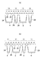
図5(a)(b)はそれぞれ制御電極23に対して制御回路部3から異なる印加パターンで制御電圧+Vを印加した状態(半導体基板に設けた図示しない基板電極と制御電極23との間に制御電圧+Vを印加した状態)を示しており、ポテンシャル井戸24の形状からわかるように、図5(a)では1画素となる2個の感光部11のうち制御電極(1)〜(3)に正の制御電圧+Vを印加するとともに、残りの制御電極(4)〜(6)のうちの中央の制御電極(5)に正の制御電圧+Vを印加している。また、図5(b)では制御電極(1)〜(3)のうちの中央の制御電極(2)に正の制御電圧+Vを印加するとともに、残りの制御電極(4)〜(6)に正の制御電圧+Vを印加している。つまり、1画素を構成する2個の感光部11に印加する制御電圧+Vの印加パターンを交互に入れ換えている。2個の感光部11に印加する制御電圧+Vの印加パターンを入れ換えるタイミングは、変調信号における逆位相の(位相が180度異なる)タイミングになる。なお、各感光部11に設けた3個の制御電極23に同時に制御電圧+Vを印加している期間以外は、各感光部11に設けた中央部の1個の制御電極23(つまり、制御電極(2)(5))にのみ制御電圧+Vを印加し、他の制御電極23は0Vに保つ状態とする。   5A and 5B show a state in which a control voltage + V is applied to the control electrode 23 with a different application pattern from the control circuit unit 3 (between a substrate electrode (not shown) provided on the semiconductor substrate and the control electrode 23). As can be seen from the shape of the potential well 24, in FIG. 5A, the control electrodes (1) to (3) out of the two photosensitive portions 11 serving as one pixel are shown. And a positive control voltage + V is applied to the central control electrode (5) among the remaining control electrodes (4) to (6). In FIG. 5B, a positive control voltage + V is applied to the central control electrode (2) among the control electrodes (1) to (3), and the remaining control electrodes (4) to (6) are applied. A positive control voltage + V is applied. In other words, the application pattern of the control voltage + V applied to the two photosensitive portions 11 constituting one pixel is alternately replaced. The timing of switching the application pattern of the control voltage + V applied to the two photosensitive portions 11 is the timing of the opposite phase (the phase is 180 degrees different) in the modulation signal. In addition, except for the period in which the control voltage + V is simultaneously applied to the three control electrodes 23 provided in each photosensitive portion 11, one central control electrode 23 (that is, the control electrode) provided in each photosensitive portion 11 is provided. (2) The control voltage + V is applied only to (5)), and the other control electrodes 23 are kept at 0V.

たとえば、1画素を構成する2個の感光部11において受光光量A0、A2に対応する電荷を交互に生成する場合は、図2のように、一方の感光部11で受光光量A0に対応する電荷を生成するために3個の制御電極(1)〜(3)に制御電圧+Vを印加している受光期間Twに、他方の感光部11では受光光量A2に対応する電荷を保持するために1個の制御電極(5)にのみ制御電圧+Vを印加する。同様にして、一方の感光部11で受光光量A2に対応する電荷を生成するために3個の制御電極(4)〜(6)に制御電圧+Vを印加している受光期間Twには、他方の感光部11では受光光量A0に対応する電荷を保持するために1個の制御電極(2)にのみ制御電圧+Vを印加する。また、受光光量A0、A2に対応する電荷を生成する受光期間Tw以外の保持期間では制御電極(2)(5)にのみ制御電圧+Vを印加する。図2(b)(c)に受光光量A0、A2に対応する電荷を蓄積する際の各制御電極(1)〜(6)に制御電圧+Vの印加のタイミングを示す。図において斜線部が制御電圧+Vを印加している状態を示し、空白部が制御電極(1)〜(6)に電圧を印加していない状態を示している。   For example, when the charges corresponding to the received light amounts A0 and A2 are alternately generated in the two photosensitive portions 11 constituting one pixel, the charges corresponding to the received light amount A0 in one photosensitive portion 11 as shown in FIG. In the light receiving period Tw in which the control voltage + V is applied to the three control electrodes (1) to (3) in order to generate the voltage, the other photosensitive portion 11 has 1 to hold the charge corresponding to the received light quantity A2. A control voltage + V is applied only to the control electrodes (5). Similarly, in the light receiving period Tw in which the control voltage + V is applied to the three control electrodes (4) to (6) in order to generate a charge corresponding to the received light quantity A2 in one photosensitive portion 11, the other The photosensitive portion 11 applies a control voltage + V only to one control electrode (2) in order to hold a charge corresponding to the received light quantity A0. Further, the control voltage + V is applied only to the control electrodes (2) and (5) in the holding period other than the light receiving period Tw for generating charges corresponding to the received light amounts A0 and A2. FIGS. 2B and 2C show the application timing of the control voltage + V to the control electrodes (1) to (6) when accumulating charges corresponding to the received light amounts A0 and A2. In the figure, the hatched portion indicates a state where the control voltage + V is applied, and the blank portion indicates a state where no voltage is applied to the control electrodes (1) to (6).

1画素を構成する2個の感光部11において受光光量A1、A3に対応する電荷を生成する場合も同様であって、受光光量A0、A2に対応する電荷を生成する場合とは制御電極23に制御電圧+Vを印加するタイミングが、変調信号の位相において90度異なる点が相違するだけである。   The same applies to the case where the charges corresponding to the received light amounts A1 and A3 are generated in the two photosensitive portions 11 constituting one pixel, and the case where the charges corresponding to the received light amounts A0 and A2 are generated is different from the control electrode 23. The only difference is that the timing at which the control voltage + V is applied differs by 90 degrees in the phase of the modulation signal.

受光光量A0、A2に対応する電荷を生成する期間と、受光光量A1、A3に対応する電荷を生成する期間とは、ともに変調信号の1周期分以上(望ましくは複数周期分)の一定期間であり、この期間を検出期間として変調信号の複数周期分の電荷を電荷集積部13に集積する。また、検出期間毎に次の検出期間までの間の期間を読出期間として撮像領域Daから蓄積領域Dbに電荷を転送する。   The period for generating the charges corresponding to the received light amounts A0 and A2 and the period for generating the charges corresponding to the received light amounts A1 and A3 are both fixed periods of one period or more (preferably for a plurality of periods) of the modulation signal. With this period as a detection period, charges for a plurality of periods of the modulation signal are accumulated in the charge accumulation unit 13. In addition, the charge is transferred from the imaging region Da to the storage region Db with the period from the next detection period as the readout period for each detection period.

本実施形態では、受光光量A0に対応する電荷を制御電極(1)〜(3)に対応するポテンシャル井戸24に蓄積するとともに受光光量A2に対応する電荷を制御電極(4)〜(6)に対応するポテンシャル井戸24に蓄積する検出期間を複数回連続して設け、受光光量A1に対応する電荷を制御電極(1)〜(3)に対応するポテンシャル井戸24に蓄積するとともに受光光量A3に対応する電荷を制御電極(4)〜(6)に対応するポテンシャル井戸24に蓄積する検出期間を複数回連続して設けるという動作を繰り返す。つまり、図7に示すように、受光光量A0、A2に対応する電荷を集積する検出期間S11、S12、……と読出期間R11、R12、……とを複数回繰り返す積算期間Paと、受光光量A1、A3に対応する電荷を集積する検出期間S21、S22、……と読出期間R21、R22、……とを複数回繰り返す積算期間Pbとを交互に繰り返し、各積算期間Pa、Pbごとに各受光光量A0、A1、A2、A3に対応する電荷をそれぞれ積算する。位相差ψ(もしくは距離)を求める演算には、変調信号の4つの位相に同期する受光期間Twに相当する電荷が必要であるから、本実施形態では2回の積算期間Pa、Pbにおいてそれぞれ積算した電荷の電荷量を用いて位相差ψ(もしくは距離)の演算を行う。各検出期間S11、S12、……、S21、S22、……においてどの受光光量A0、A1、A2、A3に対応する電荷を電荷集積部13(ポテンシャル井戸24)に対応するかは、制御回路部3が感度制御部13の感度を制御(制御電極23に印加する制御電圧を制御)することによって選択する。なお、積算期間Pa、Pbに積算した電荷量の積算値ではなく平均値を用いて距離を演算してもよい。   In the present embodiment, charges corresponding to the received light amount A0 are accumulated in the potential well 24 corresponding to the control electrodes (1) to (3), and charges corresponding to the received light amount A2 are stored in the control electrodes (4) to (6). The detection period for accumulating in the corresponding potential well 24 is continuously provided a plurality of times, and the charge corresponding to the received light amount A1 is accumulated in the potential well 24 corresponding to the control electrodes (1) to (3) and corresponds to the received light amount A3. The operation of continuously providing a plurality of detection periods for accumulating the charge to be stored in the potential well 24 corresponding to the control electrodes (4) to (6) is repeated. That is, as shown in FIG. 7, the integration period Pa in which the detection periods S11, S12,... And the readout periods R11, R12,. The detection periods S21, S22,... For accumulating charges corresponding to A1 and A3 and the integration period Pb in which the readout periods R21, R22,... Are repeated a plurality of times are alternately repeated, and each of the integration periods Pa and Pb is repeated. Charges corresponding to the received light amounts A0, A1, A2, A3 are integrated. Since calculation for obtaining the phase difference ψ (or distance) requires charges corresponding to the light receiving periods Tw synchronized with the four phases of the modulation signal, in this embodiment, integration is performed in two integration periods Pa and Pb, respectively. The phase difference ψ (or distance) is calculated using the charge amount of the obtained charges. In each detection period S11, S12,..., S21, S22,..., The control circuit unit determines which received light quantity A0, A1, A2, A3 corresponds to the charge integration unit 13 (potential well 24). 3 is selected by controlling the sensitivity of the sensitivity control unit 13 (controlling the control voltage applied to the control electrode 23). Note that the distance may be calculated using an average value instead of the integrated value of the charge amount integrated in the integration periods Pa and Pb.

読出期間R11、R12、……、R21、R22、……には、変調信号の4つの位相に同期する受光期間Twの受光光量A0、A1、A2、A3に対応する電荷を光出力素子1の外部に電気出力として取り出す。取り出した電気出力は画像生成部4において位相差ψの演算に用いられ、結果的に各画素に対応する視線方向に存在する対象物Obまでの距離を求めることが可能になる。   In the readout periods R11, R12,..., R21, R22,..., Charges corresponding to the received light amounts A0, A1, A2, A3 of the light receiving period Tw synchronized with the four phases of the modulation signal are supplied to the light output element 1. Take out to the outside as electrical output. The extracted electrical output is used for the calculation of the phase difference ψ in the image generation unit 4, and as a result, the distance to the object Ob existing in the line-of-sight direction corresponding to each pixel can be obtained.

上述の例では3個の制御電極23((1)〜(3)または(4)〜(6))に同時に印加する制御電圧と、1個の制御電極23((2)または(5))にのみ印加する制御電圧とを等しくしているから、ポテンシャル井戸24の面積は変化するもののポテンシャル井戸24の深さは等しくなっている。この場合、制御電圧を印加していない制御電極23((1)(3)または(4)(6))において生成された電荷は、同程度の確率でポテンシャル井戸24に流れ込む。つまり、感光部11を構成する3個の制御電極23のうちの1個にのみ制御電圧+Vを印加することによって電荷集積部13として機能している領域と、3個の制御電極23のすべてに制御電圧+Vを印加している領域との両方に同程度の量の電荷が流れ込む。つまり、電荷を保持しているポテンシャル井戸24に流れ込む雑音成分が比較的多いものであるから、ダイナミックレンジを低下させる原因になる。   In the above example, the control voltage applied simultaneously to the three control electrodes 23 ((1) to (3) or (4) to (6)) and one control electrode 23 ((2) or (5)) Since the control voltage applied only to is equal, the area of the potential well 24 changes, but the depth of the potential well 24 is equal. In this case, the charges generated at the control electrode 23 ((1) (3) or (4) (6)) to which no control voltage is applied flow into the potential well 24 with a similar probability. That is, by applying the control voltage + V to only one of the three control electrodes 23 constituting the photosensitive portion 11, the region functioning as the charge accumulation portion 13 and all the three control electrodes 23 are applied. A similar amount of charge flows into both the region to which the control voltage + V is applied. That is, since the noise component flowing into the potential well 24 holding the charge is relatively large, the dynamic range is lowered.

そこで、図6のように、演算単位となる2個の感光部11に設けた各3個の制御電極(1)〜(3)または(4)〜(6)に同時に印加する制御電圧が、1個の制御電極(2)または(5)にのみ印加する制御電圧よりも高くなるように設定し、大面積のポテンシャル井戸24を小面積のポテンシャル井戸24よりも深く設定するのが望ましい。このように、主として電荷(電子e)を生成しているポテンシャル井戸24を、主として電荷の保持を行っているポテンシャル井戸24よりも深くすることにより、制御電圧を印加していない制御電極(1)(3)または(4)(6)に対応する部位で生じた電荷は、深いほうのポテンシャル井戸24に流れ込みやすくなる。つまり、制御電極23に一定の制御電圧+Vを印加する場合に比較すると、電荷を保持するポテンシャル井戸24に流れ込む雑音成分を低減することができる。   Therefore, as shown in FIG. 6, the control voltage applied simultaneously to each of the three control electrodes (1) to (3) or (4) to (6) provided in the two photosensitive portions 11 serving as the calculation unit is It is desirable to set the potential well 24 to be higher than the control voltage applied to only one control electrode (2) or (5), and to set the large-area potential well 24 deeper than the small-area potential well 24. As described above, the potential well 24 that mainly generates charges (electrons e) is made deeper than the potential well 24 that mainly holds charges, so that the control electrode (1) to which no control voltage is applied is applied. Charges generated at the sites corresponding to (3) or (4) and (6) are likely to flow into the deeper potential well 24. That is, as compared with the case where a constant control voltage + V is applied to the control electrode 23, the noise component flowing into the potential well 24 holding the charge can be reduced.

上述した例では、各積算期間Pa、Pbにおいて4種類の受光光量A0、A1、A2、A3に対応する電荷を生成する感光部11が決められているから、演算した距離には感光部11の位置の相違による誤差が含まれる可能性がある。とくに、対象物Obに段差があり、受光光量A0と受光光量A2とに対応する感光部11が段差に跨る部位に一致しているとすれば、求められる距離の信頼性が低下することになる。   In the above-described example, the photosensitive unit 11 that generates charges corresponding to the four types of received light amounts A0, A1, A2, and A3 is determined in each integration period Pa and Pb. There may be errors due to position differences. In particular, if there is a step in the object Ob and the photosensitive portion 11 corresponding to the received light amount A0 and the received light amount A2 coincides with the part straddling the step, the reliability of the required distance is lowered. .

この種の問題を解決するには、検出期間ごとに、受光光量A0に対応する電荷を制御電極(1)〜(3)に対応するポテンシャル井戸24に蓄積するとともに受光光量A2に対応する電荷を制御電極(4)〜(6)に対応するポテンシャル井戸24に蓄積する状態と、受光光量A2に対応する電荷を制御電極(1)〜(3)に対応するポテンシャル井戸24に蓄積するとともに受光光量A0に対応する電荷を制御電極(4)〜(6)に対応するポテンシャル井戸24に蓄積する状態と、受光光量A1に対応する電荷を制御電極(1)〜(3)に対応するポテンシャル井戸24に蓄積するとともに受光光量A3に対応する電荷を制御電極(4)〜(6)に対応するポテンシャル井戸24に蓄積する状態と、受光光量A3に対応する電荷を制御電極(1)〜(3)に対応するポテンシャル井戸24に蓄積するとともに受光光量A1に対応する電荷を制御電極(4)〜(6)に対応するポテンシャル井戸24に蓄積する状態との4状態を循環的に切り換えればよい。つまり、各検出期間ごとに、各電荷集積部13にそれぞれ集積する電荷を各受光光量A0、A1、A2、A3に対応する電荷から循環的に選択するのである。この動作を繰り返すことによって、4種類の受光期間Twの受光光量A0、A1、A2、A3に対応する電荷を4回の整数倍の読出動作で光出力素子1の外部に電気出力として取り出すことができる。   In order to solve this type of problem, the charge corresponding to the received light amount A0 is accumulated in the potential well 24 corresponding to the control electrodes (1) to (3) and the charge corresponding to the received light amount A2 is detected for each detection period. The state of accumulation in the potential well 24 corresponding to the control electrodes (4) to (6) and the charge corresponding to the received light amount A2 are accumulated in the potential well 24 corresponding to the control electrodes (1) to (3) and the received light amount. A state in which charges corresponding to A0 are accumulated in the potential well 24 corresponding to the control electrodes (4) to (6), and a charge corresponding to the received light amount A1 is potential well 24 corresponding to the control electrodes (1) to (3). In the potential well 24 corresponding to the control electrodes (4) to (6) and the charge corresponding to the received light amount A3. Circulates four states including the state in which the potential well 24 corresponding to (1) to (3) is accumulated and the charge corresponding to the received light quantity A1 is accumulated in the potential well 24 corresponding to the control electrodes (4) to (6). Can be switched. That is, for each detection period, the charges accumulated in each charge accumulation unit 13 are cyclically selected from the charges corresponding to the respective received light amounts A0, A1, A2, A3. By repeating this operation, the charges corresponding to the received light amounts A0, A1, A2, and A3 in the four types of light receiving periods Tw can be taken out as an electrical output to the outside of the light output element 1 by the reading operation of an integral multiple of four times. it can.

さらに詳しく説明すると、画像生成部4では、図8(a)に示すように、検出期間S1、S2、S3、S4ごとに設けた読出期間R1、R2、R3、R4において変調信号の2つの異なる位相に同期した受光期間Twに相当する電気出力が光検出素子1から与えられる。位相差ψ(もしくは距離)を求める演算には、すべての位相の受光期間Twに相当する電気出力が必要であるから、検出期間S1、S2、S3、S4の4回分の電気出力を用いて位相差ψ(もしくは距離)の演算を行う。図示例では、4回の検出期間S1、S2、S3、S4および読出期間R1、R2、R3、R4の期間P1で対象物Obまでの距離が得られるから、期間P1は画像の1フレーム分の時間に相当する。   More specifically, as shown in FIG. 8A, the image generation unit 4 uses two different modulation signals in the readout periods R1, R2, R3, and R4 provided for each of the detection periods S1, S2, S3, and S4. An electrical output corresponding to the light receiving period Tw synchronized with the phase is given from the light detection element 1. Since the calculation for obtaining the phase difference ψ (or distance) requires an electrical output corresponding to the light receiving period Tw of all phases, the electric output corresponding to the four detection periods S1, S2, S3, and S4 is used. The phase difference ψ (or distance) is calculated. In the illustrated example, since the distance to the object Ob is obtained in the period P1 of the four detection periods S1, S2, S3, S4 and the readout periods R1, R2, R3, R4, the period P1 corresponds to one frame of the image. It corresponds to time.

上述した期間P1には、図8(b)に示すように、受光光量A0、A2に相当する電気出力が得られる2回の検出期間S1、S2と、受光光量A1、A3に相当する電気出力が得られる2回の検出期間S3、S4とが含まれており、受光光量A0、A2に相当する電気出力が得られる2回の検出期間S1、S2ではそれぞれの受光光量A0、A2が得られた感光部11が入れ代わり、また、受光光量A1、A3に相当する電気出力が得られる2回の検出期間S3、S4ではそれぞれの受光光量A1、A3が得られた感光部11が入れ代わる。そこで、受光光量A0、A2に相当する電気出力が得られる2回の検出期間S1、S2において得られた電気出力の積算値(または平均値)を受光光量A0、A2ごとに求め、また、受光光量A1、A3に相当する電気出力が得られる2回の検出期間S3、S4において得られた電気出力の積算値(または平均値)を受光光量A1、A3ごとに求めて、4個の積算値(または平均値)をそれぞれ受光光量A0、A1、A2、A3に相当する値に用いて(1)式の演算を行う。このような演算により、各受光光量A0、A1、A2、A3に対応した電気出力を得る際の感光部11の位置のずれによる距離測定の信頼性の低下を低減することができる。   In the above-described period P1, as shown in FIG. 8B, two detection periods S1 and S2 in which electrical outputs corresponding to the received light amounts A0 and A2 are obtained, and electrical outputs corresponding to the received light amounts A1 and A3. Are included in two detection periods S3 and S4, and in the two detection periods S1 and S2 in which electrical outputs corresponding to the received light amounts A0 and A2 are obtained, the received light amounts A0 and A2 are obtained. In addition, the photosensitive portion 11 having the respective received light amounts A1 and A3 is replaced in two detection periods S3 and S4 in which electrical outputs corresponding to the received light amounts A1 and A3 are obtained. Therefore, the integrated value (or average value) of the electrical outputs obtained in the two detection periods S1 and S2 in which the electrical outputs corresponding to the received light amounts A0 and A2 are obtained is obtained for each received light amount A0 and A2. The integrated value (or average value) of the electrical outputs obtained in the two detection periods S3 and S4 in which the electrical outputs corresponding to the light amounts A1 and A3 are obtained is obtained for each received light amount A1 and A3, and four integrated values are obtained. (Or average value) is used as values corresponding to the received light amounts A0, A1, A2, and A3, respectively, and the calculation of equation (1) is performed. By such calculation, it is possible to reduce a decrease in reliability of distance measurement due to a shift in the position of the photosensitive portion 11 when obtaining an electric output corresponding to each of the received light amounts A0, A1, A2, and A3.

なお、上述した距離画像センサの構成例では、受光光量A0、A1、A2、A3に対応する4つの受光期間Twを変調信号の1周期内で位相の間隔が90度ずつになるように設定しているが、変調信号に対する位相が既知であれば4つの受光期間Twは90度以外の適宜の間隔で設定することが可能である。ただし、間隔が異なれば位相差ψを求める算式は異なる。また、4つの受光期間Twの受光光量に対応した電荷(電気出力)を取り出す周期は、対象物Obの反射率および外光成分が変化せず、かつ位相差ψも変化しない時間内であれば、変調信号の1周期内で4種類の電気出力を取り出すことも必須ではない。さらに、太陽光や照明光のような外乱光の影響があるときには、発光源2から放射される光の波長のみを透過させる光学フィルタを感光部11の前に配置するのが望ましい。図5、図6を用いて説明した構成例では、感光部11ごとに3個ずつの制御電極23を対応付けているが、制御電極23を4個以上設けるようにしてもよい。また、上述の例ではFT方式のCCDイメージセンサと同様の構成を採用しているが、インターライン・トランスファ(IT)方式、フレーム・インターライン・トランスファ(FIT)方式と同様の構成を採用することも可能である。   In the configuration example of the distance image sensor described above, the four light receiving periods Tw corresponding to the received light amounts A0, A1, A2, and A3 are set so that the phase interval is 90 degrees in one cycle of the modulation signal. However, if the phase with respect to the modulation signal is known, the four light receiving periods Tw can be set at appropriate intervals other than 90 degrees. However, the formula for obtaining the phase difference ψ differs if the interval is different. In addition, the period for taking out the electric charges (electrical output) corresponding to the received light amounts in the four light receiving periods Tw is within a time period in which the reflectance and the external light component of the object Ob do not change and the phase difference ψ does not change. It is not essential to extract four types of electrical outputs within one period of the modulation signal. Furthermore, when there is an influence of disturbance light such as sunlight or illumination light, it is desirable to dispose an optical filter that transmits only the wavelength of light emitted from the light source 2 in front of the photosensitive portion 11. In the configuration example described with reference to FIGS. 5 and 6, three control electrodes 23 are associated with each photosensitive portion 11, but four or more control electrodes 23 may be provided. In the above example, the same configuration as the FT type CCD image sensor is adopted, but the same configuration as the interline transfer (IT) method and the frame interline transfer (FIT) method is adopted. Is also possible.

上述した構成例では、光検出素子1において垂直方向に配列した各2個ずつの感光部11を演算単位とし、光検出素子1から感光部11の電気出力を1回読み出す検出期間においては、演算単位となる2個の感光部11において受光光量A0、A2または受光光量A1、A3に相当する電気出力が得られるように制御回路部3において各感光部11の受光期間Twを制御している。言い換えると、変調信号における規定の位相に同期して設定された4つの受光期間Twのうちの2つの受光期間Twの電気出力を一括して読み出している。この構成に対して、垂直方向に配列した各4個ずつの感光部11を演算単位とし、変調信号の位相に同期して設定された4つの受光期間Twの電気出力が演算単位となる各感光部11で得られるように感光部11の受光期間Twを制御することも可能である。この場合には、受光光量A0、A1、A2、A3に対応する4つの受光期間Twの電気出力を1回の検出期間で読み出すことができる。   In the configuration example described above, in the detection period in which each of the two photosensitive units 11 arranged in the vertical direction in the light detection element 1 is used as a calculation unit, and the electrical output of the photosensitive unit 11 is read once from the light detection element 1, the calculation is performed. The light receiving period Tw of each photosensitive unit 11 is controlled in the control circuit unit 3 so that the two photosensitive units 11 serving as a unit can obtain electric outputs corresponding to the received light amounts A0 and A2 or the received light amounts A1 and A3. In other words, the electrical outputs of two light receiving periods Tw out of the four light receiving periods Tw set in synchronization with the prescribed phase in the modulation signal are collectively read out. In contrast to this configuration, each of the four photosensitive sections 11 arranged in the vertical direction is used as a calculation unit, and each of the photosensitive units whose electric outputs in four light receiving periods Tw set in synchronization with the phase of the modulation signal are used as a calculation unit. It is also possible to control the light receiving period Tw of the photosensitive portion 11 as obtained by the portion 11. In this case, the electric outputs of the four light receiving periods Tw corresponding to the received light amounts A0, A1, A2, A3 can be read out in one detection period.

また、上述した構成例では、光検出素子1から得られる受光光量A0、A1、A2、A3に対応した電気出力の積算値または平均値を求め、この値を用いて各画素の画素値である距離を求めているが、画像生成部4では検出期間毎に各感光部11ごとの電気出力が入力され、電気出力を平均しなければ各1個の感光部11において距離を求めるのに必要な受光光量A0、A1、A2、A3に相当する4種類の電気出力が得られるから、この4種類の電気出力を用いて対象物Obまでの距離を求めることも可能である。さらに、光検出素子1で受光する受光光量の変化幅は、外乱光に時間変化がなければ、発光源2から対象空間に照射される光の強度変調の振幅よりも小さくなる。そこで、常時は演算単位となる感光部11の電気出力を組み合わせて上述のようにして距離を求め、距離を求めるために演算単位としている感光部11で受光した受光光量A0、A1、A2、A3の変化幅(最大値と最小値との差)が、予想された変化幅よりも大きいときに異常値と判断し、異常値であれば1個の感光部11から得られる電気信号のみを用いて距離を求めるようにすることも可能である。 In the configuration example described above, the integrated value or average value of the electrical outputs corresponding to the received light amounts A0, A1, A2, and A3 obtained from the light detection element 1 is obtained, and this value is used as the pixel value of each pixel. Although the distance is obtained, the image generation unit 4 receives the electrical output of each photosensitive unit 11 for each detection period, and if the electrical output is not averaged, it is necessary to obtain the distance in each one photosensitive unit 11. Since four types of electrical outputs corresponding to the received light amounts A0, A1, A2, and A3 are obtained, the distance to the object Ob can be obtained using these four types of electrical outputs. Further, the amount of change in the amount of received light received by the light detection element 1 is smaller than the amplitude of the intensity modulation of the light emitted from the light source 2 to the target space if the disturbance light does not change with time. Therefore, the distance is obtained as described above by combining the electrical outputs of the photosensitive unit 11 which is a calculation unit at all times, and the received light amounts A0, A1, A2, A3 received by the photosensitive unit 11 which is the calculation unit in order to obtain the distance. Is determined to be an abnormal value when the change width (the difference between the maximum value and the minimum value) is larger than the expected change width, and if it is an abnormal value, only an electric signal obtained from one photosensitive portion 11 is used. It is also possible to obtain the distance.

本発明の実施形態を示すブロック図である。It is a block diagram which shows embodiment of this invention. 同上の動作説明図である。It is operation | movement explanatory drawing same as the above. 同上に用いる光検出素子の要部の動作説明図である。It is operation | movement explanatory drawing of the principal part of the photon detection element used for the same as the above. 同上に用いる光検出素子の平面図である。It is a top view of the photon detection element used for the same as the above. 同上に用いる光検出素子の要部の動作説明図である。It is operation | movement explanatory drawing of the principal part of the photon detection element used for the same as the above. 同上に用いる光検出素子の要部の動作説明図である。It is operation | movement explanatory drawing of the principal part of the photon detection element used for the same as the above. 同上の動作説明図である。It is operation | movement explanatory drawing same as the above. 同上の他の動作例の動作説明図である。It is operation | movement explanatory drawing of the other operation example same as the above.

符号の説明Explanation of symbols

1 光検出素子
2 発光源
3 制御回路部
4 画像生成部
5 受光光学系
11 感光部
Ob 対象物
DESCRIPTION OF SYMBOLS 1 Photodetector 2 Light emission source 3 Control circuit part 4 Image generation part 5 Light reception optical system 11 Photosensitive part Ob Object

Claims (2)

所定周期の変調信号で強度変調された光を対象空間に照射する発光源と、対象空間からの光を受光してそれぞれ受光光量に応じた電荷を生成する複数個の感光部を有し対象空間を撮像する光検出素子と、各感光部が対象空間からの光を受光する受光期間を制御する制御回路部と、感光部で生成された電荷を用いて対象物までの距離を求めこの距離を画素値とする距離画像を生成する画像生成部とを備え、受光期間は、変調信号の位相に同期しかつ変調信号の周期よりも短く設定され、光検出素子は、複数個隣接した感光部を演算単位とし、複数の受光期間で得られる電荷を変調信号の1周期以上の期間である検出期間ごとに集積した電荷を画像生成部に与え、かつ演算単位となる各感光部の受光期間を、検出期間毎に前記位相のうちの異なる位相の受光期間に変更するように電荷の転送タイミングが制御回路部で制御され、画像生成部は、複数の検出期間の電荷量を受光期間別に積算した電荷量を用いて距離を求め、当該距離を距離画像の画素値とすることを特徴とする距離画像センサ。 A target space having a light emitting source that irradiates the target space with light whose intensity is modulated with a modulation signal of a predetermined period, and a plurality of photosensitive units that receive light from the target space and generate charges corresponding to the amount of received light, respectively. A light detection element that captures the light, a control circuit unit that controls a light receiving period in which each photosensitive unit receives light from the target space, and a distance to the target using the charge generated by the photosensitive unit. An image generation unit that generates a distance image as a pixel value, the light receiving period is set to be shorter than the period of the modulation signal in synchronization with the phase of the modulation signal, and the light detection element includes a plurality of adjacent photosensitive units. The calculation unit is a charge obtained by accumulating charges obtained in a plurality of light receiving periods for each detection period which is a period of one or more periods of the modulation signal , and the light receiving period of each photosensitive unit serving as a calculation unit is given as Different of the phases for each detection period Transfer timing of the charge so as to change the light receiving period for the phase are controlled by the control circuit unit, the image generating unit obtains a distance using the amount of charge accumulated by the light receiving period the amount of charge of a plurality of detection periods, the distance distance image sensor, characterized in that the pixel values of the distance image. 記画像生成部は、演算単位となる前記各感光部で得られた電荷を積算する複数の検出期間において、各検出期間ごとの受光期間の回数を同回数ずつとすることを特徴とする請求項1記載の距離画像センサ。 Before Symbol image generation unit, in a plurality of detection periods for accumulating charges obtained by the respective photosensitive portions serving as operation unit, wherein, characterized in that the in equal number to the number of the light receiving period for each detection period Item 1. The distance image sensor according to item 1.
JP2004272000A 2004-09-17 2004-09-17 Distance image sensor Expired - Fee Related JP3906858B2 (en)

Priority Applications (9)

Application Number Priority Date Filing Date Title
JP2004272000A JP3906858B2 (en) 2004-09-17 2004-09-17 Distance image sensor
AT05785265T ATE392628T1 (en) 2004-09-17 2005-09-16 RANGE IMAGE SENSOR
TW094132101A TWI280042B (en) 2004-09-17 2005-09-16 A range image sensor
KR1020067006103A KR100778904B1 (en) 2004-09-17 2005-09-16 A range image sensor
US10/573,573 US7362419B2 (en) 2004-09-17 2005-09-16 Range image sensor
DE602005006080T DE602005006080T2 (en) 2004-09-17 2005-09-16 Range image sensor
PCT/JP2005/017569 WO2006030989A1 (en) 2004-09-17 2005-09-16 A range image sensor
EP05785265A EP1668384B1 (en) 2004-09-17 2005-09-16 A range image sensor
HK06108592A HK1088394A1 (en) 2004-09-17 2006-08-03 A range image sensor

Applications Claiming Priority (1)

Application Number Priority Date Filing Date Title
JP2004272000A JP3906858B2 (en) 2004-09-17 2004-09-17 Distance image sensor

Publications (3)

Publication Number Publication Date
JP2006084429A JP2006084429A (en) 2006-03-30
JP2006084429A5 JP2006084429A5 (en) 2006-09-14
JP3906858B2 true JP3906858B2 (en) 2007-04-18

Family

ID=36163040

Family Applications (1)

Application Number Title Priority Date Filing Date
JP2004272000A Expired - Fee Related JP3906858B2 (en) 2004-09-17 2004-09-17 Distance image sensor

Country Status (1)

Country Link
JP (1) JP3906858B2 (en)

Cited By (3)

* Cited by examiner, † Cited by third party
Publication number Priority date Publication date Assignee Title
JP2011122913A (en) * 2009-12-10 2011-06-23 Stanley Electric Co Ltd Distance image generation apparatus and distance image generation method
JPWO2010100846A1 (en) * 2009-03-05 2012-09-06 パナソニック株式会社 Distance measuring device, distance measuring method, program, and integrated circuit
JP2014169921A (en) * 2013-03-04 2014-09-18 Denso Corp Distance sensor

Families Citing this family (10)

* Cited by examiner, † Cited by third party
Publication number Priority date Publication date Assignee Title
US7362419B2 (en) 2004-09-17 2008-04-22 Matsushita Electric Works, Ltd. Range image sensor
EP1944622B1 (en) 2006-10-18 2013-04-10 Panasonic Corporation Spatial information detecting device
JP4971744B2 (en) * 2006-10-18 2012-07-11 パナソニック株式会社 Spatial information detector using intensity-modulated light
JP5222000B2 (en) * 2007-03-30 2013-06-26 パナソニック株式会社 Image sensor
JP5448617B2 (en) 2008-08-19 2014-03-19 パナソニック株式会社 Distance estimation device, distance estimation method, program, integrated circuit, and camera
JP5476190B2 (en) 2010-03-31 2014-04-23 本田技研工業株式会社 Solid-state imaging device
KR101669412B1 (en) 2010-11-01 2016-10-26 삼성전자주식회사 Method and apparatus of measuring depth information for 3d camera
JP5774512B2 (en) 2012-01-31 2015-09-09 株式会社東芝 Ranging device
JP6025081B2 (en) * 2013-02-28 2016-11-16 株式会社テクノロジーハブ Distance image sensor
JP2014196963A (en) * 2013-03-29 2014-10-16 日本信号株式会社 Distance image processing system

Cited By (5)

* Cited by examiner, † Cited by third party
Publication number Priority date Publication date Assignee Title
JPWO2010100846A1 (en) * 2009-03-05 2012-09-06 パナソニック株式会社 Distance measuring device, distance measuring method, program, and integrated circuit
US8531651B2 (en) 2009-03-05 2013-09-10 Panasonic Corporation Distance measuring device, distance measuring method, program, and integrated circuit
JP5584196B2 (en) * 2009-03-05 2014-09-03 パナソニック インテレクチュアル プロパティ コーポレーション オブ アメリカ Distance measuring device, distance measuring method, program, and integrated circuit
JP2011122913A (en) * 2009-12-10 2011-06-23 Stanley Electric Co Ltd Distance image generation apparatus and distance image generation method
JP2014169921A (en) * 2013-03-04 2014-09-18 Denso Corp Distance sensor

Also Published As

Publication number Publication date
JP2006084429A (en) 2006-03-30

Similar Documents

Publication Publication Date Title
US7362419B2 (en) Range image sensor
JP3906859B2 (en) Distance image sensor
KR102494430B1 (en) System and method for determining distance to object
KR102471540B1 (en) Method for subtracting background light from exposure values of pixels in an imaging array and pixels using the same
EP3365700B1 (en) System and method for determining a distance to an object
JP4363296B2 (en) Distance image sensor
JP4466260B2 (en) Image processing device
US20200124726A1 (en) System and method for determining a distance to an object
US11029391B2 (en) System for determining a distance to an object
JP3906858B2 (en) Distance image sensor
JP2008209162A (en) Range image sensor
JP2004309310A (en) Sensitivity control method for photo detector and detection device of space information using intensity modulation light
JP2006185166A (en) Human detection method and human detector using depth map
JP4543904B2 (en) Distance image sensor
JP4259418B2 (en) Image processing device
JP4432744B2 (en) Image processing device
JP2006048156A (en) Image processor
JP2006053791A (en) Image processor
JP4270067B2 (en) Image processing device

Legal Events

Date Code Title Description
A521 Request for written amendment filed

Free format text: JAPANESE INTERMEDIATE CODE: A523

Effective date: 20060727

A131 Notification of reasons for refusal

Free format text: JAPANESE INTERMEDIATE CODE: A131

Effective date: 20061003

A521 Request for written amendment filed

Free format text: JAPANESE INTERMEDIATE CODE: A523

Effective date: 20061204

TRDD Decision of grant or rejection written
A01 Written decision to grant a patent or to grant a registration (utility model)

Free format text: JAPANESE INTERMEDIATE CODE: A01

Effective date: 20061226

A61 First payment of annual fees (during grant procedure)

Free format text: JAPANESE INTERMEDIATE CODE: A61

Effective date: 20070108

FPAY Renewal fee payment (event date is renewal date of database)

Free format text: PAYMENT UNTIL: 20100126

Year of fee payment: 3

S533 Written request for registration of change of name

Free format text: JAPANESE INTERMEDIATE CODE: R313533

FPAY Renewal fee payment (event date is renewal date of database)

Free format text: PAYMENT UNTIL: 20100126

Year of fee payment: 3

R350 Written notification of registration of transfer

Free format text: JAPANESE INTERMEDIATE CODE: R350

FPAY Renewal fee payment (event date is renewal date of database)

Free format text: PAYMENT UNTIL: 20100126

Year of fee payment: 3

FPAY Renewal fee payment (event date is renewal date of database)

Free format text: PAYMENT UNTIL: 20110126

Year of fee payment: 4

FPAY Renewal fee payment (event date is renewal date of database)

Free format text: PAYMENT UNTIL: 20120126

Year of fee payment: 5

FPAY Renewal fee payment (event date is renewal date of database)

Free format text: PAYMENT UNTIL: 20120126

Year of fee payment: 5

FPAY Renewal fee payment (event date is renewal date of database)

Free format text: PAYMENT UNTIL: 20130126

Year of fee payment: 6

FPAY Renewal fee payment (event date is renewal date of database)

Free format text: PAYMENT UNTIL: 20130126

Year of fee payment: 6

LAPS Cancellation because of no payment of annual fees