JP3899994B2 - Image signal processing apparatus and image signal processing method - Google Patents
Image signal processing apparatus and image signal processing method Download PDFInfo
- Publication number
- JP3899994B2 JP3899994B2 JP2002118278A JP2002118278A JP3899994B2 JP 3899994 B2 JP3899994 B2 JP 3899994B2 JP 2002118278 A JP2002118278 A JP 2002118278A JP 2002118278 A JP2002118278 A JP 2002118278A JP 3899994 B2 JP3899994 B2 JP 3899994B2
- Authority
- JP
- Japan
- Prior art keywords
- image signal
- interpolation
- image
- processing
- circuit
- Prior art date
- Legal status (The legal status is an assumption and is not a legal conclusion. Google has not performed a legal analysis and makes no representation as to the accuracy of the status listed.)
- Expired - Fee Related
Links
- 238000003672 processing method Methods 0.000 title claims description 19
- 238000000034 method Methods 0.000 claims description 52
- 238000004364 calculation method Methods 0.000 claims description 14
- 238000006243 chemical reaction Methods 0.000 claims description 10
- 239000000872 buffer Substances 0.000 description 18
- 238000010586 diagram Methods 0.000 description 15
- 102100037009 Filaggrin-2 Human genes 0.000 description 4
- 101000878281 Homo sapiens Filaggrin-2 Proteins 0.000 description 4
- 238000012888 cubic function Methods 0.000 description 2
- 230000003044 adaptive effect Effects 0.000 description 1
- 238000001514 detection method Methods 0.000 description 1
- 230000000694 effects Effects 0.000 description 1
- 239000004973 liquid crystal related substance Substances 0.000 description 1
- 238000005457 optimization Methods 0.000 description 1
Images


Classifications
-
- G—PHYSICS
- G06—COMPUTING; CALCULATING OR COUNTING
- G06T—IMAGE DATA PROCESSING OR GENERATION, IN GENERAL
- G06T3/00—Geometric image transformation in the plane of the image
- G06T3/40—Scaling the whole image or part thereof
- G06T3/4007—Interpolation-based scaling, e.g. bilinear interpolation
Description
【0001】
【発明の属する技術分野】
本発明は、画像信号処理装置及び画像信号処理方法における画像信号の拡大または縮小を行うことにより画像の解像度を変換する画像変換装置及び画像信号処理方法に関するものである。
【0002】
【従来の技術】
従来、画像信号処理装置に用いられる画素数変換回路は、LCD(Liquid Crystal Display)やPDP(Plasma Display Panel)のような固定画素表示装置で様々な表示フォーマットを持つ入力信号を表示するために用いられていた。
【0003】
近年、BS(Broadcast satelite: 放送衛星)ディジタル放送の開始に伴い、テレビ放送の自然画とデータ放送のテキスト(文字)やCG(Computer Graphic)が混在する画像信号に対して、これらの画像を前述の固定画素表示装置に高画質で表示することが要求されている。
【0004】
この要求に応えるべく、これまでに画素数変換のため種々の画像信号処理方法が提案されている。例えば、特許文献である特開平11−055503号公報に開示されているように自然画と文字に対する補間処理回路を別々に持ち、これを適宜切り替えることが提案されている。
同公報によれば、解像度変換の比を整数比M:N(ここで、MとNは整数である)として元の画像をM×M画素の細分化領域に分割し、この中に含まれている画素の色成分の種類があるしきい値以上であれば、自然画と判断して線形補間回路で画像を処理し、上記しきい値以下であれば、文字かCGと判断して上記細分化されたM×Mの画素領域ごとの相関係数に応じた適応間引き処理回路で画像処理を行って、N×N画素に縮小することが記載されている。
【0005】
また、特許文献である特開2001−189850号公報に開示されているように、自然画とCGとで補間特性を適宜切り替えることが提案されている。
同公報によれば、画像の解像度を変換する画像処理装置における解像度変換装置において、文字及び自然画が混在する画像信号から文字か自然画かを判別する画像性質検出回路と、上記文字か自然画化の判別に基づいてキュービック(Cubic )コンボリューション(畳み込み)方式により補間関数を発生する補間関数発生回路と、上記補間関数発生回路から出力された補間関数に基づき上記画像信号を縮小または拡大する解像度変換を行う解像度変換回路とを具備することが記載されている。
【0006】
【発明が解決しようとする課題】
ところで、上述した従来の画像処理方式では、画像種類の認識及び補間処理の最適化に問題がある。例えば、特開平11−055503号公報に開示された手法では、色成分が多く含まれているテキストなどはCG画像と認識できないことや、最近傍補間と線形補間の2系統の回路を持つ必要があることや線形補間では自然画部分の変換に関して高画質化要求には応えられない。
【0007】
また、特開2001−189850号公報に開示された手法では、キュービックコンボリューション方式の特性が適宜切り換えられているが、キュービックコンボリューション方式はCG画像の補間処理には最適ではないため、高画質化の要求には応えられないという不利益がある。
【0008】
本発明は、かかる事情に鑑みてなされたものであり、その目的は、画像信号の種類について高精度で判別し、当該判別の結果に従って1つの補間処理回路によってそれぞれの画像種類に対応する複数の補間方式を切り換えて画素数変換処理を行うことができ、回路構成の簡素化を実現しながら、高画質化の要求に対応できる画像信号処理装置を提供することにある。また、高画質化の要求に対応できる画像信号処理方法を提供することである。
【0009】
上記目的を達成するため、本発明の画像信号処理装置は、入力される画像信号に応じて、当該画像信号が自然画の画像信号か、コンピュータによって生成されたコンピュータ画像信号かを判別する画像判別手段と、上記画像判別手段の判別結果に応じて、所定の補間処理を選択し、選択された補間処理で上記入力画像信号に対して処理を行い、画素数変換を行う補間処理手段とを有する画像信号処理装置であって、上記画像判別手段は、上記入力される画像信号の隣接する第1、第2、第3及び第4の4つの画素のデータを用いて、上記第1と第2の画素データの差の絶対値と上記第3と第4の画素データの差の絶対値との和と、上記第2と第3の画素データの差の絶対値との比を算出し、当該算出した比と所定のしきい値との比較結果に基づき、上記入力される画像信号が自然画の画像信号か、コンピュータ画像信号かについて判別する。
【0010】
また、本発明では、好適には、上記画像判別手段は、上記入力される画像信号の隣接する画素データを用いて所定の演算を行い、当該演算の結果に基づき上記入力される画像信号が自然画の画像信号か、コンピュータ画像信号かについて判別する。
【0011】
また、本発明では、好適には、上記補間処理手段は、上記画像判別手段の判別結果に基づき、線形補間とキュービック補間とを切り換えて、上記入力される画像信号に対して補間処理を行い、また、上記画像判別手段の判別結果に基づき、最近傍補間とキュービック補間とを切り換えて、上記入力される画像信号に対して補間処理を行う。
【0012】
また、本発明では、好適には、上記補間処理手段は、上記画像判別手段の判別結果に基づき、線形補間、最近傍補間とキュービック補間とを切り換えて、上記入力される画像信号に対して補間処理を行う。
【0013】
また、本発明では、好適には、上記画像判別手段は、上記入力される画像信号における隣接する画素の輝度を表す輝度データに基づき、上記演算を行い、当該演算結果に基づき上記入力される画像信号を判別する。
【0014】
また、本発明では、好適には、上記補間処理手段は、上記輝度データに基づいた判別結果に基づき、補間処理を切り換えて、上記入力される画像信号の色差信号に対して補間処理を行う。
【0015】
また、本発明では、好適には、上記画像判別手段は、上記入力される画像信号に対して、水平方向と垂直方向においてそれぞれ上記判別を行う。さらに、上記補間処理手段は、上記水平方向と垂直方向それぞれの判別結果に応じて、水平方向と垂直方向にそれぞれにおいて上記補間処理を行う。
【0016】
本発明の画像信号処理方法は、入力される画像信号に応じて、当該画像信号が自然画の画像信号か、コンピュータによって生成されたコンピュータ画像信号かを判別する画像判別ステップと、上記画像判別ステップの判別結果に応じて、所定の補間処理を選択し、選択された補間処理で上記入力画像信号に対して処理を行い、画素数変換を行う補間処理ステップとを有する画像信号処理方法であって、上記画像判別ステップは、上記入力される画像信号の隣接する第1、第2、第3及び第4の4つの画素のデータを用いて、上記第1と第2の画素データの差の絶対値と上記第3と第4の画素データの差の絶対値との和と、上記第2と第3の画素データの差の絶対値との比を算出し、当該算出した比と所定のしきい値との比較結果に基づき、上記入力される画像信号が自然画の画像信号か、コンピュータ画像信号かについて判別する。
【0017】
本発明によれば、画像判別手段によって、入力画像信号における隣接する画素データに基づき、所定の演算を行いその結果に基づき、入力画像信号の種類を判別する。当該判別結果に応じて、補間処理手段は、入力画像信号の種類に適した補間処理方式を適宜切り換えて、補間処理を行い、画素数の変換を行う。これによって、画像信号の種類に適した補間処理方式で補間処理が行われ、画素数変換が行われる。また、補間処理手段は、1つの回路で複数の異なる補間処理を実現できるため、回路構成が簡略化される。
【0018】
【発明の実施の形態】
図1は本発明に係る画像信号処理装置の一実施形態を示す構成図である。
図示のように、本実施形態の画像処理装置は、垂直用補間回路10、垂直用画像判別回路20、ラインバッファ30−1,30−2,30−3、水平用補間回路50、水平用画像判別回路60、及び画素バッファ70−1,70−2,70−3によって構成されている。
以下、本実施形態の画像信号処理装置の各部分回路の構成について説明する。
【0019】
垂直用補間回路10は、垂直用画像判別回路20の判別結果を示すフラグ信号FLGy に従って、垂直方向における最適な補間処理方式を選択し、選択された補間方式に基づいて、入力された垂直方向に隣り合う4つの画素の画素データDy ,By ,Ay ,Cy に対して垂直方向に補間処理を行い、画素数変換を行う。
【0020】
垂直用画像判別回路20は、入力された垂直方向に隣り合う4つの画素の画素データDy ,By ,Ay ,Cy に基づき、入力される画像信号Sinの種類を判別し、当該判別の結果、画像信号の種類を示すフラグ信号FLGy を出力する。
【0021】
ラインバッファ30−1,30−2及び30−3は、直列に接続されている。これらのラインバッファは、例えば、直列接続されている複数段のシフトレジスタなどによって構成され、それぞれ1ライン分の画素データを記憶し、記憶されている画素データを入力段から出力段に向けて順次転送する。このため、各ラインバッファの出力段から出力される画素データが、入力段に入力される画素データに対して1ライン分前の画素データとなる。即ち、図1において、ラインバッファ30−3から出力される画素データCy は、ラインバッファ30−2から出力される画素データAy より1ライン分前の画素データであり、同様に、ラインバッファ30−1から出力される画素データBy は、現在入力される画素データDy より1ライン分前の画素データである。
【0022】
上述した垂直用補間回路10によって垂直方向に補間処理された画素データDX が水平用補間回路50、水平用画像判別回路60及び画素バッファ70−1にそれぞれ入力される。
【0023】
水平用補間回路50は、水平用画像判別回路60の判別結果を示すフラグ信号FLGx に従って、水平方向における最適な補間処理方式を選択し、選択された補間方式に基づいて、入力された水平方向に隣り合う4つの画素の画素データDx ,Bx ,Ax ,Cx に対して水平方向補間処理を行い、画素数変換を行う。
【0024】
水平用画像判別回路60は、入力された水平方向に隣り合う4つの画素の画素データDx ,Bx ,Ax ,Cx に基づき、画像信号の種類を判別し、判別の結果、画像信号の種類を示すフラグ信号FLGx を出力する。
【0025】
画素バッファ70−1,70−2,70−3は、それぞれ1画素分の画素データを保持するシフトレジスタによって構成されている。これらの画素バッファは直列に接続されて、それぞれ1画素分の画素データを記憶し、記憶されている画素データを次の画素バッファに転送する。このため、各画素バッファから出力される画素データが入力される画素データに対して、時間軸上1つ前の画素の画素データとなる。例えば、画素バッファ70−3から出力される画素データCx は、画素バッファ70−2から出力される画素データAx より1つ前の画素の画素データであり、同様に、画素バッファ70−1から出力される画素データBx は、入力画素データDx に比べて、1つ前の画素の画素データとなる。
【0026】
次に、本実施形態の画像信号処理装置における画像判別処理及び画像補間処理について説明する。
【0027】
画像判別処理
まず、画像信号の判別処理について説明する。判別処理は、入力される画像信号がコンピュータ画像信号であるか、自然画の画像信号であるかについて判別する。判別処理はそれぞれ垂直と水平方向において行われる。垂直方向の判別は、図1に示す垂直用画像判別回路20によって行われ、水平方向の判別は、水平用画像判別回路60によって行われる。なお、垂直と水平方向の判別処理は、ほぼ同じであるので、以下、特に垂直または水平の処理を区別せず、入力される4つの隣接画素の画素データをA,B,C,Dとして、画像判別処理について説明する。
【0028】
なお、ここで、4つの隣接画素の画素データが時間軸上C,A,B,Dの順で入力されるとする。画像種類の判別は、隣接する画素の画素データの値(即ち、画素の輝度レベル)に基づいた数値演算で行われる。具体的に、垂直または水平用画像判別回路は、“画素A,B間の輝度レベル差の絶対値”と、“画素B,D間の輝度レベル差の絶対値”と“画素A,C間の輝度レベル差の絶対値”の平均値との比に基づいて行われる。この比が所定のしきい値THを超えるとき、コンピュータ画像信号と判断し、逆にこの比が上記をしきい値THを超えていないとき、自然画であると判断される。
以下の数式は、画像種類の判断に用いられている式である。
【0029】
【数1】

ここで、式(1)は、次に示す式(2)のように書き換えられるので、割り算処理をせずに画像判別処理を実現可能である。
【0031】
【数2】
図2及び図3は、隣接する4画素分の画素データに基づく画像判別処理の概念を示している。図示のように、隣接する4つの画素D,B,C,Aがそれぞれの画素データに応じた輝度レベルを持っている。判別処理のとき、画素A,B間の輝度レベル差の絶対値|A−B|、そして、画素D,B間及びA,C間の輝度レベル差の絶対値|B−D|及び|A−C|がそれぞれ計算され、さらに、画素D,B間及びA,C間の輝度レベル差の絶対値の平均値K=(|B−D|+|A−C|)/2が算出され、画素A,B間の輝度レベル差の絶対値|A−B|とこの平均値Kとの比|A−B|/Kに基づき、画像信号の種類が判別される。
【0033】
なお、上述したように、ここで、“画素B,D間の輝度レベル差の絶対値”と“画素A,C間の輝度レベル差の絶対値”の平均値Kは、(|B−D|+|A−C|)/2で算出されるので、しきい値THの取り方により、この平均値演算が不要となる。即ち、画像判別は、隣接する4つの画素D,B,C,Aの輝度データに応じて、単に画素A,B間の輝度レベルの差の絶対値|A−B|と画素D,B間とA,C間の輝度レベルの差の絶対値|B−D|と|A−C|との和(|B−D|+|A−C|)を用いて行うことができる。
【0034】
図2に示す画素データの例では、算出された|A−B|/Kの値が大きく、例えば、予め与えられたしきい値THより大きくなる。このため、当該画像信号がCG画像信号と判別され、CG画像を表すフラグ信号FLGy またはFLGx が出力される。
一方、図3に示す画素データの例では、算出された|A−B|/Kの値が小さく、例えば、上記しきい値TH以下になる。このため、当該画像信号が自然画の画像信号と判別され、自然画を表すフラグ信号FLGy またはFLGx が出力される。
【0035】
上述したように、図1に示す本実施形態の垂直用画像判別回路20と水平用画像判別回路60によって、入力される4つの隣接画素の画素データに基づき、式(1)に示す判断方法で画像の種類について判断が行われ、当該判断の結果に応じて、画像の種類を示すフラグ信号FLGy 及びFLGx が生成され、それぞれ垂直用補間回路10及び水平用補間回路50に出力される。
なお、垂直用画像判別回路20と水平用画像判別回路60において、画素の輝度レベルを示す輝度データに基づき、画像信号の判別を行っているが、補間処理では、これらの判別の結果に応じて画像信号の輝度信号と色差信号の両方に対して補間処理を行う。
【0036】
垂直用補間回路10及び水平用補間回路50は、それぞれ入力されるフラグ信号FLGy 及びFLGx に基づき、画像の種類に応じてその種の画像信号にもっとも適している補間処理方式を選択し、選択された補間方式で補間処理を行い、画素数変換を行う。
以下、本実施形態の画像信号処理装置における補間処理について説明する。
【0037】
画像補間処理
本実施形態の画像信号処理装置における画像補間処理は、それぞれ垂直と水平方向に行われる。垂直方向の補間処理は、垂直用補間回路10によって行われ、水平方向の補間処理は、水平用補間回路50によって行われる。これらの補間処理回路は、画像信号の種類に応じて、それぞれ最適化した処理方式を選択して、選択された補間処理方式で補間処理を行う。
【0038】
なお、垂直方向及び水平方向の画像補間処理は、ほぼ同じであるので、以下、特に垂直または水平方向を区別せず、入力される4つの隣接画素の画素データをA,B,C,Dとして、補間処理について説明する。
ここで、4つの隣接画素の画素データが時間軸上C,A,B,Dの順で入力されるとする。
【0039】
本実施形態の画像信号処理装置では、補間処理は、最近傍補間、線形補間またはキュービック(Cubic)補間の3つの処理方式のうち何れか1つを選択して行う。
【0040】
最近傍補間処理
最近傍補間処理は、求めようとする画素の位置(以下、これを注目点と称する)にもっとも近い画素の輝度レベルを注目点の画素の輝度レベルとする補間方法である。
【0041】
図4は、最近傍補間処理を示す概念図である。図示のように、注目点Pは隣接する画素AとBの間に位置する。注目点Pにもっとも近い画素は画素Aである。このため、最近傍補間処理において、注目点Pの輝度レベルを画素Aの輝度レベルに設定される。
【0042】
線形補間処理
線形補間処理は、注目点に隣接する2つまたは2つ以上の画素の輝度レベルを用いた線形演算によって注目点の輝度レベルを計算する方式である。
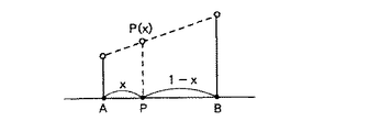
図5は、線形補間処理を示す概念図である。ここで、例えば、注目点Pの両側にある画素AとBに基づき、注目点Pの輝度レベルを演算する。図示のように、注目点Pの輝度レベルは、画素AとBのそれぞれの輝度レベル及び注目点Pの位置に基づいた線形演算で計算される。
【0043】
例えば、図5において、画素AとBの距離を1として、また注目点Pと画素Aの距離をx(0≦x≦1)とする。このため、注目点Pと画素Bとの距離が(1−x)となる。線形補間処理によって求められた注目点Pの輝度レベルは、(1−x)A+xBとなる。
【0044】
キュービック補間処理
キュービック補間処理は、キュービック関数と呼ばれる補間関数に基づき補間係数f(x)を算出し、当該補間係数を用いて、注目点Pの輝度レベルを演算する方式である。なお、キュービック補間処理は、例えば、隣接する4つの画素の画素データに基づき、注目点の輝度レベルを計算する。
【0045】
図6は、キュービック補間処理に用いられている隣接する画素D,B,A,C及び注目点Pの位置関係を示している。図6に示すように、隣接する4つの画素D,B,A,Cは順次配置されている。注目点Pは、画素BとAの間にあり、画素Bとの距離がx(0≦x≦1)となる。これによって、注目点Pと画素Aとの距離が(1−x)、注目点Pと画素Dとの距離が(1+x)、さらに、注目点と画素Cとの距離が(2−x)となる。
【0046】
キュービック補間処理において、変数xに対して補間係数f(x)を次に示す式(3)によって算出される。なお、式(3)において、αは所定の値を取る定数である。
【0047】
【数3】
式(3)は、キュービック式とも呼ばれている。式(3)において、α=−1を例にすると、次式が得られる。
【0049】
【数4】
図7は、式(4)に示す補間係数f(x)の波形を示している。
【0051】
キュービック補間処理において、注目点Pの輝度レベルP(x)は、補間係数f(x)と4つの隣接画素D,B,A,Cのコンボリューションによって求められる。次式は、P(x)を計算する演算式を示している。
【0052】
【数5】
式(5)において、第1項の(1−x)A+xBは、画素AとBの輝度レベルに対する線形補間の結果であり、さらに、第2項の中括弧には、画素AとBの線形補間のほか、画素CとDの線形補間(1−x)C+xDも含まれている。
【0054】
また、式(5)において、その第2項を“0”として、第1項において変数xの値に応じて画素AとBの何れかの輝度レベルを注目点Pの輝度レベルP(x)とすれば、最近傍補間と等価である。これは、次の式によって表される。
【0055】
【数6】
このため、式(5)のみで最近傍補間、線形補間及びキュービック補間(α=−1)の3つの補間処理を実現できる。例えば、この補間処理の切り換えは、図1に示す垂直用画像判別回路20または水平用画像判別回路60から出力されるフラグ信号FLGy またはFLGx に応じて行うことで、処理対象の画像信号にもっとも適している処理方式で補間処理を実現できる。
なお、キュービック関数を用いた補間処理において、上述したα=−1のほか、α=−0.5を用いることもできる。
【0057】
図8〜図10は、上述した補間処理を実現するための補間処理回路の構成例を示す回路図である。なお、図8〜図10に示す回路例は、図1に示す垂直用補間回路10または水平用補間回路50の両方に適用可能である。
【0058】
図8は、補間回路100の構成を示す回路図である。図示のように、補間回路100は、演算回路101,102、選択回路103及び加算回路106、減算回路104、107、109及び乗算回路105、108によって構成されている。
【0059】
演算回路101は、画素データA,B、変数xと(1−x)及びフラグ信号FLG1に基づき、出力信号out1,out2を生成する。出力信号out1は、フラグ信号FLG1によって制御され、画素データAとBに対して、最近傍補間処理または線形処理によって得られた出力である。最近傍補間処理の場合、out1=AまたはB、線形処理の場合に、out1=(1−x)A+xB。出力信号out2は、画素データAとBに対する線形処理によって得られた出力である。即ち、out2=(1−x)A+xB。
【0060】
演算回路102は、画素データC,D、及び変数xと(1−x)に基づき、出力信号out3を生成する。なお、出力信号out3は、画素データCとDに対する線形処理の結果である。即ち、out3=(1−x)C+xD。
【0061】
減算回路107は、変数xに対して、1−xを算出する。
乗算回路108は、変数xの二乗x2 を算出する。
減算回路109は、変数x及び乗算回路108から出力されるx2 に基づき、x−x2 を算出する。
【0062】
減算回路104は、演算回路101から出力される画素AとBの線形処理結果と演算回路102から出力される画素CとDの線形処理結果との差を算出する。
乗算回路105は、減算回路104の出力信号と減算回路104の出力信号との積を算出する。
加算回路106は、乗算回路105の出力信号と演算回路101の出力信号out2とを加算し、加算結果out4を出力する。
即ち、加算回路106の出力信号out4は、式(5)によって与えられるキュービック補間処理の結果である。
【0063】
選択回路103は、フラグ信号FLG2に応じて、演算回路101の出力out1または加算回路106の出力out4の何れかを選択して出力する。上述したように、演算回路101の出力out1は、フラグ信号FLG1によって制御され、画素AとBに対する最近傍補間処理または線形補間処理の結果である。このため、図8に示す補間回路100は、フラグ信号FLG1とFLG2に応じて、入力される隣り合う4つの画素信号A,B,C,Dに対して、最近傍補間、線形補間及びキュービック補間の何れかの処理を行うことができる。
【0064】
図9は、演算回路101の構成例を示し、図10は、演算回路102の構成例を示している。
以下、図9と図10を参照しつつ、演算回路101及び102の構成について説明する。
【0065】
図9に示すように、演算回路101は、乗算回路111、112、加算回路113、選択回路114、115及び比較回路116によって構成されている。
【0066】
乗算回路111は、画素データAと変数1−xとの積を算出し、加算回路113に出力する。
乗算回路112は、画素データBと変数xとの積を算出し、加算回路113に出力する。
加算回路113は、乗算回路111と112の演算結果を加算し、選択回路115に出力する。
即ち、加算回路113の出力は、画素AとBの線形補間の結果である。
【0067】
比較回路116は、変数xと定数0.5とを比較し、比較結果に応じて、選択制御信号Scを生成し、選択回路114に出力する。
選択回路114は、比較回路116からの選択制御信号Scに応じて、画素データAまたはBの何れかを選択し、選択回路115に出力する。
【0068】
比較回路116と選択回路114によって、最近傍補間処理が行われる。ここで、例えば、変数xは、図5に示すように、画素Aと注目点Pとの距離を示しているとする。画素AとBの距離は1であるとすると、変数xが0.5より大きい場合、画素Aが注目点Pにもっとも近く、最近傍補間の結果として画素Aが選択される。逆に、変数xが0.5を超えていない場合、画素Bが注目点Pにもっとも近く、最近傍補間の結果として画素Bが選択される。
【0069】
選択回路115は、フラグ信号FLGに応じて、選択回路114の出力または加算回路113の出力信号の何れかを選択して出力する。フラグ信号FLGに応じて、選択回路114の出力信号が選択されると、出力out1は画素AとBに対する最近傍補間の結果となる。逆に、加算回路113の出力信号が選択されると、出力out1は画素AとBに対する線形補間の結果となる。
一方、出力out2は、加算回路113の出力、即ち、画素AとBに対する線形補間の結果である。
【0070】
次に、演算回路102について説明する。
図10に示すように、演算回路102は、乗算回路121、122及び加算回路123によって構成されている。
【0071】
乗算回路121は、画素データCと変数1−xとの積を算出し、加算回路123に出力する。
乗算回路122は、画素データDと変数xとの積を算出し、加算回路123に出力する。
加算回路123は、乗算回路121と122の演算結果を加算して、その結果を信号out3として出力する。
即ち、加算回路123の出力out3は、画素CとDの線形補間の結果である。
【0072】
以上説明したように、本実施形態の補間回路100は、演算回路101と102の出力信号に基づき、さらに、フラグ信号FLG1とFLG2に応じて、隣接する4つの画素A,B,C,Dに対して、最近傍補間、線形補間またはキュービック補間処理のうち、何れか1つを選択して補間処理を行い、その結果を出力する。
演算回路101によって、入力画像信号に対して最近傍補間または線形補間が施され、補間処理の結果として信号out1が出力される。ここで、最近傍補間または線形補間は、フラグ信号FLG1によって指定される。一方、演算回路101から出力される画素A,Bに対する線形補間の結果及び演算回路102から出力される画素C,Dに対する線形補間の結果に基づき、キュービック補間処理が行われ、その結果として信号out4が出力される。
【0073】
選択回路103によって、フラグ信号FLG2に応じて、演算回路101の出力信号out1とキュービック補間処理の結果out4の何れかが選択される。このため、図8に示す補間回路1つで、最近傍補間、線形補間またはキュービックの何れかを選択して実施することができる。
【0074】
本実施形態の補間処理回路100は、図1に示す画像信号処理装置にある垂直用補間処理回路10及び水平用補間回路50の両方に適用可能である。このため、本実施形態の画像信号処理装置は、入力画像信号の種類を自動的に判別し、判別の結果に基づき、最適な補間処理で画像信号を補間し、画素数の変換を行うことが可能である。
【0075】
【発明の効果】
以上説明したように、本発明の画像信号処理装置、及び、画像信号処理方法によれば、画像信号の種類を自動的に判別することができ、判別の結果に従って画像信号に対して補間処理方式を適宜切り換えて補間処理を行い、画素数変換を行うことができる。
また、本発明によれば、簡単な処理回路によって複数の補間処理を実現することができ、画像信号処理装置の回路構成を簡素化しながら、高画質化の要求に対応することができる利点がある。
【図面の簡単な説明】
【図1】本発明に係る画像信号処理装置の一実施形態を示す構成図である。
【図2】隣接する4画素分の画素データに基づく画像判別処理を示す概念図である。
【図3】隣接する4画素分の画素データに基づく画像判別処理を示す概念図である。
【図4】最近傍補間処理を示す概念図である。
【図5】線形補間処理を示す概念図である。
【図6】キュービック補間処理に用いられる隣接4画素及び注目点の位置関係を示す図である。
【図7】キュービック補間処理に用いられる補間関数の波形を示す波形図である。
【図8】補間処理回路の一構成例を示す回路図である。
【図9】補間処理回路を構成する演算回路の一構成例を示す回路図である。
【図10】補間処理回路を構成する他の演算回路の一構成例を示す回路図である。
【符号の説明】
10…垂直用補間回路、20…垂直用画像判別回路、30−1,30−2,30−3…ラインバッファ、50…水平用補間回路、60…水平用画像判別回路、70−1,70−2,70−3…画素バッファ、100…補間回路、101,102…演算回路。[0001]
BACKGROUND OF THE INVENTION
The present invention relates to an image signal processing apparatus.And image signal processing methodConversion device for converting image resolution by enlarging or reducing image signalAnd image signal processing methodIt is about.
[0002]
[Prior art]
Conventionally, a pixel number conversion circuit used in an image signal processing device is used to display input signals having various display formats in a fixed pixel display device such as an LCD (Liquid Crystal Display) or a PDP (Plasma Display Panel). It was done.
[0003]
In recent years, with the start of BS (Broadcast satellite) digital broadcasting, these images are described above for image signals in which natural images of television broadcasting and text (characters) of data broadcasting and CG (Computer Graphic) are mixed. Display with high image quality is required.
[0004]
In order to meet this demand, various image signal processing methods have been proposed so far for converting the number of pixels. For example, as disclosed in Japanese Patent Application Laid-Open No. 11-055503, which is a patent document, it has been proposed to separately have an interpolation processing circuit for natural images and characters and switch between them appropriately.
According to this publication, the ratio of resolution conversion is an integer ratio M: N (where M and N are integers), and the original image is divided into subdivided regions of M × M pixels, which are included in this. If the type of the color component of the pixel is greater than or equal to a certain threshold value, it is determined as a natural image and the image is processed by a linear interpolation circuit. The document describes that image processing is performed by an adaptive thinning processing circuit corresponding to a correlation coefficient for each subdivided M × M pixel region, and the image is reduced to N × N pixels.
[0005]
Further, as disclosed in Japanese Patent Application Laid-Open No. 2001-189850, which is a patent document, it has been proposed to appropriately switch the interpolation characteristics between a natural image and CG.
According to the publication, in a resolution conversion device in an image processing device for converting the resolution of an image, an image property detection circuit for determining whether a character or a natural image from an image signal in which characters and natural images are mixed, and the character or natural image Interpolating function generating circuit for generating an interpolating function by a cubic convolution method based on the discriminating determination, and a resolution for reducing or enlarging the image signal based on the interpolating function output from the interpolating function generating circuit And a resolution conversion circuit that performs conversion.
[0006]
[Problems to be solved by the invention]
By the way, the above-described conventional image processing method has a problem in image type recognition and interpolation processing optimization. For example, in the method disclosed in Japanese Patent Application Laid-Open No. 11-055503, text including a large amount of color components cannot be recognized as a CG image, and it is necessary to have two systems of nearest neighbor interpolation and linear interpolation. Certainly, linear interpolation cannot meet the demand for higher image quality for the conversion of the natural image portion.
[0007]
Further, in the method disclosed in Japanese Patent Laid-Open No. 2001-189850, the characteristics of the cubic convolution method are appropriately switched. However, since the cubic convolution method is not optimal for the interpolation processing of the CG image, the image quality is improved. There is a disadvantage that it is not possible to respond to the request.
[0008]
The present invention has been made in view of such circumstances, and an object of the present invention is to determine the type of an image signal with high accuracy, and according to a result of the determination, a plurality of interpolations corresponding to each image type are performed by one interpolation processing circuit. An object of the present invention is to provide an image signal processing apparatus that can perform pixel number conversion processing by switching the interpolation method, and can meet the demand for higher image quality while realizing simplification of the circuit configuration.Another object of the present invention is to provide an image signal processing method that can meet the demand for higher image quality.
[0009]
In order to achieve the above object, the image signal processing apparatus according to the present invention determines whether an image signal is a natural image signal or a computer image signal generated by a computer according to an input image signal. And an interpolation processing unit that selects a predetermined interpolation process according to the determination result of the image determination unit, performs the process on the input image signal by the selected interpolation process, and converts the number of pixels.In the image signal processing apparatus, the image discrimination means uses the first, second, third, and fourth pixel data adjacent to the input image signal, and uses the first and second data. Calculating the ratio of the absolute value of the difference between the pixel data and the absolute value of the difference between the third and fourth pixel data and the absolute value of the difference between the second and third pixel data, Based on the comparison result between the calculated ratio and a predetermined threshold value, it is determined whether the input image signal is a natural image signal or a computer image signal.
[0010]
In the present invention, it is preferable that the image discriminating unit performs a predetermined calculation using adjacent pixel data of the input image signal, and the input image signal is natural based on a result of the calculation. Whether the image signal is an image signal or a computer image signal is determined.
[0011]
In the present invention, it is preferable that the interpolation processing unit switches between linear interpolation and cubic interpolation based on the determination result of the image determination unit, and performs interpolation processing on the input image signal. Further, based on the discrimination result of the image discrimination means, the nearest neighbor interpolation and cubic interpolation are switched, and interpolation processing is performed on the input image signal.
[0012]
In the present invention, it is preferable that the interpolation processing unit performs interpolation on the input image signal by switching between linear interpolation, nearest neighbor interpolation, and cubic interpolation based on the determination result of the image determining unit. Process.
[0013]
In the present invention, it is preferable that the image discriminating unit performs the calculation based on luminance data representing the luminance of adjacent pixels in the input image signal, and inputs the input image based on the calculation result. Determine the signal.
[0014]
In the present invention, it is preferable that the interpolation processing unit switches the interpolation processing based on the determination result based on the luminance data, and performs the interpolation processing on the color difference signal of the input image signal.
[0015]
In the present invention, it is preferable that the image determination unit performs the determination in the horizontal direction and the vertical direction with respect to the input image signal. Further, the interpolation processing means performs the interpolation processing in each of the horizontal direction and the vertical direction according to the discrimination results in the horizontal direction and the vertical direction.
[0016]
The image signal processing method according to the present invention includes an image determination step for determining whether the image signal is a natural image signal or a computer image signal generated by a computer according to an input image signal, and the image determination step. An interpolation process step of selecting a predetermined interpolation process according to the determination result, performing the process on the input image signal by the selected interpolation process, and converting the number of pixels. The image discrimination step uses the data of the first, second, third and fourth pixels adjacent to the input image signal to calculate the absolute difference between the first and second pixel data. The ratio of the sum of the value and the absolute value of the difference between the third and fourth pixel data and the absolute value of the difference between the second and third pixel data is calculated, and the calculated ratio and a predetermined value are calculated. Based on the comparison result with the threshold, The input image signal is or natural image of the image signal, determines whether the computer image signal.
[0017]
According to the present invention, the image determination means performs a predetermined calculation based on adjacent pixel data in the input image signal, and determines the type of the input image signal based on the result. Depending on the determination result, the interpolation processing means appropriately switches the interpolation processing method suitable for the type of the input image signal, performs the interpolation processing, and converts the number of pixels. As a result, interpolation processing is performed by an interpolation processing method suitable for the type of image signal, and pixel number conversion is performed. Further, since the interpolation processing means can realize a plurality of different interpolation processes with one circuit, the circuit configuration is simplified.
[0018]
DETAILED DESCRIPTION OF THE INVENTION
FIG. 1 is a block diagram showing an embodiment of an image signal processing apparatus according to the present invention.
As shown in the figure, the image processing apparatus of this embodiment includes a
Hereinafter, the configuration of each partial circuit of the image signal processing apparatus of the present embodiment will be described.
[0019]
The
[0020]
The vertical
[0021]
Line buffers 30-1, 30-2 and 30-3 are connected in series. These line buffers are composed of, for example, a plurality of stages of shift registers connected in series, each storing pixel data for one line, and sequentially storing the stored pixel data from the input stage to the output stage. Forward. For this reason, the pixel data output from the output stage of each line buffer becomes the pixel data one line before the pixel data input to the input stage. That is, in FIG. 1, pixel data C output from the line buffer 30-3.y Is the pixel data A output from the line buffer 30-2.y Pixel data B one line before, and similarly, pixel data B output from the line buffer 30-1y Is the currently input pixel data Dy This is pixel data one line before.
[0022]
Pixel data D interpolated in the vertical direction by the
[0023]
The
[0024]
The horizontal
[0025]
Each of the pixel buffers 70-1, 70-2, and 70-3 is configured by a shift register that holds pixel data for one pixel. These pixel buffers are connected in series to store pixel data for one pixel, and transfer the stored pixel data to the next pixel buffer. For this reason, the pixel data output from each pixel buffer is the pixel data of the previous pixel on the time axis with respect to the input pixel data. For example, pixel data C output from the pixel buffer 70-3x Is the pixel data A output from the pixel buffer 70-2.x Pixel data of the previous pixel, and similarly, pixel data B output from the pixel buffer 70-1x Is the input pixel data Dx Compared to the pixel data of the previous pixel.
[0026]
Next, image discrimination processing and image interpolation processing in the image signal processing apparatus of this embodiment will be described.
[0027]
Image discrimination processing
First, image signal discrimination processing will be described. In the discrimination processing, it is discriminated whether the input image signal is a computer image signal or a natural image signal. The discrimination processing is performed in the vertical and horizontal directions, respectively. The determination in the vertical direction is performed by the vertical
[0028]
Here, it is assumed that pixel data of four adjacent pixels are input in the order of C, A, B, and D on the time axis. The image type is determined by numerical calculation based on the value of pixel data of adjacent pixels (that is, the luminance level of the pixel). Specifically, the vertical or horizontal image discriminating circuit determines whether the “absolute value of the luminance level difference between the pixels A and B”, the “absolute value of the luminance level difference between the pixels B and D”, and the “between the pixels A and C”. Based on the ratio of the absolute value of the luminance level difference to the average value. When this ratio exceeds a predetermined threshold value TH, it is determined as a computer image signal. Conversely, when this ratio does not exceed the threshold value TH, it is determined that the image is a natural image.
The following formulas are used for determining the image type.
[0029]
[Expression 1]
Here, equation (1) can be rewritten as equation (2) below, so that image discrimination processing can be realized without division processing.
[0031]
[Expression 2]
2 and 3 show the concept of image discrimination processing based on pixel data for four adjacent pixels. As shown in the figure, adjacent four pixels D, B, C, A have luminance levels corresponding to the respective pixel data. In the discrimination process, the absolute value | A−B | of the luminance level difference between the pixels A and B, and the absolute value | BD− and | A of the luminance level difference between the pixels D and B and between A and C. −C | is calculated, and an average value K = (| BD | + | A−C |) / 2 of absolute values of luminance level differences between the pixels D and B and between A and C is calculated. The type of the image signal is determined based on the ratio | A−B | / K of the absolute value | A−B | of the luminance level difference between the pixels A and B and the average value K.
[0033]
As described above, here, the average value K of “the absolute value of the luminance level difference between the pixels B and D” and “the absolute value of the luminance level difference between the pixels A and C” is (| B−D Since | + | A−C |) / 2, this average value calculation is not required depending on how the threshold value TH is set. In other words, the image discrimination is performed simply according to the luminance data of the four adjacent pixels D, B, C, and A, and the absolute value | A−B | of the luminance level difference between the pixels A and B and between the pixels D and B. And the sum (| BD | + | AC |) of the absolute value | BD− | of the difference in luminance level between A and C and | AC− |.
[0034]
In the example of the pixel data shown in FIG. 2, the calculated value | A−B | / K is large, for example, larger than a predetermined threshold value TH. Therefore, the image signal is discriminated as a CG image signal, and the flag signal FLG representing the CG image is displayed.y Or FLGx Is output.
On the other hand, in the example of the pixel data shown in FIG. 3, the calculated value | A−B | / K is small, for example, equal to or less than the threshold value TH. Therefore, the image signal is determined to be a natural image signal, and the flag signal FLG representing the natural image is displayed.y Or FLGx Is output.
[0035]
As described above, based on the pixel data of the four adjacent pixels input by the vertical
The vertical
[0036]
Each of the
Hereinafter, the interpolation processing in the image signal processing apparatus of the present embodiment will be described.
[0037]
Image interpolation processing
Image interpolation processing in the image signal processing apparatus of this embodiment is performed in the vertical and horizontal directions, respectively. The vertical interpolation processing is performed by the
[0038]
Since the image interpolation processing in the vertical direction and the horizontal direction is substantially the same, hereinafter, the pixel data of the four adjacent pixels to be input are denoted as A, B, C, and D without particularly distinguishing the vertical or horizontal direction. Interpolation processing will be described.
Here, it is assumed that pixel data of four adjacent pixels are input in the order of C, A, B, and D on the time axis.
[0039]
In the image signal processing apparatus of the present embodiment, the interpolation processing is performed by selecting one of the three processing methods of nearest neighbor interpolation, linear interpolation, or cubic interpolation.
[0040]
Nearest neighbor interpolation
The nearest neighbor interpolation process is an interpolation method in which the luminance level of the pixel closest to the position of the pixel to be obtained (hereinafter referred to as the attention point) is used as the luminance level of the pixel of the attention point.
[0041]
FIG. 4 is a conceptual diagram showing the nearest neighbor interpolation process. As illustrated, the point of interest P is located between adjacent pixels A and B. The pixel closest to the attention point P is the pixel A. For this reason, the luminance level of the point of interest P is set to the luminance level of the pixel A in the nearest neighbor interpolation process.
[0042]
Linear interpolation processing
The linear interpolation process is a method of calculating the luminance level of the attention point by linear calculation using the luminance levels of two or more pixels adjacent to the attention point.
FIG. 5 is a conceptual diagram showing linear interpolation processing. Here, for example, the luminance level of the attention point P is calculated based on the pixels A and B on both sides of the attention point P. As shown in the figure, the luminance level of the attention point P is calculated by linear calculation based on the luminance levels of the pixels A and B and the position of the attention point P.
[0043]
For example, in FIG. 5, the distance between the pixels A and B is 1, and the distance between the point of interest P and the pixel A is x (0 ≦ x ≦ 1). For this reason, the distance between the target point P and the pixel B is (1-x). The luminance level of the target point P obtained by the linear interpolation process is (1−x) A + xB.
[0044]
Cubic interpolation processing
The cubic interpolation process is a method of calculating an interpolation coefficient f (x) based on an interpolation function called a cubic function and calculating the luminance level of the attention point P using the interpolation coefficient. In the cubic interpolation process, for example, the luminance level of the target point is calculated based on the pixel data of four adjacent pixels.
[0045]
FIG. 6 shows the positional relationship between adjacent pixels D, B, A, and C and the point of interest P used in the cubic interpolation process. As shown in FIG. 6, the four adjacent pixels D, B, A, and C are sequentially arranged. The point of interest P is between the pixels B and A, and the distance from the pixel B is x (0 ≦ x ≦ 1). As a result, the distance between the attention point P and the pixel A is (1-x), the distance between the attention point P and the pixel D is (1 + x), and the distance between the attention point and the pixel C is (2-x). Become.
[0046]
In the cubic interpolation process, the interpolation coefficient f (x) is calculated for the variable x by the following equation (3). In Expression (3), α is a constant that takes a predetermined value.
[0047]
[Equation 3]
Expression (3) is also called a cubic expression. In formula (3), when α = −1 is taken as an example, the following formula is obtained.
[0049]
[Expression 4]
FIG. 7 shows the waveform of the interpolation coefficient f (x) shown in Equation (4).
[0051]
In the cubic interpolation process, the luminance level P (x) of the point of interest P is obtained by the convolution of the interpolation coefficient f (x) and the four adjacent pixels D, B, A, and C. The following expression shows an arithmetic expression for calculating P (x).
[0052]
[Equation 5]
In Equation (5), (1-x) A + xB in the first term is the result of linear interpolation with respect to the luminance levels of the pixels A and B, and the curly brackets in the second term indicate the linearity of the pixels A and B. In addition to interpolation, linear interpolation of pixels C and D (1-x) C + xD is also included.
[0054]
In the equation (5), the second term is set to “0”, and the luminance level of the pixel A or B is set to the luminance level P (x) of the attention point P according to the value of the variable x in the first term. This is equivalent to nearest neighbor interpolation. This is represented by the following equation:
[0055]
[Formula 6]
For this reason, three interpolation processes of nearest neighbor interpolation, linear interpolation, and cubic interpolation (α = −1) can be realized only by Expression (5). For example, this interpolation processing is switched by the flag signal FLG output from the vertical
In addition, in the interpolation processing using the cubic function, α = −0.5 can be used in addition to the above α = −1.
[0057]
8 to 10 are circuit diagrams illustrating configuration examples of the interpolation processing circuit for realizing the above-described interpolation processing. The circuit examples shown in FIGS. 8 to 10 are applicable to both the
[0058]
FIG. 8 is a circuit diagram showing a configuration of the
[0059]
The
[0060]
The
[0061]
The
The
The
[0062]
The
The
The
That is, the output signal out4 of the
[0063]
The
[0064]
FIG. 9 shows a configuration example of the
Hereinafter, the configuration of the
[0065]
As shown in FIG. 9, the
[0066]
The
The
The
That is, the output of the
[0067]
The
The
[0068]
The
[0069]
The selection circuit 115 selects and outputs either the output of the
On the other hand, the output out2 is the output of the
[0070]
Next, the
As shown in FIG. 10, the
[0071]
The
The
The
That is, the output out3 of the
[0072]
As described above, the
The
[0073]
The
[0074]
The
[0075]
【The invention's effect】
As described above, the image signal processing apparatus of the present inventionAnd image signal processing methodAccording to the above, the type of the image signal can be automatically discriminated, the interpolation processing method is appropriately switched for the image signal according to the discrimination result, the interpolation processing is performed, and the number of pixels can be converted.
In addition, according to the present invention, a plurality of interpolation processes can be realized by a simple processing circuit, and there is an advantage that it is possible to meet the demand for higher image quality while simplifying the circuit configuration of the image signal processing apparatus. .
[Brief description of the drawings]
FIG. 1 is a configuration diagram showing an embodiment of an image signal processing apparatus according to the present invention.
FIG. 2 is a conceptual diagram showing image discrimination processing based on pixel data for four adjacent pixels.
FIG. 3 is a conceptual diagram showing image discrimination processing based on pixel data for four adjacent pixels.
FIG. 4 is a conceptual diagram showing nearest neighbor interpolation processing;
FIG. 5 is a conceptual diagram illustrating linear interpolation processing.
FIG. 6 is a diagram illustrating a positional relationship between adjacent four pixels and a point of interest used for cubic interpolation processing.
FIG. 7 is a waveform diagram showing a waveform of an interpolation function used for cubic interpolation processing.
FIG. 8 is a circuit diagram showing a configuration example of an interpolation processing circuit.
FIG. 9 is a circuit diagram showing a configuration example of an arithmetic circuit constituting the interpolation processing circuit.
FIG. 10 is a circuit diagram showing a configuration example of another arithmetic circuit constituting the interpolation processing circuit.
[Explanation of symbols]
DESCRIPTION OF
Claims (10)
上記画像判別手段の判別結果に応じて、所定の補間処理を選択し、選択された補間処理で上記入力画像信号に対して処理を行い、画素数変換を行う補間処理手段と
を有する画像信号処理装置であって、
上記画像判別手段は、上記入力される画像信号の隣接する第1、第2、第3及び第4の4つの画素のデータを用いて、上記第1と第2の画素データの差の絶対値と上記第3と第4の画素データの差の絶対値との和と、上記第2と第3の画素データの差の絶対値との比を算出し、当該算出した比と所定のしきい値との比較結果に基づき、上記入力される画像信号が自然画の画像信号か、コンピュータ画像信号かについて判別する
画像信号処理装置。 Image discriminating means for discriminating whether the image signal is an image signal of a natural image or a computer image signal generated by a computer according to an input image signal;
An image signal processing comprising: an interpolation processing unit that selects a predetermined interpolation process according to a determination result of the image determination unit, performs a process on the input image signal by the selected interpolation process, and performs pixel number conversion A device ,
The image discriminating means uses the data of the four adjacent first, second, third and fourth pixels of the input image signal and uses the absolute value of the difference between the first and second pixel data. And the absolute value of the difference between the third and fourth pixel data and the absolute value of the difference between the second and third pixel data are calculated, and the calculated ratio and a predetermined threshold are calculated. Based on the comparison result with the value, it is determined whether the input image signal is a natural image signal or a computer image signal.
Image signal processing device.
請求項1記載の画像信号処理装置。The image discrimination means performs a predetermined calculation using adjacent pixel data of the input image signal, and whether the input image signal is a natural image image signal or a computer image signal based on a result of the calculation. The image signal processing apparatus according to claim 1.
請求項1記載の画像信号処理装置。The image signal processing apparatus according to claim 1, wherein the interpolation processing unit switches between linear interpolation and cubic interpolation based on a determination result of the image determination unit, and performs interpolation processing on the input image signal.
請求項1記載の画像信号処理装置。The image signal processing apparatus according to claim 1, wherein the interpolation processing unit performs interpolation processing on the input image signal by switching between nearest neighbor interpolation and cubic interpolation based on a determination result of the image determining unit.
請求項1記載の画像信号処理装置。The image signal according to claim 1, wherein the interpolation processing means switches between linear interpolation, nearest neighbor interpolation and cubic interpolation based on a determination result of the image determination means, and performs interpolation processing on the input image signal. Processing equipment.
請求項2記載の画像信号処理装置。The image according to claim 2 , wherein the image determination unit performs the calculation based on luminance data representing the luminance of adjacent pixels in the input image signal, and determines the input image signal based on the calculation result. Signal processing device.
請求項6記載の画像信号処理装置。The image signal processing apparatus according to claim 6 , wherein the interpolation processing means switches the interpolation processing based on a determination result based on the luminance data, and performs the interpolation processing on the color difference signal of the input image signal.
請求項1記載の画像信号処理装置。The image signal processing apparatus according to claim 1, wherein the image determination unit performs the determination in the horizontal direction and the vertical direction with respect to the input image signal.
請求項8記載の画像信号処理装置。The image signal processing apparatus according to claim 8, wherein the interpolation processing unit performs the interpolation processing in each of the horizontal direction and the vertical direction in accordance with a determination result in each of the horizontal direction and the vertical direction.
上記画像判別ステップの判別結果に応じて、所定の補間処理を選択し、選択された補間処理で上記入力画像信号に対して処理を行い、画素数変換を行う補間処理ステップと An interpolation processing step of selecting a predetermined interpolation process according to the determination result of the image determination step, performing a process on the input image signal by the selected interpolation process, and converting the number of pixels;
を有する画像信号処理方法であって、 An image signal processing method comprising:
上記画像判別ステップは、上記入力される画像信号の隣接する第1、第2、第3及び第4の4つの画素のデータを用いて、上記第1と第2の画素データの差の絶対値と上記第3と第4の画素データの差の絶対値との和と、上記第2と第3の画素データの差の絶対値との比を算出し、当該算出した比と所定のしきい値との比較結果に基づき、上記入力される画像信号が自然画の画像信号か、コンピュータ画像信号かについて判別する The image determining step uses the data of the four adjacent first, second, third and fourth pixels of the input image signal, and uses the absolute value of the difference between the first and second pixel data. And the absolute value of the difference between the third and fourth pixel data and the absolute value of the difference between the second and third pixel data are calculated, and the calculated ratio and a predetermined threshold are calculated. Based on the comparison result with the value, it is determined whether the input image signal is a natural image signal or a computer image signal.
画像信号処理方法。 Image signal processing method.
Priority Applications (1)
| Application Number | Priority Date | Filing Date | Title |
|---|---|---|---|
| JP2002118278A JP3899994B2 (en) | 2002-04-19 | 2002-04-19 | Image signal processing apparatus and image signal processing method |
Applications Claiming Priority (1)
| Application Number | Priority Date | Filing Date | Title |
|---|---|---|---|
| JP2002118278A JP3899994B2 (en) | 2002-04-19 | 2002-04-19 | Image signal processing apparatus and image signal processing method |
Publications (3)
| Publication Number | Publication Date |
|---|---|
| JP2003319171A JP2003319171A (en) | 2003-11-07 |
| JP2003319171A5 JP2003319171A5 (en) | 2005-09-08 |
| JP3899994B2 true JP3899994B2 (en) | 2007-03-28 |
Family
ID=29535219
Family Applications (1)
| Application Number | Title | Priority Date | Filing Date |
|---|---|---|---|
| JP2002118278A Expired - Fee Related JP3899994B2 (en) | 2002-04-19 | 2002-04-19 | Image signal processing apparatus and image signal processing method |
Country Status (1)
| Country | Link |
|---|---|
| JP (1) | JP3899994B2 (en) |
Cited By (1)
| Publication number | Priority date | Publication date | Assignee | Title |
|---|---|---|---|---|
| EP2028837A2 (en) | 2007-08-21 | 2009-02-25 | NEC Electronics Corporation | Video signal processing device, video signal processing method and display device |
Families Citing this family (4)
| Publication number | Priority date | Publication date | Assignee | Title |
|---|---|---|---|---|
| WO2006075594A1 (en) | 2005-01-11 | 2006-07-20 | Nec Corporation | Template matching method and device, and recording medium where program therefor is recorded |
| JP4742898B2 (en) * | 2006-02-15 | 2011-08-10 | セイコーエプソン株式会社 | Image processing method, image processing program, recording medium, and projector |
| US8594465B2 (en) * | 2007-11-14 | 2013-11-26 | Microsoft Corporation | Adaptive filtering for image transform processes |
| KR101506396B1 (en) | 2013-09-13 | 2015-03-26 | 조선대학교산학협력단 | Image interpolation system and the method |
-
2002
- 2002-04-19 JP JP2002118278A patent/JP3899994B2/en not_active Expired - Fee Related
Cited By (2)
| Publication number | Priority date | Publication date | Assignee | Title |
|---|---|---|---|---|
| EP2028837A2 (en) | 2007-08-21 | 2009-02-25 | NEC Electronics Corporation | Video signal processing device, video signal processing method and display device |
| JP2009049752A (en) * | 2007-08-21 | 2009-03-05 | Nec Electronics Corp | Video signal processing device, video signal processing method and display device |
Also Published As
| Publication number | Publication date |
|---|---|
| JP2003319171A (en) | 2003-11-07 |
Similar Documents
| Publication | Publication Date | Title |
|---|---|---|
| US5991463A (en) | Source data interpolation method and apparatus | |
| JP3013808B2 (en) | Resolution conversion method and display control device using the same | |
| EP0336776A2 (en) | Image magnification | |
| KR20000023569A (en) | Image converter and image conversion method | |
| US6539128B1 (en) | Method and apparatus for interpolation | |
| US6961479B1 (en) | Image processing device, image processing method, image-processing program recorded medium | |
| GB2150797A (en) | Graphic display system | |
| JP3899994B2 (en) | Image signal processing apparatus and image signal processing method | |
| EP0554836B1 (en) | Parabolic waveform generating apparatus | |
| US7532773B2 (en) | Directional interpolation method and device for increasing resolution of an image | |
| US20050078884A1 (en) | Method and apparatus for interpolating a digital image | |
| JP2001189850A (en) | Device and method for converting resolution | |
| JP2003018552A (en) | Scanning line conversion circuit | |
| JPH05207271A (en) | Picture magnification equipment | |
| JP4483255B2 (en) | Liquid crystal display | |
| JPH11203467A (en) | Display and its method | |
| JP2005293361A (en) | Image processing device | |
| JPH09116930A (en) | Method for converting two-dimensional video into three-dimensional video | |
| JPH0738805A (en) | Image enlarging device | |
| JP4197995B2 (en) | Scanning line conversion device, display device, and scanning line conversion method | |
| JP2000115720A (en) | Scanning line interpolation device and scanning line interpolation method | |
| US20040264809A1 (en) | Image processing apparatus, image processing method and image processing system | |
| JP2691582B2 (en) | Pixel density conversion device and method thereof | |
| JPH1117931A (en) | Pixel density converter | |
| JP3444170B2 (en) | Field image interpolation method and field image interpolation device |
Legal Events
| Date | Code | Title | Description |
|---|---|---|---|
| A521 | Request for written amendment filed |
Free format text: JAPANESE INTERMEDIATE CODE: A523 Effective date: 20050316 |
|
| A621 | Written request for application examination |
Free format text: JAPANESE INTERMEDIATE CODE: A621 Effective date: 20050316 |
|
| A977 | Report on retrieval |
Free format text: JAPANESE INTERMEDIATE CODE: A971007 Effective date: 20060908 |
|
| A131 | Notification of reasons for refusal |
Free format text: JAPANESE INTERMEDIATE CODE: A131 Effective date: 20060912 |
|
| A521 | Request for written amendment filed |
Free format text: JAPANESE INTERMEDIATE CODE: A523 Effective date: 20061107 |
|
| TRDD | Decision of grant or rejection written | ||
| A01 | Written decision to grant a patent or to grant a registration (utility model) |
Free format text: JAPANESE INTERMEDIATE CODE: A01 Effective date: 20061205 |
|
| A61 | First payment of annual fees (during grant procedure) |
Free format text: JAPANESE INTERMEDIATE CODE: A61 Effective date: 20061218 |
|
| LAPS | Cancellation because of no payment of annual fees |