JP3882579B2 - Switching amplifier device and protection circuit control method for switching amplifier - Google Patents
Switching amplifier device and protection circuit control method for switching amplifier Download PDFInfo
- Publication number
- JP3882579B2 JP3882579B2 JP2001334947A JP2001334947A JP3882579B2 JP 3882579 B2 JP3882579 B2 JP 3882579B2 JP 2001334947 A JP2001334947 A JP 2001334947A JP 2001334947 A JP2001334947 A JP 2001334947A JP 3882579 B2 JP3882579 B2 JP 3882579B2
- Authority
- JP
- Japan
- Prior art keywords
- switching
- protection
- stopped
- output
- pulse signal
- Prior art date
- Legal status (The legal status is an assumption and is not a legal conclusion. Google has not performed a legal analysis and makes no representation as to the accuracy of the status listed.)
- Expired - Fee Related
Links
Images


Landscapes
- Amplifiers (AREA)
Description
【0001】
【発明の属する技術分野】
本発明は、オーディオ信号をスピーカ駆動用に増幅させるオーディオパワーアンプ装置に関し、特にPWM(Pulse Width Modulation:パルス幅変調)方式などに変調された信号でスイッチング手段を直接駆動して電源増幅を行うスイッチングアンプ装置及びスイッチングアンプの保護回路制御方法に関する。
【0002】
【従来の技術】
従来、オーディオ信号をスピーカ駆動用に増幅させるパワーアンプ装置が各種製品化されている。このオーディオ信号を増幅させるパワーアンプ装置の1つの方式として、入力したデジタルオーディオ信号を変調した信号で、直接電源をスイッチングして、オーディオ信号を増幅させるデジタルパワーアンプ装置と称されるものが開発されている。このデジタルパワーアンプ装置の場合には、例えば入力したデジタルオーディオ信号に基づいて、パルス幅変調(PWM)されたPWM波(以下このPWM波をPWM信号を称する)を生成させ、このPWM信号により安定化された電源を高速でスイッチングさせ、そのスイッチングされた電源をフィルタに供給して、オーディオ信号成分を抽出させる処理を行って、スピーカ駆動信号を得るようにしたものである。
【0003】
PWM信号は、アナログオーディオ信号の波形レベルの大小に応じてパルス幅変調された信号であり、そのPWM信号により、電源をスイッチングするスイッチング手段(パワースイッチ)のオン・オフを制御するものである。
【0004】
そして、スイッチング手段でPWM信号によりスイッチングされた電源を、ローパスフィルタに供給して、高域成分をカットしてオーディオ信号帯域の成分を抽出することで、電源電圧に対応した出力のスピーカ駆動用の増幅信号が得られるものである。
【0005】
【発明が解決しようとする課題】
ところで、このようなデジタルパワーアンプ装置の場合には、スピーカ駆動用の増幅信号を得るスイッチング手段に、何らかの保護回路が必要である。即ち、例えばスピーカ接続端子が、何らかの金属物で短絡された場合や、スイッチング手段に供給する電源に、何らかのノイズが混入したり、静電気が発生した場合には、スイッチング手段に直接これらの影響があるため、保護回路を設けて、これらの異常が発生した際には、スイッチング手段の動作を停止させるように構成する必要がある。
【0006】
ところが、この保護回路が作動すると、入力オーディオ信号のアンプ動作が完全に停止してしまい、いわゆる無音状態となってしまう。従来のデジタルパワーアンプ装置で、この無音状態から復帰させるためには、リセット釦がある場合には、そのリセット釦をユーザが操作する必要があり、またリセット釦がない場合には、パワーアンプ装置の電源を入れ直す操作を行う必要があった。
【0007】
このように、従来のデジタルパワーアンプ装置の場合には、ユーザが手動で操作しないと、保護回路が作動した状態から復帰させることは不可能であり、煩わしい問題があった。
【0008】
また、ユーザから見た場合には、入力したオーディオ信号が無音状態の信号波形であるために、スピーカの出力が無音状態になっているか、或いはパワーアンプ装置の保護回路が作動しているために、スピーカの出力が無音状態になっているのか、迅速に判断することは困難であり、通常はある程度様子を見ないと判らないものであり、ユーザによる迅速な対処は困難であった。
【0009】
また、このように従来のデジタルアンプ装置の保護回路の場合には、一旦作動してしまうと、その復帰に手間がかかるために、なるべく保護回路を作動させなくても良いように、構成する工夫が必要であった。具体的には、例えばアンプ装置の内部に大型のシールドケースを設置したり、ノイズ対策用のコンデンサやダイオードなどを回路に追加する等して、外部からのノイズの影響を軽減させるようにしてあり、このような対処のために、デジタルアンプ装置の製造コストを上昇させてしまう問題があった。
【0010】
本発明はかかる状況に鑑みてなされたものであり、スイッチング素子を使用したアンプ装置の保護回路の復帰が、自動的に行えることを目的とする。
【0011】
【課題を解決するための手段】
本発明は、入力したオーディオ信号波形に基づいてスピーカ駆動用のパルス信号を得るスイッチング手段と、スイッチング手段の入力又は出力の異常を検出した場合にスイッチング手段のスイッチング動作を停止させて保護動作を行う保護手段と、スイッチング手段が出力する上記パルス信号を平滑化するフィルタ手段と、フィルタ手段の出力電圧を所定の閾値と比較しパルス信号が停止していることを判定する判定手段と、判定手段によって上記パルス信号が停止状態と見なしたとき、スイッチング手段のスイッチング動作が停止していることを検出する検出手段と、検出手段がスイッチング手段の動作が停止していることを検出したとき保護手段による保護動作をリセットさせてスイッチング手段によるパルス信号の出力を再開させる制御手段とを備えたものである。
【0012】
本発明によると、保護手段が作動したとき、自動的に制御手段が保護動作をリセットさせる動作が実行されて、スイッチング手段によるスピーカ駆動用のパルス信号の出力が再開されるようになる。
【0013】
【発明の実施の形態】
以下、添付図面を参照して、本発明の一実施の形態について説明する。
【0014】
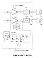
図1は、本例のデジタルパワーアンプ装置10の全体構成を示す図である。図1では説明を簡単にするために、1チャンネルの処理構成だけを示してあるが、実際には2チャンネルなど複数チャンネルのオーディオ信号を処理できるように構成される。
【0015】
本例のデジタルパワーアンプ装置10は、外部のオーディオ信号源(図示せず)から端子11に得られるデジタルオーディオ信号を、ゲインコントロール部12に供給して、ゲイン調整を行い、そのゲイン調整されたデジタルオーディオ信号を、デジタルシグマ変換器13で、1ビット方式のデジタルオーディオデータに変換し、変換された1ビット方式のデジタルオーディオデータを、信号処理部14に供給し、スイッチング素子を駆動するためのPWM信号を生成させる。
【0016】
信号処理部14で生成されたPWM信号は、スイッチング増幅部15に供給し、電源回路18から供給される安定化された直流電源を、PWM信号に基づいてオン・オフ制御し、電源にオーディオ信号成分を重畳させる。本例のスイッチング増幅部15は、集積回路で構成されており、スイッチング増幅部15が備えるスイッチング素子としては例えば電界効果トランジスタを使用する。スイッチング増幅部15でスイッチングされた信号は、ローパスフィルタ(LPF)16に供給して、スイッチングにより発生した高周波成分を除去してオーディオ信号成分だけを抽出し、その抽出されたオーディオ信号成分を、スピーカ駆動信号としてスピーカ接続端子17に接続されたスピーカ装置1に供給し、このスピーカ装置1から所定の音量でオーディオ(音声)を出力させる。
【0017】
なお、スイッチング素子は、後述する保護回路15aが作動しているとき以外は、常時スイッチング動作を行うようにしてあり、例えば無音状態のときでも、一定の周波数のパルス信号が出力されるようにしてある。ローパスフィルタ16でのスイッチング周波数に相当する高周波成分の除去を行うことで、オーディオ信号成分だけが、スピーカ装置側に供給されるようになる。例えば、スイッチング素子で約250KHzのパルス信号を生成させるようにしてあり、ローパスフィルタ16でこの約250KHzの信号成分を除去して、いわゆる可聴帯域(例えば数十kHz程度まで)のオーディオ信号成分が、スピーカ接続端子17から出力されるようにしてある。
【0018】
また、このデジタルパワーアンプ装置10は、各種操作キーや音量調整用のボリュームつまみ等で構成される操作部19を備えて、この操作部19の操作状況をCPU20が判断して、CPU20が音量調整などの各種制御を行うようにしてある。
【0019】
ここで、本例のスイッチング増幅部15は、保護回路15aを内蔵させてある。保護回路15aは、電源回路18からスイッチング増幅部15に入力する電源の異常、入力するPWM信号の異常、スイッチング素子でスイッチングされた出力の異常(短絡など)を検出して、その異常検出時には、全てのチャンネルのスイッチング素子でのスイッチング動作を停止させて、このスイッチング増幅部15からの出力、即ち、スピーカ接続端子17からのスピーカ駆動信号の出力を停止させる構成としてある。
【0020】
この保護回路15aは、CPU20から供給されるリセット信号により、保護動作が実行されたときのその保護動作のリセットが行われるようにしてある。
【0021】
CPU20は、この保護回路15aが作動して、スイッチング素子でのスイッチング動作が停止しているか否か判断するために、スイッチング増幅部15の出力を判断する構成としてある。即ち、スイッチング増幅部15内の何れか1チャンネルのスイッチング素子の出力を、ローパスフィルタ21で平滑化して、そのローパスフィルタ21の出力を、CPU20のアナログ/デジタル変換器22に供給して、電圧値に対応したデータに変換し、そのアナログ/デジタル変換器22で変換されたデータを、CPU20内で判断し、その判断したデータに基づいて、保護回路15aにリセット信号を出力するようにしてある。ここでのリセット信号の出力とは、リセット信号として、一時的にローレベル信号“L”を保護回路15aに供給することであり、リセット時以外はCPU20から保護回路15aにハイレベル信号“H”を供給するようにしてある。リセット信号を出力する判定処理については後述する。
【0022】
ローパスフィルタ21は、スピーカ接続端子16側に設けられたローパスフィルタ16とは特性の異なるフィルタである。即ち、スイッチング増幅部15内のスイッチング素子がスイッチング動作を行っているときと、スイッチング動作を行っていないときで、異なる電圧値となるようなフィルタとしてある。具体的には、例えばカットオフ周波数が3Hz程度のローパスフィルタを使用して、PWM信号で変調されたパルス信号の直流化を行うようにしてある。
【0023】
図2は、本例のデジタルアンプ装置10の保護動作に関係した構成を、より詳細に示した図である。図2では、スイッチング増幅部15として、2チャンネルの信号を処理する構成として示してあり、左チャンネル用のスイッチング素子15Lと、右チャンネル用のスイッチング素子15Rを備える。それぞれのチャンネル用のスイッチング素子15L,15Rによりスイッチングされた出力信号を、各チャンネル毎のローパスフィルタ16L,16Rを介して、スピーカ接続端子17L,17Rに供給する。ローパスフィルタ16L,16Rは、スイッチングにより生じた高周波成分を除去するフィルタである。左右のチャンネルのスピーカ接続端子17L,17Rには、各チャンネル用のスピーカ装置1L,1Rが接続される。
【0024】
ここで本例においては、一方のチャンネル(図2では右チャンネル)のスイッチング素子15Rの出力の一方の極に得られる信号を、ローパスフィルタ21を介してCPU20内のアナログ/デジタル変換器22に供給するように構成してある。ローパスフィルタ21としては、既に説明したように、カットオフ周波数が3Hz程度のフィルタである。ここでは、例えば、抵抗器R1とダイオードD1とを直列に接続し、ダイオードD1と変換器22の入力との間に、抵抗器R2の一端と、コンデンサC1の一端と、ダイオードD2のカソードとを接続し、抵抗器R2の他端と、コンデンサC1の他端と、ダイオードD2のアノードとを、それぞれ接地側に接続させて、ローパスフィルタとして構成させてある。
【0025】
このような構成のローパスフィルタ21を通過させることで、ここではスイッチング素子が正常にスイッチング動作を行っているときには、ローパスフィルタ21の出力として、0.8V以上の電圧となるようにしてあり、スイッチング素子によるスイッチング動作が停止しているときには、0.8V未満のほぼ0Vに近い電圧となるようにしてある。即ち、スイッチング素子が正常にスイッチング動作を行っているときには、例えば図3Aに示すように、約250kHzのパルス信号がスイッチング素子から出力される。このパルス信号波形は、オーディオ信号波形により変化するが、無音状態のオーディオ信号の場合でも、パルス信号の基本的な周波数は同じである。本例では、このパルス信号をローパスフィルタ21を通過させることで、0.8V以上の電圧となるようにしてある。これに対して、スイッチング素子がスイッチング動作を停止しているときには、図3Bに示すように、0Vなどの一定電圧となる。
【0026】
そして、CPU20では、アナログ/デジタル変換器22の出力が0.8V以上のデータか否か判断するようにしてある。
【0027】
次に、CPU20での、アナログ/デジタル変換器22の出力データに基づいた制御処理を、図4のフローチャートを参照して説明する。
【0028】
CPU20は、メインルーチン(ステップS10)から、保護回路の動作状態の判定処理がスタートするサブルーチンに移ると(ステップS11)、アナログ/デジタル変換器22の出力データを読み込んで、ローパスフィルタ21の出力電圧値を判定し記憶する(ステップS12)。そして、このとき判定した電圧値が、0.8V未満か否か判断する(ステップS13)。0.8V未満でない場合(即ち0.8V以上である場合)には、このサブルーチンを終了し(ステップS16)、ステップS10のメインルーチンに戻る。その後、約10msの周期で、ステップS11の保護回路の動作状態を判定するサブルーチンに移る。
【0029】
そして、ステップS13の判断で、電圧値が0.8V未満であると判断したときには、前回のサブルーチンで判定して記憶した電圧値が0.8V未満であったか否か判断する(ステップS14)。ここで、前回判定した電圧値が0.8V以上であるときには、ステップS16に移ってこのサブルーチンを終了し、ステップS10のメインルーチンに戻る。そして、ステップS14の判断で、0.8V未満であると判断したときには、ステップS15に移り、リセット信号を10ms間、ローレベル信号“L”とし、その後ハイレベル信号“H”に戻す処理を行い、その後ステップS16に移って、このサブルーチンを終了する。
【0030】
ステップS15での10ms間のローレベル信号“L”が、リセット信号として保護回路15aに供給されることで、保護回路15aはリセット動作が行われて、保護回路15aの作動でスイッチング動作が停止しているスイッチング素子15L,15Rのスイッチング動作が復帰するようになり、接続されたスピーカ装置からのオーディオの出力が再開される。
【0031】
このようにCPU20が制御動作を行うことで、ローパスフィルタ21の出力電圧が、0.8V未満となったことが約10ms間隔で2回連続して検出されたとき、スイッチング増幅部15内の保護回路15aが作動して、スイッチング動作が停止していると判断して、保護回路15aにリセット信号が供給されて、保護回路15aによる保護動作がリセットされて、スイッチング増幅部15でのスイッチング動作が再開される。従って、電源ノイズなどの一時的な要因で保護回路が作動したとき、その作動から約10ms後に自動的に復帰するようになる。従って、保護回路作動時のスピーカ装置からのオーディオの出力としては、一時的にわずかの時間だけ途切れるだけであり、ユーザがリセット釦を操作したり、アンプ装置の電源を入れ直すような操作が必要なくなる。
【0032】
また、このように保護回路が作動した際に、わずかな時間の経過後に自動的に復帰するようにしたことで、このわずかな時間の一時的な出力停止が許容できるアンプ装置である場合には、シールド板やコンデンサなどによるノイズ対策に、それほどコストをかける必要がなくなり、アンプ装置の製作コストを低減させることが可能になる。
【0033】
さらに本例の場合には、図4のフローチャートのステップS13,S14に示すように、10ms間隔で2回連続してスイッチング出力の電圧を判断するようにしたので、一時的な誤検出による誤動作の影響を回避でき、確実に保護回路の作動を検出できるようになる。
【0034】
なお、図4のフローチャートに示した例では、2回連続してスイッチング出力が停止状態であるとき、保護回路に対してリセット信号を供給するようにしたが、そのリセット信号の供給後に、さらに連続して保護回路が作動するようなときには、リセット信号の供給を行わないようにしても良い。図5のフローチャートは、この場合の処理例を示した図である。
【0035】
図5のフローチャートの動作について説明すると、CPU20は、メインルーチン(ステップS10)から、保護回路の動作状態の判定処理がスタートするサブルーチンに移ると(ステップS11)、アナログ/デジタル変換器22の出力データを読み込んで、ローパスフィルタ21の出力電圧値を判定し記憶する(ステップS12)。そして、このとき判定した電圧値が、0.8V未満か否か判断する(ステップS13)。0.8V未満でない場合(即ち0.8V以上である場合)には、このサブルーチンを終了し(ステップS16)、ステップS10のメインルーチンに戻る。その後、約10msの周期で、ステップS11の保護回路の動作状態を判定するサブルーチンに移る。
【0036】
そして、ステップS13の判断で、電圧値が0.8V未満であると判断したときには、前回のサブルーチンで判定して記憶した電圧値が0.8V未満であったか否か判断する(ステップS14)。ここで、前回判定した電圧値が0.8V以上であるときには、ステップS16に移ってこのサブルーチンを終了し、ステップS10のメインルーチンに戻る。ここまでは、図4のフローチャートに示した処理と同じである。
【0037】
そして、ステップS14の判断で、0.8V未満であると判断したときには、ステップS17に移って、10回以上連続して、判定した電圧値が0.8V未満であったか否か判断する。この判断で、判定した電圧値が0.8V未満であることが10回以上連続している場合には、ステップS16に移ってこのサブルーチンを終了し、ステップS10のメインルーチンに戻り、リセット動作は行わない。そして、ステップS17で、判定した電圧値が連続して0.8V未満であった回数が10回未満であると判断したときには、ステップS15に移り、リセット信号を10ms間、ローレベル信号“L”とし、その後ハイレベル信号“H”に戻す処理を行い、その後ステップS16に移って、このサブルーチンを終了する。
【0038】
この図5のフローチャートに示すように処理することで、リセット動作を行って保護回路による保護動作をリセットしても、直後に再度保護動作が行われるようになった場合には、保護動作のリセットが実行されなくなり、保護回路が作動して、スイッチング動作が停止したままになる。
【0039】
このようにリセットしても直ぐに保護動作が行われる場合には、保護回路が作動する原因が除去されてないことが想定され、その場合には、保護回路が作動する原因(例えばスピーカ接続端子の短絡など)を除去してから、ユーザがリセット釦を押したり、或いは電源を入れ直すことで、従来と同様に、保護回路の作動を復帰させることが可能になる。
【0040】
なお、上述した実施の形態では、1ビット方式のデジタルオーディオデータに基づいてパルス幅変調されたPWM信号を生成させて、パワースイッチのスイッチングを制御するようにしたが、PDM(Pulse Duration Modulation )方式などのその他のパルス変調された信号でスイッチングを制御して、増幅された信号を得る各種方式のスイッチングアンプ装置にも、本発明が適用できるものである。
【0041】
また、上述した実施の形態では、入力したオーディオ信号に基づいて、接続されたスピーカ装置を駆動させる単体のアンプ装置として構成したが、再生装置などのオーディオ信号源やスピーカ装置などが一体化されたオーディオ機器のアンプ部にも本発明が適用できることは勿論である。
【0042】
また、上述した実施の形態では、スイッチング増幅部とスピーカ接続端子との間に、スイッチングにより発生した高周波成分を除去するローパスフィルタ(図1でのローパスフィルタ16に相当)を設ける構成としたが、接続されるスピーカ装置側に同様のローパスフィルタが接続されている場合、或いはスピーカ装置の特性上から、高域の除去が不要の場合には、出力用のローパスフィルタを省略しても良い。
【0043】
【発明の効果】
本発明によると、保護手段が作動しても自動的に保護動作をリセットさせる動作が実行される。従って、一時的なノイズなどの入力で保護手段が作動した場合には、保護手段が作動しているわずかな時間だけ一時的に無音状態になるだけで、ユーザが復帰動作を行うことなく自動的に復帰し、電源ノイズなどにより保護手段が作動して無音状態が継続するのを効果的に防止できるようになる。
【0044】
この場合、検出手段として、スイッチング手段が出力するパルス信号を平滑化するフィルタ手段と、このフィルタ手段の出力電圧を判定する判定手段とで構成し、判定手段がパルス信号無しの状態の電圧を検出したとき、スイッチング動作が停止していることを検出するようにしたことで、スイッチング動作が停止していることを簡単に検出できるようになる。
【0045】
また、スイッチング手段が出力するスピーカ駆動用のパルス信号は、検出手段が備えるフィルタ手段とは別のフィルタ手段で高周波成分を除去して、スピーカに供給するようにしたことで、それぞれのフィルタ手段の特性を最適に設定でき、スイッチング動作の検出とスピーカ供給用の出力とを良好に行える。
【0046】
また、所定の回数連続してスイッチング動作が停止していることを検出手段が検出したとき、制御手段は保護手段による保護動作をリセットさせることで、保護動作が行われる状態が継続していることを確実に検出した上でリセットさせる動作が実行されるようになる。
【0047】
さらに、このように所定の回数連続してスイッチング動作が停止していることを検出したときにリセットさせるようにした場合に、リセットの直後に、さらにスイッチング動作が停止していることを検出手段が検出したときにはリセットを行わないようにしたことで、保護手段を作動させる要因が継続している場合には、リセットさせる動作が実行されなくなり、保護機能が有効に機能するようになる。
【図面の簡単な説明】
【図1】本発明の一実施の形態による全体構成の例を示すブロック図である。
【図2】本発明の一実施の形態による保護動作に関係した部分の構成の例を示す構成図である。
【図3】スイッチング増幅部の出力波形例を示す波形図である。
【図4】本発明の一実施の形態による復帰動作の例を示すフローチャートである。
【図5】本発明の他の実施の形態による復帰動作の例を示すフローチャートである。
【符号の説明】
1,1L,1R…スピーカ装置、10…デジタルパワーアンプ装置、11…入力端子、12…ゲインコントロール部、13…デジタルシグマ変換部、14…信号処理部、15…スイッチング増幅部、15L,15R…スイッチング素子、16,16L,16R…ローパスフィルタ、17,17L,17R…出力端子、18…電源回路、19…操作部、20…中央制御ユニット(CPU)、21…ローパスフィルタ、22…アナログ/デジタル変換器[0001]
BACKGROUND OF THE INVENTION
The present invention relates to an audio power amplifier device that amplifies an audio signal for driving a speaker, and in particular, switching that directly powers a switching means with a signal modulated by a PWM (Pulse Width Modulation) method and performs power supply amplification. The present invention relates to an amplifier device and a switching amplifier protection circuit control method.
[0002]
[Prior art]
Conventionally, various types of power amplifier devices that amplify audio signals for driving speakers have been commercialized. As a method of a power amplifier device for amplifying the audio signal, a so-called digital power amplifier device for amplifying the audio signal by directly switching the power source with a signal obtained by modulating the input digital audio signal has been developed. ing. In the case of this digital power amplifier device, for example, based on the input digital audio signal, a pulse wave modulated (PWM) PWM wave (hereinafter referred to as a PWM signal) is generated and stabilized by this PWM signal. The switched power supply is switched at high speed, the switched power supply is supplied to a filter, and an audio signal component is extracted to obtain a speaker drive signal.
[0003]
The PWM signal is a signal that is pulse-width modulated in accordance with the waveform level of the analog audio signal. The PWM signal controls on / off of switching means (power switch) that switches the power source.
[0004]
Then, the power source switched by the PWM signal by the switching means is supplied to the low-pass filter, and the high frequency component is cut and the audio signal band component is extracted, so that the output of the speaker corresponding to the power source voltage is used for driving the speaker. An amplified signal is obtained.
[0005]
[Problems to be solved by the invention]
By the way, in the case of such a digital power amplifier device, some kind of protection circuit is necessary for the switching means for obtaining the amplified signal for driving the speaker. That is, for example, when the speaker connection terminal is short-circuited with some metal object, or when some noise is mixed in the power supply supplied to the switching means or static electricity is generated, these effects are directly applied to the switching means. Therefore, it is necessary to provide a protection circuit so that the operation of the switching means is stopped when these abnormalities occur.
[0006]
However, when this protection circuit is activated, the amplifier operation of the input audio signal is completely stopped, resulting in a so-called silent state. In the conventional digital power amplifier device, in order to recover from the silent state, if there is a reset button, the user needs to operate the reset button. If there is no reset button, the power amplifier device It was necessary to perform the operation to turn on the power again.
[0007]
As described above, in the case of the conventional digital power amplifier device, unless the user manually operates, it is impossible to return from the state in which the protection circuit is activated, and there is a troublesome problem.
[0008]
In addition, when viewed from the user, the input audio signal is a silent signal waveform, so the speaker output is silent, or the power amplifier device protection circuit is activated. In addition, it is difficult to quickly determine whether the output of the speaker is in a silent state, and it is usually impossible to determine the appearance of the speaker to some extent, and it is difficult for the user to quickly deal with it.
[0009]
In addition, in the case of the protection circuit of the conventional digital amplifier device as described above, once it is activated, it takes time to restore it, so that the protection circuit is not required to be activated as much as possible. Was necessary. Specifically, for example, a large shield case is installed inside the amplifier device, or a noise countermeasure capacitor or diode is added to the circuit to reduce the influence of external noise. For this reason, there has been a problem of increasing the manufacturing cost of the digital amplifier device.
[0010]
The present invention has been made in view of such a situation, and an object of the present invention is to automatically restore the protection circuit of an amplifier device using a switching element.
[0011]
[Means for Solving the Problems]
The present invention provides a switching means that obtains a pulse signal for driving a speaker based on an input audio signal waveform, and performs a protection operation by stopping the switching operation of the switching means when an abnormality in the input or output of the switching means is detected. A protection means , a filter means for smoothing the pulse signal output from the switching means, a determination means for comparing the output voltage of the filter means with a predetermined threshold value to determine that the pulse signal is stopped, and a determination means. When the pulse signal is considered to be in a stopped state, the detecting means for detecting that the switching operation of the switching means is stopped, and the protection means when the detecting means detects that the operation of the switching means is stopped Reset the protection operation and resume the output of the pulse signal by the switching means. It is obtained by a means.
[0012]
According to the present invention, when the protection means is activated, the control means automatically performs an operation of resetting the protection operation, and the output of the speaker driving pulse signal by the switching means is resumed.
[0013]
DETAILED DESCRIPTION OF THE INVENTION
Hereinafter, an embodiment of the present invention will be described with reference to the accompanying drawings.
[0014]
FIG. 1 is a diagram illustrating an overall configuration of a digital
[0015]
The digital
[0016]
The PWM signal generated by the
[0017]
Note that the switching element always performs a switching operation except when a
[0018]
The digital
[0019]
Here, the switching
[0020]
The
[0021]
The
[0022]
The low-
[0023]
FIG. 2 is a diagram showing in more detail the configuration related to the protection operation of the
[0024]
Here, in this example, a signal obtained at one pole of the output of the
[0025]
By passing through the low-
[0026]
The
[0027]
Next, control processing based on the output data of the analog /
[0028]
When the
[0029]
When it is determined in step S13 that the voltage value is less than 0.8V, it is determined whether or not the voltage value determined and stored in the previous subroutine is less than 0.8V (step S14). Here, when the previously determined voltage value is 0.8 V or more, the process proceeds to step S16 to end the subroutine, and returns to the main routine of step S10. If it is determined in step S14 that the voltage is less than 0.8 V, the process proceeds to step S15, where the reset signal is set to the low level signal “L” for 10 ms, and then returned to the high level signal “H”. Thereafter, the process proceeds to step S16, and this subroutine is terminated.
[0030]
Since the low level signal “L” for 10 ms in step S15 is supplied as a reset signal to the
[0031]
When the
[0032]
In addition, when the protection circuit is activated in this way, it is automatically restored after a lapse of a short time, so that the amplifier device can tolerate a temporary output stop for a short time. In addition, it is not necessary to spend so much cost on noise countermeasures such as a shield plate and a capacitor, and the manufacturing cost of the amplifier device can be reduced.
[0033]
Further, in the case of this example, as shown in steps S13 and S14 in the flowchart of FIG. 4, the voltage of the switching output is judged twice continuously at an interval of 10 ms. The influence can be avoided and the operation of the protection circuit can be reliably detected.
[0034]
In the example shown in the flowchart of FIG. 4, the reset signal is supplied to the protection circuit when the switching output is in a stopped state twice consecutively. However, after the reset signal is supplied, the reset signal is further continuously supplied. When the protection circuit is activated, the reset signal may not be supplied. The flowchart of FIG. 5 is a diagram illustrating a processing example in this case.
[0035]
The operation of the flowchart of FIG. 5 will be described. When the
[0036]
When it is determined in step S13 that the voltage value is less than 0.8V, it is determined whether or not the voltage value determined and stored in the previous subroutine is less than 0.8V (step S14). Here, when the previously determined voltage value is 0.8 V or more, the process proceeds to step S16 to end the subroutine, and returns to the main routine of step S10. Up to this point, the processing is the same as that shown in the flowchart of FIG.
[0037]
If it is determined in step S14 that the voltage is less than 0.8V, the process proceeds to step S17, and it is determined whether or not the determined voltage value is less than 0.8V continuously for 10 times or more. If it is determined in this determination that the determined voltage value is less than 0.8 V for 10 times or more, the process proceeds to step S16 to end this subroutine, and returns to the main routine in step S10. Not performed. If it is determined in step S17 that the determined voltage value is continuously less than 0.8 V is less than 10, the process proceeds to step S15, and the reset signal is set to the low level signal “L” for 10 ms. Then, the process of returning to the high level signal “H” is performed, and then the process proceeds to step S16 to end this subroutine.
[0038]
If the reset operation is performed and the protection operation by the protection circuit is reset by performing the processing as shown in the flowchart of FIG. 5, if the protection operation is performed again immediately after that, the protection operation is reset. Is not executed, the protection circuit is activated, and the switching operation remains stopped.
[0039]
If the protection operation is performed immediately after resetting in this way, it is assumed that the cause of the activation of the protection circuit has not been removed. In this case, the cause of the activation of the protection circuit (for example, the speaker connection terminal When the user depresses the reset button or turns the power on again after removing the short circuit or the like, the operation of the protection circuit can be restored as in the conventional case.
[0040]
In the above-described embodiment, a PWM signal that is pulse-width modulated based on 1-bit digital audio data is generated to control the switching of the power switch. However, the PDM (Pulse Duration Modulation) method is used. The present invention can also be applied to various types of switching amplifier devices in which switching is controlled by other pulse-modulated signals such as those to obtain an amplified signal.
[0041]
Further, in the above-described embodiment, although configured as a single amplifier device that drives a connected speaker device based on an input audio signal, an audio signal source such as a playback device, a speaker device, and the like are integrated. Of course, the present invention can also be applied to an amplifier section of an audio device.
[0042]
In the above-described embodiment, the low-pass filter (corresponding to the low-
[0043]
【The invention's effect】
According to the present invention, the operation of automatically resetting the protection operation is executed even if the protection means is activated. Therefore, when the protection means is activated by an input of temporary noise, etc., the user can be silent automatically for a short period of time during which the protection means is activated. Thus, it is possible to effectively prevent the protection means from operating due to power noise or the like and continuing the silent state.
[0044]
In this case, the detection means comprises a filter means for smoothing the pulse signal output from the switching means and a determination means for determining the output voltage of the filter means, and the determination means detects a voltage without a pulse signal. In this case, it is possible to easily detect that the switching operation is stopped by detecting that the switching operation is stopped.
[0045]
The pulse signal for driving the speaker output from the switching means is removed from the high frequency component by a filter means different from the filter means provided in the detection means and is supplied to the speaker. The characteristics can be set optimally, and the switching operation can be detected and the output for supplying the speaker can be satisfactorily performed.
[0046]
In addition, when the detection means detects that the switching operation has been stopped for a predetermined number of times, the control means resets the protection operation by the protection means, so that the state in which the protection operation is performed continues. The operation of resetting after reliably detecting is performed.
[0047]
Further, when resetting is performed when it is detected that the switching operation has been stopped for a predetermined number of times in this way, the detection means detects that the switching operation has further stopped immediately after the reset. Since the reset is not performed at the time of detection, when the factor for operating the protection means continues, the reset operation is not executed, and the protection function functions effectively.
[Brief description of the drawings]
FIG. 1 is a block diagram illustrating an example of an overall configuration according to an embodiment of the present invention.
FIG. 2 is a configuration diagram showing an example of a configuration of a portion related to a protection operation according to an embodiment of the present invention.
FIG. 3 is a waveform diagram illustrating an example of an output waveform of a switching amplifier.
FIG. 4 is a flowchart showing an example of a return operation according to an embodiment of the present invention.
FIG. 5 is a flowchart showing an example of a return operation according to another embodiment of the present invention.
[Explanation of symbols]
DESCRIPTION OF
Claims (5)
ス信号を得るスイッチング手段と、
上記スイッチング手段の入力又は出力の異常を検出した場合に、上記スイッチ
ング手段のスイッチング動作を停止させて保護動作を行う保護手段と、
上記スイッチング手段が出力するパルス信号を平滑化するフィルタ手段と、
上記フィルタ手段の出力電圧を所定の閾値と比較し上記パルス信号が停止していることを判定する判定手段と、
上記判定手段によって上記パルス信号が停止状態と見なしたとき、上記スイッチング手段のスイッチング動作が停止していることを検出する検出手段と、
上記検出手段が上記スイッチング手段の動作が停止していることを検出したとき、上記保護手段による保護動作をリセットさせて、上記スイッチング手段によるパルス信号の出力を再開させる制御手段とを備えた
スイッチングアンプ装置。Switching means for obtaining a speaker driving pulse signal based on the input audio signal waveform;
Protection means for stopping the switching operation of the switching means and performing a protection operation when an abnormality in the input or output of the switching means is detected;
Filter means for smoothing the pulse signal output by the switching means;
Determining means for comparing the output voltage of the filter means with a predetermined threshold value to determine that the pulse signal is stopped;
Detecting means for detecting that the switching operation of the switching means is stopped when the pulse signal is regarded as being stopped by the determining means;
When the detecting means detects that the operation of the switching means is stopped, by resetting the protection operation by the protection means, switching amplifier and control means for resuming the output of the pulse signal by said switching means apparatus.
上記スイッチング手段が出力するスピーカ駆動用のパルス信号は、上記検出手
段が備えるフィルタ手段とは別のフィルタ手段で高周波成分を除去して、スピー
カに供給する
ことを特徴とするスイッチングアンプ装置。The switching amplifier device according to claim 1 ,
The speaker driving pulse signal output from the switching unit is supplied to the speaker after removing a high frequency component by a filter unit different from the filter unit included in the detection unit.
A switching amplifier device characterized by that .
所定の回数連続してスイッチング動作が停止していることを上記検出手段が検
出したとき、上記制御手段は上記保護手段による保護動作をリセットさせない
ことを特徴とするスイッチングアンプ装置。The switching amplifier device according to claim 1,
When the detection means detects that the switching operation has been stopped for a predetermined number of times, the control means does not reset the protection operation by the protection means
A switching amplifier device characterized by that .
上記制御手段は、上記リセットの直後に、さらに上記スイッチング動作が停止
していることを上記検出手段が検出したときには、上記制御手段はリセットを行
わない
ことを特徴とするスイッチングアンプ装置。The switching amplifier device according to claim 1 ,
The control means does not reset when the detection means detects that the switching operation is further stopped immediately after the reset.
A switching amplifier device characterized by that .
上記スイッチングステップの入力又は出力の異常を検出した場合に、上記スイッチングステップのスイッチング動作を停止させて保護動作を行う保護ステップと、
上記スイッチングステップが出力するパルス信号を平滑化するフィルタステップと、
上記フィルタステップの出力電圧を所定の閾値と比較し上記パルス信号が停止していることを判定する判定ステップと、
上記判定ステップによって上記パルス信号が停止状態と見なしたとき、上記スイッチング手段のスイッチング動作が停止していることを検出する検出ステップと、
上記検出ステップが上記スイッチングステップが停止していることを検出したとき、上記保護ステップによる保護動作をリセットさせて、上記スイッチングステップによるパルス信号の出力を再開させる
ことを特徴とするスイッチングアンプの保護回路制御方法。A switching step for obtaining a pulse signal for driving the speaker based on the input audio signal waveform;
A protection step for stopping the switching operation of the switching step and performing a protection operation when an abnormality in the input or output of the switching step is detected;
A filter step for smoothing the pulse signal output by the switching step;
A determination step of comparing the output voltage of the filter step with a predetermined threshold value to determine that the pulse signal is stopped;
A detection step for detecting that the switching operation of the switching means is stopped when the pulse signal is regarded as being stopped by the determination step;
When the detecting step detects that the switching step is stopped, by resetting the protection operation by the protection step, to resume the output of the pulse signal by said switching step
A switching amplifier protection circuit control method.
Priority Applications (1)
| Application Number | Priority Date | Filing Date | Title |
|---|---|---|---|
| JP2001334947A JP3882579B2 (en) | 2001-10-31 | 2001-10-31 | Switching amplifier device and protection circuit control method for switching amplifier |
Applications Claiming Priority (1)
| Application Number | Priority Date | Filing Date | Title |
|---|---|---|---|
| JP2001334947A JP3882579B2 (en) | 2001-10-31 | 2001-10-31 | Switching amplifier device and protection circuit control method for switching amplifier |
Publications (3)
| Publication Number | Publication Date |
|---|---|
| JP2003142956A JP2003142956A (en) | 2003-05-16 |
| JP2003142956A5 JP2003142956A5 (en) | 2005-06-23 |
| JP3882579B2 true JP3882579B2 (en) | 2007-02-21 |
Family
ID=19149998
Family Applications (1)
| Application Number | Title | Priority Date | Filing Date |
|---|---|---|---|
| JP2001334947A Expired - Fee Related JP3882579B2 (en) | 2001-10-31 | 2001-10-31 | Switching amplifier device and protection circuit control method for switching amplifier |
Country Status (1)
| Country | Link |
|---|---|
| JP (1) | JP3882579B2 (en) |
Families Citing this family (4)
| Publication number | Priority date | Publication date | Assignee | Title |
|---|---|---|---|---|
| JP4873856B2 (en) * | 2004-12-22 | 2012-02-08 | 株式会社平和 | Game machine |
| JP4801357B2 (en) * | 2005-02-21 | 2011-10-26 | ローム株式会社 | Signal amplification circuit and electronic device using the same |
| CN100533938C (en) * | 2008-04-21 | 2009-08-26 | 南京航空航天大学 | Six-bridge arm five-path output electromagnetic bearing switch power amplifier control method |
| WO2013046354A1 (en) * | 2011-09-28 | 2013-04-04 | 三菱電機株式会社 | Vehicle proximity notification device |
-
2001
- 2001-10-31 JP JP2001334947A patent/JP3882579B2/en not_active Expired - Fee Related
Also Published As
| Publication number | Publication date |
|---|---|
| JP2003142956A (en) | 2003-05-16 |
Similar Documents
| Publication | Publication Date | Title |
|---|---|---|
| US11431310B2 (en) | Tracking and correcting gain of open-loop driver in a multi-path processing system | |
| US8416017B2 (en) | Circuit and method for reducing noise in class D amplifiers | |
| US20090160547A1 (en) | Method and system for transitioning between operation states in an output system | |
| KR100618408B1 (en) | Pulse width modulator for use in a digital amplifier, method for reducing pop noise in a digital amplifier and digital amplifier | |
| JPS61212905A (en) | Apparatus and method for controlling and preventing noise | |
| US11284192B2 (en) | Speaker driver and operation method thereof | |
| KR20070043002A (en) | Dual mode audio amplifier | |
| US20060109049A1 (en) | Low noise audio amplifier | |
| US10044323B1 (en) | Reducing audio artifacts in an amplifier with configurable final output stage | |
| EP1006650B1 (en) | BTL amplifier apparatus | |
| US8686789B2 (en) | Transient signal suppression for a class-D audio amplifier arrangement | |
| JP3882579B2 (en) | Switching amplifier device and protection circuit control method for switching amplifier | |
| KR20190037302A (en) | Configurable control loop topology for pulse width modulated amplifiers | |
| JP2006340152A (en) | Digital amplification method and digital amplification circuit | |
| US7269264B2 (en) | Method for reproducing audio signal from at least two different sources | |
| JP4281004B2 (en) | PWM power amplifier and control method thereof | |
| US10020778B1 (en) | Reducing audio artifacts in an amplifier with configurable final output stage | |
| JP3638442B2 (en) | Volume circuit | |
| JPH1127058A (en) | Pulse width modulation audio amplifier | |
| JP2012209770A (en) | Fixed sound generator and switching amplifier | |
| JP2004208216A (en) | Pulse width modulator/amplifier | |
| JPS6375591A (en) | Power source controller by timer of audio device | |
| JPH0744996A (en) | Noise reduction circuit | |
| JPH0543529Y2 (en) | ||
| JP2006094148A (en) | Digital amplifier |
Legal Events
| Date | Code | Title | Description |
|---|---|---|---|
| A521 | Written amendment |
Free format text: JAPANESE INTERMEDIATE CODE: A523 Effective date: 20041007 |
|
| A621 | Written request for application examination |
Free format text: JAPANESE INTERMEDIATE CODE: A621 Effective date: 20041007 |
|
| A977 | Report on retrieval |
Free format text: JAPANESE INTERMEDIATE CODE: A971007 Effective date: 20060720 |
|
| A131 | Notification of reasons for refusal |
Free format text: JAPANESE INTERMEDIATE CODE: A131 Effective date: 20060801 |
|
| A521 | Written amendment |
Free format text: JAPANESE INTERMEDIATE CODE: A523 Effective date: 20061002 |
|
| TRDD | Decision of grant or rejection written | ||
| A01 | Written decision to grant a patent or to grant a registration (utility model) |
Free format text: JAPANESE INTERMEDIATE CODE: A01 Effective date: 20061024 |
|
| A61 | First payment of annual fees (during grant procedure) |
Free format text: JAPANESE INTERMEDIATE CODE: A61 Effective date: 20061106 |
|
| LAPS | Cancellation because of no payment of annual fees |