JP3854833B2 - Imaging apparatus, signal processing method thereof, program, and storage medium - Google Patents
Imaging apparatus, signal processing method thereof, program, and storage medium Download PDFInfo
- Publication number
- JP3854833B2 JP3854833B2 JP2001273014A JP2001273014A JP3854833B2 JP 3854833 B2 JP3854833 B2 JP 3854833B2 JP 2001273014 A JP2001273014 A JP 2001273014A JP 2001273014 A JP2001273014 A JP 2001273014A JP 3854833 B2 JP3854833 B2 JP 3854833B2
- Authority
- JP
- Japan
- Prior art keywords
- reading
- image data
- field
- white balance
- image
- Prior art date
- Legal status (The legal status is an assumption and is not a legal conclusion. Google has not performed a legal analysis and makes no representation as to the accuracy of the status listed.)
- Expired - Fee Related
Links
Images


Classifications
-
- H—ELECTRICITY
- H04—ELECTRIC COMMUNICATION TECHNIQUE
- H04N—PICTORIAL COMMUNICATION, e.g. TELEVISION
- H04N23/00—Cameras or camera modules comprising electronic image sensors; Control thereof
- H04N23/80—Camera processing pipelines; Components thereof
- H04N23/84—Camera processing pipelines; Components thereof for processing colour signals
- H04N23/88—Camera processing pipelines; Components thereof for processing colour signals for colour balance, e.g. white-balance circuits or colour temperature control
Description
【0001】
【発明の属する技術分野】
本発明は、ホワイトバランス演算を行う撮像装置に関するものである。
【0002】
【従来の技術】
従来、固体メモリ素子を有するメモリカードを記録媒体として、CCD等の撮像素子で撮像した静止画像を撮像するデジタルカメラ等の撮像装置が市販されている。
【0003】
これらの撮像装置では、撮像素子からの出力データを一旦バッファメモリへ取り込んで撮影処理を行い、さらに画像処理及び圧縮処理を施して再度バッファメモリへ格納する現像圧縮処理を行った後、取り外し可能なカード上の記録媒体へ書き込む処理が行われるのが一般的である。
【0004】
このような撮像装置の撮影処理におけるホワイトバランス制御に関しては、従来、以下の手順で実行されていた。まず撮像素子からメモリに取り込まれた信号処理されていない未処理の生データ(以降RAW画像データと呼ぶ)を読み出し、読み出された画像データ中の白と認識される画像データを所定のアルゴリズムにより抽出してホワイトバランス(WB)係数を決定し(以降この処理をWB演算と呼ぶ)、演算の結果得られるWB係数を色信号に乗じることで白データの補正を行う方法が用いられている。
【0005】
そして、1行おきにインターレース走査で読み出されるフレーム読み出し方式の撮像素子を用いた場合、2フィールドで1画面分のRAW画像データが生成されるが、撮像素子の色フィルタ配列が図7に示すようなベイヤー配列の場合、1フィールド読み出しただけではR信号とG信号しかえられず、全ての色情報は得られない。ホワイトバランスの演算では少なくともR,B信号が必要であり、WB演算のアルゴリズムでは、RGBの全ての信号を用いて生成される輝度信号を必要とするケースもある。つまり、1行おきにインターレース走査で読み出されるフレーム読み出し方式の撮像素子を用いた場合、従来は2フィールド、つまり1フレーム(画面)分のRAWデータがメモリに書き込まれるのを待ってから、WB演算を開始していた。そのため、WBの演算に時間を考慮しなければならず、例えば、静止画の連続撮影の際には、撮像コマ間の時間を短縮化するための妨げの原因となっていた。
【0006】
【発明が解決しようとする課題】
本願発明は、上述した問題を解決したものであり、ホワイトバランスの処理の短縮化を目的とするものである。
【0007】
【課題を解決するための手段】
上述した目的を達成するために、本願発明によれば、第1、第2、第3の異なる色成分を含む色フィルタを備え、被写体像を撮像して1画面分の画像データを取得する撮像手段を有する撮像装置において、
前記撮像手段から、1フィールド期間ごとに1ラインおきにインターレース走査して、前記第1と前記第2の色成分を含む第1フィールドと、前記第2と前記第3の色成分を含む第2フィールドを1フレーム期間で順次読み出して出力する読み出し手段と、
前記読み出し手段から出力された画像データ中の複数の色成分信号に基づいてホワイトバランス係数を演算するホワイトバランス演算手段と、
前記ホワイトバランス演算手段は、前記読み出し手段により、前記第1フィールドで前記第1と前記第2の色成分を読み出し、前記第2フィールドで前記第2と前記第3の色成分を読み出すことによって、前記第1フィールドの読み出し終了後、前記第2フィールド目の画像データの読み出し動作と並行してホワイトバランス係数を演算することを特徴とする撮像装置を提供する。
【0008】
また、第1、第2、第3の異なる色成分を含む色フィルタを備え、被写体像を撮像して1画面分の画像データを取得する撮像手段を有する撮像装置の信号処理方法であって、
前記撮像手段から、1フィールド期間ごとに1ラインおきにインターレース走査して、前記第1フィールドで前記第1と前記第2の色成分を読み出し、前記第2フィールドで前記第2と前記第3の色成分を1フレーム期間で順次読み出して出力することによって、前記第1フィールドの読み出し終了後、第2フィールド目の画像データの読み出し動作と並行して前記撮像手段から出力された画像データ中の複数の色成分信号に基づいてホワイトバランス係数を演算することを特徴とする撮像装置の信号処理方法を提供する。
【0009】
【発明の実施の形態】
以下、添付の図面に沿って本発明の実施の形態を説明する。
【0010】
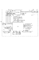
図1は、本発明の実施の一形態である、インターレース走査の1行読み出しを行うことにより全画面の画像出力を1フレーム期間で読み出すフレーム読み出し方式の撮像素子を使用して静止画を撮影する撮像装置の構成を示す図である。
【0011】
図1において、撮像装置本体100は以下の構成を有する。撮影レンズ10は、ズームレンズおよびフォーカスレンズを含む。光学ファインダ11は被写体像を確認するためのものである。シャッター12は絞り機能を兼用している。撮像素子14はCCDなどによって構成され、図7に示すような原色モザイクフィルタを介して光学像を電気信号に変換する。前置処理回路15は内部に撮像素子14の出力ノイズ除去のためのCDS(相関2重サンプリング)回路やAGC(自動利得制御)回路を含む。A/D変換器16は前置処理回路15から出力されるアナログ信号をデジタル信号に変換する。
【0012】
タイミング発生回路(TG)18は撮像素子14、 A/D変換器16にクロック信号や制御信号を供給し、タイミングは信号処理IC22により制御される。
【0013】
信号処理IC22はCPU50からの指示により、A/D変換器16からのデータ或いはDRAM30からのデータに対して所定の画素補間処理や色変換処理、拡大・縮小、画像データ形式変換を行う。また、DMAコントローラ、D/A変換器、画像データを圧縮伸長する圧縮・伸長回路を内蔵している。さらに信号処理IC22は、撮像した画像データを用いて所定の演算処理を行い、得られた演算結果をDRAM30に保存する。CPU50はこの演算結果に基づいてTTL方式のAWB(オートホワイトバランス)処理、AF(オートフォーカス)処理、AE(自動露出)処理、EF(ストロボプリ発光)処理を行っている。
【0014】
画像表示部TFT LCD等から成り、DRAM30に書き込まれた表示用の画像データは信号処理IC22内部のD/A変換器(不図示)を介して画像表示部28により表示される。すなわち、記録した画像を再生するだけでなく画像表示部28を用いて撮像した画像データを逐次表示すれば、電子ファインダ機能を実現することが可能である。画像表示部28は画像の他、各種情報・モード設定状況の表示にも使用される。また、画像表示部28は、CPU50の指示により任意に表示をON/OFFすることが可能であり、表示をOFFにした場合には装置本体100の電力消費を大幅に低減することが出来る。また、画像表示部28の表示部分をカメラ本体側に向けることで表示部分を保護しつつ格納することが可能であり、この場合は検知SW98により、格納状態を検知して画像表示部28の表示動作を停止することが出来る。
【0015】
DRAM30は撮影した非圧縮データの一時格納、AF/AE/AWB/EF演算結果の保持、画像表示部28への表示用画像の保持、圧縮画像データの保持等に使用されるメモリであり、所定枚数の静止画像や所定時間の動画像を格納するのに十分な記憶量を備えている。
【0016】
ズーム制御回路は撮影レンズ10および光学ファインダ11のズーミングを制御する。
【0017】
コネクタ46はアクセサリーシューとも呼ばれ、外部ストロボ装置400との電気接点や機械的な固定手段を備えている。外部ストロボ装置400は、アクセサリーシューと接続するためのコネクタ402,外部ストロボ404を有する。また、内蔵ストロボ48はTTL調光機能を有している。
【0018】
CPU50はデジタルカメラ装置100全体を制御ものであり、信号処理IC22によってDRAM30に格納されたAF/AE/AWB/EFの演算結果に基づき、AF/AE/AWB/EF制御を行う他、信号処理IC22に対するデータフロー制御、各種キースキャン動作、ズーム制御、周辺モジュールとの通信等を行っている。メモリ52はCPU50の動作用の変数等を記憶する。
【0019】
通知部54はCPU50でのプログラムの実行に応じて、文字、画像、音声等を用いて動作状態やメッセージ等を表示する液晶表示装置、スピーカー等の表示部であり、装置本体100の操作部近辺の視認し易い位置に単数或いは複数個所設置され、例えばLCDやLED、発音素子等の組み合わせにより構成されている。
【0020】
通知部54の表示内容としては、シングルショット/連写撮影表示、セルフタイマー表示、圧縮率表示、記録画素数表示、記録枚数表示、残撮影可能枚数表示、シャッタースピード表示、絞り値表示、露出補正表示、ストロボ表示、赤目緩和表示、マクロ撮影表示、ブザー設定表示、時計用電池残量表示、電池残量表示、エラー表示、複数桁の数字による情報表示、記録媒体200の着脱状態表示、通信I/F動作表示、日付・時刻表示、等がある。
【0021】
フラッシュメモリ56は電気的に消去・記録可能であり、CPU50を動作させるために必要なプログラムやカメラ固有の調整データ等があらかじめ書き込まれている。
【0022】
以下主な操作部材の具体的な説明を行う。
【0023】
モードダイヤルスイッチ60は2段構造となっており、下段には電源オフ(OFF)、撮影モード、再生モードの3つの状態が切換可能である。また、上段には撮影時、目的・シーンに合わせてユーザが設定する各種撮影モードが割り当てられており、全自動撮影モード(AUTO)、プログラム撮影モード、シャッター速度優先撮影モード、絞り優先撮影モード、マニュアル撮影モード、パンフォーカスモード、ポートレートモード、風景モード、夜景モード、色効果モード、スティッチアシストモード、動画撮影モードの各モードを切り替え設定することが出来る。
【0024】
シャッタースイッチ64は2段階のスイッチSW1,SW2で構成されている。シャッターボタン64を半押しすることでSW1がONとなり、AF(オートフォーカス)処理、AE(自動露出)処理、AWB(オートホワイトバランス)処理)処理等の動作開始を指示する。さらにシャッターボタンを全押しすることによりSW2がONとなり、撮像素子14から読み出した信号をA/D変換器16、信号処理IC30を介してDRAM30に画像データを書き込む。次に信号処理IC30はCPU50からの指示に従って、DRAM30から画像データを読み出し、色補正、画素補間、色変換等の画像処理を行った後、圧縮処理を行い、記録媒体200に画像データを書き込む。
【0025】
ストロボ切替SW68は、撮影時のストロボの発光モードを強制発光・非発光・自動発光の各モードに切り替える。
【0026】
ドライブモード切替ボタン78はボタンを押す度に、サイクリックに単写/連写/セルフタイマーの切り替えを行う。
【0027】
電源制御部80は、電池検出回路、DC−DCコンバータ、通電するブロックを切り替えるスイッチ回路等により構成されており、電池の装着の有無、電池の種類、電池残量の検出を行い、検出結果及びCPU50の指示に基づいてDC−DCコンバータを制御し、必要な電圧を必要な期間、記録媒体を含む各部へ供給し、必要に応じて通知部54、画像表示部28に電池残量表示を行う。
【0028】
82及び84はコネクタであり、86はアルカリ電池やリチウム電池等の一次電池やNiCd電池やNiMH電池、Li電池等の二次電池、ACアダプター等からなる電源供給部である。
【0029】
記録媒体200はメモリカードやハードディスク等からなり、半導体メモリや磁気ディスク等から構成される記録部202、デジタルカメラ装置100とのインタフェース204、デジタルカメラ装置100と接続を行うコネクタ206を備えている。コネクタ92はメモリカードやハードディスク等の記録媒体と接続を行う。
【0030】
検知部98は、画像表示部28の表示部分を撮像装置100に向けて格納した格納状態にあるかどうかを検知することが出来る検知SW、電池蓋が開けられたことを検出する電池蓋開閉検出SW、外部ストロボ404の装着状態検出SW等が含まれる。
【0031】
図2及び図3は本実施の形態における撮像装置100の主ルーチンのフローチャートである。図2及び図3を用いて、撮像装置100の主動作を説明する。
【0032】
CPU50は、モードダイアル60の設定位置を判断し、モードダイアル60が電源OFFに設定されていたならば(S203)、表示部28の表示を終了状態に変更し、絞り兼用シャッター12を閉じて撮像部を保護する。そして、フラグや制御変数等を含む必要なパラメータや設定値、設定モードをメモリ52に記録し、電源制御部80により画像表示部28を含むデジタルカメラ装置100各部の不要な電源を遮断する等の所定の終了処理を行った後(S205)、S203に戻る。
【0033】
モードダイアル60が撮影モードに設定されていたならば(S203)、S206に進む。モードダイアル60がその他のモードに設定されていたならば(S203)、CPU50は選択されたモードに応じた処理を実行し(S204)、処理を終えたならばS203に戻る。
【0034】
CPU50は、電源制御部80により電池等により構成される電源86の残容量や動作状況が撮像装置100の動作に問題があるか否かを判断し(S206)、問題があるならば画像表示部28あるいは通知部54を用いて画像や音声により所定の警告表示を行った後に(S208)、S203に戻る。
【0035】
電力供給部86に問題が無いならば(S206)、CPU50は記録媒体200の動作状態が撮像装置100の動作、特に記録媒体に対する画像データの記録再生動作に問題があるか否かを判断し(S207)、問題があるならば画像表示部28あるいは表示部54を用いて画像や音声により所定の警告表示を行った後に(S208)、S203に戻る。
【0036】
記録媒体200の動作状態に問題が無いならば(S207)、S208に進む。
【0037】
その後、スルー画像(静止画を撮影する前後にファインダ機能として表示させるための撮像素子14によって撮像された動画像)を画像表示部28に表示するための撮影準備の初期化を行い(S208)、準備が完了したらスルー画像を画像表示部28に表示開始する(S209)。
【0038】
次にスルー画像表示状態における静止画撮影時のカメラ動作について図3を参照しながら説明する。
【0039】
モードダイアル60が変更されていたら(S301)、S203に戻りダイアル状態をチェックする。変更されていなければ、次に検知部98ドライブモード切替ボタン78、ストロボ切替SW68の少なくともいずれかに変化がないかをチェックし(S304)、もし変更があれば変更された個所に応じた処理を行う(S305)。
【0040】
シャッタースイッチSW1が押されていないならば(S306)、スルー画表示を継続して行うための処理を行う。さらに信号処理IC22が撮像素子14から得られた信号に対して所定の測光演算を行いその演算結果をDRAM30に格納する。CPU50はこの演算結果を元にスルー画像に対するAE・AWB処理を行う(S307)。その後S301に戻る。
【0041】
S306においてシャッタースイッチSW1が押されたならば、CPU50は、DRAM30に格納されているフォーカス情報および測光用情報に基づいて、測距演算を行い撮影レンズ10の焦点を被写体に合わせ、測光演算を行い撮影モード毎のプログラム線図に従って得られた絞り値に絞り兼用シャッター12を制御する(S308)。
【0042】
次にSW2の状態をチェックする(S309)。まだSW2が押されていなければ、その後再度シャッターSW1の状態を見て(S310)シャッタースイッチSW1が離されたらS307へ戻る。SW1が押されていた場合には再びSW2の状態を監視しつづける(S309)。
【0043】
S309において、SW2が押された場合は、現状の測光結果及び撮影モード毎のプログラム線図を参照して、撮影時のシャッター速度・撮像出力ゲイン・ストロボ発光等の設定を最終的に決定する(S311)。さらに画像表示部28に表示していたスルー画像表示を停止し、撮影シーケンスに移行する(S312)。
【0044】
まず一連の撮影動作を行う撮影処理を実行する(S313)。撮影処理後DRAM30には、撮像素子14からA/D変換器16を通して読み出された信号処理前の未処理の画像データ(以降このデータをRAW画像データと呼ぶこととする)が保存されている。信号処理IC22はCPU50からの指示に従い、このRAWデータをDRAM30から読み出し、まず撮影処理で得られたWB係数をもとに色補正(ホワイトバランス補正)を行う(S314)。
【0045】
そして、JPEGなどの所定の現像・圧縮処理を行い処理後の画像データをDRAM30内に保存する(S315)。そして、処理後の画像データを表示用画像に変換し再びDRAM30に格納する。この表示用画像データを信号処理IC22が所定のレートで読み出し、D/A変換後、画像表示部28に出力することにより、撮影された静止画の確認画像表示を行う(S316)。S315でDRAM30に保存された圧縮画像データを記録媒体200へ書き込み(S317)、S307へ戻る。
【0046】
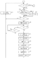
図4は、ステップS313の撮影処理の詳細を示す動作処理フローチャートである。
【0047】
CPU50は、撮像素子14から出力されたRAW画像データをDRAM30に一時保存するためのDRAM書込み設定を行う(S401)。DRAM30への書き込みは、インターレース読み出しに従い、1ラインおきに書き込まれるようにDMAコントローラに対して書き込みアドレスの設定を行う。
【0048】
そして、タイミング発生回路18に対して電子シャッター停止指令を出して露光を開始させるとともに、絞り兼用シャッター12のシャッター閉じタイミングを、予め決定したシャッター秒時に従ってCPU内蔵タイマにセットする(S402)。CPU内蔵タイマは指定された時間が経過したところで絞り兼用シャッター12を全閉するパルスを出力するように設計されている。
【0049】
次にシャッター12が閉じるのを待って(S403)、S401で設定したDRAM領域のうち、まずS401で行った書き込み設定に応じて第1フィールドに対する書き込み開始命令を発行するとともに撮像素子14から第1フィールドの画像データ(奇数列)を読み出すようタイミング発生器18に対して指示を出す(S404)。さらに、DRAM30に対する第1フィールドのRAW画像データ書き込み動作が完了すると(S405)、第2フィールドに対する書き込み開始命令を発行するとともに撮像素子14から第2フィールドの画像データ(偶数列)を読み出すようタイミング発生器18に対して指示を出す(S406)。
【0050】
DRAM30に対する第1フィールドのRAW画像データ書き込み動作が完了すると(S405)、第2フィールドに対する書き込み開始命令を発行するとともに撮像素子14から第2フィールドの画像データを読み出すようタイミング発生器18に対して指示を出す(S406)。
【0051】
第2フィールドのXライン目のDRAM30に対する書き込み動作が終了したかどうかを判断し(S407)、Xライン目の書き込み動作が終了した場合、信号処理IC22はDRAM30に第2フィールドの途中まで書き込まれている画像データを第1フィールドの1ライン目、第2フィールドの1ライン目、第1フィールドの2ライン目…といったように、撮像素子14からの第2フィールドの画像データの読み出し動作が完了する前に図7の上から順に画像データを読み出してWB演算をスタートさせる(S407)。次にDRAM30に対する第2フィールドのRAWデータ書き込み動作の完了を待って(S409)、完了したら次の撮影が迅速に行えるようにメカシャッターの開き動作、電子シャッター動作の再開等などの撮影後処理を行う(S410)。さらにWB(ホワイトバランス)係数の演算が終了したかどうかを判断し(S411)、完了した場合1枚の静止画の撮影処理を終了する。
【0052】
ここで、S407におけるXライン目の決定方法について説明する。このXライン目の決定方法については、第2フィールドへのDRAM書き込み完了がWB演算時のDRAM読み出し完了よりも先に終わることを保証する必要がある。
【0053】
図5は、X=2とした場合の、DRAMに読み出される画素とWB係数の演算開始の様子を示したタイミングチャートである。
【0054】
図5において、時刻t0のタイミングでタイミング発生器18から第1フィールドの読み出しパルスが出力されると、図7に示すような撮像素子14の受光部に蓄積された画像データのうちRおよびGの色フィルタを持つ画素が1ラインおきに撮像素子14、前置処理回路15、A/D変換器16、信号処理IC22を通してDRAMへ出力される。図5では時刻t1の時点で全画素のうち半分(奇数ライン)が完全にDRAM30に格納される。
【0055】
次に時刻t2でタイミング発生器18から第2フィールド読み出しパルスが出力されると、受光部に蓄積された画像データのうち残りの半分、すなわちGおよびBの色フィルタに対応する偶数ラインの画像データが同様にDRAM30へ出力される。そして、時刻t3の時点で第2フィールドの2ライン目までBおよびGの画像データが読み出された時点で、WB係数演算用のメモリ読み出しが開始され、時刻t4で全画素がDRAM30に格納される。そして時刻t5でWB係数演算におけるメモリ読み出しが終了する。
【0056】
図6はX=2とした場合の、時刻t3におけるDRAM30内のRAW画像データの配置をイメージ化したものである。図6に示すように、DRAM30内ではインターレース状に1ラインおきにデータを書き込む設定となっている。
【0057】
図6において、1ライン〜4ライン目まで全色がそろった状態となっているが、この部分についてはWB係数の演算が可能である。6ライン以降の偶数ラインについては、時刻t3の時点では行われていないため、データが存在しない状態となっている。
【0058】
本実施形態のインターレース読み出し型撮像素子14において、
(撮像素子の画素データの読み出し速度)×2>(WB係数演算時のDRAM30からの画素データの読み出し速度)
の関係が成り立っていれば、第2フィールド画像データのDRAM30への書き込み動作を、WB係数演算のDRAM読み出しが追い越すことはないため、Xは余裕を見て数ライン程度に設定しておけばよいことになる。
【0059】
上式の関係が成り立っていない場合は、図5において、第2フィールド画像データのDRAM30への取り込みに要する時間をTw、WB演算時のメモリ読み出しに要する時間をTrとした時、
t3−t2>Tw−Tr
が成立するようにt2を決定すれば、第2フィールド画像データのDRAM30への書き込み動作に対して、WB係数演算のためのDRAM読み出しが追い越すことはなくなる。
【0060】
以上説明したように、本実施形態の撮像装置100においては、撮像素子14から読み出した全ての画像データがDRAM30に格納される前に、ホワイトバランス係数演算用のメモリ読み出し動作を開始させている。このため、撮影後、ホワイトバランス処理動作が完了するまでの時間が大幅に短縮できる。本実施形態では、画像表示部28において、静止画像を確認するための画像表示をホワイトバランス処理動作後に行っているが、この確認画像の表示がなされるまでの時間が短時間で済むため撮影後のストレスから解放されるという、大きなメリットがある。
【0061】
上記実施形態においては1枚静止画像撮影におけるホワイトバランス処理を示したが、本実施の形態のホワイトバランス処理動作を静止画の連続撮影に適用することもできる。この場合、画像撮影のコマ間の時間を短縮させることができる。例えば、静止画の連続撮影を行う際、ホワイトバランスの係数の演算処理を1枚目の静止画の撮影だけ行い、2枚目以降の撮影画像に対しては1枚目のものと同じものを使って処理される構成が考えられている。本実施の形態により、2枚目以降の連写間隔に対して1枚目と2枚目の間の連写間隔が長くなることが緩和され、1枚目からほぼ等間隔で静止画の連続撮影を行うことができるようになった。
【0062】
なお、本実施の形態において,ホワイトバランス係数の演算処理速度(DRAM30からの画像データの読み出し速度)が、撮像素子14からの画像データの読み出し速度よりも十分に早いときには、撮像素子14からの2フィールド目に読み出された画像データをDRAM30に格納せずにホワイトバランス係数の演算を行うこともできる。この場合、撮像素子14からの2フィールド目に読み出される画像データに連動してDRAM30に格納されている第1フィールド目の画像データを順次読み出すことによって達成されることになる。
【0063】
また、図3のS307のスルー画像表示におけるホワイトバランスの処理は、画像表示部28に表示されるに耐えることができる画像処理を行うだけでよいので、図4に示すような処理は必要ない。
【0064】
本発明は、一例として、前述した実施形態の機能を実現するソフトウェアのプログラムコードを、インターネットなどのネットワークを介して画像信号処理装置に供給し、撮像装置のコンピュータ(またはCPUやMPU)が記憶媒体に格納されたプログラムコードを読み出し実行することによって達成できる。
【0065】
この場合、記憶媒体から読み出されたプログラムコード自体が前述した実施形態のCPU50の機能を実現することになり、そのプログラムコードを記憶した記憶媒体は本発明を構成することになる。
【0066】
プログラムコードを供給するための記憶媒体としては、例えば、フロッピーディスク、ハードディスク、光ディスク、光磁気ディスク、CD−ROM、CD−R、磁気テープ、不揮発性のメモリカード、ROMなどを用いることができる。
【0067】
また、コンピュータが読み出したプログラムコードを実行することにより、前述した実施形態の機能が実現されるだけでなく、そのプログラムコードの指示に基づき、コンピュータ上で稼動しているOS(オペレーティングシステム)などが実際の処理の一部または全部を行い、その処理によって前述した実施形態の機能が実現される場合も含まれる。
【0068】
さらに、記憶媒体から読み出されたプログラムコードが、コンピュータに挿入された機能拡張ボードやコンピュータに接続された機能拡張ユニットに備わるメモリに書き込まれた後、そのプログラムコードの指示にもとづき、その機能拡張ボードや機能拡張ユニットに備わるCPUなどが実際の処理の一部または全部を行い、その処理によって前述した実施形態の機能が実現される。
【0069】
本発明を上記記憶媒体に適用する場合、その記憶媒体には、先に説明したフローチャートに対応するプログラムコードを格納することになるが、簡単に説明すると、本発明の撮像装置に不可欠なモジュールを、記憶媒体に格納することになる。
【0070】
【発明の効果】
以上説明したように、本願発明によれば、被写体像を撮像して1フィールド期間ごとに1ラインおきの画素をインターレース走査して第1フィールド、第2フィールドの画像を順次出力することによって1画面分の画像データを取得し、撮影後ホワイトバランス演算を撮像素子からの画像データの読み出し動作と一部を並行して実行するようにしたので、例えば、撮像素子から1画面分を2フィールドとした全画像データを読み出し終了後にホワイトバランス演算を行うよりも、高画質の画像データを1フレーム期間で得られることにより、撮影後の画像確認のための表示が出るまでの時間を短縮することができる。
【図面の簡単な説明】
【図1】本実施の形態における撮像装置のブロック図。
【図2】本実施の形態における撮像装置の主ルーチンの動作処理フローチャート。
【図3】本実施の形態における撮像装置の主ルーチンの動作処理フローチャート。
【図4】本実施の形態における撮像装置の静止画撮像動作における動作処理フローチャート。
【図5】本実施の形態における撮像素子14からの画像データの読み出しとDRAM30における画像データの書き込み/読み出しのタイミングチャートの一例を示す図。
【図6】本実施の形態における第2フィールドの2ライン目まで書き込まれたときのDRAM30内における画像データの配置をイメージ化した図。
【図7】撮像素子14の色フィルタ配列の一例を示す図。
【符号の説明】
14 撮像素子
22 信号処理IC
28 画像表示部
30 DRAM
50 CPU
64 シャッタースイッチ[0001]
BACKGROUND OF THE INVENTION
The present invention relates to an imaging apparatus that performs white balance calculation.
[0002]
[Prior art]
2. Description of the Related Art Conventionally, an imaging apparatus such as a digital camera that captures a still image captured by an imaging element such as a CCD using a memory card having a solid-state memory element as a recording medium is commercially available.
[0003]
In these image pickup devices, the output data from the image pickup device is once taken into the buffer memory to perform the photographing process, and after performing the development compression process for performing the image processing and the compression process and storing the data again in the buffer memory, it is removable. In general, a writing process to a recording medium on a card is performed.
[0004]
Conventionally, the white balance control in the photographing process of such an imaging apparatus has been executed in the following procedure. First, unprocessed raw data (hereinafter referred to as RAW image data) that has not been subjected to signal processing and is captured from the image sensor into the memory is read, and image data that is recognized as white in the read image data is read using a predetermined algorithm. A method of correcting white data by extracting and determining a white balance (WB) coefficient (hereinafter, this process is referred to as WB calculation) and multiplying a color signal by a WB coefficient obtained as a result of the calculation is used.
[0005]
When a frame readout type image sensor that reads out every other row by interlace scanning is used, RAW image data for one screen is generated in two fields. The color filter array of the image sensor is as shown in FIG. In the case of a Bayer array, only R signal and G signal can be obtained only by reading one field, and not all color information can be obtained. The white balance calculation requires at least R and B signals, and the WB calculation algorithm may require luminance signals generated using all RGB signals. In other words, when a frame readout type image sensor that reads out every other row by interlace scanning is used, conventionally, after waiting for RAW data for two fields, that is, one frame (screen) to be written in the memory, the WB calculation is performed. Had started. For this reason, time must be taken into account in the calculation of WB. For example, in the case of continuous shooting of still images, this has been a cause of hindrance to shorten the time between imaging frames.
[0006]
[Problems to be solved by the invention]
The present invention solves the above-described problems and aims to shorten the white balance processing.
[0007]
[Means for Solving the Problems]
In order to achieve the above-described object, according to the present invention, there is provided a color filter including first, second, and third different color components, and an image of a subject image is acquired to acquire image data for one screen. In an imaging apparatus having means,
A first field including the first and second color components and a second field including the second and third color components are scanned from the imaging means every other line every field period. Reading means for sequentially reading and outputting the field in one frame period;
White balance calculating means for calculating a white balance coefficient based on a plurality of color component signals in the image data output from the reading means;
The white balance calculation means includes: By the reading means, reading the first and second color components in the first field, and reading the second and third color components in the second field, Provided is an imaging apparatus characterized in that, after the reading of the first field is completed, a white balance coefficient is calculated in parallel with the reading operation of the image data of the second field.
[0008]
A signal processing method for an image pickup apparatus including an image pickup unit that includes a color filter including first, second, and third different color components and picks up a subject image to acquire image data for one screen,
From the imaging means, interlace scanning is performed every other field period, the first and second color components are read out in the first field, and the second and third colors are read out in the second field. By sequentially reading and outputting the color components in one frame period, The first field of An image pickup apparatus that calculates a white balance coefficient based on a plurality of color component signals in the image data output from the image pickup means in parallel with the read operation of the image data of the second field after the reading is completed. A signal processing method is provided.
[0009]
DETAILED DESCRIPTION OF THE INVENTION
Hereinafter, embodiments of the present invention will be described with reference to the accompanying drawings.
[0010]
FIG. 1 shows an embodiment of the present invention, which captures a still image using a frame readout type image sensor that reads out the image output of a full screen in one frame period by performing one-line readout of interlace scanning. It is a figure which shows the structure of an imaging device.
[0011]
In FIG. 1, the imaging apparatus main body 100 has the following configuration. The photographing
[0012]
A timing generation circuit (TG) 18 supplies a clock signal and a control signal to the image sensor 14 and the A /
[0013]
The signal processing IC 22 performs predetermined pixel interpolation processing, color conversion processing, enlargement / reduction, and image data format conversion on the data from the A /
[0014]
Image display unit TFT LCD and the like, and display image data written in the DRAM 30 are displayed by the image display unit 28 via a D / A converter (not shown) in the signal processing IC 22. That is, the electronic viewfinder function can be realized by not only reproducing the recorded image but also sequentially displaying the image data captured using the image display unit 28. The image display unit 28 is used to display various information / mode setting statuses in addition to images. Further, the image display unit 28 can arbitrarily turn on / off the display according to an instruction from the CPU 50. When the display is turned off, the power consumption of the apparatus main body 100 can be greatly reduced. The display portion of the image display unit 28 can be stored while being directed toward the camera body. In this case, the storage state is detected by the detection SW 98 and the display of the image display unit 28 is displayed. The operation can be stopped.
[0015]
The DRAM 30 is a memory used for temporarily storing photographed uncompressed data, holding AF / AE / AWB / EF calculation results, holding a display image on the image display unit 28, holding compressed image data, and the like. The storage capacity is sufficient to store a number of still images and a moving image for a predetermined time.
[0016]
The zoom control circuit controls zooming of the taking
[0017]
The connector 46 is also called an accessory shoe, and includes an electrical contact with the external strobe device 400 and mechanical fixing means. The external strobe device 400 includes a
[0018]
The CPU 50 controls the entire digital camera device 100, and performs AF / AE / AWB / EF control based on the AF / AE / AWB / EF calculation results stored in the DRAM 30 by the signal processing IC 22, as well as the signal processing IC 22. Data flow control, various key scan operations, zoom control, communication with peripheral modules, etc. The memory 52 stores variables for operating the CPU 50 and the like.
[0019]
The notification unit 54 is a display unit such as a liquid crystal display device or a speaker that displays an operation state or a message using characters, images, sounds, and the like in accordance with execution of a program by the CPU 50, and is near the operation unit of the apparatus main body 100. One or a plurality of locations are installed at positions where the user can easily see the image, and is configured by a combination of, for example, an LCD, an LED, and a sound generating element.
[0020]
The display contents of the notification unit 54 include single shot / continuous shooting display, self-timer display, compression rate display, number of recorded pixels, number of recorded pixels, number of remaining shots displayed, shutter speed display, aperture value display, and exposure correction. Display, strobe display, red-eye reduction display, macro shooting display, buzzer setting display, clock battery level display, battery level display, error display, multi-digit number information display,
[0021]
The flash memory 56 is electrically erasable / recordable, and programs necessary for operating the CPU 50, camera-specific adjustment data, and the like are written in advance.
[0022]
Hereinafter, specific descriptions of main operation members will be given.
[0023]
The mode dial switch 60 has a two-stage structure, and the lower stage can be switched between three states: power-off (OFF), shooting mode, and playback mode. In addition, various shooting modes set by the user according to the purpose / scene are assigned to the upper row, and a fully automatic shooting mode (AUTO), a program shooting mode, a shutter speed priority shooting mode, an aperture priority shooting mode, Manual shooting mode, pan focus mode, portrait mode, landscape mode, night scene mode, color effect mode, stitch assist mode, and moving image shooting mode can be switched and set.
[0024]
The shutter switch 64 is composed of two stages of switches SW1 and SW2. When the shutter button 64 is pressed halfway, SW1 is turned on, and an instruction to start operations such as AF (autofocus) processing, AE (automatic exposure) processing, and AWB (auto white balance) processing) is given. Further, when the shutter button is fully pressed, SW2 is turned ON, and the signal read from the image sensor 14 is written into the DRAM 30 via the A /
[0025]
The strobe switching SW 68 switches the strobe light emission mode at the time of photographing to each mode of forced light emission, non-light emission, and automatic light emission.
[0026]
The drive mode switching button 78 cyclically switches between single shooting / continuous shooting / self-timer each time the button is pressed.
[0027]
The power control unit 80 includes a battery detection circuit, a DC-DC converter, a switch circuit that switches a block to be energized, and the like, detects whether or not a battery is installed, the type of battery, and the remaining battery level. The DC-DC converter is controlled based on an instruction from the CPU 50, a necessary voltage is supplied to each part including a recording medium for a necessary period, and a battery remaining amount is displayed on the notification part 54 and the image display part 28 as necessary. .
[0028]
Reference numerals 82 and 84 denote connectors, and 86 denotes a power supply unit including a primary battery such as an alkaline battery or a lithium battery, a secondary battery such as a NiCd battery, a NiMH battery, or a Li battery, or an AC adapter.
[0029]
The
[0030]
The detection unit 98 is a detection SW that can detect whether or not the display portion of the image display unit 28 is stored in the storage state toward the imaging apparatus 100, and a battery lid open / close detection that detects that the battery lid is opened. SW, a mounting state detection SW of the
[0031]
2 and 3 are flowcharts of a main routine of the imaging apparatus 100 in the present embodiment. The main operation of the imaging apparatus 100 will be described with reference to FIGS.
[0032]
The CPU 50 determines the set position of the mode dial 60, and if the mode dial 60 is set to power OFF (S203), the display on the display unit 28 is changed to the end state, and the aperture /
[0033]
If the mode dial 60 is set to the shooting mode (S203), the process proceeds to S206. If the mode dial 60 is set to another mode (S203), the CPU 50 executes a process corresponding to the selected mode (S204), and returns to S203 when the process is completed.
[0034]
The CPU 50 determines whether there is a problem with the operation of the imaging apparatus 100 in terms of the remaining capacity and operation status of the power source 86 configured by a battery or the like by the power control unit 80 (S206). 28 or the notification unit 54 is used to display a predetermined warning by image or sound (S208), and the process returns to S203.
[0035]
If there is no problem in the power supply unit 86 (S206), the CPU 50 determines whether or not the operation state of the
[0036]
If there is no problem in the operation state of the recording medium 200 (S207), the process proceeds to S208.
[0037]
After that, initialization of shooting preparation for displaying a through image (moving image captured by the imaging device 14 for displaying as a finder function before and after capturing a still image) on the image display unit 28 is performed (S208). When the preparation is completed, the through image is displayed on the image display unit 28 (S209).
[0038]
Next, the camera operation during still image shooting in the through image display state will be described with reference to FIG.
[0039]
If the mode dial 60 has been changed (S301), the process returns to S203 to check the dial status. If not changed, it is next checked whether there is any change in at least one of the detection unit 98 drive mode switching button 78 and strobe switching SW 68 (S304). If there is a change, processing corresponding to the changed part is performed. This is performed (S305).
[0040]
If the shutter switch SW1 is not pressed (S306), a process for continuously displaying the through image is performed. Further, the signal processing IC 22 performs a predetermined photometric calculation on the signal obtained from the image sensor 14 and stores the calculation result in the DRAM 30. The CPU 50 performs AE / AWB processing on the through image based on the calculation result (S307). Thereafter, the process returns to S301.
[0041]
If the shutter switch SW1 is pressed in S306, the CPU 50 performs a distance measurement calculation based on the focus information and the photometry information stored in the DRAM 30 to focus the photographing
[0042]
Next, the state of SW2 is checked (S309). If SW2 has not been pressed yet, the state of the shutter SW1 is again viewed after that (S310), and if the shutter switch SW1 is released, the process returns to S307. If SW1 is pressed, the state of SW2 is continuously monitored again (S309).
[0043]
In step S309, when SW2 is pressed, settings such as a shutter speed, an imaging output gain, and strobe light emission at the time of shooting are finally determined with reference to the current photometry result and a program diagram for each shooting mode ( S311). Further, the through image display displayed on the image display unit 28 is stopped, and the process proceeds to the photographing sequence (S312).
[0044]
First, a photographing process for performing a series of photographing operations is executed (S313). The post-photographing DRAM 30 stores unprocessed image data (hereinafter referred to as RAW image data) before signal processing read from the image sensor 14 through the A /
[0045]
Then, predetermined development / compression processing such as JPEG is performed, and the processed image data is stored in the DRAM 30 (S315). Then, the processed image data is converted into a display image and stored in the DRAM 30 again. The display image data is read by the signal processing IC 22 at a predetermined rate, and is output to the image display unit 28 after D / A conversion, thereby displaying a confirmation image of the photographed still image (S316). The compressed image data stored in the DRAM 30 in S315 is written to the recording medium 200 (S317), and the process returns to S307.
[0046]
FIG. 4 is an operation process flowchart showing details of the photographing process in step S313.
[0047]
The CPU 50 performs DRAM write setting for temporarily storing the RAW image data output from the image sensor 14 in the DRAM 30 (S401). Writing to the DRAM 30 is performed by setting a write address to the DMA controller so that writing is performed every other line in accordance with interlaced reading.
[0048]
Then, an electronic shutter stop command is issued to the timing generation circuit 18 to start exposure, and the shutter closing timing of the aperture /
[0049]
Next, waiting for the
[0050]
When the first field RAW image data writing operation to the DRAM 30 is completed (S405), the writing start command for the second field is issued and the timing generator 18 is instructed to read the second field image data from the image sensor 14. (S406).
[0051]
It is determined whether or not the write operation to the DRAM 30 on the X line of the second field is completed (S407). When the write operation on the X line is completed, the signal processing IC 22 is written to the DRAM 30 up to the middle of the second field. Before the reading operation of the image data of the second field from the image sensor 14 is completed, such as the first line of the first field, the first line of the second field, the second line of the first field, etc. Then, the image data is read in order from the top of FIG. 7 to start the WB calculation (S407). Next, after the completion of the second field RAW data writing operation to the DRAM 30 (S409), post-shooting processing such as opening the mechanical shutter and resuming the electronic shutter operation is performed so that the next shooting can be performed quickly. This is performed (S410). Further, it is determined whether or not the calculation of the WB (white balance) coefficient is completed (S411), and when it is completed, the photographing process for one still image is ended.
[0052]
Here, the determination method of the X-th line in S407 will be described. Regarding the determination method of the X-th line, it is necessary to ensure that the completion of the DRAM writing to the second field ends before the completion of the DRAM reading during the WB operation.
[0053]
FIG. 5 is a timing chart showing a state of starting calculation of pixels read to the DRAM and the WB coefficient when X = 2.
[0054]
In FIG. 5, when the readout pulse of the first field is output from the timing generator 18 at the timing of time t0, R and G of the image data accumulated in the light receiving unit of the image sensor 14 as shown in FIG. Pixels having color filters are output to the DRAM through the image sensor 14, the
[0055]
Next, when the second field readout pulse is output from the timing generator 18 at time t2, the remaining half of the image data stored in the light receiving unit, that is, image data of even lines corresponding to the G and B color filters. Are similarly output to the DRAM 30. Then, when the B and G image data are read up to the second line of the second field at time t3, memory reading for WB coefficient calculation is started, and all pixels are stored in the DRAM 30 at time t4. The At time t5, the memory reading in the WB coefficient calculation is completed.
[0056]
FIG. 6 is an image of the arrangement of the RAW image data in the DRAM 30 at time t3 when X = 2. As shown in FIG. 6, the DRAM 30 is set to write data every other line in an interlaced manner.
[0057]
In FIG. 6, all the colors are arranged from the first line to the fourth line, but the WB coefficient can be calculated for this part. The even lines after the 6th line are not performed at the time t3, so there is no data.
[0058]
In the interlace readout image sensor 14 of the present embodiment,
(Reading speed of the pixel data of the image sensor) × 2> (Reading speed of the pixel data from the DRAM 30 when calculating the WB coefficient)
If the above relationship is satisfied, the writing operation of the second field image data to the DRAM 30 is not overtaken by the DRAM reading of the WB coefficient calculation. It will be.
[0059]
In the case where the relationship of the above equation does not hold, in FIG. 5, when the time required for taking the second field image data into the DRAM 30 is Tw and the time required for reading the memory during the WB calculation is Tr,
t3-t2> Tw-Tr
If t2 is determined so as to hold, DRAM reading for calculating the WB coefficient will not overtake the writing operation of the second field image data to the DRAM 30.
[0060]
As described above, in the imaging apparatus 100 of the present embodiment, the memory reading operation for calculating the white balance coefficient is started before all the image data read from the imaging element 14 is stored in the DRAM 30. For this reason, the time until the white balance processing operation is completed after shooting can be greatly shortened. In this embodiment, the image display unit 28 performs image display for confirming a still image after the white balance processing operation. However, since it takes a short time until the confirmation image is displayed, the image display unit 28 performs post-shooting. There is a great merit of being freed from stress.
[0061]
In the above-described embodiment, the white balance processing in single still image shooting has been described. However, the white balance processing operation of the present embodiment can also be applied to continuous shooting of still images. In this case, the time between image frames can be shortened. For example, when performing continuous shooting of still images, the white balance coefficient calculation process is performed only for the first still image, and the second and subsequent shot images are the same as the first image. Configurations that can be processed using are considered. According to the present embodiment, the continuous shooting interval between the first image and the second image becomes longer than the continuous shooting interval for the second and subsequent images, and still images are continuous from the first image at approximately equal intervals. Now you can shoot.
[0062]
In the present embodiment, when the white balance coefficient calculation processing speed (the reading speed of the image data from the DRAM 30) is sufficiently faster than the reading speed of the image data from the
[0063]
Further, since the white balance processing in the through image display in S307 of FIG. 3 only needs to perform image processing that can withstand being displayed on the image display unit 28, the processing shown in FIG. 4 is not necessary.
[0064]
As an example, the present invention supplies a program code of software that realizes the functions of the above-described embodiments to an image signal processing device via a network such as the Internet, and the computer (or CPU or MPU) of the imaging device stores the storage medium. This can be achieved by reading and executing the program code stored in.
[0065]
In this case, the program code itself read from the storage medium realizes the function of the CPU 50 of the above-described embodiment, and the storage medium storing the program code constitutes the present invention.
[0066]
As a storage medium for supplying the program code, for example, a floppy disk, a hard disk, an optical disk, a magneto-optical disk, a CD-ROM, a CD-R, a magnetic tape, a nonvolatile memory card, a ROM, or the like can be used.
[0067]
Further, by executing the program code read by the computer, not only the functions of the above-described embodiments are realized, but also an OS (operating system) operating on the computer based on the instruction of the program code. A case where part or all of actual processing is performed and the functions of the above-described embodiments are realized by the processing is also included.
[0068]
Further, after the program code read from the storage medium is written to the memory provided in the function expansion board inserted into the computer or the function expansion unit connected to the computer, the function expansion is performed based on the instruction of the program code. The CPU or the like provided in the board or the function expansion unit performs part or all of the actual processing, and the functions of the above-described embodiments are realized by the processing.
[0069]
When the present invention is applied to the above-described storage medium, the storage medium stores program codes corresponding to the flowcharts described above. In brief, modules essential to the imaging apparatus of the present invention are stored. And stored in a storage medium.
[0070]
【The invention's effect】
As described above, according to the present invention, an image of a subject is captured, and every other line of pixels is interlaced scanned every field period to sequentially output a first field image and a second field image. Image data is acquired and white balance calculation is performed in parallel with the image data read-out operation from the image sensor, so that, for example, one field from the image sensor has two fields. Rather than performing white balance calculation after all the image data has been read out, high-quality image data can be obtained in one frame period, thereby shortening the time until display for image confirmation after shooting. .
[Brief description of the drawings]
FIG. 1 is a block diagram of an imaging device in the present embodiment.
FIG. 2 is an operation process flowchart of a main routine of the imaging apparatus according to the present embodiment.
FIG. 3 is an operation process flowchart of a main routine of the imaging apparatus according to the present embodiment.
FIG. 4 is an operation processing flowchart in a still image capturing operation of the image capturing apparatus according to the present embodiment.
FIG. 5 is a diagram showing an example of a timing chart of reading image data from the image sensor 14 and writing / reading image data in the DRAM 30 in the present embodiment.
FIG. 6 is an image of the arrangement of image data in the DRAM 30 when writing up to the second line of the second field in the present embodiment.
7 is a diagram illustrating an example of a color filter array of the image sensor 14; FIG.
[Explanation of symbols]
14 Image sensor
22 Signal processing IC
28 Image display
30 DRAM
50 CPU
64 Shutter switch
Claims (8)
前記撮像手段から、前記画像データを1フィールド期間ごとに1ラインおきにインターレース走査して、前記第1と前記第2の色成分を含む第1フィールドと、前記第2と前記第3の色成分を含む第2フィールドを1フレーム期間で順次読み出して出力する第1の読み出し手段と、
前記読み出し手段から出力された画像データを一時的に順次記憶する記憶手段と、
前記記憶手段に記憶された画像データを読み出す第2の読み出し手段と、
前記第2の読み出し手段によって前記記憶手段から前記第1フィールド目で読み出された前記第1と前記第2の色成分の信号と前記第2フィールド目で読み出された前記第2と前記第3の色成分の信号に基づいて、前記第1フィールドの読み出し終了後、前記第1の読み出し手段における前記第2フィールド目の画像データの読み出し動作と並行してホワイトバランス係数を演算するホワイトバランス演算手段と、
前記第2の読み出し手段における画像データの読み出しの速度が前記第1の読み出し手段における読み出し速度の2倍よりも遅くなるように前記第2の読み出し手段の読み出しタイミングを制御する制御手段と、を有することを特徴とする撮像装置。In an imaging apparatus including a color filter including first, second, and third different color components, and having an imaging unit that captures a subject image and acquires image data for one screen.
A first field including the first and second color components, and the second and third color components obtained by interlace scanning the image data from the imaging unit every other line every field period. First reading means for sequentially reading and outputting a second field including
Storage means for temporarily and sequentially storing image data output from the reading means;
Second reading means for reading image data stored in the storage means;
The second read means reads the first and second color component signals read from the storage means in the first field and the second and the second read from the second field from the storage means. A white balance calculation for calculating a white balance coefficient in parallel with the reading operation of the image data of the second field in the first reading means after the reading of the first field based on the signal of the color component of 3 Means,
Control means for controlling the reading timing of the second reading means so that the reading speed of the image data in the second reading means is slower than twice the reading speed of the first reading means. An imaging apparatus characterized by that.
前記撮像手段から、前記画像データを1フィールド期間ごとに1ラインおきにインターレース走査して、前記第1と前記第2の色成分を含む第1フィールドと、前記第2と前記第3の色成分を含む第2フィールドを1フレーム期間で順次読み出して出力する第1の読み出しステップと、
前記読み出しステップにおいて出力された画像データを一時的に順次記憶する記憶ステップと、
前記記憶ステップにおいて記憶された画像データを読み出す第2の読み出しステップと、
前記第2の読み出しステップにおいて前記第1フィールド目で読み出された前記第1と前記第2の色成分の信号と前記第2フィールド目で読み出された前記第2と前記第3の色成分の信号に基づいて、前記第1フィールドの読み出し終了後、前記第1の読み出しステップにおける第2フィールド目の画像データの読み出し動作と並行して前記撮像手段から出力された画像データ中の複数の色成分信号に基づいてホワイトバランス係数を演算するホワイトバランス演算ステップと、
前記第2の読み出しステップにおける画像データの読み出しの速度が前記第1の読み出しステップにおける読み出し速度の2倍よりも遅くなるように前記第2の読み出しステップの読み出しタイミングを制御する制御ステップと、
ことを特徴とする撮像装置の信号処理方法。A signal processing method for an imaging apparatus including a color filter including first, second, and third different color components, and having an imaging unit that captures a subject image and acquires image data for one screen,
A first field including the first and second color components, and the second and third color components obtained by interlace scanning the image data from the imaging unit every other line every field period. A first read step of sequentially reading and outputting a second field including
A storage step of temporarily and sequentially storing the image data output in the reading step;
A second reading step for reading the image data stored in the storing step;
In the second reading step, the signals of the first and second color components read out in the first field and the second and third color components read out in the second field. Based on the signal, a plurality of colors in the image data output from the imaging means in parallel with the read operation of the image data of the second field in the first read step after the reading of the first field is completed. A white balance calculation step for calculating a white balance coefficient based on the component signal;
A control step for controlling the readout timing of the second readout step so that the readout speed of the image data in the second readout step is slower than twice the readout speed in the first readout step;
A signal processing method for an image pickup apparatus.
Priority Applications (3)
| Application Number | Priority Date | Filing Date | Title |
|---|---|---|---|
| JP2001273014A JP3854833B2 (en) | 2001-09-10 | 2001-09-10 | Imaging apparatus, signal processing method thereof, program, and storage medium |
| CN02132300.3A CN1191722C (en) | 2001-09-10 | 2002-09-04 | Telecamera device and its signal processing method, programme and memory medium |
| US10/238,332 US7227572B2 (en) | 2001-09-10 | 2002-09-09 | Image sensing apparatus, signal processing method thereof, program, and storage medium |
Applications Claiming Priority (1)
| Application Number | Priority Date | Filing Date | Title |
|---|---|---|---|
| JP2001273014A JP3854833B2 (en) | 2001-09-10 | 2001-09-10 | Imaging apparatus, signal processing method thereof, program, and storage medium |
Publications (3)
| Publication Number | Publication Date |
|---|---|
| JP2003087803A JP2003087803A (en) | 2003-03-20 |
| JP2003087803A5 JP2003087803A5 (en) | 2004-10-28 |
| JP3854833B2 true JP3854833B2 (en) | 2006-12-06 |
Family
ID=19098288
Family Applications (1)
| Application Number | Title | Priority Date | Filing Date |
|---|---|---|---|
| JP2001273014A Expired - Fee Related JP3854833B2 (en) | 2001-09-10 | 2001-09-10 | Imaging apparatus, signal processing method thereof, program, and storage medium |
Country Status (3)
| Country | Link |
|---|---|
| US (1) | US7227572B2 (en) |
| JP (1) | JP3854833B2 (en) |
| CN (1) | CN1191722C (en) |
Families Citing this family (13)
| Publication number | Priority date | Publication date | Assignee | Title |
|---|---|---|---|---|
| CN1219395C (en) * | 2002-01-30 | 2005-09-14 | 株式会社理光 | Camera apparatus and camera method |
| US7433099B2 (en) | 2002-05-01 | 2008-10-07 | Canon Kabushiki Kaisha | Image sensing apparatus, image sensing method, program, and storage medium |
| US20040155977A1 (en) * | 2003-02-07 | 2004-08-12 | Clark Airell R. | Digital camera that enters a sub-sampling mode for at least one auto function |
| JP4102228B2 (en) | 2003-03-20 | 2008-06-18 | 松下電器産業株式会社 | Image processing apparatus and camera |
| JP4434624B2 (en) * | 2003-05-12 | 2010-03-17 | キヤノン株式会社 | Imaging apparatus, imaging method, computer program, and computer-readable storage medium |
| JP4745672B2 (en) * | 2005-01-31 | 2011-08-10 | キヤノン株式会社 | Imaging apparatus and control method thereof |
| JP4477517B2 (en) * | 2005-02-08 | 2010-06-09 | オリンパスイメージング株式会社 | Color adjustment method and color adjustment apparatus |
| US20070120976A1 (en) * | 2005-11-28 | 2007-05-31 | Pentax Corporation | Method and device for compressing image signal and endoscope system using such device |
| JP5446750B2 (en) * | 2009-11-10 | 2014-03-19 | 株式会社リコー | Lens unit, main unit, and imaging device |
| EP2658281A1 (en) * | 2010-12-20 | 2013-10-30 | Nikon Corporation | Audio control device and image capture device |
| CN102821263A (en) * | 2011-06-09 | 2012-12-12 | 华晶科技股份有限公司 | Image storage method |
| KR102362138B1 (en) | 2015-07-23 | 2022-02-14 | 삼성전자주식회사 | Image sensor module and image sensor device including the same |
| US10440288B2 (en) | 2015-09-02 | 2019-10-08 | Microsoft Technology Licensing, Llc | Methods and apparatuses for capturing image frames with interlaced exposure |
Family Cites Families (9)
| Publication number | Priority date | Publication date | Assignee | Title |
|---|---|---|---|---|
| US5198890A (en) * | 1989-03-30 | 1993-03-30 | Canon Kabushiki Kaisha | White balance correcting device for an image sensing |
| US5260774A (en) | 1989-04-20 | 1993-11-09 | Canon Kabushiki Kaisha | White balance control for still image sensing apparatus |
| JP2873829B2 (en) | 1989-04-20 | 1999-03-24 | キヤノン株式会社 | Still image pickup device |
| JP3368041B2 (en) * | 1994-04-26 | 2003-01-20 | キヤノン株式会社 | Imaging device |
| JP3440722B2 (en) * | 1996-09-20 | 2003-08-25 | ソニー株式会社 | Solid-state imaging device, driving method thereof, and camera |
| US6930710B1 (en) * | 1998-11-13 | 2005-08-16 | Cnh Canada, Ltd. | Method of and apparatus for processing a video image |
| JP3532781B2 (en) * | 1999-02-12 | 2004-05-31 | 株式会社メガチップス | Image processing circuit of image input device |
| US6778216B1 (en) * | 1999-03-25 | 2004-08-17 | Texas Instruments Incorporated | Method and apparatus for digital camera real-time image correction in preview mode |
| US6967680B1 (en) * | 1999-05-28 | 2005-11-22 | Microsoft Corporation | Method and apparatus for capturing images |
-
2001
- 2001-09-10 JP JP2001273014A patent/JP3854833B2/en not_active Expired - Fee Related
-
2002
- 2002-09-04 CN CN02132300.3A patent/CN1191722C/en not_active Expired - Fee Related
- 2002-09-09 US US10/238,332 patent/US7227572B2/en not_active Expired - Fee Related
Also Published As
| Publication number | Publication date |
|---|---|
| CN1191722C (en) | 2005-03-02 |
| CN1404297A (en) | 2003-03-19 |
| US20030048366A1 (en) | 2003-03-13 |
| US7227572B2 (en) | 2007-06-05 |
| JP2003087803A (en) | 2003-03-20 |
Similar Documents
| Publication | Publication Date | Title |
|---|---|---|
| US20030179302A1 (en) | Image data correction processing | |
| JP3854833B2 (en) | Imaging apparatus, signal processing method thereof, program, and storage medium | |
| US6710807B1 (en) | Image sensing apparatus | |
| US20050231615A1 (en) | Image capture apparatus capable of correcting captured image | |
| US6965410B1 (en) | Image sensing apparatus employing dark image data to correct dark noise | |
| JP5909997B2 (en) | IMAGING DEVICE AND IMAGING DEVICE CONTROL METHOD | |
| US7671896B2 (en) | Image sensing apparatus | |
| JP2001245249A (en) | Digital camera | |
| US7433099B2 (en) | Image sensing apparatus, image sensing method, program, and storage medium | |
| US20040032490A1 (en) | Image sensing apparatus, image sensing method, program, and storage medium | |
| JP2001285684A (en) | Electronic camera | |
| JP4574087B2 (en) | Imaging apparatus, control method thereof, control program thereof, and storage medium | |
| JP2006270426A (en) | Imaging apparatus, its control method, and computer program | |
| JP2004096328A (en) | Electronic camera | |
| JP4948011B2 (en) | Imaging apparatus, control method therefor, computer program, and storage medium | |
| JP2000184269A (en) | Image pickup device, control method for the image pickup device and recoding medium | |
| JP2006042258A (en) | Imaging apparatus and its control method | |
| JP2000156802A (en) | Image pickup device, its signal processing method and storage medium | |
| JP2004032713A (en) | Imaging apparatus, imaging method, program, and storage medium | |
| JP2002135636A (en) | Electronic camera | |
| JP2001251544A (en) | Digital camera | |
| JP4986588B2 (en) | Imaging apparatus and control method thereof | |
| JP4590421B2 (en) | Imaging apparatus and imaging method | |
| JP2000013726A (en) | Electronic camera | |
| JP2001078062A (en) | Image pickup device, control method for the same and medium for providing control program for the same |
Legal Events
| Date | Code | Title | Description |
|---|---|---|---|
| A131 | Notification of reasons for refusal |
Free format text: JAPANESE INTERMEDIATE CODE: A131 Effective date: 20040427 |
|
| A521 | Request for written amendment filed |
Free format text: JAPANESE INTERMEDIATE CODE: A523 Effective date: 20040625 |
|
| A02 | Decision of refusal |
Free format text: JAPANESE INTERMEDIATE CODE: A02 Effective date: 20050405 |
|
| A521 | Request for written amendment filed |
Free format text: JAPANESE INTERMEDIATE CODE: A523 Effective date: 20050606 |
|
| A911 | Transfer to examiner for re-examination before appeal (zenchi) |
Free format text: JAPANESE INTERMEDIATE CODE: A911 Effective date: 20050610 |
|
| A131 | Notification of reasons for refusal |
Free format text: JAPANESE INTERMEDIATE CODE: A131 Effective date: 20060620 |
|
| A521 | Request for written amendment filed |
Free format text: JAPANESE INTERMEDIATE CODE: A523 Effective date: 20060809 |
|
| TRDD | Decision of grant or rejection written | ||
| A01 | Written decision to grant a patent or to grant a registration (utility model) |
Free format text: JAPANESE INTERMEDIATE CODE: A01 Effective date: 20060905 |
|
| A61 | First payment of annual fees (during grant procedure) |
Free format text: JAPANESE INTERMEDIATE CODE: A61 Effective date: 20060911 |
|
| R150 | Certificate of patent or registration of utility model |
Free format text: JAPANESE INTERMEDIATE CODE: R150 |
|
| FPAY | Renewal fee payment (event date is renewal date of database) |
Free format text: PAYMENT UNTIL: 20090915 Year of fee payment: 3 |
|
| FPAY | Renewal fee payment (event date is renewal date of database) |
Free format text: PAYMENT UNTIL: 20100915 Year of fee payment: 4 |
|
| FPAY | Renewal fee payment (event date is renewal date of database) |
Free format text: PAYMENT UNTIL: 20100915 Year of fee payment: 4 |
|
| FPAY | Renewal fee payment (event date is renewal date of database) |
Free format text: PAYMENT UNTIL: 20110915 Year of fee payment: 5 |
|
| FPAY | Renewal fee payment (event date is renewal date of database) |
Free format text: PAYMENT UNTIL: 20110915 Year of fee payment: 5 |
|
| FPAY | Renewal fee payment (event date is renewal date of database) |
Free format text: PAYMENT UNTIL: 20120915 Year of fee payment: 6 |
|
| FPAY | Renewal fee payment (event date is renewal date of database) |
Free format text: PAYMENT UNTIL: 20120915 Year of fee payment: 6 |
|
| FPAY | Renewal fee payment (event date is renewal date of database) |
Free format text: PAYMENT UNTIL: 20130915 Year of fee payment: 7 |
|
| LAPS | Cancellation because of no payment of annual fees |