JP3852196B2 - Projection optical system, projection exposure apparatus, and scanning projection exposure method - Google Patents
Projection optical system, projection exposure apparatus, and scanning projection exposure method Download PDFInfo
- Publication number
- JP3852196B2 JP3852196B2 JP36274197A JP36274197A JP3852196B2 JP 3852196 B2 JP3852196 B2 JP 3852196B2 JP 36274197 A JP36274197 A JP 36274197A JP 36274197 A JP36274197 A JP 36274197A JP 3852196 B2 JP3852196 B2 JP 3852196B2
- Authority
- JP
- Japan
- Prior art keywords
- optical system
- projection
- imaging
- imaging optical
- optical path
- Prior art date
- Legal status (The legal status is an assumption and is not a legal conclusion. Google has not performed a legal analysis and makes no representation as to the accuracy of the status listed.)
- Expired - Lifetime
Links
Images


Classifications
-
- G—PHYSICS
- G03—PHOTOGRAPHY; CINEMATOGRAPHY; ANALOGOUS TECHNIQUES USING WAVES OTHER THAN OPTICAL WAVES; ELECTROGRAPHY; HOLOGRAPHY
- G03F—PHOTOMECHANICAL PRODUCTION OF TEXTURED OR PATTERNED SURFACES, e.g. FOR PRINTING, FOR PROCESSING OF SEMICONDUCTOR DEVICES; MATERIALS THEREFOR; ORIGINALS THEREFOR; APPARATUS SPECIALLY ADAPTED THEREFOR
- G03F7/00—Photomechanical, e.g. photolithographic, production of textured or patterned surfaces, e.g. printing surfaces; Materials therefor, e.g. comprising photoresists; Apparatus specially adapted therefor
- G03F7/70—Microphotolithographic exposure; Apparatus therefor
- G03F7/70216—Mask projection systems
- G03F7/70225—Optical aspects of catadioptric systems, i.e. comprising reflective and refractive elements
-
- G—PHYSICS
- G03—PHOTOGRAPHY; CINEMATOGRAPHY; ANALOGOUS TECHNIQUES USING WAVES OTHER THAN OPTICAL WAVES; ELECTROGRAPHY; HOLOGRAPHY
- G03F—PHOTOMECHANICAL PRODUCTION OF TEXTURED OR PATTERNED SURFACES, e.g. FOR PRINTING, FOR PROCESSING OF SEMICONDUCTOR DEVICES; MATERIALS THEREFOR; ORIGINALS THEREFOR; APPARATUS SPECIALLY ADAPTED THEREFOR
- G03F7/00—Photomechanical, e.g. photolithographic, production of textured or patterned surfaces, e.g. printing surfaces; Materials therefor, e.g. comprising photoresists; Apparatus specially adapted therefor
- G03F7/70—Microphotolithographic exposure; Apparatus therefor
- G03F7/70216—Mask projection systems
- G03F7/70275—Multiple projection paths, e.g. array of projection systems, microlens projection systems or tandem projection systems
-
- G—PHYSICS
- G03—PHOTOGRAPHY; CINEMATOGRAPHY; ANALOGOUS TECHNIQUES USING WAVES OTHER THAN OPTICAL WAVES; ELECTROGRAPHY; HOLOGRAPHY
- G03F—PHOTOMECHANICAL PRODUCTION OF TEXTURED OR PATTERNED SURFACES, e.g. FOR PRINTING, FOR PROCESSING OF SEMICONDUCTOR DEVICES; MATERIALS THEREFOR; ORIGINALS THEREFOR; APPARATUS SPECIALLY ADAPTED THEREFOR
- G03F7/00—Photomechanical, e.g. photolithographic, production of textured or patterned surfaces, e.g. printing surfaces; Materials therefor, e.g. comprising photoresists; Apparatus specially adapted therefor
- G03F7/70—Microphotolithographic exposure; Apparatus therefor
- G03F7/70216—Mask projection systems
- G03F7/70358—Scanning exposure, i.e. relative movement of patterned beam and workpiece during imaging
Description
【0001】
【発明の属する技術分野】
本発明は、投影光学系、投影露光装置及び走査投影露光方法に関し、特に短波長域で使用される、反射屈折光学系を含む投影光学系、投影露光装置及び走査投影露光方法に関するものである。
【0002】
【従来の技術】
従来開示されている反射屈折光学系のうち比較的大きな開口数を実現し、実用的な大きさの光学系の従来技術としては特公平7−111512号公報とUSP−4,779,966が挙げられる。これらに開示された反射屈折光学系は、光軸を含まないスリット状もしくは円弧状の視野を用い、物体面と結像面を同時に走査して大きな露光領域を得る、所謂ステップ・アンド・スキャン方式を採用し、中間像を作ってその付近に光路偏向部材を配置することで、ビームスプリッターを用いることなく光路分割を実現している。
【0003】
【発明が解決しようとする課題】
しかしながら、このような光学系では光路偏向部材として反射膜のコーティングされた1つまたは複数の平面反射鏡を用いる。このような場合、平面反射鏡はP偏光とS偏光で反射率が違い、特に露光波長が短くなると膜材料の減少等で反射膜によるP偏光とS偏光で反射率の違いをなくすことができなくなり、方向性をもった偏光光が生じてしまう。投影露光に方向性をもった偏光光を用いるとレチクルパターンの方向性により結像性能が変化してしまう。特に結像側で大きな開口数をもつ場合、この結像性能の変化が顕著で大きな問題となる。
【0004】
本発明は斯かる点に鑑み、紫外線波長域で大きな開口数を達成し、光学系が実用的な大きさで、レチクルパターンの方向性に依存しない、クオーターミクロン単位の解像度を有する反射屈折光学系及び該光学系を備える投影露光装置を提供することを目的とする。
【0005】
【課題を解決するための手段】
上記目的を達成するために、請求項1に係る発明による投影光学系は、図1に示すように、第1面101と第2面122を相対的に走査して、第1面101の像を第2面122に結像する走査型投影露光装置に用いられる投影光学系10において;第1面101の中間像IMを形成する第1結像光学系100と;中間像IMの像を第2面122上に形成する第2結像光学系120と;中間像IMの近傍に配置され、第1結像光学系100からの光を第2結像光学系120へ導く光路偏向部材111と;光路偏向部材111と第2面122との間の光路中に配置され、偏光面を変化させる第1偏光手段121とを備え; 第1結像光学系100は、屈折光学系G1、G2と凹面鏡102とを含み;第1結像光学系100は、前記結像に該第1結像光学系100の光軸からはずれた露光領域の光を用いるように構成されている。
【0006】
光軸からはずれた露光領域とは、光軸を含まない例えばスリット状や円弧状の露光領域である。また第1面101と第2面122との相対的な走査は同期して行われる。
【0007】
このように構成すると、中間像IMの近傍に配置された光路偏向部材111を備えるので、第1結像光学系100からの光が第2結像光学系120へ導かれ、光路偏向部材111と第2面122との間の光路中に偏光面を変化させる第1偏光手段121とを備えるので、第1偏光手段121までの光路でその光が非円偏光になっていたとしても、それを円偏光にすることができる。また、第1結像光学系100は凹面鏡102を含むので、収差を抑えることができ、第1結像光学系100は、前記結像に該第1結像光学系100の光軸からはずれた露光領域の光を用いるように構成されているので、光路偏向部材111は第1結像光学系100の光軸からはずれた位置に置くことができ、透過反射面を用いない構成が可能である。
【0008】
この投影光学系では、請求項2に記載のように、前記第1面101を円偏光で照明する円偏光供給手段を備え;第1偏光手段121は2分の1波長板としてもよい。
【0009】
請求項1に記載の投影光学系では、請求項3に記載のように、第1面101を直線偏光で照明する直線偏光供給手段を備え;前記第1偏光手段は4分の1波長板としてもよい。
【0010】
このように構成すると、光路偏向部材111等で生じる方向性を予めコントロールすることができる。
【0011】
請求項4に記載のように、以上に記載の投影光学系では、凹面鏡102と光路偏向部材111との間の光路中に、光路偏向部材111に入射する光を直線偏光にする第2偏光手段131を備えてもよい。
【0012】
このように構成すると、第2偏光手段131が光を光路偏向部材111に入射する前に直線偏光にする。このことにより、偏向面における光量損失を少なくできる。
【0013】
また、前記目的を達成するために、請求項5に係る発明による投影光学系は、図2に示すように、第1面101と第2面122とを相対的に走査して、第1面101の像を第2面122に結像する走査型投影露光装置に用いられる投影光学系10において、屈折光学系G1、G2と凹面鏡102とを含み、第1面101の中間像IMを形成する第1結像光学系100と;中間像IMの像を第2面122上に形成する第2結像光学系120と;中間像IMの近傍に配置され、第1結像光学系100からの光を第2結像光学系120へ導く光路偏向部材111とを備え;第1結像光学系110は、前記結像に第1結像光学系100の光軸からはずれた露光領域の光を用いるように構成され;光路偏向部材111に対してS偏光の直線偏光を光路偏向部材111に入射させるように構成されている。
【0014】
請求項6に記載のように、請求項5に記載の投影光学系では、光路偏向部材111の入射側に配置された偏光板または波長板131をさらに備えてもよい。
【0015】
以上の投影光学系では、請求項7に記載のように、第2結像光学系120が屈折光学系から成るようにしてもよい。
【0016】
以上の投影光学系は、請求項8に記載のように、前記屈折光学系は、石英と蛍石を含む硝材で作られたレンズを有してもよい。
【0017】
このように構成すると、硝材が石英を含むレンズと蛍石を含むレンズを有するので、短波長例えば300nm以下の光に対しても使用することができ、しかも凹面鏡を備えるので、アッベ数がお互いに近い石英と蛍石であっても、色収差の補正が容易である。
【0018】
以上の投影光学系は、請求項9に記載のように、第1結像光学系100は、第1面101に続いて配置されるように構成されてもよい。
【0019】
請求項10に記載の投影露光装置は、例えば図3に示すように、請求項1乃至請求項9のいずれかに記載の投影光学系10と;第1面101を有するレチクルRを保持するレチクルステージ151と;第2面122を有する基板Wを保持する基板ステージ152とを備える。
【0020】
請求項11に記載の走査投影露光方法は、請求項1乃至請求項9のいずれかに記載の投影光学系を用いて第1面101を有するレチクルRの像を第2面122を有する基板W上に投影露光する工程と;レチクルRと基板Wとを相対的に走査する工程とを備える。
【0021】
【発明の実施の形態】
以下、本発明の実施の形態について、図面を参照して説明する。なお、各図において互いに同一あるいは相当する部材には同一符号を付し、重複した説明は省略する。
【0022】
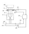
図1は、本発明による第1の実施の形態である走査型投影光学系10の概略構成図である。図中、第1面であるパターンの形成された面101を下側に向けてレチクルステージ151(図3参照)上に保持されたレチクルRの下方に、第1結像光学系100が配置されている。
【0023】
第1結像光学系100は、レチクルR側から、屈折光学系である正の屈折力を有する第1レンズ群G1、屈折光学系である負の屈折力を有する第2レンズ群G2、そして凹面鏡102がこの順に配列されている。
【0024】
さらに第1レンズ群G1と第2レンズ群G2との間の、第1結像光学系100によって中間像IMが結像される位置とほぼ一致する位置で、かつ両レンズ群の光軸からはずれた位置に、光路偏向部材である反射鏡111が配置されている。反射鏡111は、その反射面が第1レンズ群G1と第2レンズ群G2の光軸に対してほぼ45度をなすように置かれている。
【0025】
さらに、反射鏡111により偏向された光路に沿って第2結像光学系120が配置されている。
【0026】
第2結像光学系120は、反射鏡111の側から、屈折光学系である正の屈折力を有する第3レンズ群G3、やはり屈折光学系である正の屈折力を有する第4レンズ群G4がこの順に配列されて構成されており、第2結像光学系120に関して中間像IMと共役な位置に、第2面である基板の被露光面122を第4レンズ群G4の方に向けて、基板であるウエハWが置かれるようになっている。ウエハWはウエハステージ152(図3参照)上に保持されるように構成されている。
【0027】
第3レンズ群G3と第4レンズ群G4との間の瞳の位置には、開口絞りASが配置され、第3レンズ群G3と開口絞りASとの間には、偏光面を変化させる第1偏光手段である波長板121が、第3レンズ群G3と第4レンズ群G4の光軸に直角に置かれている。なお、第1偏光手段である波長板121を置く位置は、第3レンズ群G3と開口絞りASとの間に限らず、光路偏向部材である反射鏡111と第2面122との間ならどこでもよい。
【0028】
波長板121は、4分の1波長(λ/4)板や2分の1波長(λ/2)板である。この波長板121により、ウエハWの被露光面122に入射する光を円偏光にする。4分の1波長板と2分の1波長板は、次のように使い分ける。
【0029】
第1面であるレチクル面101で直線偏光であるときは、偏向鏡111の後の状態はやはり直線偏光であり、第1偏光手段121を4分の1波長板とすれば、直線偏光が円偏光に変化され、第2面であるウエハ面122に入射する光は円偏光となる。
【0030】
次に、第1面であるレチクル面101で円偏光であるときは、偏向鏡111の後の状態は一般には楕円偏光となり、第1偏光手段121を2分の1波長板とすれば、楕円偏光が円偏光に変化され、第2面であるウエハ面122に入射する光は円偏光となる。
【0031】
本実施の形態では、第1レンズ群G1、第2レンズ群G2、第3レンズ群G3、第4レンズ群G4は、硝材として合成石英あるいは蛍石、または合成石英と蛍石とを併せて用いている。合成石英と蛍石を用いた場合の作用については後述する。
【0032】
レチクルステージ151とウエハステージ152とは、相対的に同期して走査される。即ち図3において、投影光学系10の光軸方向をZ、Z軸に直交する平面内の直交座標系であるXY座標を、図中紙面に直角な方向にX軸、紙面内右方向にY軸をとると、レチクルステージ151がYの正の方向に移動するとき、ウエハステージ152はYの負方向に移動する。
【0033】
レチクルステージ151の移動は、レチクルステージ駆動装置153により行われ、レチクルステージ151の位置はレチクルステージ干渉計154により検出される。
【0034】
ウエハステージ152の移動は、ウエハステージ駆動装置155により行われ、ウエハステージ152の位置はウエハステージ干渉計156により検出される。
【0035】
レチクルステージ干渉計154とウエハステージ干渉計156の出力は、制御装置157に入力され、制御装置157から出力される制御信号が、レチクルステージ駆動装置153とウエハステージ駆動装置155に入力され、所定の同期速度でお互いに相対的に走査される。
【0036】
レチクルステージ151の上方には、照明光学系158が設けられている。
【0037】
このように構成された走査型投影光学系の作用を説明する。照明光学系158により均一に照明されたレチクルRの面101上のパターンからの光は、第1レンズ群G1と第2レンズ群G2を透過して凹面鏡102に到る。凹面鏡102で反射された光は、第2レンズ群G2を再度透過した後、反射鏡111の置かれた位置付近に中間像IMを結像する。
【0038】
このようにして反射鏡111に入射した光は偏向され、第3レンズ群G3を透過し、波長板121で偏光面を変化され、開口絞りASにより照明σ値が決定され、さらに第4レンズ群G4を介してウエハWの面122に入射する。即ち、中間像IMは面122に結像する。このとき、波長板121の作用により、面122に入射する光は円偏光にされる。したがって、レチクルRのパターンの方向性によるウエハ面122上への結像性能の劣化を防ぐことができる。これが円偏光でないとすると、レチクルRのパターンの縦横ラインの太さの均一性が崩れる。
【0039】
また、屈折光学系の硝材として合成石英と蛍石が選択されて用いられているので、300nm以下といった短い波長の照明光を使用しても光の吸収を抑えることができ、高い解像度の投影露光に適している。
【0040】
石英と蛍石の硝材としての光の分散の違いを利用して、これらを用いた屈折光学系の色収差を補正するが、両者のアッベ数はあまり離れていないので、これらを用いたレンズだけでは色収差の補正が難しい。即ちあまりにも多くのレンズを必要とするため、光学系が大きくなりすぎる。
【0041】
しかしながら、本実施の形態の投影光学系10は反射光学系である凹面鏡102を含んでおり、反射光学系は色収差がなく、レンズとは逆のペッツバール和への寄与を示すため、反射光学系と屈折光学系とを組み合わせた反射屈折光学系である本実施の形態の光学系では、レンズ枚数の増加を招くことなく、色収差をはじめ諸収差を補正し、全体としてほぼ無収差にすることができる。このようにして、実用的な大きさで、集積度の高い半導体素子の製造に求められる極めて高い光学性能を達成することができる。
【0042】
このように本発明の実施の形態によれば、紫外線波長等の短波長域で大きな開口数を達成し、光学系が実用的な大きさで、レチクルパターンの方向性に依存しない、クオーターミクロン単位の解像度を有する反射屈折光学系を備える走査型投影光学系及びそのような走査型投影光学系を備える投影露光装置を提供することができる。
【0043】
また、反射鏡111は第1結像光学系100の光軸からはずれた位置に置かれているので、レチクルRのパターンの投影には、光軸を含まないスリット状もしくは円弧状の露光領域が用いられ、レチクルRと結像面にあるウエハWとを同期走査して大きな露光領域を得る走査型投影光学系で、偏光ビームスプリッタ等の透過反射面を用いずに光路分割を実現することができる。
【0044】
すなわち、リング視野光学系は、光軸を含まないスリット状もしくは円弧状の視野を用い、物体面と結像面を同時に走査して大きな露光領域を得る、所謂ステップ・アンド・スキャン方式を採用し、中間像を作ってその付近に光路偏向部材を配置することで、ビームスプリッターを用いなくとも光路分割が実現できる。
【0045】
また、大きな開口数を得る場合でも、光路偏向部材として反射膜のコーティングされた平面鏡を用いる必要がない。したがって、平面反射鏡におけるP偏光とS偏光で反射率が違い、特に露光波長が短くなると膜材料の減少等で反射膜によるP偏光とS偏光で反射率が違ってくるが、それらの違いによる、方向性をもった偏光光の心配もない。
【0046】
投影露光に方向性をもった偏光光を用いるとレチクルパターンの方向性により結像性能が変化してしまい、特に結像側で大きな開口数をもつ場合に大きな問題となるが、この結像性能の変化も防止できる。
【0047】
また、第1結像光学系100に入射する光を直線偏光等の偏光光にすれば、光路偏向部材111等で生まれる方向性を予めコントロールし、光路偏向部材111と第2面122の間の光路中に、前記のように第1偏光手段121であるλ/4波長板等を配置することで容易に方向性の全くない円偏光で第2面122上に像を結像させることができる。
【0048】
第1結像光学系100に入射する光を直線偏光等の偏光光にするには、照明光学系158の光源(不図示)としてレーザーを用いる他、偏光子を通した光を用いる方法がある。
【0049】
図1では、第1偏光手段121は第3レンズ群G3と開口絞りASとの間に置かれているが、光路偏向部材111と第2面122との間であればよく、例えば開口絞りASと第4レンズ群G4との間、あるいは光路偏向部材111と第3レンズ群G3との間、さらには第4レンズ群と第2面122との間であっても同様な効果が得られる。但し、第3レンズ群G3と第4レンズ群G4との間が好ましい。
【0050】
図2を参照して、本発明による第2の実施の形態である走査型投影光学系11を説明する。図2はその概略構成図である。図中、偏光面を変化させる第2偏光手段131が第2レンズ群G2と光路偏向部材111との間に設けられている。その他の構成は図1の実施の形態と同様である。
【0051】
第2偏光手段131の作用を説明する。光路偏向部材111の反射面の光量損失を考えると、光は反射面に対してS偏光で入射することが望ましい。第2偏光手段131は偏光子であればよいが、典型的には偏光板が用いられ、光路偏向部材111に入射する光をS偏光の直線偏光に変化させる。あるいは4分の1波長板または2分の1波長板を用いてもよい。このようにして、光路偏向部材111での光量損失を最小限に抑える。
【0052】
なお、本実施の形態では、第2偏光手段131は、図2に示されるように光路偏向部材111の直前に設けられた偏光板であるが、これに限らず、第1面101と光路偏向部材111の間の光路中に設けて、要は光路偏向部材111に入射する光をほぼS偏光の直線偏光にするように構成すればよい。また光量損失を抑えるということは、反射面に貼り付けられる反射膜の損傷を防止することにもつながる。
【0053】
以上のように、本発明の実施の形態では、光学系の結像性能を考えると、第1結像光学系100が結像光学系であるレンズ群G1、G2と反射光学系である1枚の凹面鏡102より構成され、光路偏向部材111は平面反射鏡で、第2結像光学系120が(パワーを有する光学系として)レンズ群G3、G4のみにより構成されることが好ましく、近時の半導体製造装置にならい、第1面101の1/4〜1/6倍程度の縮小像を第2面122の上に結像させることが好ましい。また、屈折光学系であるレンズの硝材としては、合成石英、蛍石を用いるのが好ましい。
【0054】
なお、実際の走査型投影光学系としては、特開平8−334695に開示された光学系等がある。
【0055】
次に、第3の実施の形態である投影露光装置は、図3に示されるように走査型投影光学系10と、第1面101を有するレチクルRを保持するレチクルステージ151と、第2面122を有する基板Wを保持する基板ステージ152とを備える。図3は、投影光学系10が用いられる場合を示しているが、投影光学系11に置き換えてもよい。
【0056】
図3に示される投影露光装置では、ウエハWの面122とレチクルRの面101とは平行に配置されているが、このような配置は、図1あるいは図2の投影光学系において、第2結像光学系120のいずれかの位置に偏向ミラーを設置して、光軸を直角に下方に折り曲げることにより実現できる。
【0057】
図3に示されるような走査型投影露光装置を用いることによって、第1と第2の実施の形態について説明したように、レチクルR上の微細なパターンをウエハのような基板W上に転写し、あるいは大きいプレートのような基板W上に転写して集積度の高い素子を製造することができる。
【0058】
以上のように、例えば半導体素子、または液晶表示素子等をフォトリソグラフィ工程で製造する際に使用される投影露光装置の光学系に関し、特に光学系の要素として反射系を用いることにより、紫外線波長域でクオーターミクロン単位の解像度を有する反射屈折光学系とそのような光学系を備える投影露光装置を実現することができる。
【0059】
【発明の効果】
以上のように本発明によれば、屈折光学系と凹面鏡とを含み、結像に第1結像光学系の光軸からはずれた露光領域の光を用い、第1偏光手段を用いるように構成しているので、レチクルパターンの方向性に依存せず、高い解像度を有し、しかも実用的な大きさの走査型投影光学系及びそのような投影光学系を備える投影露光装置が得られる。
【図面の簡単な説明】
【図1】 本発明の第1の実施の形態である走査型投影光学系の概略構成図である。
【図2】 本発明の第2の実施の形態である走査型投影光学系の概略構成図である。
【図3】 本発明の第3の実施の形態である投影露光装置の概略構成図である。
【符号の説明】
10、11 走査型投影光学系
100 第1結像光学系
101 第1面
102 凹面鏡
111 光路偏向部材
120 第2結像光学系
121 第1偏光手段
122 第2面
131 第2偏光手段
151 レチクルステージ
152 ウエハステージ
153 レチクルステージ駆動手段
154 レチクルステージ干渉計
155 ウエハステージ駆動手段
156 ウエハステージ干渉計
157 制御装置
158 照明光学系[0001]
BACKGROUND OF THE INVENTION
The present invention relates to a projection optical system, a projection exposure apparatus, and a scanning projection exposure method , and more particularly to a projection optical system including a catadioptric optical system, a projection exposure apparatus, and a scanning projection exposure method used in a short wavelength region.
[0002]
[Prior art]
Japanese Patent Publication No. 7-1111512 and USP-4,779,966 are examples of conventional technologies of a practically sized optical system that realize a relatively large numerical aperture among the conventionally disclosed catadioptric optical systems. It is done. The catadioptric optical systems disclosed in these are so-called step-and-scan systems that use a slit-shaped or arc-shaped field of view that does not include an optical axis, and simultaneously scan the object surface and the imaging surface to obtain a large exposure area. Is used, and an intermediate image is formed and an optical path deflecting member is disposed in the vicinity thereof, thereby realizing optical path division without using a beam splitter.
[0003]
[Problems to be solved by the invention]
However, in such an optical system, one or a plurality of plane reflecting mirrors coated with a reflecting film are used as the optical path deflecting member. In such a case, the reflectivity of the plane reflecting mirror is different between P-polarized light and S-polarized light. In particular, when the exposure wavelength is shortened, the difference in reflectance between P-polarized light and S-polarized light due to the reflecting film can be eliminated due to a decrease in film material. This results in the generation of polarized light with directionality. When polarized light having directionality is used for projection exposure, the imaging performance changes depending on the directionality of the reticle pattern. In particular, when the image forming side has a large numerical aperture, this change in image forming performance becomes a significant problem.
[0004]
In view of the above, the present invention achieves a large numerical aperture in the ultraviolet wavelength region, and the catadioptric optical system having a resolution in quarter micron units, which has a practical size and does not depend on the directionality of the reticle pattern. It is another object of the present invention to provide a projection exposure apparatus including the optical system.
[0005]
[Means for Solving the Problems]
In order to achieve the above object, the projection optical system according to the first aspect of the present invention scans the
[0006]
The exposure area deviated from the optical axis is, for example, a slit-shaped or arc-shaped exposure area that does not include the optical axis. The relative scanning of the
[0007]
If comprised in this way, since the optical path deflection |
[0008]
The projection optical system includes a circularly polarized light supplying unit that illuminates the
[0009]
The projection optical system according to claim 1 includes linearly polarized light supplying means for illuminating the
[0010]
If comprised in this way, the directionality produced with the optical path deflection |
[0011]
According to a fourth aspect of the present invention, in the projection optical system described above , the second polarizing means that linearly polarizes light incident on the optical
[0012]
With this configuration, the second polarizing means 131 converts the light into linearly polarized light before entering the optical
[0013]
In order to achieve the above object, the projection optical system according to the fifth aspect of the present invention scans the
[0014]
As described in claim 6, the projection optical system according to claim 5 may further include a polarizing plate or a
[0015]
In the above projection optical system , as described in claim 7 , the second imaging
[0016]
Above the projection optical system, as set forth in claim 8, wherein the refractive optical system may have a lens made of glass material comprising quartz and fluorite.
[0017]
If comprised in this way, since the glass material has a lens containing quartz and a lens containing fluorite, it can be used even for light having a short wavelength, for example, 300 nm or less, and also has a concave mirror, so that the Abbe numbers are mutually different. Even near quartz and fluorite, correction of chromatic aberration is easy.
[0018]
The above projection optical system may be configured such that the first imaging optical system 100 is arranged following the
[0019]
A projection exposure apparatus according to a tenth aspect includes, for example, a projection
[0020]
A scanning projection exposure method according to an eleventh aspect of the invention is directed to a substrate W having a
[0021]
DETAILED DESCRIPTION OF THE INVENTION
Embodiments of the present invention will be described below with reference to the drawings. In addition, in each figure, the same code | symbol is attached | subjected to the mutually same or equivalent member, and the overlapping description is abbreviate | omitted.
[0022]
FIG. 1 is a schematic configuration diagram of a scanning projection
[0023]
The first imaging optical system 100 includes, from the reticle R side, a first lens group G1 having a positive refractive power that is a refractive optical system, a second lens group G2 having a negative refractive power that is a refractive optical system, and a concave mirror. 102 are arranged in this order.
[0024]
Furthermore, the position between the first lens group G1 and the second lens group G2 is substantially the same as the position at which the intermediate image IM is formed by the first imaging optical system 100, and deviates from the optical axes of both lens groups. The reflecting
[0025]
Further, the second imaging
[0026]
The second imaging
[0027]
An aperture stop AS is disposed at the position of the pupil between the third lens group G3 and the fourth lens group G4, and a first polarization plane is changed between the third lens group G3 and the aperture stop AS. A
[0028]
The
[0029]
When a linearly polarized light in the
[0030]
Then, when a circularly polarized light at the
[0031]
In the present embodiment, the first lens group G1, the second lens group G2, the third lens group G3, and the fourth lens group G4 use synthetic quartz or fluorite, or synthetic quartz and fluorite in combination as a glass material. ing. The effect of using synthetic quartz and fluorite will be described later.
[0032]
[0033]
The movement of
[0034]
The
[0035]
Outputs of
[0036]
An illumination
[0037]
The operation of the thus configured scanning projection optical system will be described. The light from the pattern on the
[0038]
Thus, the light incident on the reflecting
[0039]
In addition, since synthetic quartz and fluorite are selected and used as the glass material for the refractive optical system, light absorption can be suppressed even when illumination light with a short wavelength of 300 nm or less is used, and high-resolution projection exposure is possible. Suitable for
[0040]
Using the difference in the dispersion of light between quartz and fluorite glass materials, the chromatic aberration of the refractive optical system using these is corrected, but the Abbe number of both is not so far away, so only with lenses using these It is difficult to correct chromatic aberration. That is, since too many lenses are required, the optical system becomes too large.
[0041]
However, the projection
[0042]
As described above, according to the embodiment of the present invention, a large numerical aperture is achieved in a short wavelength region such as an ultraviolet wavelength, and the optical system has a practical size and does not depend on the directionality of the reticle pattern. A scanning projection optical system including a catadioptric optical system having a resolution of 1 mm and a projection exposure apparatus including such a scanning projection optical system can be provided.
[0043]
Further, since the reflecting
[0044]
In other words, the ring field optical system employs a so-called step-and-scan method that uses a slit-shaped or arc-shaped field that does not include an optical axis, and simultaneously scans the object surface and the imaging surface to obtain a large exposure area. By creating an intermediate image and arranging an optical path deflecting member in the vicinity thereof, optical path division can be realized without using a beam splitter.
[0045]
Even when obtaining a large numerical aperture, there is no need to use a coated plane mirror reflective film as an optical path deflecting direction member. Therefore, the reflectivity is different between the P-polarized light and the S-polarized light in the plane reflecting mirror. Particularly, when the exposure wavelength is shortened, the reflectivity is different between the P-polarized light and the S-polarized light due to the reduction of the film material. There is no worry about polarized light with directionality.
[0046]
If polarized light with directionality is used for projection exposure, the imaging performance changes due to the directionality of the reticle pattern, and this is a big problem especially when the imaging side has a large numerical aperture. Can also be prevented.
[0047]
Further, if the light incident on the first imaging optical system 100 is changed to polarized light such as linearly polarized light, the directionality generated by the optical
[0048]
To the light incident on the first imaging optical system 100 to the polarized light such as linearly polarized light, except for using a laser as a light source of the illumination optical system 158 (not shown), a method using a light through the polarizing child is there.
[0049]
In FIG. 1, the first
[0050]
A scanning projection
[0051]
The operation of the second
[0052]
In the present embodiment, the second
[0053]
As described above, in the embodiment of the present invention, considering the imaging performance of the optical system, the first imaging optical system 100 is a lens group G1, G2 that is an imaging optical system and one sheet that is a reflection optical system. It is preferable that the optical
[0054]
As an actual scanning projection optical system, there is an optical system disclosed in JP-A-8-334695.
[0055]
Next, as shown in FIG. 3, the projection exposure apparatus according to the third embodiment includes a scanning projection
[0056]
In the projection exposure apparatus shown in FIG. 3, the
[0057]
By using a scanning projection exposure apparatus as shown in FIG. 3, a fine pattern on the reticle R is transferred onto a substrate W such as a wafer as described in the first and second embodiments. Alternatively, a highly integrated device can be manufactured by transferring onto a substrate W such as a large plate.
[0058]
As described above, for example, an optical system of a projection exposure apparatus used when manufacturing a semiconductor element, a liquid crystal display element, or the like in a photolithography process, in particular, an ultraviolet wavelength region by using a reflection system as an element of the optical system. Thus, it is possible to realize a catadioptric optical system having a resolution of a quarter micron unit and a projection exposure apparatus including such an optical system.
[0059]
【The invention's effect】
As described above, the present invention includes the refractive optical system and the concave mirror, and uses the light in the exposure region deviated from the optical axis of the first imaging optical system for imaging, and uses the first polarizing means. Therefore, a scanning projection optical system having a high resolution and a practical size irrespective of the directionality of the reticle pattern and a projection exposure apparatus including such a projection optical system can be obtained.
[Brief description of the drawings]
FIG. 1 is a schematic configuration diagram of a scanning projection optical system according to a first embodiment of the present invention.
FIG. 2 is a schematic configuration diagram of a scanning projection optical system according to a second embodiment of the present invention.
FIG. 3 is a schematic block diagram of a projection exposure apparatus according to a third embodiment of the present invention.
[Explanation of symbols]
DESCRIPTION OF
Claims (11)
第1面の中間像を形成する第1結像光学系と;
前記中間像の像を前記第2面上に形成する第2結像光学系と;
前記中間像の近傍に配置され、前記第1結像光学系からの光を前記第2結像光学系へ導く光路偏向部材と;
前記光路偏向部材と前記第2面との間の光路中に配置され、偏光面を変化させる第1偏光手段とを備え;
前記第1結像光学系は、屈折光学系と凹面鏡とを含み;
前記第1結像光学系は、前記結像に該第1結像光学系の光軸からはずれた露光領域の光を用いるように構成されたことを特徴とする;
投影光学系。In a projection optical system used in a scanning projection exposure apparatus that relatively scans a first surface and a second surface and forms an image of the first surface on the second surface;
A first imaging optical system for forming an intermediate image of the first surface;
A second imaging optical system for forming an image of the intermediate image on the second surface;
Wherein arranged in the vicinity of the intermediate image, and an optical path deflecting member for guiding light from the first imaging optical system to the second imaging optical system;
A first polarizing means disposed in an optical path between the optical path deflecting member and the second surface and changing a polarization plane;
The first imaging optical system includes a refractive optical system and a concave mirror;
The first imaging optical system is configured to use light in an exposure region deviated from an optical axis of the first imaging optical system for the imaging;
Projection optics .
前記第1偏光手段は2分の1波長板であることを特徴とする、請求項1に記載の投影光学系。Circularly polarized light supplying means for illuminating the first surface with circularly polarized light;
The projection optical system according to claim 1, wherein the first polarizing unit is a half-wave plate.
前記第1偏光手段は4分の1波長板であることを特徴とする、ことを特徴とする、請求項1に記載の投影光学系。Linearly polarized light supplying means for illuminating the first surface with linearly polarized light;
It said first polarizing means, characterized in that a quarter wave plate, and wherein the projection optical system according to claim 1.
屈折光学系と凹面鏡とを含み、前記第1面の中間像を形成する第1結像光学系と; A first imaging optical system that includes a refractive optical system and a concave mirror and forms an intermediate image of the first surface;
前記中間像の像を前記第2面上に形成する第2結像光学系と; A second imaging optical system for forming an image of the intermediate image on the second surface;
前記中間像の近傍に配置され、前記第1結像光学系からの光を前記第2結像光学系へ導く光路偏向部材とを備え; An optical path deflecting member that is disposed in the vicinity of the intermediate image and guides light from the first imaging optical system to the second imaging optical system;
前記第1結像光学系は、前記結像に前記第1結像光学系の光軸からはずれた露光領域の光を用いるように構成され; The first imaging optical system is configured to use light in an exposure region deviated from an optical axis of the first imaging optical system for the imaging;
前記光路偏向部材に対してS偏光の直線偏光を前記光路偏向部材に入射させることを特徴とする; S-polarized linearly polarized light is incident on the optical path deflecting member with respect to the optical path deflecting member;
投影光学系。Projection optics.
前記第1面を有するレチクルを保持するレチクルステージと;
前記第2面を有する基板を保持する基板ステージとを備えることを特徴とする;
投影露光装置。A projection optical system according to any one of claims 1 to 9 ;
A reticle stage for holding a reticle having the first surface;
A substrate stage for holding the substrate having the second surface;
Projection exposure apparatus.
前記レチクルと前記基板とを相対的に走査する工程とを備えていることを特徴とする; A step of relatively scanning the reticle and the substrate;
走査投影露光方法。 Scanning projection exposure method.
Priority Applications (1)
| Application Number | Priority Date | Filing Date | Title |
|---|---|---|---|
| JP36274197A JP3852196B2 (en) | 1997-12-12 | 1997-12-12 | Projection optical system, projection exposure apparatus, and scanning projection exposure method |
Applications Claiming Priority (1)
| Application Number | Priority Date | Filing Date | Title |
|---|---|---|---|
| JP36274197A JP3852196B2 (en) | 1997-12-12 | 1997-12-12 | Projection optical system, projection exposure apparatus, and scanning projection exposure method |
Publications (2)
| Publication Number | Publication Date |
|---|---|
| JPH11176741A JPH11176741A (en) | 1999-07-02 |
| JP3852196B2 true JP3852196B2 (en) | 2006-11-29 |
Family
ID=18477627
Family Applications (1)
| Application Number | Title | Priority Date | Filing Date |
|---|---|---|---|
| JP36274197A Expired - Lifetime JP3852196B2 (en) | 1997-12-12 | 1997-12-12 | Projection optical system, projection exposure apparatus, and scanning projection exposure method |
Country Status (1)
| Country | Link |
|---|---|
| JP (1) | JP3852196B2 (en) |
Families Citing this family (2)
| Publication number | Priority date | Publication date | Assignee | Title |
|---|---|---|---|---|
| JP2006173305A (en) * | 2004-12-15 | 2006-06-29 | Canon Inc | Aligner and its method, and device manufacturing method |
| JP6936002B2 (en) * | 2016-12-08 | 2021-09-15 | リコーインダストリアルソリューションズ株式会社 | Projection optics and projection equipment and imaging equipment |
-
1997
- 1997-12-12 JP JP36274197A patent/JP3852196B2/en not_active Expired - Lifetime
Also Published As
| Publication number | Publication date |
|---|---|
| JPH11176741A (en) | 1999-07-02 |
Similar Documents
| Publication | Publication Date | Title |
|---|---|---|
| US6466303B1 (en) | Projection exposure apparatus with a catadioptric projection optical system | |
| US9778576B2 (en) | Microlithography illumination system and microlithography illumination optical unit | |
| US7236254B2 (en) | Exposure apparatus with interferometer | |
| US5241423A (en) | High resolution reduction catadioptric relay lens | |
| US5089913A (en) | High resolution reduction catadioptric relay lens | |
| US7961298B2 (en) | Polarization rotator and a crystalline-quartz plate for use in an optical imaging system | |
| JP2003077827A (en) | Microlithographic illumination method and projection lens for carrying out the same | |
| JPH04232951A (en) | Face state inspecting device | |
| US9046787B2 (en) | Microlithographic projection exposure apparatus | |
| US20100277708A1 (en) | Illumination system of a microlothographic projection exposure apparatus | |
| US7573563B2 (en) | Exposure apparatus and device manufacturing method | |
| JP2002222754A (en) | Correcting device, aligner, method of manufacturing device, and device | |
| US7511826B2 (en) | Symmetrical illumination forming system and method | |
| JPH0822948A (en) | Scanning aligner | |
| JPH09246160A (en) | Exposing aligner | |
| JP3852196B2 (en) | Projection optical system, projection exposure apparatus, and scanning projection exposure method | |
| JP3352325B2 (en) | Scanning exposure apparatus and device manufacturing method using the same | |
| JP2000147382A (en) | Polarization optical correction objective lens | |
| JP2005531021A (en) | Catadioptric reduction objective lens | |
| KR101699639B1 (en) | Optical system for a microlithographic projection exposure apparatus and microlithographic exposure method | |
| CN102884480A (en) | Illumination system of a microlithographic projection exposure apparatus | |
| JP2007287885A (en) | Illuminating optical apparatus, aligner, and method of manufacturing device | |
| US8149380B2 (en) | Exposure apparatus and correction apparatus | |
| JPH09237753A (en) | Projection aligner | |
| JPH0722350A (en) | Aligner and manufacture of element using the same |
Legal Events
| Date | Code | Title | Description |
|---|---|---|---|
| A621 | Written request for application examination |
Free format text: JAPANESE INTERMEDIATE CODE: A621 Effective date: 20041130 |
|
| A521 | Written amendment |
Free format text: JAPANESE INTERMEDIATE CODE: A523 Effective date: 20050228 |
|
| A977 | Report on retrieval |
Free format text: JAPANESE INTERMEDIATE CODE: A971007 Effective date: 20060809 |
|
| TRDD | Decision of grant or rejection written | ||
| A01 | Written decision to grant a patent or to grant a registration (utility model) |
Free format text: JAPANESE INTERMEDIATE CODE: A01 Effective date: 20060815 |
|
| A61 | First payment of annual fees (during grant procedure) |
Free format text: JAPANESE INTERMEDIATE CODE: A61 Effective date: 20060828 |
|
| R150 | Certificate of patent or registration of utility model |
Free format text: JAPANESE INTERMEDIATE CODE: R150 |
|
| FPAY | Renewal fee payment (event date is renewal date of database) |
Free format text: PAYMENT UNTIL: 20090915 Year of fee payment: 3 |
|
| FPAY | Renewal fee payment (event date is renewal date of database) |
Free format text: PAYMENT UNTIL: 20120915 Year of fee payment: 6 |