JP3847875B2 - Image forming apparatus - Google Patents
Image forming apparatus Download PDFInfo
- Publication number
- JP3847875B2 JP3847875B2 JP01749297A JP1749297A JP3847875B2 JP 3847875 B2 JP3847875 B2 JP 3847875B2 JP 01749297 A JP01749297 A JP 01749297A JP 1749297 A JP1749297 A JP 1749297A JP 3847875 B2 JP3847875 B2 JP 3847875B2
- Authority
- JP
- Japan
- Prior art keywords
- voltage
- transfer
- output
- current value
- image
- Prior art date
- Legal status (The legal status is an assumption and is not a legal conclusion. Google has not performed a legal analysis and makes no representation as to the accuracy of the status listed.)
- Expired - Fee Related
Links
Images


Landscapes
- Electrostatic Charge, Transfer And Separation In Electrography (AREA)
- Control Or Security For Electrophotography (AREA)
Description
【0001】
【発明の属する技術分野】
本発明は、電子写真感光体・静電記録誘電体・磁気記録磁性体等の像担持体に対して電子写真プロセス・静電記録プロセス・磁気記録プロセス等の適宜の作像プロセス手段により所要の画像情報に対応した可転写像(一般にトナー像)を形成担持させ、該像担持体に当接させ、かつ電圧を印加した転写部材との間に記録媒体(一般に普通紙)を通過させて像担持体側の可転写像を記録媒体側に転写せしめる接触転写方式の画像形成装置に関する。
【0002】
より詳しくは、接触転写方式の画像形成装置における転写部材に対する転写バイアス制御手段に関する。
【0003】
【従来の技術】
転写方式の画像形成装置において、像担持体に形成担持させた可転写像を記録媒体に転写させる手段としてはバイアスローラ転写が多用されている。
【0004】
これは、転写部材としての導電性の転写ローラを像担持体に接触させて配設し、かつ所定の転写バイアス(転写電圧、トナーの帯電極性と逆極性)を印加し、像担持体と転写ローラの当接ニップ部(転写ニップ部)に記録媒体を導入して転写ニップ部を挟持搬送通過させるもので、転写ニップ部において、転写ローラが接触している記録媒体背面が転写ローラに印加の転写バイアスにより帯電され、その帯電電荷の静電気力により像担持体側の可転写像が記録媒体表面側に引き寄せられて転移する。即ち像担持体側の可転写像が記録媒体側に静電転写される。
【0005】
【発明が解決しようとする課題】
ところで、転写部材としての導電性の転写ローラは環境変動や耐久により抵抗値が変化する。特に、イオン導電性転写ローラ(NBR、EPDM、ウレタン等のゴムに界面活性材などを注入したもの、もしくはイオン導電性の高分子をゴム層としたもの)のような環境の変化により抵抗値が顕著に変化するものでは、連続でプリントした場合に、転写ローラの抵抗値が変化することで、該転写ローラに印加している転写バイアス値が適切な値でなくなっていた。
【0006】
これは転写性能を悪化させプリントアウトされる画像形成物の画像品位(印字品位)を低下させる結果となる。
【0007】
そこで本発明は接触転写方式の画像形成装置について、転写部材材質の環境あるいは経時変動による物性変化での画質劣化を防止する、即ち転写部材の環境変化や耐久による抵抗値変動(物性変動)に拘わらず、プリントアウトさせる画像形成物の画像品位(印字品位)は高画質・高精彩に長期に渡って安定に維持させることを目的とする。
【0008】
【課題を解決するための手段】
本発明は下記の構成を特徴とする画像形成装置である。
【0009】
(1)トナー像を担持する像担持体と、前記像担持体と転写領域を形成し、前記転写領域において前記像担持体から転写材にトナー像を転写する転写部材と、前記転写部材に対して第1または第2の電圧を出力する電圧出力手段と、を有し、連続して複数の転写材に転写をする場合に、転写材が前記転写領域にあるときに、前記電圧出力手段が前記第1の電圧を出力して前記像担持体上のトナー像を転写材に転写し、前記転写領域に転写材が無いときに、前記電圧出力手段が前記第2の電圧を出力する画像形成装置において、
前記第1の電圧は、転写材が前記転写領域に進入する前に、前記電圧出力手段が出力電圧を変化させる過程で、前記電圧出力手段の出力電流値が予め設定したターゲット電流値と略一致したときの前記電圧出力手段の出力電圧に基づいて設定し、前記第2の電圧の出力時における前記電圧出力手段の出力電流値と、前記ターゲット電流値と、を比較した結果に基づいて前記第1の電圧を補正することを特徴とする画像形成装置。
【0010】
【0011】
【0012】
(2)前記転写部材がイオン導電性の転写部材であることを特徴とする(1)に記載の画像形成装置。
【0013】
(3)前記第1の電圧の電圧値をVt、前記電圧出力手段の出力電流値がターゲット電流値と略一致したときの前記電圧出力手段の出力電圧をVt0、α及びβを定数とした場合に、VtをVt=αVt0+βの演算に基づいて設定することを特徴とする(1)または(2)に記載の画像形成装置。
【0014】
(4)前記第2の電圧の出力時における前記電圧出力手段の出力電流値と前記ターゲット電流値とを比較した結果に基づいて、前記Vt0を補正することを特徴とする(3)に記載の画像形成装置。
【0015】
(5)前記第2の電圧の出力時における前記電圧出力手段の出力電流値と前記ターゲット電流値とを比較した結果に基づいて、前記αを補正することを特徴とする(3)または(4)に記載の画像形成装置。
【0016】
(6)前記第2の電圧の出力時における前記電圧出力手段の出力電流値と前記ターゲット電流値とを比較した結果に基づいて、前記βを補正することを特徴とする(3)から(5)のいずれか一項に記載の画像形成装置。
【0017】
【0018】
(7)前記第1の電圧から前記第2の電圧への切換えは、段階的に出力を変化させながら行うことを特徴とする(1)から(6)のいずれか一項に記載の画像形成装置。
(8)前記第2の電圧の出力時における前記電圧出力手段の出力電流値と、前記ターゲット電流値の差に応じて前記第1の電圧の補正を行うか否かを決定することを特徴とする(1)から(7)のいずれか一項に記載の画像形成装置。
【0019】
【0020】
〈作 用〉
即ち本発明は、環境の変化等に伴う転写部材の抵抗値変動を検知し、その抵抗値変動に対応して転写部材に印加する転写バイアス値を適切に補正することで、転写部材の抵抗値変動に拘わらず、該抵抗値変動の影響を低減させて、プリントアウトされる画像形成物の画像品位は高画質・高精彩に長期に渡って安定に維持させるものである。
【0021】
つまり、像担持体の前回転期間中に行う転写PTVCの他に、印字中の紙間において、紙間バイアス印加中の転写電流をモニタし、その電流値に基づき転写部材の抵抗成分(抵抗値変化)を検出し、プリントバイアス値を補正する転写バイアス制御系を有することにより、環境の変化による転写部材の抵抗値変動に影響されないプリントバイアスを得ることが可能となり、高画質、高精彩な画像が得られるといった効果につながる。
【0022】
より具体的に、本発明の画像形成装置は前記のように、転写部材にバイアスを印加する印加バイアス制御手段、転写部材に流れる電流値を検出する電流値検出手段、検出した値より補正数を算出する算出手段、連続プリントの紙間でプリントバイアスを補正する補正手段を有する制御回路を具備している。そして、紙間で定電流制御(PTVC)を行い、そこで検出された値に基づきプリントバイアスを調整するシーケンスを備えることで、プリント中に転写部材に急激な物性変動即ち抵抗値変化を生じても常にほぼ一定の高品位な印字品質を維持させることができる。
【0023】
特に、イオン導電性転写ローラ、ソリッド転写ローラのように、温度/湿度によって急激に抵抗値が変動する材質の転写部材を使用する際の画質向上に効果が大きい。
【0024】
【発明の実施の形態】
〈実施形態例1〉(図1〜図3)
(1)画像形成装置例
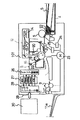
図1は本発明に従う画像形成装置の一例の概略構成図である。
【0025】
本例の画像形成装置は転写式電子写真プロセス利用のレーザプリンタ101であり、コンピュータ等の外部機器30の印字命令に従い記録紙(印字紙)Sをペーパカセットなどの記録紙格納部より給紙し、レジストローラ対等の同期搬送手段により記録紙の搬送タイミングとビデオコントローラからの画像情報送出タイミングを同期させて搬送し、画像記録を行なっている。
【0026】
17は像担持体としての回転ドラム型の電子写真感光体(以下、感光ドラムと記す)であり、矢示の時計方向に所定の周速度(プロセススピード)をもって回転駆動される。
【0027】
感光ドラム17は回転過程でその周面に、前露光器18による全面一様の前露光処理、一次帯電器19による所定の極性・電位の一様な帯電処理、レーザスキャナ12による画像情報の書き込み走査露光Lを受ける。これにより回転感光ドラム17の周面に画像情報の静電潜像が形成される。その静電潜像は現像器20によりトナー像として現像される。レーザスキャナ12は画像情報の時系列電気デジタル画素信号に対応してオン・オフ変調したレーザ光を出力して回転感光ドラム面をドラム母線方向に走査露光Lすることで画像情報の書き込みを行なう。現像器20による静電潜像の現像は、レーザプリンタにおいては、反転現像とする場合が多い。
【0028】
一方、半月型の給紙ローラ5の一回転駆動により、不図示の分離部材との協動において、記録紙格納部としてのペーパカセット4内に積載収納させた記録媒体としての記録紙Sが一枚分離給送される。
【0029】
給送された記録紙Sは、同期搬送手段としてのレジストローラ対6により感光ドラム17と転写部材としての転写ローラ21との当接ニップ部である転写ニップ部T対して感光ドラム17の回転と同期どりされた所定のタイミングで導入され、該転写ニップ部Tを挟持搬送される。
【0030】
レジストローラ対6はその回転がオン・オフ制御され、回転−オフ状態において、ペーパカセット4側から一枚分離給送された記録紙Sの先端をニップ部に受け止める。そして所定の制御タイミングで回転−オンされることで記録紙を転写ニップ部Tに送り出す。記録紙の後端がレジストローラ対6のニップ部を抜けると、レジストローラ対6は回転−オフ状態に戻される。
【0031】
半月型の給紙ローラ5は一回転すると駆動が停止されるが、一枚分離給送された記録紙はレジストローラ対6により搬送される。
【0032】
転写ローラ21には転写バイアス駆動回路200(図3)により所定に制御された転写バイアスが印加される。転写バイアス駆動回路200については後述する。転写ニップ部Tにおいて、転写ローラ21が接触している記録紙背面が転写ローラに印加の転写バイアスにより帯電され、その帯電電荷の静電気力により回転感光ドラム17側の可転写像であるトナー像が記録紙表面側に引き寄せられて転移する。即ち、転写ニップ部Tにおいて、該転写ニップ部Tを挟持搬送されていく記録紙側に感光ドラム17側のトナー像が順次に静電転写される。
【0033】
転写ニップ部Tでトナー像の転写を受けた記録紙Sは回転感光ドラム17の面から分離され、ガイド板7に案内されて定着器9(本例は熱ローラタイプ)に導入されることでトナー像の熱圧定着処理を受け、排紙ローラ11により機外の排紙トレイ11aにプリントアウトされる。
【0034】
記録紙分離後の回転感光ドラム17面はクリーニング器22にて転写残りトナー等の残存付着汚染物の除去を受けて清浄面化され、繰り返して作像に供される。
【0035】
本例のプリンタにおいては、感光ドラム17・一次帯電器19・現像器20・クリーニング器22の4つのプロセス機器をプリンタ本体に対して一括して着脱・交換自在のプロセスカートリッジ8として構成してある。
【0036】
23はプリンタのメインモータであり、感光ドラム17、給紙ローラ5、レジストローラ対6、定着器9、排紙ローラ11等を駆動する。24は給紙ローラクラッチ、25はレジストローラクラッチである。
【0037】
(2)プリンタの全体的な動作制御
26はプリンタ制御部(エンジンコントローラ)であり、タイマ、ROM、RAM等を装備したMPU(マイクロコンピュータ)及び各種入出力制御回路等で構成されている。
【0038】
このプリンタ制御部26は内部通信手段であるビデオインターフェイス27を介してビデオコントローラ部28と接続され、さらに該ビデオコントローラ部28はセントロニクスインターフェイス等の汎用インターフェイス29を介してコンピュータ等の外部機器30に接続されている。
【0039】
ビデオコントローラ部28は外部機器30から汎用インターフェイス29を介してプリンタ101に送信される画像情報をビデオ信号(VDO信号;プリンタ・エンジンが印字すべき画像信号)に変換し、ビデオインターフェイス27を介してプリント制御部26に送信する。
【0040】
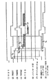
図2はこのプリンタ101の動作タイミングチャートである。
【0041】
ビデオコントローラ部28は、RDY信号(プリンタ・エンジンがプリント信号を受ければ印字を開始もしくは継続できることを示す信号、コマンドとステータスをやりとりするための信号)がTRUE(理論が真)であることを確認するとPRINT信号をTRUEとする。
【0042】
プリンタ制御部26は、PRINT信号がTRUEとなると、メインモータ23、およびレーザスキャナ12のポリゴンモータ14の駆動を開始する。13は半導体レーザである。メインモータ23の駆動で、感光ドラム17、定着器9の定着ローラ、排紙ローラ11等が回転する。この後、前露光器18、一次帯電器19、現像器20、転写ローラ21等の駆動制御や高圧印加制御も順次行なわれる。
【0043】
またプリンタ制御部26は、ポリゴンモータ14の駆動開始から該モータの回転が定常状態となるT1秒に給紙ローラクラッチ24をオンして給紙ローラ5を駆動し、記録紙Sをレジストローラ対6に向けて給紙する。そして、プリンタ制御部26は、記録紙Sの先端がレジストローラ対21に到達するタイミングでVSREQ信号(プリントシーケンスを実行するための信号、プリンタ・エンジンが印字の準備を完了したことを知らせる信号)をビデオコントローラ部28に送出すると共に、給紙ローラクラッチ24のオンからT2秒後に給紙ローラクラッチ24をオフし、給紙ローラ5の駆動を停止する。
【0044】
ビデオコントローラ部28は、画像情報のドットイメージへの展開を終えてVDO信号の出力の準備が完了すると、VSREQ信号がTRUEであることを確認し、VSYNC信号(垂直方向(ドラム回転方向)の同期信号)をTRUEとし、これを同期してTv後に1頁文の画像データとしてのVDO信号の出力を開始する。
【0045】
この時、プリンタ制御部26は、VSYNC信号の立上がりからT3秒後にレジストローラクラッチ25をオンし、レジストローラ対6を駆動している。レジストローラ対6の駆動は、記録紙Sの後端がレジストローラ対6を通過するまでの時間T4秒間行なわれる。
【0046】
また、この間プリンタ制御部26は、VSYNC信号をレーザ走査に同期した所定タイミングでビデオコントローラ部28に送出すると共に、VDO信号に基づいて感光ドラム17面を走査するレーザ光を変調する。
【0047】
また、更に次頁のプリントを行なう場合は、T5秒後に再びPRINT信号をTRUEとする。その後は1頁目と同様の動作が行われる。
【0048】
このようなプリンタ制御部26およびビデオコントローラ部28の動作により、記録紙Sは給紙ローラ5→レジストローラ対6→転写ニップ部T→ガイド板7→定着器9→排紙ローラ11の経路を順次搬送され、画像記録がなされる。
【0049】
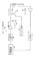
(3)転写バイアス駆動回路200
図3は転写部材である転写ローラ21(転写部材)に対して転写バイアスを印加する転写バイアス駆動回路200を示している。
【0050】
この転写バイアス駆動回路200は、電流制御回路(PWM回路)201(電流検出手段からの検出情報に基づき、電圧出力手段の出力電圧を制御する電圧制御手段)、D/A変換器(LPF)202、増幅器203、スイッチング回路204、トランス205(転写部材に印加する電圧値を出力する電圧出力手段)、モニタ回路206、A/D変換器207(電圧出力手段により出力された電圧により転写部材に流れる電流をモニタする電流検出手段)等から構成されている。
【0051】
転写バイアスは転写ローラ21の抵抗値に応じた最適な値がある。そのため、転写バイアス駆動回路200では、転写ローラ21の抵抗値を検知し、最適の印加電圧を算出するための定電流制御を行っている。
【0052】
この定電流制御の動作を述べると、まず電流制御回路201でA/D変換器207からのフィードバック信号に応じた電圧V1をコンデンサ209にチャージし、この電圧V1をスイッチング回路204にてスイッチングする。
【0053】
このスイッチング回路204の動作に応じて、トランス205が駆動し、転写電圧が出力され、転写ローラ21に印加される。
【0054】
転写ローラ21に流れる電流値はモニタ回路206で電圧信号に変換される。電圧値として取り出された転写電流値はA/D変換器207でフィードバック信号となる。電流制御回路201はフィードバック信号をモニタしながら規定量に達するまでPWM信号のレベルを上げていく、といった定電流制御を行っている。
【0055】
そして、この定電流制御の一連の動作を、転写ローラ21の抵抗値を周囲数ポイントで測定し平均を行うため、プリンタの前回転期間時、即ちプリンタのスタンバイ状態において印字スタート信号に基づいて感光ドラム17の回転が開始されてから実際に画像形成(印字)が開始されるまでの感光ドラム回転期間時に行っている。
【0056】
プリンタ制御部26はビデオコントローラ部28のプリント要求を検出すると転写バイアス出力値の初期設定を行う。これは感光ドラム17に流れる転写電流値が予め設定したIt0(ターゲット電流)となるようなバイアスVt0(ターゲット電流検知時電圧)を検出し、印字開始まで出力する。検出方法は上述したとおりである。
【0057】
VSYNC信号出力後、記録紙先端が感光ドラム17と転写ローラ21の当接ニップ部である転写ニップ部Tに突入するタイミングでプリントバイアス算出式
Vt=αVt0+β・・・・算出式1
から求めたVtを出力する。Vtは、記録紙Sの抵抗を考慮し、感光体ドラム17に乗ったトナーを記録紙Sに転写するために必要な転写電流を上乗せした転写電圧値(転写バイアス)である。
【0058】
転写バイアスV tは印字終了後、記録紙後端が転写ニップ部Tを通過するまで印加し、その後、バイアスVt0に切り換える。
【0059】
このように連続プリント時は、印字する記録紙Sが転写ニップ部Tを通過しているときは転写バイアスをV t、紙間はV 0 (紙間電圧)というサイクルで転写バイアスの出力値を切り換えている。
【0060】
(4)転写バイアスV tの補正
連続プリント時、転写ローラ21の昇温により転写ローラの抵抗値が変化し、所望の転写バイアスV tが得られなくなる。したがって、本例では連続プリント時の紙間でプリント時に必要な転写バイアスV tを転写ローラの抵抗値に以下に述べる方法で補正する。
【0061】
本例では、紙間で転写ローラ21にバイアスV 0 (≒V t0 )を印加した状態で、感光体ドラム17に流れる電流値Iをモニタし、その結果から転写バイアスV tの補正を実行するか否かを決定する。
【0062】
本来、紙間で検出する電流値Iは、プリント開始時に転写電流がIt0となるべくして求めた電圧値Vt0であるため、
I=It0
となるはずである。
【0063】
しかし、連続プリント時は転写ローラ21は昇温等の影響により抵抗値が変化するために
I≠I t0
となる。
【0064】
したがって、紙間で転写電流値Iをモニタし、It0との差分が±A%を越えた場合は補正を行い、差分が±A%以内であれば補正は行わない。
【0065】
転写バイアスV tの補正は、補正動作実行の可否条件となるIt0との基準となる差分Aに応じた電圧値を転写バイアスVtに加算することで行う。
【0066】
このように毎紙間で感光体ドラム17を流れる転写電流値Iと所望の値を比較し、所定量以上のずれを検出した場合は初期転写バイアス初期値Vt0を補正することで、連続プリント時に発生する転写ローラ21の抵抗値変化によって発生するプリント時の転写バイアスのずれを補正する。
【0067】
〈実施形態例2〉
本例においては、転写バイアスV tの補正は、紙間で転写電流値Iをモニタし、I≠I t0となった場合は、It0とIの差分に応じた電圧値をV tに加算する。その他の事項は実施形態例1と同様である。
【0068】
このように毎紙間で感光体ドラム17を流れる転写電流値Iと所望の値を比較し、一致しない場合は転写バイアスV tを補正することで、連続プリント時に発生する転写ローラ21の抵抗値変化によって発生するプリント時の転写バイアスのずれを補正する。
【0069】
〈実施形態例3〉
本例においては、転写バイアスV tの補正は、補正動作実行の可否条件となるIt0との基準となる差分Aに応じた電圧値β、即ち前述したプリントバイアス算出式1のβに加算することで行う。その他の事項は実施形態例1と同様である。
【0070】
このように毎紙間で感光体ドラム17を流れる転写電流値Iと所望の値を比較し、所定量以上のずれを検出した場合はプリントバイアス算出式1のβを補正することで、連続プリント時に発生する転写ローラ21の抵抗値変化によって発生するプリント時の転写バイアスのずれを補正する。
【0071】
なお、本例では差分Aを基準としたが、所定の基準を設けずに、It0とIの差分に応じた電圧値をβに加算しても良い。
【0072】
〈実施形態例4〉
本例においては、転写バイアスV tの補正は、補正動作実行の可否条件となるIt0との基準となる差分Aに応じて、前述したプリントバイアス算出式1の係数αの補正を行う。その他の事項は実施形態例1と同様である。
【0073】
このように毎紙間で感光体ドラム17を流れる転写電流値Iと所望の値を比較し、所定量以上のずれを検出した場合はプリントバイアス算出式1の係数αを補正することで、連続プリント時に発生する転写ローラ21の抵抗値変化によって発生するプリント時の転写バイアスのずれを補正する。
【0074】
なお、本例では差分Aを基準としたが、所定の基準を設けずに、It0とIの差分に応じて係数αを補正しても良い。
【0075】
〈実施形態例5〉
本例においては、転写バイアスV tの補正は、紙間で転写電流値Iをモニタし、It0との差分が所定の回数連続して±A%を越えた場合、もしくは、所定回数の検出値の平均が±A%を越えた場合は補正を行い、差分が±A%以内であれば補正は行わない。
【0076】
転写バイアスV tの補正は、補正動作実行の可否条件となるIt0との基準となる差分Aに応じた電圧値を実施形態例1乃至4と同様の手段にて行う。
【0077】
なお、本例では差分Aを基準としたが、所定の基準を設けずに、It0とIの差分に応じて補正しても良い。
【0078】
〈実施形態例6〉(図4)
実施形態例1乃至5において、連続プリント時に、印字する記録紙が転写ニップ部Tを通過しているときは転写ローラ21に対する転写バイアスをV t、紙間はV 0というサイクルで転写バイアス出力値を切り換える際に、該転写バイアス出力の切り替え(転写バイアスV tから紙間V 0に変化)を急峻に行った場合、転写バイアス駆動回路に実在するインダクタンス成分、容量成分の影響により電流波形にアンダーシュートa(図5)が生じてしまう。そのため、連続プリント時に紙間で行う転写ローラ21の抵抗値検出の正確性が低下する。
【0079】
本例では、転写バイアス出力の切り替える際に、所定の勾配を持って段階的に出力を変化させながら最終的な値に設定する(図4参照)。このような制御を行うことで、電流波形のアンダーシュートを削除し、転写ローラ21の抵抗値検出が正確に行うことが可能となる。そしてこれにより実施形態例1ないし5において、転写バイアスV tの補正が正確に行え、画像劣化を防ぐことにつながる。
【0080】
〈その他〉
1)転写部材は回動ベルト型や走行ウエブ型などの形態のものにすることもできる。
【0081】
2)像担持体は電子写真感光体に限られず、静電記録誘電体や磁気記録磁性体等であってもよい。またドラム型に限らず、回動ベルト型や走行ウエブ型などの形態のものにすることもできる。それらの像担持体に対する可転写像の形成プロセスは任意である。
【0082】
3)記録媒体は中間転写ドラムなど中間転写媒体であってもよい。
【0083】
【発明の効果】
以上説明したように、本発明によれば、連続プリント時における転写部材の抵抗値変化による画質の変動を低減することができ、連続プリント時の画質の安定化を図れるものである。
【0084】
【図面の簡単な説明】
【図1】 画像形成装置例の概略構成図
【図2】 該画像形成装置(レーザプリンタ)の動作タイミングチャート
【図3】 転写ローラに対する転写バイアス駆動回路図
【図4】 転写バイアス出力の切り替えを所定の勾配を持って段階的に変化させて行った場合と、この場合における電流波形の図
【図5】 転写バイアス出力の切り替えを急峻に行った場合と、この場合における電流波形の図
【符号の説明】
17 像担持体としての回転感光ドラム
S 記録媒体としての記録紙
21 接触転写部材としての転写ローラ
26 プリンタ制御部
28 ビデオコントローラ部
30 コンピュータ等の外部機器
27・29 インターフェイス
200 転写バイアス駆動回路
201 電流制御回路(PWM回路)
202 D/A変換器(LPF)
203 増幅器
204 スイッチング回路
205 トランス
206 モニタ回路
207 A/D変換器
209 コンデンサ
[0001]
BACKGROUND OF THE INVENTION
The present invention requires a suitable image forming process means such as an electrophotographic process, an electrostatic recording process, and a magnetic recording process for an image carrier such as an electrophotographic photosensitive member, an electrostatic recording dielectric, and a magnetic recording magnetic body. A transferable image (generally a toner image) corresponding to image information is formed and supported, and a recording medium (generally plain paper) is passed between the image bearing member and a transfer member to which a voltage is applied. The present invention relates to a contact transfer type image forming apparatus for transferring a transferable image on a carrier side to a recording medium side.
[0002]
More specifically, the present invention relates to a transfer bias control unit for a transfer member in a contact transfer type image forming apparatus.
[0003]
[Prior art]
In a transfer type image forming apparatus, bias roller transfer is frequently used as means for transferring a transferable image formed and supported on an image carrier to a recording medium.
[0004]
This is because a conductive transfer roller as a transfer member is arranged in contact with the image carrier, and a predetermined transfer bias (transfer voltage, opposite to the toner charging polarity) is applied to transfer the image carrier to the image carrier. A recording medium is introduced into the contact nip portion (transfer nip portion) of the roller, and the transfer nip portion is nipped and conveyed. In the transfer nip portion, the back surface of the recording medium in contact with the transfer roller is applied to the transfer roller. Charged by the transfer bias, the transferable image on the image carrier side is attracted and transferred to the recording medium surface side by the electrostatic force of the charged charge. That is, the transferable image on the image carrier side is electrostatically transferred to the recording medium side.
[0005]
[Problems to be solved by the invention]
Incidentally, the resistance value of a conductive transfer roller as a transfer member changes due to environmental fluctuations and durability. In particular, the resistance value may change due to environmental changes such as an ion conductive transfer roller (NBR, EPDM, urethane or other rubber injected with a surface active material, or an ion conductive polymer rubber layer). In the case of remarkable change, when the printing is continuously performed, the transfer bias value applied to the transfer roller is not an appropriate value because the resistance value of the transfer roller changes.
[0006]
This deteriorates the transfer performance and results in a decrease in the image quality (print quality) of the printed image formed.
[0007]
Accordingly, the present invention relates to a contact transfer type image forming apparatus, which prevents image quality deterioration due to a change in physical properties due to an environment of a transfer member material or a change over time, that is, regardless of a change in resistance value (a change in physical properties) due to an environmental change or durability of the transfer member. The image quality (printing quality) of the image-formed product to be printed out is intended to be maintained stably over a long period of time with high image quality and high definition.
[0008]
[Means for Solving the Problems]
The present invention is an image forming apparatus having the following configuration.
[0009]
(1) an image bearing member for bearing a toner image, to form the image bearing member and the transfer area, a transfer member for transferring the toner image to a transfer material from said image bearing member in the transfer area, with respect to the transfer member a voltage output means for outputting the first or second voltage, and possess Te, when continuously to transfer the plurality of the transfer material, when the transfer material is in the transfer region, said voltage output means Image formation in which the first voltage is output to transfer the toner image on the image carrier onto a transfer material, and the voltage output means outputs the second voltage when there is no transfer material in the transfer region. In the device
The first voltage is substantially equal to a preset target current value when the voltage output means changes the output voltage before the transfer material enters the transfer area. Is set based on the output voltage of the voltage output means, and the output current value of the voltage output means when the second voltage is output is compared with the target current value based on the comparison result. An image forming apparatus , wherein the voltage of 1 is corrected .
[0010]
[0011]
[0012]
(2) The image forming apparatus according to (1), wherein the transfer member is an ion conductive transfer member .
[0013]
(3) When the voltage value of the first voltage is Vt, and the output voltage of the voltage output means when the output current value of the voltage output means substantially coincides with the target current value is Vt0, α and β as constants In addition, the image forming apparatus according to (1) or (2), wherein Vt is set based on a calculation of Vt = αVt0 + β.
[0014]
(4) on the basis of the result obtained by comparing the output current value and the target current value of the voltage output unit when the output of the second voltage, according to (3) that corrects the Vt0 Image forming apparatus.
[0015]
(5) The α is corrected based on the result of comparing the output current value of the voltage output means and the target current value when the second voltage is output. (3) or (4) ) .
[0016]
(6) based on said second voltage result obtained by comparing the target current value and output current value of the voltage output unit when the output of, and corrects the β from (3) (5 ). The image forming apparatus according to
[0017]
[0018]
(7) wherein the first voltage switching to the second voltage, image, wherein a conducted by varying the output to the phased from (1) to an item or (6) Forming equipment.
(8) determining whether or not to correct the first voltage according to a difference between an output current value of the voltage output means at the time of outputting the second voltage and the target current value; The image forming apparatus according to any one of (1) to (7).
[0019]
[0020]
<Operation>
That is, according to the present invention, the resistance value of the transfer member is detected by detecting a change in the resistance value of the transfer member due to an environmental change or the like, and appropriately correcting the transfer bias value applied to the transfer member in response to the change in the resistance value. Regardless of the fluctuation, the influence of the fluctuation of the resistance value is reduced, and the image quality of the image-formed product printed out is stably maintained for a long time with high image quality and high color.
[0021]
That is, in addition to the transfer PTVC performed during the pre-rotation period of the image carrier, the transfer current during the application of the paper gap bias is monitored between the papers during printing, and the resistance component (resistance value) of the transfer member is based on the current value. Change) and correcting the print bias value, it is possible to obtain a print bias that is unaffected by fluctuations in the resistance value of the transfer member due to environmental changes, resulting in high-quality, high-definition images. This leads to an effect that can be obtained.
[0022]
More specifically, as described above, the image forming apparatus of the present invention includes an application bias control unit that applies a bias to the transfer member, a current value detection unit that detects a current value flowing through the transfer member, and a correction number based on the detected value. A control circuit having a calculating means for calculating and a correcting means for correcting a print bias between sheets of continuous printing is provided. Then, constant current control (PTVC) is performed between the sheets, and a sequence for adjusting the print bias based on the value detected there is provided, so that a sudden change in physical properties, that is, a change in resistance value occurs in the transfer member during printing. It is possible to maintain an almost constant high-quality print quality at all times.
[0023]
In particular, it is highly effective in improving image quality when using a transfer member made of a material whose resistance value changes rapidly depending on temperature / humidity, such as an ion conductive transfer roller and a solid transfer roller.
[0024]
DETAILED DESCRIPTION OF THE INVENTION
<Embodiment Example 1> (FIGS. 1 to 3)
(1) Example of Image Forming Apparatus FIG. 1 is a schematic configuration diagram of an example of an image forming apparatus according to the present invention.
[0025]
The image forming apparatus of this example is a
[0026]
Reference numeral 17 denotes a rotating drum type electrophotographic photosensitive member (hereinafter referred to as a photosensitive drum) as an image carrier, which is rotationally driven at a predetermined peripheral speed (process speed) in the clockwise direction indicated by an arrow.
[0027]
The photosensitive drum 17 is rotated on the peripheral surface thereof with uniform pre-exposure processing by the pre-exposure device 18, uniform charging processing of a predetermined polarity and potential by the primary charger 19, and writing of image information by the
[0028]
On the other hand, the recording paper S as a recording medium loaded and stored in the
[0029]
The fed recording sheet S is rotated by the registration drum pair 6 as a synchronous conveyance means and the rotation of the photosensitive drum 17 with respect to the transfer nip portion T which is a contact nip portion between the photosensitive drum 17 and the
[0030]
The rotation of the registration roller pair 6 is controlled to be turned on and off, and in the rotation-off state, the leading edge of the recording sheet S that is separated and fed from the
[0031]
The driving of the half-moon type
[0032]
A transfer bias controlled in a predetermined manner by a transfer bias driving circuit 200 (FIG. 3) is applied to the
[0033]
The recording sheet S that has received the transfer of the toner image at the transfer nip T is separated from the surface of the rotary photosensitive drum 17, guided by the guide plate 7, and introduced into the fixing device 9 (in this example, a heat roller type). The toner image is subjected to heat-pressure fixing processing, and is printed out by a paper discharge roller 11 to a
[0034]
The surface of the rotating photosensitive drum 17 after separation of the recording paper is cleaned by the cleaning device 22 after removal of residual adhering contaminants such as transfer residual toner, and is repeatedly used for image formation.
[0035]
In the printer of this example, the four process devices of the photosensitive drum 17, the primary charger 19, the developing device 20, and the cleaning device 22 are configured as a process cartridge 8 that can be attached to and detached from or replaced with the printer main body. .
[0036]
A
[0037]
(2) Overall Operation Control of Printer 26 is a printer control unit (engine controller), which is composed of an MPU (microcomputer) equipped with a timer, ROM, RAM, etc., various input / output control circuits, and the like.
[0038]
The printer control unit 26 is connected to a video controller unit 28 via a video interface 27 which is an internal communication means, and the video controller unit 28 is connected to an
[0039]
The video controller unit 28 converts image information transmitted from the
[0040]
FIG. 2 is an operation timing chart of the
[0041]
The video controller 28 confirms that the RDY signal (a signal indicating that printing can be started or continued if the printer engine receives a print signal, a signal for exchanging commands and status) is TRUE (theory is true). Then, the PRINT signal is set to TRUE.
[0042]
When the PRINT signal becomes TRUE, the printer control unit 26 starts driving the
[0043]
Also, the printer control unit 26 turns on the paper feed roller clutch 24 to drive the
[0044]
When the video controller unit 28 finishes developing the image information into the dot image and is ready to output the VDO signal, the video controller unit 28 confirms that the VSREQ signal is TRUE, and synchronizes the VSYNC signal (vertical direction (drum rotation direction)). (Signal) is set to TRUE, and in synchronization with this, output of the VDO signal as image data of one page sentence is started after Tv.
[0045]
At this time, the printer control unit 26 turns on the registration roller clutch 25 and drives the registration roller pair 6 T 3 seconds after the rise of the VSYNC signal. The registration roller pair 6 is driven for a time T 4 seconds until the trailing edge of the recording paper S passes the registration roller pair 6.
[0046]
During this time, the printer control unit 26 sends the VSYNC signal to the video controller unit 28 at a predetermined timing synchronized with the laser scanning, and modulates the laser beam that scans the surface of the photosensitive drum 17 based on the VDO signal.
[0047]
When the next page is further printed, the PRINT signal is set to TRUE again after 5 seconds. After that, the same operation as the first page is performed.
[0048]
By such operations of the printer control unit 26 and the video controller unit 28, the recording sheet S passes through the path of the
[0049]
(3) Transfer
FIG. 3 shows a transfer
[0050]
The transfer bias driving
[0051]
The transfer bias has an optimum value corresponding to the resistance value of the
[0052]
The operation of the constant current control will be described. First, the
[0053]
In accordance with the operation of the
[0054]
The current value flowing through the
[0055]
This series of constant current control operations is performed by measuring the resistance value of the
[0056]
When the printer control unit 26 detects a print request from the video controller unit 28, the printer control unit 26 initializes the transfer bias output value. It detects It0 the transfer current flowing to the photosensitive drum 17 is preset bar such that (target current) bias Vt0 (target current detection when a voltage), and outputs to the print start. The detection method is as described above.
[0057]
After the VSYNC signal is output, the print bias calculation formula is calculated at the timing when the leading edge of the recording paper enters the transfer nip T, which is the contact nip between the photosensitive drum 17 and the
Vt obtained from the above is output. Vt is a transfer voltage value (transfer bias) in which a transfer current necessary for transferring the toner on the photosensitive drum 17 to the recording paper S is added in consideration of the resistance of the recording paper S.
[0058]
After completion of printing the transfer bias V t, the recording paper trailing edge is applied so as to pass through a transfer nip T, then switched to bias Vt0.
[0059]
As described above, during continuous printing, when the recording paper S to be printed passes through the transfer nip T, the transfer bias is output in a cycle of transfer bias V t and the paper gap V 0 ( inter- paper voltage). Switching.
[0060]
(4) during the correction continuous printing of the transfer bias V t, the resistance value of the transfer roller is changed by raising the temperature of the
[0061]
In this example, the current value I flowing through the photosensitive drum 17 is monitored in a state where the bias V 0 (≈V t0 ) is applied to the
[0062]
Originally, the current value I detected between the papers is the voltage value Vt0 obtained so that the transfer current becomes It0 at the start of printing.
I = It0
Should be.
[0063]
However, during continuous printing, the resistance value of the
I ≠ I t0
It becomes.
[0064]
Therefore, the transfer current value I is monitored between sheets, and if the difference from It0 exceeds ± A%, correction is performed, and if the difference is within ± A%, correction is not performed.
[0065]
Correction of the transfer bias V t is carried out by adding the voltage value corresponding to the difference A serving as a reference and It0 as the availability condition of the correcting operation executed transcription bias Vt.
[0066]
In this way, the transfer current value I flowing through the photosensitive drum 17 between each sheet is compared with a desired value, and when a deviation of a predetermined amount or more is detected, the initial transfer bias initial value Vt0 is corrected, so that during continuous printing. The deviation of the transfer bias at the time of printing caused by the change in resistance value of the
[0067]
<Embodiment example 2>
In the present embodiment, the correction of the transfer bias V t, monitors the transfer current value I in the sheet interval, if it becomes I ≠ I t0, adds the voltage value corresponding to the difference between It0 and I to V t . Other matters are the same as those in the first embodiment.
[0068]
Thus by comparing the desired value and the transfer current value I flowing through the photosensitive drum 17 between each sheet, if they do not match by correcting the transfer bias V t, the resistance value of the
[0069]
<
In this example, the correction of the transfer bias V t is added to the voltage value β corresponding to the difference A serving as a reference from It0, which is a condition for determining whether or not to execute the correction operation, that is, β in the print
[0070]
In this way, the transfer current value I flowing through the photosensitive drum 17 between each sheet is compared with a desired value, and when a deviation of a predetermined amount or more is detected, β in the print
[0071]
Although the difference A is used as a reference in this example, a voltage value corresponding to the difference between It0 and I may be added to β without providing a predetermined reference.
[0072]
<
In the present embodiment, the correction of the transfer bias V t, according to the difference A serving as a reference and It0 as the availability condition of the correcting operation performed to correct the α coefficient of the printed
[0073]
In this way, the transfer current value I flowing through the photosensitive drum 17 between each sheet is compared with a desired value, and when a deviation of a predetermined amount or more is detected, the coefficient α in the print
[0074]
Although the difference A is used as a reference in this example, the coefficient α may be corrected according to the difference between It0 and I without providing a predetermined reference.
[0075]
<
In the present embodiment, the correction of the transfer bias V t, monitors the transfer current value I in the sheet interval, if the difference between It0 exceeds ± A% continuously for the predetermined number of times, or the detected value of the predetermined number of times If the average of the values exceeds ± A%, correction is performed. If the difference is within ± A%, correction is not performed.
[0076]
Correction of the transfer bias V t is performed in the same way a voltage value corresponding to the difference A serving as a reference and It0 as the availability condition of correction operation performed as in the first embodiment to 4.
[0077]
In this example, the difference A is used as a reference, but it may be corrected according to the difference between It0 and I without providing a predetermined reference.
[0078]
<Embodiment 6> (FIG. 4)
In the first to fifth embodiments, during continuous printing, when the recording paper to be printed passes through the transfer nip T, the transfer bias output value is a cycle of V t for the
[0079]
In this example, when the transfer bias output is switched, the final value is set while changing the output stepwise with a predetermined gradient (see FIG. 4). By performing such control, it becomes possible to eliminate the undershoot of the current waveform and accurately detect the resistance value of the
[0080]
<Others>
1) The transfer member may be in the form of a rotating belt type or a traveling web type.
[0081]
2) The image carrier is not limited to the electrophotographic photosensitive member, and may be an electrostatic recording dielectric, a magnetic recording magnetic material, or the like. Further, the invention is not limited to the drum type, but may be a rotating belt type or a traveling web type. The process for forming transferable images on these image carriers is arbitrary.
[0082]
3) The recording medium may be an intermediate transfer medium such as an intermediate transfer drum.
[0083]
【The invention's effect】
As described above, according to the present invention, it is possible to reduce fluctuations in image quality due to changes in the resistance value of the transfer member during continuous printing, and to stabilize image quality during continuous printing.
[0084]
[Brief description of the drawings]
1 is a schematic configuration diagram of an example of an image forming apparatus. FIG. 2 is an operation timing chart of the image forming apparatus (laser printer). FIG. 3 is a transfer bias drive circuit diagram for a transfer roller. Fig. 5 shows the current waveform in this case when it is changed stepwise with a predetermined gradient. Fig. 5 shows the current waveform in this case. Explanation of]
17 Rotating Photosensitive Drum as Image Carrier S Recording Paper as
202 D / A converter (LPF)
Claims (8)
前記第1の電圧は、転写材が前記転写領域に進入する前に、前記電圧出力手段が出力電圧を変化させる過程で、前記電圧出力手段の出力電流値が予め設定したターゲット電流値と略一致したときの前記電圧出力手段の出力電圧に基づいて設定し、前記第2の電圧の出力時における前記電圧出力手段の出力電流値と、前記ターゲット電流値と、を比較した結果に基づいて前記第1の電圧を補正することを特徴とする画像形成装置。An image bearing member for bearing a toner image, to form the image bearing member and the transfer area, a transfer member for transferring the toner image to a transfer material from said image bearing member in the transfer area, first with respect to the transfer member or a voltage output means for outputting a second voltage, have a, when continuously to transfer the plurality of the transfer material, when the transfer material is in the transfer region, said voltage output unit said first In the image forming apparatus in which the voltage output means outputs the second voltage when there is no transfer material in the transfer region when the toner image on the image carrier is transferred to the transfer material .
The first voltage is substantially equal to a preset target current value when the voltage output means changes the output voltage before the transfer material enters the transfer area. Is set based on the output voltage of the voltage output means, and the output current value of the voltage output means when the second voltage is output is compared with the target current value based on the comparison result. An image forming apparatus , wherein the voltage of 1 is corrected .
Priority Applications (1)
| Application Number | Priority Date | Filing Date | Title |
|---|---|---|---|
| JP01749297A JP3847875B2 (en) | 1997-01-14 | 1997-01-14 | Image forming apparatus |
Applications Claiming Priority (1)
| Application Number | Priority Date | Filing Date | Title |
|---|---|---|---|
| JP01749297A JP3847875B2 (en) | 1997-01-14 | 1997-01-14 | Image forming apparatus |
Publications (2)
| Publication Number | Publication Date |
|---|---|
| JPH10207262A JPH10207262A (en) | 1998-08-07 |
| JP3847875B2 true JP3847875B2 (en) | 2006-11-22 |
Family
ID=11945512
Family Applications (1)
| Application Number | Title | Priority Date | Filing Date |
|---|---|---|---|
| JP01749297A Expired - Fee Related JP3847875B2 (en) | 1997-01-14 | 1997-01-14 | Image forming apparatus |
Country Status (1)
| Country | Link |
|---|---|
| JP (1) | JP3847875B2 (en) |
Cited By (1)
| Publication number | Priority date | Publication date | Assignee | Title |
|---|---|---|---|---|
| US10488801B2 (en) | 2017-07-20 | 2019-11-26 | Canon Kabushiki Kaisha | Image forming apparatus |
Families Citing this family (10)
| Publication number | Priority date | Publication date | Assignee | Title |
|---|---|---|---|---|
| JP4532629B2 (en) * | 1999-10-06 | 2010-08-25 | キヤノン株式会社 | Image forming apparatus |
| JP2002341605A (en) * | 2001-05-14 | 2002-11-29 | Murata Mach Ltd | Image forming apparatus |
| KR100406994B1 (en) * | 2001-08-08 | 2003-11-28 | 삼성전자주식회사 | Image forming apparatus capable of compensating density of an image formed thereby |
| JP3707442B2 (en) | 2002-03-28 | 2005-10-19 | ブラザー工業株式会社 | Image forming apparatus |
| JP3814628B2 (en) | 2004-05-20 | 2006-08-30 | キヤノン株式会社 | Image forming apparatus |
| JP4939164B2 (en) | 2006-10-19 | 2012-05-23 | キヤノン株式会社 | Image forming apparatus |
| JP4878635B2 (en) | 2009-08-18 | 2012-02-15 | キヤノン株式会社 | Image forming apparatus |
| JP6071256B2 (en) | 2012-06-06 | 2017-02-01 | キヤノン株式会社 | Image forming apparatus |
| JP6168910B2 (en) | 2013-08-19 | 2017-07-26 | キヤノン株式会社 | Image forming apparatus |
| JP7179546B2 (en) | 2018-09-14 | 2022-11-29 | キヤノン株式会社 | image forming device |
-
1997
- 1997-01-14 JP JP01749297A patent/JP3847875B2/en not_active Expired - Fee Related
Cited By (1)
| Publication number | Priority date | Publication date | Assignee | Title |
|---|---|---|---|---|
| US10488801B2 (en) | 2017-07-20 | 2019-11-26 | Canon Kabushiki Kaisha | Image forming apparatus |
Also Published As
| Publication number | Publication date |
|---|---|
| JPH10207262A (en) | 1998-08-07 |
Similar Documents
| Publication | Publication Date | Title |
|---|---|---|
| JP4663814B2 (en) | Image forming apparatus | |
| US5461461A (en) | Image transferring device and medium separating device for an image forming apparatus | |
| JP3460425B2 (en) | Image forming device | |
| US7403727B2 (en) | Image forming apparatus and density adjusting method thereof | |
| US9207563B2 (en) | Image forming apparatus | |
| JP3847875B2 (en) | Image forming apparatus | |
| EP2669742B1 (en) | High voltage power supply and image forming apparatus | |
| JP2001282012A (en) | Image forming device | |
| KR20080047292A (en) | Image forming apparatus capable of controlling application voltage to adhering member | |
| US9817340B2 (en) | Image forming apparatus that performs a refreshing operation | |
| JP2996045B2 (en) | Electrophotographic equipment | |
| JP2008224861A (en) | Image forming apparatus and piezoelectric transformer system high voltage power unit | |
| JP4532879B2 (en) | Image forming apparatus | |
| US20060267664A1 (en) | Power supply device and image forming apparatus using the same | |
| US10488790B2 (en) | Image forming apparatus having transfer voltage control | |
| US8655208B2 (en) | Image forming apparatus for image transfer onto a transfer member | |
| US7689152B2 (en) | Image forming apparatus with first and second transfer sections | |
| US12050418B2 (en) | Power supply device, image forming apparatus, and non-transitory recording medium with a superimposed voltage including an AC voltage and a DC voltage | |
| JP3537600B2 (en) | Image forming device | |
| US6879796B2 (en) | Dual drive torque split technique | |
| JPH0980871A (en) | Image forming device | |
| US20240280934A1 (en) | Image forming system and charge eliminating apparatus | |
| US8606134B2 (en) | Image forming apparatus | |
| JPH11119479A (en) | Electrophotographic device | |
| JPH07104590A (en) | Image forming device |
Legal Events
| Date | Code | Title | Description |
|---|---|---|---|
| A521 | Written amendment |
Free format text: JAPANESE INTERMEDIATE CODE: A523 Effective date: 20040114 |
|
| A621 | Written request for application examination |
Free format text: JAPANESE INTERMEDIATE CODE: A621 Effective date: 20040114 |
|
| A977 | Report on retrieval |
Free format text: JAPANESE INTERMEDIATE CODE: A971007 Effective date: 20060428 |
|
| A131 | Notification of reasons for refusal |
Free format text: JAPANESE INTERMEDIATE CODE: A131 Effective date: 20060523 |
|
| A521 | Written amendment |
Free format text: JAPANESE INTERMEDIATE CODE: A523 Effective date: 20060724 |
|
| TRDD | Decision of grant or rejection written | ||
| A01 | Written decision to grant a patent or to grant a registration (utility model) |
Free format text: JAPANESE INTERMEDIATE CODE: A01 Effective date: 20060815 |
|
| A61 | First payment of annual fees (during grant procedure) |
Free format text: JAPANESE INTERMEDIATE CODE: A61 Effective date: 20060824 |
|
| R150 | Certificate of patent or registration of utility model |
Free format text: JAPANESE INTERMEDIATE CODE: R150 |
|
| FPAY | Renewal fee payment (event date is renewal date of database) |
Free format text: PAYMENT UNTIL: 20090901 Year of fee payment: 3 |
|
| FPAY | Renewal fee payment (event date is renewal date of database) |
Free format text: PAYMENT UNTIL: 20100901 Year of fee payment: 4 |
|
| FPAY | Renewal fee payment (event date is renewal date of database) |
Free format text: PAYMENT UNTIL: 20110901 Year of fee payment: 5 |
|
| FPAY | Renewal fee payment (event date is renewal date of database) |
Free format text: PAYMENT UNTIL: 20110901 Year of fee payment: 5 |
|
| FPAY | Renewal fee payment (event date is renewal date of database) |
Free format text: PAYMENT UNTIL: 20120901 Year of fee payment: 6 |
|
| FPAY | Renewal fee payment (event date is renewal date of database) |
Free format text: PAYMENT UNTIL: 20120901 Year of fee payment: 6 |
|
| FPAY | Renewal fee payment (event date is renewal date of database) |
Free format text: PAYMENT UNTIL: 20130901 Year of fee payment: 7 |
|
| LAPS | Cancellation because of no payment of annual fees |