【0001】
【産業上の利用分野】
本発明は、複写機、プリンタ、FAX等の電子写真方式の画像形成装置に用いられる電子写真感光体に関する。特にドラム状をした電子写真感光体に関する。
【0002】
【従来の技術】
従来、複写機、プリンタ、FAX等の電子写真方式の画像形成装置に用いられる円筒状(ドラム状)の電子写真感光体の基体としては、真円度や強度を保証するためアルミニウム等の金属材料を用いて作られているものが多い。
【0003】
一方、プラスチックは、軽量、低コスト等から好ましい材料であると考えられるが、感光体ドラムを精度良く、しかも工業的に効率良く製造することは容易ではない。その大きな要因は、直径30〜200mmの円筒状の基体を±20μm程度の真円度で精度良く、簡単に作る方法が見いだせなかったことによる。このため、従来は円筒状基体を成型後、表面を切削、研磨する等により精度を確保せねばならず、生産性の低下、コストアップを招いていた。また、熱や溶剤に弱い欠点も有し、基体表面の精度以外に、強度、経時変化も問題となる。
【0004】
【発明が解決しようとする課題】
上述した如く、電子写真感光体用のプラスチックを用いた円筒状基体として優れたものが望まれてはいたが、実用化されていないのが現状である。
【0005】
更に、プラスチックの基体により感光体ドラムを形成した場合、画像形成のための像露光光や機外からの光が基体を透過して雑光となり感光体の静電潜像を光除電したり、光疲労を与えて画像乱れやボケを生じる原因となる。また感光体が光疲労を起こすこともある。これを防止するために、導電性フイラーや光遮蔽材を多量に入れると、粘度の変動により基体が成型しづらくなったり、強度や耐湿性も悪化し易い。
【0006】
本発明は、上記の問題点を解決して工業的に効率よく生産出来て、真円度や表面精度も良く、強度も高い電子写真感光体用の円筒状基体を提供し、且つ像露光光や機外からの光透過による画像ボケを生じることのない電子写真感光体を提供することを目的とする。
【0007】
【課題を解決するための手段】
上記目的は、円筒状の型に重合性液体材料を注入し、回転と熱を加えて重合を行い透明に形成した円筒状基体と前記円筒状基体の外周面に設けた感光体層とより成る電子写真感光体において、前記円筒状基体の内周面に、前記感光体層に光感度を有する光に対して光吸収をする光吸収層を設けたことを特徴とする電子写真感光体によって達成される(第一の発明)。
【0008】
また、上記目的は、円筒状の型に重合性液体材料を注入し、回転と熱を加えて重合を行い透明に形成した円筒状基体と前記円筒状基体の外周面に設けた感光体層とより成る電子写真感光体において、前記円筒状基体の内壁部に接合又は近接して光遮蔽部材を配置したことを特徴とする電子写真感光体によって達成される(第二の発明)。
【0009】
【実施例】
本発明における電子写真感光体のプラスチックを材料とする円筒状基体の製造方法を図1及び図2にて説明する。図1は、本発明の電子写真感光体の円筒状基体の製造方法の工程を示す図であり、図2は、型の一実施例を示す断面図である。
【0010】
まず、例えばメタクリル酸メチルエステルモノマーを合成し、これを速やかに重合させるため触媒を添加した後、円筒状の型に注ぎ、これを回転させると共に、適度に加熱することにより均一な重合を促進する。重合終了後は冷却し、得られた基体を型より取り出し、切断し、必要ならば仕上げ工程を経て画像形成装置の電子写真感光体用の円筒状基体が製造される。図2に型の例の断面図を示す。円筒状の型101にメタクリル酸メチルエステルモノマー液を注ぎ蓋102a,102bをする単純な構成であり、ボルト103により双方を締め付ける。
【0011】
上記の製造方法によって造られたプラスチックの円筒状基体は、光透過率が90%の透明な基体であり、アルミニウムに匹敵する強度で、ガラスの15倍の耐衝撃性能と±20μm程度の真円度の精度とを有する。また現在広く用いられている成型法である押出法と比べて、円筒状基体の表面にダイス傷を残さず、特に表面は遠心力によって得られた自然な面に形成され、ガラス面のごとき滑面が形成される。しかも、押出法によって得られた円筒状基体よりも強度が高く、方向性のない安定した機械強度と熱変形温度に優れており、電子写真感光体に用いられるに最適である。
【0012】
後述するごとく、円筒状基体の外周面に感光体層を設け電子写真感光体(感光体ドラム)が形成されるが、本発明のプラスチックの基体は透明な基体として形成されるため、使用される画像形成装置の機外からの光や、感光体ドラムの外側よりの像露光光の透過により画像ボケが発生する。これを防止するため、プラスチックの基体の成型時に光透過導電性フイラーや光遮蔽材を多量に入れると、粘度の変動により基体が成型しづらくなったり、強度や耐湿性も悪化してしまう。
【0013】
本発明の電子写真感光体の構成を図3を用いて説明する。図3は、本発明の電子写真感光体の構成の一実施例を示す断面図である。
【0014】
電子写真感光体としての感光体ドラム10は、図1にて説明した遠心重合によって成型された透明なプラスチックの円筒状基体1と、円筒状基体1の外周面に形成された導電層2と、導電層2の外周に形成された光導電性の感光体層としての有機感光体層(OPC)3と、更に感光体ドラムの外側より照射される像露光光の透過や使用される画像形成装置の機外からの光の透過を防止するため、円筒状基体1と導電層2との間に設けられた光吸収層6とにより構成される。
【0015】
光吸収層6は有機感光体層3に光感度を有する像露光光に対して光吸収をし、像露光光が透過しない色の塗料、好ましくはバインダー樹脂としてポリビニルブチラール樹脂又はポリカーボネート樹脂を用い、これにカーボンブラックを混合した黒色の塗料を用いて、プラスチックの円筒状基体1に対して浸漬塗工法、スプレー塗布法などの塗膜により形成される。
【0016】
遠心重合によって成型される透明なプラスチックの円筒状基体1の素材としては、上記のごとくメタクリル酸メチルエステルモノマーを用い重合したものが、透明性、強度、精度、表面性等において最も良いが、その他ポリメタクリル酸エチル、ポリメタクリル酸ブチル、ポリアクリル酸エチル、ポリアクリル酸ブチル、ポリスチレン、ポリイミド、ポリエステルあるいはポリ塩化ビニル等、又はこれらの共重合体などが使用され得る。
【0017】
光吸収層6と導電層2は、不透明の色材としてカーボンブラックなどを用いることにより、兼用した塗膜を形成することができる。
【0018】
導電層2としては、インジウム・スズ・酸化物(ITO)、酸化錫、酸化鉛、酸化インジウム、ヨウ化銅や、Au、Ag、Ni、Alなどからなる金属薄膜や、ITOやアルミナ導電性微粒子と樹脂とを混合した導電性樹脂が用いられ、成膜法としては、真空蒸着法、活性反応蒸着法、各種スパッタリング法、各種CVD法、浸漬塗工法、スプレー塗布法などが利用される。
【0019】
有機感光体層3は、電荷発生物質(CGM)を主成分とする電荷発生層(CGL)4と電荷輸送物質(CTM)を主成分とする電荷輸送層(CTL)5とに機能分離された二層構成の感光層とされる。二層構成の有機感光層は、CGLが薄いために像露光光の透過性が良く本発明に適する。なお有機感光体層3は、電荷発生物質(CGM)と電荷輸送物質(CTM)を1つの層中に含有する単層構成とされてもよく、該単層構成又は前記二層構成の感光層には、通常バインダー樹脂が含有される。
【0020】
前記二層構成の有機感光層を有する電子写真感光体において、CGL4に含有されるCGMとしては、LED,LD等の光源光に感光性を有するアゾ系顔料、アズレニウム顔料、フタロシアニン系顔料、ペリレン系顔料が用いられ、なかでも赤外光(700nm〜850nm)に感光するOPC感光体のCGMとしては、チタニルフタロシアニン顔料が好ましく用いられる。
【0021】
CGL4に用いられるバインダー樹脂としては、ポリビニルブチラール樹脂又はポリカーボネート樹脂が用いられ、感度、繰り返し使用時の電位変化等において優れる。これらのバインダー樹脂は、単独であるいは2種以上の混合物として用いることができる。
【0022】
CGL4の形成に用いられる溶媒あるいは分散媒としては、ケトン系又はハロゲン系溶剤が好ましく用いられ、感度、繰り返し使用時の電位変化等が更に良好となる。また、これらの溶媒は単独あるいは2種以上の混合溶媒として用いることもできる。
【0023】
CGL4中のCGMとバインダー樹脂との重量比は100:1〜1000とされ、該CGL4の膜厚は0.01〜10μmとされ、該CGL4の形成のための塗布方法としては、ブレード塗布、ワイヤーバー塗布、スプレー塗布、ディップ塗布、スライドホッパー塗布等の各塗布方法がある。
【0024】
次に前記CTL5に含有されるCTMとしては、ヒドラゾン系化合物、スチリル系化合物、ベンジジン系化合物、スチルベン系化合物等が用いられる。
【0025】
前記CTL5に用いられるバインダー樹脂としては、広範囲な絶縁性樹脂から適時選択して使用することができ、好ましい結着樹脂としては、シリコン-アルキッド樹脂、フェノール-ホルムアルデヒド樹脂、ポリ-N-ビニルカルバゾール、ポリシラン等の絶縁性樹脂を挙げることができ、これらの結着樹脂は単独あるいは2種以上混合して用いることができる。
【0026】
バインダー樹脂とCTMとの配合比は1:10〜500とされ、さらには1:20〜150が好ましい。CTL5の膜厚は1:100μmとされるが、さらに5〜50μmが好ましい。
【0027】
塗布方法としては、CGL4と同様な方法を用いることができる。
【0028】
又、有機感光体層と導電層との間に必要により中間層が設けられるが、中間層としては、例えば塩ビ酢ビ共重合体、塩ビ酢ビマレイン酸共重合体、エチルセルロース、カルボキシメチルセルロース、共重合タイプ若しくは変性タイプのアルコール可溶性ポリアミド樹脂等の0.01〜2μm厚の樹脂層とされる。
【0029】
上記実施例において、光吸収層6を円筒状基体1の外周面に設けたが、本発明の透明なプラスチックの円筒状基体は、内部応力が少なく光を透過した場合の不均一な光屈折が無く、光吸収層6を円筒状基体1の内周面に設けることも可能である。
【0030】
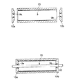
本発明の電子写真感光体の他の構成を図4及び図5を用いて説明する。図4は、本発明の電子写真感光体の他の構成の一実施例を示す断面図であり、図5は、図4の電子写真感光体の斜視図である。電子写真感光体の内側に遮光部材を設けて外部よりの光を防止する例である。図3にて説明した部材と同一の構成、機能を有するものには、同一の符号を付した。
【0031】
電子写真感光体としての感光体ドラム10は、図1にて説明した遠心重合によって成型された透明なプラスチックの円筒状基体1と、円筒状基体1の外周面に形成された導電層2と、導電層2の外周に形成された光導電性の感光体層としての有機感光体層(OPC)3と、更に感光体ドラムの外側より照射される像露光光の透過や使用される画像形成装置の機外からの光の透過を防止するため、円筒状基体1の内周面に設けられた光遮蔽部材7とにより構成される。
【0032】
遠心重合によって成型される透明なプラスチックの円筒状基体1の素材としては、上記のごとくメタクリル酸メチルエステルモノマーを用い重合したものが、透明性、強度、精度、表面性等において最も良いが、その他ポリメタクリル酸エチル、ポリメタクリル酸ブチル、ポリアクリル酸エチル、ポリアクリル酸ブチル、ポリスチレン、ポリイミド、ポリエステルあるいはポリ塩化ビニル等、又はこれらの共重合体などが使用され得る。
【0033】
導電層2としては、インジウム・スズ・酸化物(ITO)、酸化錫、酸化鉛、酸化インジウム、ヨウ化銅や、Au、Ag、Ni、Alなどからなる金属薄膜や、ITOやアルミナ導電性微粒子と樹脂とを混合した導電性樹脂が用いられ、成膜法としては、真空蒸着法、活性反応蒸着法、各種スパッタリング法、各種CVD法、浸漬塗工法、スプレー塗布法などが利用される。
【0034】
有機感光体層3は、電荷発生物質(CGM)を主成分とする電荷発生層(CGL)4と電荷輸送物質(CTM)を主成分とする電荷輸送層(CTL)5とに機能分離された二層構成の感光層とされる。二層構成の有機感光層は、CGLが薄いために像露光光の透過性が良く本発明に適する。なお有機感光体層3は、電荷発生物質(CGM)と電荷輸送物質(CTM)を1つの層中に含有する単層構成とされてもよく、該単層構成又は前記二層構成の感光層には、通常バインダー樹脂が含有される。
【0035】
前記二層構成の有機感光層を有する電子写真感光体において、CGL4に含有されるCGMとしては、LED,LD等の光源光に感光性を有するアゾ系顔料、アズレニウム顔料、フタロシアニン系顔料、ペリレン系顔料が用いられ、なかでも赤外光(700nm〜850nm)に感光するOPC感光体のCGMとしては、チタニルフタロシアニン顔料が好ましく用いられる。
【0036】
CGL4に用いられるバインダー樹脂としては、ポリビニルブチラール樹脂又はポリカーボネート樹脂が用いられ、感度、繰り返し使用時の電位変化等において優れる。これらのバインダー樹脂は、単独であるいは2種以上の混合物として用いることができる。
【0037】
CGL4の形成に用いられる溶媒あるいは分散媒としては、ケトン系又はハロゲン系溶剤が好ましく用いられ、感度、繰り返し使用時の電位変化等が更に良好となる。また、これらの溶媒は単独あるいは2種以上の混合溶媒として用いることもできる。
【0038】
CGL4中のCGMとバインダー樹脂との重量比は100:1〜1000とされ、該CGL4の膜厚は0.01〜10μmとされ、該CGL4の形成のための塗布方法としては、ブレード塗布、ワイヤーバー塗布、スプレー塗布、ディップ塗布、スライドホッパー塗布等の各塗布方法がある。
【0039】
次に前記CTL5に含有されるCTMとしては、ヒドラゾン系化合物、スチリル系化合物、ベンジジン系化合物、スチルベン系化合物等が用いられる。
【0040】
前記CTL5に用いられるバインダー樹脂としては、広範囲な絶縁性樹脂から適時選択して使用することができ、好ましい結着樹脂としては、シリコン-アルキッド樹脂、フェノール-ホルムアルデヒド樹脂、ポリ-N-ビニルカルバゾール、ポリシラン等の絶縁性樹脂を挙げることができ、これらの結着樹脂は単独あるいは2種以上混合して用いることができる。
【0041】
バインダー樹脂とCTMとの配合比は1:10〜500とされ、さらには1:20〜150が好ましい。CTL5の膜厚は1:100μmとされるが、さらに5〜50μmが好ましい。
【0042】
塗布方法としては、CGL4と同様な方法を用いることができる。
【0043】
又、有機感光体層と導電層との間に必要により中間層が設けられるが、中間層としては、例えば塩ビ酢ビ共重合体、塩ビ酢ビマレイン酸共重合体、エチルセルロース、カルボキシメチルセルロース、共重合タイプ若しくは変性タイプのアルコール可溶性ポリアミド樹脂等の0.01〜2μm厚の樹脂層とされる。
【0044】
光遮蔽部材7は機外からの光や像露光光を円筒状基体1の内部に透過しない、シート状の、例えば金属箔、プラスチック、灰色や黒色の紙またはフイルム等が用いられ、プラスチックの円筒状基体1の内壁部に、例えば透明接着剤にて貼付け接合される。
【0045】
図6は、上記図5の構成の変形例を示すもので、図1にて説明した遠心重合によって成型された透明なプラスチックの円筒状基体1と、円筒状基体1の外周面に形成された導電層2と、光導電性の感光体層としての有機感光体層(OPC)3とによて構成された電子写真感光体としての感光体ドラム10の内周面に、感光体ドラムの外側より照射される像露光光の透過や使用される画像形成装置の機外からの光の透過を防止する光遮蔽部材8を設けたものである。感光体ドラム10の内周面に、機外からの光や像露光光を円筒状基体1の内部に透過しない、シート状又は円筒状の、例えば金属箔、プラスチック、灰色や黒色の紙またはフイルム等を用いた光遮蔽部材8を挿入し、円筒状基体1の内壁部に接触又は近接して配置し、感光体ドラム10の両端に感光体ドラム10を支持する支持部材10a,10bを嵌め込み、感光体ドラム10を形成したものである。光遮蔽部材8が両端の支持部材10a,10bにて保持される。支持部材10a,10bには、感光体ドラム10が駆動回転される際の支軸20の軸受け部材であるベアリング9a,9bがそれぞれ嵌め込まれている。円筒状基体1、導電層2、有機感光体層3等の組成、構造などは、図5にて、説明したものと同様である。
【0046】
つぎに、図1〜図6にて説明した本発明の電子写真感光体を用いた画像形成装置の一実施例を図7のカラー画像形成装置を用いて説明する。図7は、本発明の電子写真感光体を用いた画像形成装置の一実施例を示すカラー画像形成装置の断面構成図である。
【0047】
静電荷像形成体としての電子写真感光体である感光体ドラム10は、透明性の高いポリメチルメタアクリル酸エステル重合体樹脂によって形成される円筒状(ドラム状)の基体の外周面に導電層、電荷発生層と電荷輸送層とからなる機能分離型有機感光体層(OPC)を形成したもので接地された状態で支軸20の回りを時計方向に駆動回転される。
【0048】
帯電手段であるスコロトロン帯電器11Y,11M,11Cおよび11Kはイエロー(Y),マゼンタ(M),シアン(C)および黒色(K)の各色の画像形成プロセスに用いられ、感光体ドラム10の前述した有機感光体層に対し所定の電位に保持されたグリッドと放電ワイヤによるコロナ放電とによって帯電作用を行い、感光体ドラム10に対し一様な電位を与える。
【0049】
像露光手段である露光光学系12Y,12M,12Cおよび12Kは、感光体ドラム10の軸方向に配列した発光素子をアレイ状に並べた線状のFL(蛍光体発光),EL(エレクトロルミネッセンス),PL(プラズマ放電),LED(発光ダイオード)や、光シャッタ機能をもつ素子を並べた線状のLISA(光磁気効果光シャッタアレイ),PLZT(透過性圧電素子シャッタアレイ),LCS(液晶シャッタ)等の露光素子と、等倍結像素子としてのセルフォックレンズとによりユニットとして構成されており、別体の画像読み取り装置によって読み取られた各色の画像信号がメモリより順次取り出されて露光光学系12Y,12M,12Cおよび12Kにそれぞれ電気信号として入力される。この実施例で使用される発光素子の発光波長は600〜900nmの範囲のものである。
【0050】
イエロー(Y),マゼンタ(M),シアン(C)および黒色(K)の一成分あるいは二成分の現像剤をそれぞれ収容する非接触現像法を用いた現像手段である現像器13Y,13M,13Cおよび13Kは、それぞれ感光体ドラム10の周面に対し所定の間隙を保って同方向に回転する現像スリーブ131Y,131M,131Cおよび131Kを備えている。
【0051】
円筒状の感光体ドラム10の外側に、感光体ドラム10を囲むように、感光体ドラム10と同心円状に円筒状の支持部材50が設けられ、円筒状の支持部材50にスコロトロン帯電器11Y,11M,11C及び11K、露光光学系12Y,12M,12C及び12K、現像器13Y,13M,13C及び13K、及びクリーニング装置19がそれぞれ取り付けられる。
【0052】
前記の現像器13Y,13M,13Cおよび13Kは、前述したスコロトロン帯電器11Y,11M,11Cおよび11Kによる帯電,露光光学系12Y,12M,12Cおよび12Kによる像露光によって形成される感光体ドラム10上の静電潜像を現像バイアス電圧の印加により非接触の状態で反転現像する。
【0053】
原稿画像は本装置とは別体の画像読み取り装置において、撮像素子により読み取られた画像あるいは、コンピュータで編集された画像を、Y,M,CおよびKの各色別の画像信号として一旦メモリに記憶し格納される。
【0054】
画像記録のスタートにより感光体駆動モータが回動して感光体ドラム10を時計方向へと回転し、同時にスコロトロン帯電器11Yの帯電作用により感光体ドラム10に電位の付与が開始される。
【0055】
感光体ドラム10は電位を付与されたあと、前記の露光光学系12Yにおいて第1の色信号すなわちイエロー(Y)の画像信号に対応する電気信号による露光が開始されドラムの回転走査によってその表面の感光層に原稿画像のイエロー(Y)の画像に対応する静電潜像を形成する。
【0056】
前記の潜像は現像器13Yにより現像スリーブ上の現像剤が非接触の状態で反転現像され感光体ドラム10の回転に応じイエロー(Y)のトナー像が形成される。
【0057】
次いで感光体ドラム10は前記イエロー(Y)のトナー像の上にさらにスコロトロン帯電器11Mの帯電作用により電位を付与され、露光光学系12Mの第2の色信号すなわちマゼンタ(M)の画像信号に対応する電気信号による露光が行われ、現像器13Mによる非接触の反転現像によって前記のイエロー(Y)のトナー像の上にマゼンタ(M)のトナー像が順次重ね合わせて形成される。
【0058】
同様のプロセスによりスコロトロン帯電器11C、露光光学系12Cおよび現像器13Cによってさらに第3の色信号に対応するシアン(C)のトナー像が、またスコロトロン帯電器11K、露光光学系12Kおよび現像器13Kによって第4の色信号に対応する黒色(K)のトナー像が順次重ね合わせて形成され、感光体ドラム10の一回転以内にその周面上にカラーのトナー像が形成される。
【0059】
かくして、感光体ドラム10の周面上に形成されたカラーのトナー像は、転写器14aにおいて、給紙カセット15より送り出され、タイミングローラ16へ搬送され、タイミングローラ16の駆動によって、感光体ドラム10上のトナー像と同期して給紙される転写材である転写紙Pに転写される。
【0060】
トナー像の転写を受けた転写紙Pは、除電器14bにおいては帯電の除去を受けてドラム周面より分離した後、搬送ベルト14eにより定着装置17へ搬送される。定着装置17において加熱・圧着されトナーを転写紙P上に溶着・定着したのち、定着装置17より排出され、排紙搬送ローラ対18aにより搬送されて排紙ローラ18を介して装置上部のトレイ上に排出される。
【0061】
一方、転写紙を分離した感光体ドラム10はクリーニング装置19においてクリーニングブレード19aによって感光体ドラム10面を摺擦され残留トナーを除去、清掃されて原稿画像のトナー像の形成を続行するかもしくは一旦停止して新たな原稿画像のトナー像の形成にかかる。クリーニングブレード19a及びクリーニングローラ19bによって掻き落とされた廃トナーは、トナー搬送スクリュウ19cによって、図示せぬ廃トナー容器へと排出される。
【0062】
上記カラープリンタでカラー画像形成を行った結果、カラートナー像の色ズレが少なく、高品質のカラー画像が得られた。
【0063】
【発明の効果】
請求項1〜4によれば、本発明により工業的に効率よく生産出来て、真円度や表面精度も良く、強度も高い電子写真感光体用の円筒状基体を提供し、且つ像露光光や機外からの光透過による画像ボケを生じることのない電子写真感光体を提供することが可能となった。
【図面の簡単な説明】
【図1】本発明の電子写真感光体の円筒状基体の製造方法の工程を示す図である。
【図2】型の一実施例を示す断面図である。
【図3】本発明の電子写真感光体の構成の一実施例を示す断面図である。
【図4】本発明の電子写真感光体の他の構成の一実施例を示す断面図である。
【図5】図4の電子写真感光体の斜視図である。
【図6】図5の構成の変形例を示す図である。
【図7】本発明の電子写真感光体を用いた画像形成装置の一実施例を示すカラー画像形成装置の断面構成図である。
【符号の説明】
1 円筒状基体
2 導電層
3 有機感光体層
4 CGL
5 CTL
6 光吸収層
7,8 光遮蔽部材
10 感光体ドラム
10a,10b 支持部材
11Y,11M,11C,11K スコロトロン帯電器
12Y,12M,12C,12K 露光光学系
13Y,13M,13C,13K 現像器
19 クリーニング装置
P 転写紙[0001]
[Industrial application fields]
The present invention relates to an electrophotographic photosensitive member used in an electrophotographic image forming apparatus such as a copying machine, a printer, and a FAX. In particular, the present invention relates to a drum-shaped electrophotographic photosensitive member.
[0002]
[Prior art]
Conventionally, as a base of a cylindrical (drum-shaped) electrophotographic photosensitive member used in an electrophotographic image forming apparatus such as a copying machine, a printer, and a FAX, a metal material such as aluminum is used to guarantee roundness and strength. There are many things that are made using.
[0003]
On the other hand, plastic is considered to be a preferable material because of its light weight and low cost, but it is not easy to manufacture a photosensitive drum with high accuracy and industrial efficiency. The major factor is that a method for easily and accurately producing a cylindrical substrate having a diameter of 30 to 200 mm with a roundness of about ± 20 μm could not be found. For this reason, conventionally, after molding a cylindrical base body, it has been necessary to ensure accuracy by cutting or polishing the surface, resulting in a decrease in productivity and an increase in cost. In addition, it has a drawback that it is weak against heat and solvent, and in addition to the accuracy of the substrate surface, there are also problems of strength and aging.
[0004]
[Problems to be solved by the invention]
As described above, an excellent cylindrical substrate using a plastic for an electrophotographic photosensitive member has been desired, but it has not been put into practical use.
[0005]
Further, when the photosensitive drum is formed of a plastic substrate, image exposure light for image formation or light from outside the apparatus is transmitted through the substrate to become miscellaneous light, and the electrostatic latent image on the photosensitive member is photostatically removed. This causes light fatigue and causes image distortion and blurring. Also, the photoconductor may cause light fatigue. In order to prevent this, if a large amount of a conductive filler or a light shielding material is added, it becomes difficult to mold the base due to a variation in viscosity, and the strength and moisture resistance are likely to deteriorate.
[0006]
The present invention provides a cylindrical substrate for an electrophotographic photosensitive member that can solve the above problems and can be industrially efficiently produced, has good roundness, high surface accuracy, and high strength, and provides image exposure light. Another object is to provide an electrophotographic photosensitive member that does not cause image blur due to light transmission from outside the apparatus.
[0007]
[Means for Solving the Problems]
The object is to inject a polymerizable liquid material into a cylindrical mold and perform polymerization by applying rotation and heat to form a transparent cylindrical substrate and a photosensitive layer provided on the outer peripheral surface of the cylindrical substrate. The electrophotographic photosensitive member is achieved by an electrophotographic photosensitive member, wherein a light absorbing layer that absorbs light having light sensitivity is provided on the inner peripheral surface of the cylindrical substrate. (First invention).
[0008]
Further, the above-mentioned object is to inject a polymerizable liquid material into a cylindrical mold and perform polymerization by applying rotation and heat to form a transparent cylindrical substrate, and a photosensitive layer provided on the outer peripheral surface of the cylindrical substrate, The electrophotographic photosensitive member comprises a light shielding member disposed in or near the inner wall portion of the cylindrical substrate (second invention).
[0009]
【Example】
A method for producing a cylindrical substrate made of a plastic material of an electrophotographic photosensitive member according to the present invention will be described with reference to FIGS. FIG. 1 is a diagram showing the steps of a method for producing a cylindrical substrate of an electrophotographic photosensitive member of the present invention, and FIG. 2 is a cross-sectional view showing an embodiment of a mold.
[0010]
First, for example, a methacrylic acid methyl ester monomer is synthesized, a catalyst is added to quickly polymerize the monomer, and then poured into a cylindrical mold, which is rotated and moderately heated to promote uniform polymerization. . After completion of the polymerization, the substrate is cooled, and the obtained substrate is taken out from the mold and cut. If necessary, a cylindrical substrate for an electrophotographic photosensitive member of an image forming apparatus is manufactured through a finishing step. FIG. 2 shows a sectional view of an example of a mold. It is a simple configuration in which a methyl methacrylate monomer liquid is poured into a cylindrical mold 101 and covers lids 102 a and 102 b, and both are fastened by bolts 103.
[0011]
The plastic cylindrical substrate produced by the above manufacturing method is a transparent substrate having a light transmittance of 90%, and has a strength comparable to aluminum, impact resistance 15 times that of glass, and a roundness of about ± 20 μm. With degree accuracy. Compared to the extrusion method, which is a molding method that is widely used at present, die scratches are not left on the surface of the cylindrical substrate. In particular, the surface is formed on a natural surface obtained by centrifugal force, and is smooth like a glass surface. A surface is formed. In addition, the strength is higher than that of the cylindrical substrate obtained by the extrusion method, and it is excellent in stable mechanical strength and heat distortion temperature without directionality, and is optimal for use in an electrophotographic photoreceptor.
[0012]
As will be described later, a photosensitive layer is provided on the outer peripheral surface of a cylindrical substrate to form an electrophotographic photosensitive member (photosensitive drum). However, the plastic substrate of the present invention is used because it is formed as a transparent substrate. Image blur occurs due to transmission of light from outside the image forming apparatus or image exposure light from the outside of the photosensitive drum. In order to prevent this, if a large amount of a light-transmitting conductive filler or light shielding material is added during molding of a plastic substrate, it becomes difficult to mold the substrate due to fluctuations in viscosity, and the strength and moisture resistance also deteriorate.
[0013]
The structure of the electrophotographic photosensitive member of the present invention will be described with reference to FIG. FIG. 3 is a sectional view showing an embodiment of the configuration of the electrophotographic photosensitive member of the present invention.
[0014]
A photosensitive drum 10 as an electrophotographic photosensitive member includes a transparent plastic cylindrical substrate 1 formed by centrifugal polymerization described in FIG. 1, a conductive layer 2 formed on the outer peripheral surface of the cylindrical substrate 1, and An organic photoreceptor layer (OPC) 3 as a photoconductive photoreceptor layer formed on the outer periphery of the conductive layer 2, and transmission of image exposure light irradiated from the outside of the photoreceptor drum and an image forming apparatus used. In order to prevent transmission of light from the outside of the machine, it is constituted by a light absorption layer 6 provided between the cylindrical substrate 1 and the conductive layer 2.
[0015]
The light absorption layer 6 absorbs light with respect to the image exposure light having photosensitivity to the organic photoreceptor layer 3, and uses a color paint that does not transmit the image exposure light, preferably a polyvinyl butyral resin or a polycarbonate resin as a binder resin, Using a black paint in which carbon black is mixed with this, the plastic cylindrical substrate 1 is formed by a coating such as a dip coating method or a spray coating method.
[0016]
As a material of the transparent plastic cylindrical substrate 1 molded by centrifugal polymerization, a polymer obtained by using a methyl methacrylate monomer as described above is the best in transparency, strength, accuracy, surface properties, etc. Polyethyl methacrylate, polybutyl methacrylate, polyethyl acrylate, polybutyl acrylate, polystyrene, polyimide, polyester, polyvinyl chloride or the like, or a copolymer thereof can be used.
[0017]
The light absorption layer 6 and the conductive layer 2 can form a combined coating film by using carbon black or the like as an opaque color material.
[0018]
As the conductive layer 2, a metal thin film made of indium / tin / oxide (ITO), tin oxide, lead oxide, indium oxide, copper iodide, Au, Ag, Ni, Al, etc., ITO or alumina conductive fine particles A conductive resin in which a resin and a resin are mixed is used. As a film forming method, a vacuum deposition method, an active reaction deposition method, various sputtering methods, various CVD methods, a dip coating method, a spray coating method, or the like is used.
[0019]
The organic photoreceptor layer 3 is functionally separated into a charge generation layer (CGL) 4 mainly composed of a charge generation material (CGM) and a charge transport layer (CTL) 5 mainly composed of a charge transport material (CTM). The photosensitive layer has a two-layer structure. Since the organic photosensitive layer having a two-layer structure has a thin CGL, the organic photosensitive layer has a good transmittance for image exposure light and is suitable for the invention. The organic photoreceptor layer 3 may have a single layer structure containing a charge generation material (CGM) and a charge transport material (CTM) in one layer, and the single layer structure or the two-layered photosensitive layer. Usually contains a binder resin.
[0020]
In the electrophotographic photosensitive member having the organic photosensitive layer having the two-layer structure, CGM contained in CGL4 may be an azo pigment, an azulenium pigment, a phthalocyanine pigment, or a perylene-based pigment that is sensitive to light from a light source such as an LED or LD. In particular, a titanyl phthalocyanine pigment is preferably used as the CGM of the OPC photoreceptor that is sensitive to infrared light (700 nm to 850 nm).
[0021]
As the binder resin used for CGL4, polyvinyl butyral resin or polycarbonate resin is used, which is excellent in sensitivity, potential change during repeated use, and the like. These binder resins can be used alone or as a mixture of two or more.
[0022]
As the solvent or dispersion medium used for forming CGL4, a ketone or halogen solvent is preferably used, and sensitivity, potential change during repeated use, and the like are further improved. These solvents can be used alone or as a mixed solvent of two or more.
[0023]
The weight ratio of CGM and binder resin in CGL4 is set to 100: 1 to 1000, and the film thickness of CGL4 is set to 0.01 to 10 μm. The coating method for forming CGL4 includes blade coating and wire bar coating. There are various coating methods such as spray coating, dip coating, and slide hopper coating.
[0024]
Next, as CTM contained in CTL5, hydrazone compounds, styryl compounds, benzidine compounds, stilbene compounds, and the like are used.
[0025]
The binder resin used in the CTL 5 can be selected from a wide range of insulating resins in a timely manner. Preferred binder resins include silicon-alkyd resin, phenol-formaldehyde resin, poly-N-vinylcarbazole, An insulating resin such as polysilane can be used, and these binder resins can be used alone or in combination of two or more.
[0026]
The compounding ratio of the binder resin and CTM is 1:10 to 500, and more preferably 1:20 to 150. The film thickness of CTL5 is set to 1: 100 μm, and more preferably 5 to 50 μm.
[0027]
As a coating method, a method similar to CGL4 can be used.
[0028]
An intermediate layer is provided between the organic photoreceptor layer and the conductive layer as necessary. Examples of the intermediate layer include a vinyl acetate vinyl acetate copolymer, a vinyl acetate vinyl maleic acid copolymer, ethyl cellulose, carboxymethyl cellulose, and copolymer. The resin layer has a thickness of 0.01 to 2 μm, such as a type or modified type alcohol-soluble polyamide resin.
[0029]
In the above embodiment, the light absorbing layer 6 is provided on the outer peripheral surface of the cylindrical substrate 1. However, the transparent plastic cylindrical substrate of the present invention has less internal stress and has uneven light refraction when transmitting light. It is also possible to provide the light absorption layer 6 on the inner peripheral surface of the cylindrical substrate 1.
[0030]
Another structure of the electrophotographic photosensitive member of the present invention will be described with reference to FIGS. FIG. 4 is a cross-sectional view showing an embodiment of another configuration of the electrophotographic photosensitive member of the present invention, and FIG. 5 is a perspective view of the electrophotographic photosensitive member of FIG. In this example, a light shielding member is provided inside the electrophotographic photosensitive member to prevent light from the outside. Components having the same configuration and function as those described in FIG. 3 are denoted by the same reference numerals.
[0031]
A photosensitive drum 10 as an electrophotographic photosensitive member includes a transparent plastic cylindrical substrate 1 formed by centrifugal polymerization described in FIG. 1, a conductive layer 2 formed on the outer peripheral surface of the cylindrical substrate 1, and An organic photoreceptor layer (OPC) 3 as a photoconductive photoreceptor layer formed on the outer periphery of the conductive layer 2, and transmission of image exposure light irradiated from the outside of the photoreceptor drum and an image forming apparatus used. In order to prevent the transmission of light from outside the machine, it is constituted by a light shielding member 7 provided on the inner peripheral surface of the cylindrical substrate 1.
[0032]
As a material of the transparent plastic cylindrical substrate 1 molded by centrifugal polymerization, a polymer obtained by using a methyl methacrylate monomer as described above is the best in transparency, strength, accuracy, surface properties, etc. Polyethyl methacrylate, polybutyl methacrylate, polyethyl acrylate, polybutyl acrylate, polystyrene, polyimide, polyester, polyvinyl chloride or the like, or a copolymer thereof can be used.
[0033]
As the conductive layer 2, a metal thin film made of indium / tin / oxide (ITO), tin oxide, lead oxide, indium oxide, copper iodide, Au, Ag, Ni, Al, etc., ITO or alumina conductive fine particles A conductive resin in which a resin and a resin are mixed is used. As a film forming method, a vacuum deposition method, an active reaction deposition method, various sputtering methods, various CVD methods, a dip coating method, a spray coating method, or the like is used.
[0034]
The organic photoreceptor layer 3 is functionally separated into a charge generation layer (CGL) 4 mainly composed of a charge generation material (CGM) and a charge transport layer (CTL) 5 mainly composed of a charge transport material (CTM). The photosensitive layer has a two-layer structure. Since the organic photosensitive layer having a two-layer structure has a thin CGL, the organic photosensitive layer has a good transmittance for image exposure light and is suitable for the invention. The organic photoreceptor layer 3 may have a single layer structure containing a charge generation material (CGM) and a charge transport material (CTM) in one layer, and the single layer structure or the two-layered photosensitive layer. Usually contains a binder resin.
[0035]
In the electrophotographic photosensitive member having the organic photosensitive layer having the two-layer structure, CGM contained in CGL4 may be an azo pigment, an azulenium pigment, a phthalocyanine pigment, or a perylene-based pigment that is sensitive to light from a light source such as an LED or LD. In particular, a titanyl phthalocyanine pigment is preferably used as the CGM of the OPC photoreceptor that is sensitive to infrared light (700 nm to 850 nm).
[0036]
As the binder resin used for CGL4, polyvinyl butyral resin or polycarbonate resin is used, which is excellent in sensitivity, potential change during repeated use, and the like. These binder resins can be used alone or as a mixture of two or more.
[0037]
As the solvent or dispersion medium used for forming CGL4, a ketone or halogen solvent is preferably used, and sensitivity, potential change during repeated use, and the like are further improved. These solvents can be used alone or as a mixed solvent of two or more.
[0038]
The weight ratio of CGM and binder resin in CGL4 is set to 100: 1 to 1000, and the film thickness of CGL4 is set to 0.01 to 10 μm. The coating method for forming CGL4 includes blade coating and wire bar coating. There are various coating methods such as spray coating, dip coating, and slide hopper coating.
[0039]
Next, as CTM contained in CTL5, hydrazone compounds, styryl compounds, benzidine compounds, stilbene compounds, and the like are used.
[0040]
The binder resin used in the CTL 5 can be selected from a wide range of insulating resins in a timely manner. Preferred binder resins include silicon-alkyd resin, phenol-formaldehyde resin, poly-N-vinylcarbazole, An insulating resin such as polysilane can be used, and these binder resins can be used alone or in combination of two or more.
[0041]
The compounding ratio of the binder resin and CTM is 1:10 to 500, and more preferably 1:20 to 150. The film thickness of CTL5 is set to 1: 100 μm, and more preferably 5 to 50 μm.
[0042]
As a coating method, a method similar to CGL4 can be used.
[0043]
An intermediate layer is provided between the organic photoreceptor layer and the conductive layer as necessary. Examples of the intermediate layer include a vinyl acetate vinyl acetate copolymer, a vinyl acetate vinyl maleic acid copolymer, ethyl cellulose, carboxymethyl cellulose, and copolymer. The resin layer has a thickness of 0.01 to 2 μm, such as a type or modified type alcohol-soluble polyamide resin.
[0044]
The light shielding member 7 is made of sheet-like material such as metal foil, plastic, gray or black paper or film, which does not transmit light from outside the apparatus or image exposure light into the inside of the cylindrical substrate 1, and is a plastic cylinder. For example, a transparent adhesive is attached to and bonded to the inner wall portion of the substrate 1.
[0045]
FIG. 6 shows a modification of the configuration shown in FIG. 5, and is formed on the transparent plastic cylindrical base 1 molded by centrifugal polymerization described in FIG. 1 and the outer peripheral surface of the cylindrical base 1. On the inner peripheral surface of the photosensitive drum 10 as an electrophotographic photosensitive member constituted by the conductive layer 2 and the organic photosensitive layer (OPC) 3 as a photoconductive photosensitive layer, the outer side of the photosensitive drum. A light shielding member 8 for preventing transmission of image exposure light irradiated more and light from outside the image forming apparatus used is provided. On the inner peripheral surface of the photosensitive drum 10, sheet-like or cylindrical, for example, metal foil, plastic, gray or black paper or film that does not transmit light or image exposure light from outside the apparatus to the inside of the cylindrical substrate 1. Is inserted in contact with or in close proximity to the inner wall of the cylindrical substrate 1, and support members 10a and 10b for supporting the photosensitive drum 10 are fitted into both ends of the photosensitive drum 10, The photosensitive drum 10 is formed. The light shielding member 8 is held by the support members 10a and 10b at both ends. Bearings 9a and 9b, which are bearing members of the support shaft 20 when the photosensitive drum 10 is driven and rotated, are fitted into the support members 10a and 10b, respectively. The composition, structure, etc. of the cylindrical substrate 1, the conductive layer 2, the organic photoreceptor layer 3, etc. are the same as those described with reference to FIG.
[0046]
Next, an example of an image forming apparatus using the electrophotographic photosensitive member of the present invention described with reference to FIGS. 1 to 6 will be described using the color image forming apparatus of FIG. FIG. 7 is a cross-sectional configuration diagram of a color image forming apparatus showing an embodiment of an image forming apparatus using the electrophotographic photosensitive member of the present invention.
[0047]
A photosensitive drum 10 which is an electrophotographic photosensitive member as an electrostatic charge image forming body has a conductive layer on the outer peripheral surface of a cylindrical (drum-shaped) substrate formed of a highly transparent polymethylmethacrylate polymer resin. A function-separated organic photoreceptor layer (OPC) composed of a charge generation layer and a charge transport layer is formed, and is driven to rotate clockwise around the spindle 20 while being grounded.
[0048]
The scorotron chargers 11Y, 11M, 11C, and 11K as charging means are used in the image forming process of each color of yellow (Y), magenta (M), cyan (C), and black (K). The organic photoreceptor layer is charged by a grid held at a predetermined potential and corona discharge by a discharge wire, and a uniform potential is applied to the photoreceptor drum 10.
[0049]
The exposure optical systems 12Y, 12M, 12C and 12K as image exposure means are linear FL (phosphor light emission), EL (electroluminescence) in which light emitting elements arranged in the axial direction of the photosensitive drum 10 are arranged in an array. , PL (plasma discharge), LED (light emitting diode), linear LISA (magneto-optical shutter array) with elements having an optical shutter function, PLZT (transparent piezoelectric shutter array), LCS (liquid crystal shutter) ) Etc. and a SELFOC lens as a unity magnification imaging element as a unit, and the image signal of each color read by a separate image reading device is sequentially taken out from the memory, and the exposure optical system 12Y, 12M, 12C and 12K are inputted as electric signals, respectively. The light emitting wavelength of the light emitting element used in this example is in the range of 600 to 900 nm.
[0050]
Developing units 13Y, 13M, and 13C, which are developing units using a non-contact developing method that respectively contain one-component or two-component developers of yellow (Y), magenta (M), cyan (C), and black (K). And 13K include developing sleeves 131Y, 131M, 131C, and 131K that rotate in the same direction with a predetermined gap with respect to the peripheral surface of the photosensitive drum 10, respectively.
[0051]
A cylindrical support member 50 concentrically with the photoconductive drum 10 is provided outside the cylindrical photoconductive drum 10 so as to surround the photoconductive drum 10, and the scorotron charger 11Y, 11M, 11C and 11K, exposure optical systems 12Y, 12M, 12C and 12K, developing devices 13Y, 13M, 13C and 13K, and a cleaning device 19 are attached, respectively.
[0052]
The developing units 13Y, 13M, 13C and 13K are formed on the photosensitive drum 10 formed by the above-described charging by the scorotron charging units 11Y, 11M, 11C and 11K and image exposure by the exposure optical systems 12Y, 12M, 12C and 12K. The electrostatic latent image is reversely developed in a non-contact state by applying a developing bias voltage.
[0053]
The document image is stored in the memory once as an image signal for each color of Y, M, C, and K by an image reading device separate from the present device, and an image read by the image sensor or an image edited by a computer. Stored.
[0054]
At the start of image recording, the photosensitive member driving motor rotates to rotate the photosensitive drum 10 clockwise, and at the same time, application of a potential to the photosensitive drum 10 is started by the charging action of the scorotron charger 11Y.
[0055]
After the photosensitive drum 10 is applied with an electric potential, exposure by the electric signal corresponding to the first color signal, that is, the yellow (Y) image signal is started in the exposure optical system 12Y. An electrostatic latent image corresponding to the yellow (Y) image of the original image is formed on the photosensitive layer.
[0056]
The latent image is reversed and developed by the developing device 13Y in a state where the developer on the developing sleeve is not in contact, and a yellow (Y) toner image is formed in accordance with the rotation of the photosensitive drum 10.
[0057]
Next, the photosensitive drum 10 is further applied with a potential on the yellow (Y) toner image by the charging action of the scorotron charger 11M, so that the second color signal of the exposure optical system 12M, that is, the magenta (M) image signal. Exposure is performed with a corresponding electrical signal, and a magenta (M) toner image is sequentially superimposed on the yellow (Y) toner image by non-contact reversal development by the developing unit 13M.
[0058]
By the same process, a cyan (C) toner image corresponding to the third color signal is obtained by the scorotron charger 11C, the exposure optical system 12C and the developing device 13C, and the scorotron charger 11K, the exposure optical system 12K and the developing device 13K. As a result, a black (K) toner image corresponding to the fourth color signal is sequentially superimposed and formed, and a color toner image is formed on the peripheral surface within one rotation of the photosensitive drum 10.
[0059]
Thus, the color toner image formed on the peripheral surface of the photosensitive drum 10 is sent out from the paper feed cassette 15 in the transfer unit 14a, conveyed to the timing roller 16, and driven by the timing roller 16, thereby the photosensitive drum. 10 is transferred to transfer paper P, which is a transfer material fed in synchronism with the toner image on 10.
[0060]
The transfer paper P that has received the toner image transfer is subjected to charge removal in the static eliminator 14b and separated from the drum peripheral surface, and is then conveyed to the fixing device 17 by the conveyance belt 14e. After the toner is fused and fixed on the transfer paper P by being heated and pressed in the fixing device 17, the toner is discharged from the fixing device 17, transported by the paper discharge roller pair 18 a, and then on the tray above the device via the paper discharge roller 18. To be discharged.
[0061]
On the other hand, the photosensitive drum 10 from which the transfer paper has been separated is rubbed against the surface of the photosensitive drum 10 by a cleaning blade 19a in the cleaning device 19 to remove residual toner and cleaned to continue forming a toner image of the original image or temporarily. It stops and starts forming a new original toner image. Waste toner scraped off by the cleaning blade 19a and the cleaning roller 19b is discharged to a waste toner container (not shown) by the toner conveying screw 19c.
[0062]
As a result of forming a color image with the color printer, a color image of the color toner image was little and a high quality color image was obtained.
[0063]
【The invention's effect】
According to the first to fourth aspects, the present invention provides a cylindrical substrate for an electrophotographic photosensitive member that can be produced industrially efficiently by the present invention, has good roundness, surface accuracy, and high strength, and image exposure light. In addition, it is possible to provide an electrophotographic photosensitive member that does not cause image blur due to light transmission from outside the apparatus.
[Brief description of the drawings]
FIG. 1 is a diagram showing the steps of a method for producing a cylindrical substrate of an electrophotographic photosensitive member according to the present invention.
FIG. 2 is a cross-sectional view showing an embodiment of a mold.
FIG. 3 is a cross-sectional view showing an example of the configuration of the electrophotographic photosensitive member of the present invention.
FIG. 4 is a cross-sectional view showing an example of another configuration of the electrophotographic photosensitive member of the present invention.
5 is a perspective view of the electrophotographic photosensitive member of FIG. 4. FIG.
6 is a diagram showing a modification of the configuration of FIG.
FIG. 7 is a cross-sectional configuration diagram of a color image forming apparatus showing an embodiment of an image forming apparatus using the electrophotographic photosensitive member of the present invention.
[Explanation of symbols]
DESCRIPTION OF SYMBOLS 1 Cylindrical base | substrate 2 Conductive layer 3 Organic photoreceptor layer 4 CGL
5 CTL
6 Light absorbing layer 7, 8 Light shielding member 10 Photosensitive drums 10a, 10b Support members 11Y, 11M, 11C, 11K Scorotron chargers 12Y, 12M, 12C, 12K Exposure optical systems 13Y, 13M, 13C, 13K Developer 19 Cleaning Device P Transfer paper