JP3836322B2 - Use of ECC / parity bits to store predecode information - Google Patents
Use of ECC / parity bits to store predecode information Download PDFInfo
- Publication number
- JP3836322B2 JP3836322B2 JP2000556301A JP2000556301A JP3836322B2 JP 3836322 B2 JP3836322 B2 JP 3836322B2 JP 2000556301 A JP2000556301 A JP 2000556301A JP 2000556301 A JP2000556301 A JP 2000556301A JP 3836322 B2 JP3836322 B2 JP 3836322B2
- Authority
- JP
- Japan
- Prior art keywords
- cache
- instruction
- predecode
- level
- information
- Prior art date
- Legal status (The legal status is an assumption and is not a legal conclusion. Google has not performed a legal analysis and makes no representation as to the accuracy of the status listed.)
- Expired - Lifetime
Links
Images


Classifications
-
- G—PHYSICS
- G06—COMPUTING; CALCULATING OR COUNTING
- G06F—ELECTRIC DIGITAL DATA PROCESSING
- G06F9/00—Arrangements for program control, e.g. control units
- G06F9/06—Arrangements for program control, e.g. control units using stored programs, i.e. using an internal store of processing equipment to receive or retain programs
- G06F9/30—Arrangements for executing machine instructions, e.g. instruction decode
- G06F9/38—Concurrent instruction execution, e.g. pipeline, look ahead
- G06F9/3818—Decoding for concurrent execution
- G06F9/382—Pipelined decoding, e.g. using predecoding
-
- G—PHYSICS
- G06—COMPUTING; CALCULATING OR COUNTING
- G06F—ELECTRIC DIGITAL DATA PROCESSING
- G06F12/00—Accessing, addressing or allocating within memory systems or architectures
- G06F12/02—Addressing or allocation; Relocation
- G06F12/08—Addressing or allocation; Relocation in hierarchically structured memory systems, e.g. virtual memory systems
- G06F12/0802—Addressing of a memory level in which the access to the desired data or data block requires associative addressing means, e.g. caches
- G06F12/0875—Addressing of a memory level in which the access to the desired data or data block requires associative addressing means, e.g. caches with dedicated cache, e.g. instruction or stack
-
- G—PHYSICS
- G06—COMPUTING; CALCULATING OR COUNTING
- G06F—ELECTRIC DIGITAL DATA PROCESSING
- G06F12/00—Accessing, addressing or allocating within memory systems or architectures
- G06F12/02—Addressing or allocation; Relocation
- G06F12/08—Addressing or allocation; Relocation in hierarchically structured memory systems, e.g. virtual memory systems
- G06F12/0802—Addressing of a memory level in which the access to the desired data or data block requires associative addressing means, e.g. caches
- G06F12/0893—Caches characterised by their organisation or structure
- G06F12/0897—Caches characterised by their organisation or structure with two or more cache hierarchy levels
-
- G—PHYSICS
- G06—COMPUTING; CALCULATING OR COUNTING
- G06F—ELECTRIC DIGITAL DATA PROCESSING
- G06F9/00—Arrangements for program control, e.g. control units
- G06F9/06—Arrangements for program control, e.g. control units using stored programs, i.e. using an internal store of processing equipment to receive or retain programs
- G06F9/30—Arrangements for executing machine instructions, e.g. instruction decode
- G06F9/30145—Instruction analysis, e.g. decoding, instruction word fields
- G06F9/30149—Instruction analysis, e.g. decoding, instruction word fields of variable length instructions
- G06F9/30152—Determining start or end of instruction; determining instruction length
-
- G—PHYSICS
- G06—COMPUTING; CALCULATING OR COUNTING
- G06F—ELECTRIC DIGITAL DATA PROCESSING
- G06F9/00—Arrangements for program control, e.g. control units
- G06F9/06—Arrangements for program control, e.g. control units using stored programs, i.e. using an internal store of processing equipment to receive or retain programs
- G06F9/30—Arrangements for executing machine instructions, e.g. instruction decode
- G06F9/38—Concurrent instruction execution, e.g. pipeline, look ahead
- G06F9/3802—Instruction prefetching
- G06F9/3816—Instruction alignment, e.g. cache line crossing
Description
【0001】
【発明の背景】
1.技術分野
この発明は、マイクロプロセッサに関し、より特定的には、マイクロプロセッサ内の可変長命令をデコードすることに関する。
【0002】
2.背景技術
x86命令セットのために書かれたソフトウェアアプリケーションの数は、かなり多い。その結果、より新しくより進歩した命令セットの導入にもかかわらず、マイクロプロセッサの設計者は、x86命令セットを実行することのできるマイクロプロセッサを設計し続けてきた。
【0003】
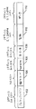
x86命令セットは、比較的複雑であり、複数個の可変長命令を特徴とする。x86命令セットを示す一般的なフォーマットを図1に示す。図に例示されるように、x86命令は、1から5のオプションのプレフィックスバイト102と、その後に続く操作コード(opコード)フィールド104と、オプションのアドレッシングモード(Mod R/M)バイト106と、オプションのスケール−インデックス−ベース(SIB)バイト108と、オプションの変位フィールド110と、オプションの即値データフィールド112とからなる。
【0004】
操作コードフィールド104は、特定の命令のための基本操作を定義する。特定の操作コードのデフォルト操作は、1つ以上のプレフィックスバイト102によって変更可能である。たとえば、プレフィックスバイト102の1つを用いて、命令についてのアドレスまたはオペランドサイズを変更し、メモリアドレッシングに用いられるデフォルトセグメントを無効にし、または複数回ストリング操作を繰返すようプロセッサに命令することが可能である。操作コードフィールド104は、もし存在するならばプレフィックスバイト102の後に続き、1または2バイトの長さであってもよい。アドレッシングモード(Mod R/M)バイト106は、使用されるレジスタおよびメモリアドレッシングモードを特定する。スケール−インデックス−ベース(SIB)バイト108は、スケールファクタおよびインデックスファクタを用いる32ビットベース相対アドレッシングにおいてのみ用いられる。SIBバイト108内のベースフィールドは、どのレジスタがアドレス計算のためのベース値を含むかを特定し、SIBバイト108内のインデックスフィールドは、どのレジスタがインデックス値を含むかを特定する。SIBバイト108内のスケールフィールドは、任意の変位とともにベース値に加算されるより前に、インデックス値に乗算される2のべきを特定する。次の命令フィールドは、変位フィールド110であり、これはオプションであり、1から4バイトの長さであってもよい。変位フィールド110は、アドレス計算に用いられる定数を含む。オプションの即値フィールド112は、これもまた1から4バイトの長さであってもよいが、命令オペランドとして用いられる定数を含む。最短のx86命令は、1バイトのみの長さであり、単一の操作コードバイトを含む。80286は、命令の最大長を10バイトに設定し、80386および80486はどちらも、最大15バイトの命令長を可能にする。
【0005】
x86命令セットの複雑性は、高性能のx86互換のマイクロプロセッサを実現する際に多くの困難を提起する。特に、x86命令の可変長は、命令のデコードを困難にする。命令のデコードは典型的には、命令の境界を決定し、次に命令内の各フィールド、たとえば操作コードフィールドおよびオペランドフィールドを特定することを伴なう。デコードは典型的には、命令が実行されるより前に命令キャッシュからフェッチされるときに起こる。
【0006】
命令の境界を決定するためのある方法は、主メモリから読出され命令キャッシュに記憶される際に各命令バイトについて1つ以上のプリデコードビットを生成しかつ記憶することを伴なう。プリデコードビットは、それが関連付けられる命令バイトについての情報を与える。たとえば、アサートされたプリデコード開始ビットは、関連付けられた命令バイトが命令の第1のバイトであることを示す。特定の命令バイトについての開始ビットが一旦計算されると、それは命令バイトとともに命令キャッシュ内に記憶される。「フェッチ」が実行されるとき、多数の命令バイトが命令キャッシュから読出され、実行のための準備としてデコードされる。関連付けられた開始ビットはいずれも、フェッチとともに個々の命令のための有効マスクを生成するためにスキャンされる。有効マスクは、各ビットが特定の命令バイトに対応している一連のビットである。命令の第1のバイト、命令の最終バイト、および命令の第1のバイトと最終バイトとの間にあるすべてのバイトに関連付けられる有効マスクビットがアサートされる。すべての他の有効マスクビットは、アサートされない。有効マスクが計算されると、それを用いて他の命令からのバイトをマスク消去(mask-off)可能である。
【0007】
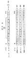
図2を次に参照すると、例示の有効マスクが示される。図は、フェッチ120の一部と、その関連付けられた開始ビット122とを示す。命令B128のための有効マスク126が生成されるべきであると想定すると、開始ビット122Aと、開始ビット122Bとの間のすべてのビットがアサートされてマスク126を生成する。一旦生成されると次に、有効マスク126を用いて、命令B128の一部ではないフェッチ120内のすべてのバイトをマスク消去可能である。
【0008】
上の記載が示すように、プリデコード情報は、デコード回数を低減するために特に有用であるだろう。命令キャッシュ内に命令バイトとともにプリデコード情報を記憶することによって、対応する命令が複数回(たとえばループで)実行されたとしても、プリデコード情報は1回計算されるだけで済む。しかし、残念ながら、命令が置換されるかまたは命令キャッシュから廃棄されるとき、関連付けられたプリデコード情報はいずれも失われる。次に命令が命令キャッシュに読出されるときに、プリデコード情報はまたもや生成されなければならない。プリデコード情報が計算されるのを待つことによって生じる時間遅延は、分岐予測誤りまたはキャッシュミスの結果として命令が命令キャッシュに読出されるとき特に性能を損なう可能性がある。必要とされるより前に投機的にプリフェッチされる命令とは対照的に、分岐予測誤りまたはキャッシュミスによって生じるフェッチは、要求された命令を受取るのを待つ間にマイクロプロセッサのデコーダおよび機能ユニットをストールさせてしまう可能性がある。この場合には、プリデコード情報を発生するために必要とされる時間は、マイクロプロセッサの性能にかなりの影響を与え兼ねない。
【0009】
これらおよび他の理由のために、プリデコード回数を低減するための方法および装置が所望される。特に、命令キャッシュから先に廃棄されてしまった命令についてのプリデコード情報を生成するために必要とされる時間を減ずるための方法および装置が所望される。
【0010】
【発明の開示】
以上に概略した課題は、レベル2キャッシュにプリデコード情報を記憶することのできるマイクロプロセッサによって大部分解決される。ある実施例では、マイクロプロセッサは、プリデコード情報または対応する命令バイトのいずれかが命令キャッシュ内で置換されるときレベル2キャッシュ内にプリデコード情報を記憶するよう構成可能である。
【0011】
ある実施例では、マイクロプロセッサは、プリデコードユニットおよび命令キャッシュを含む。プリデコードユニットは、レベル2キャッシュから命令バイトを受取り対応するプリデコード情報を生成するよう構成される。命令キャッシュは、プリデコードユニットに結合され、2つの複数個の記憶場所:命令バイトを記憶するためのものと、命令バイトに対応するプリデコード情報を記憶するための第2のものとを含む。命令キャッシュは、命令バイトを受取り記憶しかつプリデコードユニットからの情報をプリデコードするよう構成可能である。命令キャッシュはまた、命令バイトおよび対応するプリデコード情報が命令キャッシュ内で置換されるとき対応するプリデコード情報の少なくとも一部を出力するよう構成可能である。プリデコード情報は出力されレベル2キャッシュ内に記憶され得る。命令キャッシュ内で置換された後およびレベル2キャッシュ内で置換されるより前に同じ命令バイトが必要とされる場合、命令バイトおよび命令に付随するプリデコード情報は、レベル2キャッシュから取出し可能である。有利なことには、命令バイトをプリデコードすることの遅延は、いくつかの場合においては回避可能である。
【0012】
別の実施例では、プリデコード情報は、パリティおよびまたはエラーチェックおよび訂正情報を記憶するよう構成されるレベル2キャッシュ内の記憶場所に記憶され得る。パリティおよびまたはエラーチェックおよび訂正記憶場所を用いることによって、レベル2キャッシュ構成への変更を低減したり排除したりすることが可能である。
【0013】
さらに別の実施例では、無効定数が、有効プリデコード情報をまだ有していない命令バイトのためにレベル2キャッシュ内に記憶され得る。プリデコードユニットは、レベル2キャッシュから命令バイトを読出すときに無効定数を検出し、これに応答して新しいプリデコード情報を計算するよう構成され得る。
【0014】
可変長命令をプリデコードするための方法もまた企図される。ある実施例では、この方法は、主システムメモリから命令バイトを読出し、命令バイトに対応するプリデコード情報を生成するステップを含む。命令バイトおよびプリデコード情報は、命令キャッシュ内に記憶される。プリデコード情報に対応する命令バイトが命令キャッシュ内で上書きされるとき、プリデコード情報の少なくとも一部がレベル2キャッシュに出力され記憶される。プリデコード情報はやはり、パリティおよびまたはエラーチェックおよび訂正データを記憶するよう構成されるレベル2キャッシュ内の記憶場所内に記憶され得る。
【0015】
プリデコードデータを記憶するよう構成されるコンピュータシステムもまた企図される。ある実施例では、コンピュータシステムは、レベル2キャッシュおよびマイクロプロセッサを含んでもよい。マイクロプロセッサは、レベル2キャッシュに結合されてもよく、上述したようにプリデコードユニットおよび命令キャッシュで構成されてもよい。プリデコードユニットは、レベル2キャッシュから命令バイトを受取り対応するプリデコード情報を生成するよう構成されてもよい。命令キャッシュは、プリデコードユニットに結合されてもよく、前記命令バイトが置換されたときその記憶されたプリデコード情報の少なくとも一部を出力してレベル2キャッシュ中に記憶するように構成されてもよい。レベル2キャッシュは、パリティおよびまたはエラーチェックおよび制御データを記憶するよう構成される記憶場所内に命令キャッシュからのプリデコード情報を記憶するよう構成されてもよい。
【0016】
この発明の他の目的および利点は、以下の詳細な記載を読みかつ添付の図面を参照すると明らかとなるであろう。
【0017】
この発明は、さまざまな変形および代替の態様を受入れるが、その具体的な実施例は、図面に例として示され、ここに詳細に記載される。しかしながら、図面およびその詳細な記載は、開示される特定の態様にこの発明を限定するものではなく、反対に、その意図は、前掲の特許請求の範囲によって定義されるようなこの発明の範囲内にあるすべての変形、等価および代替を含むものであることが理解されるべきである。
【0018】
【発明を実施するモード】
ここで図3を参照すると、マイクロプロセッサ10のある実施例のブロック図が示される。マイクロプロセッサ10は、プリフェッチ/プリデコードユニット12と、分岐予測ユニット14と、命令キャッシュ16と、命令整列ユニット18と、複数個のデコードユニット20A〜20Cと、複数個のリザベーションステーション22A〜22Cと、複数個の機能ユニット24A〜24Cと、ロード/ストアユニット26と、データキャッシュ28と、レジスタファイル30と、リオーダバッファ32と、MROMユニット34とを含む。特定の参照番号が文字の後に付されているここに参照される要素は、参照番号のみによって集合的に参照されることがある。たとえば、リザベーションステーション22A〜22Cは、リザベーションステーション22として集合的に参照されることがある。
【0019】
プリフェッチ/プリデコードユニット12は、主メモリサブシステム(図示せず)からの命令を受取るよう結合され、さらに命令キャッシュ16および分岐予測ユニット14に結合される。同様に、分岐予測ユニット14は、命令キャッシュ16に結合される。分岐予測ユニット14はまた、命令整列ユニット18および機能ユニット24A〜Cに結合される。命令キャッシュ16はさらに、MROMユニット34および命令整列ユニット18に結合される。命令整列ユニット18は、ロード/ストアユニット26におよびそれぞれのデコードユニット20A〜Cに結合される。それぞれのデコードユニット20A〜Cは、リザベーションステーション22A〜Cに結合され、これはさらにそれぞれの機能ユニット24A〜Cに結合される。加えて、命令整列ユニット18およびリザベーションステーション22は、レジスタファイル30およびリオーダバッファ32に結合される。機能ユニット24は、ロード/ストアユニット26、レジスタファイル30およびリオーダバッファ30にも結合される。データキャッシュ28は、ロード/ストアユニット26におよび主メモリサブシステムに結合される。最後に、MROMユニット34は、命令整列ユニット18に結合される。
【0020】
命令は、プリフェッチ/プリデコードユニット12によって主メモリからプリフェッチされる。プリフェッチ/プリデコードユニット12は、可変長命令を固定長命令にプリデコードし、これは次に命令キャッシュ16内に記憶される。命令は、それらが実際にプリフェッチ方式を用いることによって要求されるより前にプリフェッチおよびプリデコード可能である。さまざまなプリフェッチ方式が、プリフェッチ/プリデコードユニット12によって採用可能である。プリデコードユニット12および命令キャッシュ16のさらに詳細な記載に進む前に、図に示される例示のマイクロプロセッサ10の実施例に関する一般的な局面を記載する。
【0021】
マイクロプロセッサ10は、条件付き分岐命令の後の命令を投機的にフェッチするために分岐予測を採用し得る。分岐予測ユニット14は、分岐予測操作を実行するために含まれる。ある実施例では、最大2つの分岐ターゲットアドレスが、命令キャッシュ16中に各キャッシュラインの各16バイト部分ごとに記憶される。プリフェッチ/プリデコードユニット12は、特定のラインがプリデコードされると最初の分岐ターゲットを決定する。キャッシュラインに対応する分岐ターゲットに対するその後の更新は、キャッシュライン内の命令の実行によって起こり得る。命令キャッシュ16は、分岐予測ユニット14にフェッチされるべき命令アドレスの表示を与える。これは、分岐予測ユニット14が分岐予測を形成するときにどの分岐ターゲットアドレスを選択すべきかを決定することを可能にする。命令整列ユニット18および機能ユニット24は、分岐予測ユニット14に更新情報を与える。分岐予測ユニット14は、キャッシュラインの16バイト部分当り2個のターゲットを記憶するので、ライン内のいくつかの分岐命令についての予測は、分岐予測ユニット14中に記憶されないかもしれない。命令整列ユニット18は、分岐予測ユニット14によって予測されなかった分岐命令を検出するよう構成され得る。機能ユニット24は、分岐命令を実行し、予測された分岐方向が予測誤りでなかったかどうかを決定する。分岐方向は、その後の命令が分岐命令のターゲットアドレスからフェッチされる場合には「テイクン」であり得る。反対に、分岐方向は、その後の命令が分岐命令に連続するメモリ場所からフェッチされる場合には「ノットテイクン」であり得る。予測誤りされた分岐命令が検出されると、予測誤りされた分岐の後に続く命令は、マイクロプロセッサ10のさまざまなユニットから廃棄される。さまざまな好適な分岐予測アルゴリズムが、分岐予測ユニット14によって採用可能である。
【0022】
命令キャッシュ16は、プリフェッチ/プリデコードユニット12から受取られた命令を記憶するために設けられる高速キャッシュメモリである。記憶された命令は次に、命令キャッシュ16からフェッチされ、命令整列ユニット18に転送される。ある実施例では、命令キャッシュ16は、セットアソシアティブ構造として構成可能である。命令キャッシュ16は加えて、アクセス時間を早めるためにウェイ予測方式を採用してよい。たとえば、命令の各ラインを識別するタグにアクセスしタグをフェッチアドレスと比較してウェイを選択する代わりに、命令キャッシュ16は、アクセスされるウェイを予測し得る。この態様では、ウェイは、アレイにアクセスするより前に投機的に選択される。ウェイ予測を用いて、命令キャッシュ16のアクセス時間は、ダイレクトマッピングされたキャッシュと同様になり得る。命令バイトが読出された後、ベリフィケーションのためにタグ比較が実行される。ウェイ予測が正しくなければ、正しい命令バイトがフェッチされ、正しくない命令バイト(処理パイプラインのさらに下方にある)は、廃棄される。なお、命令キャッシュ16は、フルアソシアティブ構成、セットアソシアティブ構成またはダイレクトマップド構成で実現可能である。
【0023】
MROMユニット34は、「高速パス命令」のシーケンスを記憶するよう構成されるリードオンリメモリである。高速パス命令は、デコーダ20A〜Cおよび機能ユニット24A〜Cによってデコードおよび実行され得る命令である。対照的に、「MROM命令」は、デコーダ20A〜Cおよび機能ユニット24A〜Cが直接デコードまたは実行するには複雑すぎる命令である。命令キャッシュ16がMROM命令を出力すると、MROMユニット34は、高速パス命令のシーケンスを出力することによって応答する。より具体的には、MROMユニット34は、MROM命令を構文解析しかつ定義された高速パス命令のサブセットに変換して所望の操作を実行する。MROMユニット34は、高速パス命令のサブセットをデコードユニット20A〜Cにディスパッチする。
【0024】
一旦命令バイトが命令キャッシュ16からフェッチされると、それらは命令整列ユニット18に送られる。命令整列ユニット18は、デコードユニット20A〜Cの1つに命令を送る。レジスタオペランド情報もまた検出されレジスタファイル30およびリオーダバッファ32に送られる。加えて、もし命令が1つ以上のメモリ操作が実行されることを要求するならば、命令整列ユニット18は、メモリ操作をロード/ストアユニット26にディスパッチする。デコードされた命令の各々は、命令に含まれ得る変位または即値データおよびオペランドアドレス情報とともにリザベーションステーション22にディスパッチされる。
【0025】
マイクロプロセッサ10は、飛越し実行をサポートし、したがってリオーダバッファ32を採用してレジスタ読出および書込操作のための元々のプログラムシーケンスを追跡し、投機的命令実行および分岐予測誤り復旧を可能にするためにレジスタリネーミングを実現し、正確な例外を促進する。レジスタの更新を伴なう命令がデコードされると、リオーダバッファ32内の一時記憶場所が確保される。一時記憶場所は、命令の投機的実行から生じる投機的レジスタ状態を記憶する。分岐予測が正しくなければ、予測誤りされた経路とともに投機的に実行された命令からの結果は、それらがレジスタファイル30に書込まれる前にリオーダバッファ32中で無効化され得る。同様に、特定の命令が例外を引起こした場合、例外を引起こした命令の後に続く命令が廃棄され得る。この態様では、例外は、「正確である」(すなわち、例外を引起す命令の後に続く命令は、例外より前に完了されない)。なお、特定の命令は、それがプログラム順序で特定の命令に先行する命令より前に実行されるならば、投機的に実行される。先行する命令は、分岐命令または例外を引起す命令であり得、この場合には、投機的結果は、リオーダバッファ32によって廃棄され得る。
【0026】
命令整列ユニット18の出力に与えられるデコードされた命令および即値データまたは変位データは、それぞれのリザベーションステーション22に直接送られる。ある実施例では、各リザベーションステーション22は、対応する機能ユニットへの発行を待っている最大3個のペンディングの命令についての命令情報(すなわち、デコードされた命令ならびにオペランド値、オペランドタグおよび/または即値データ)を保持することができる。なお、図に示す実施例では、各リザベーションステーション22は、専用の機能ユニット24に関連付けられる。したがって、3つの専用の「発行位置」が、リザベーションステーション22および機能ユニット24によって形成される。言い換えれば、発行位置0は、リザベーションステーション22Aおよび機能ユニット24Aによって形成される。整列させられリザベーションステーション22Aにディスパッチされた命令は、機能ユニット24Aによって実行される。同様に、発行位置1は、リザベーションステーション22Bおよび機能ユニット24Bによって形成され、発行位置2は、リザベーションステーション22Cおよび機能ユニット24Cによって形成される。
【0027】
特定の命令がデコードされると、要求されるオペランドがレジスタ場所であれば、レジスタアドレス情報は、リオーダバッファ32およびレジスタファイル30に同時に送られる。当業者は、x86レジスタファイルが8個の32ビット実レジスタ(すなわち、EAX、EBX、ECX、EDX、EBP、ESI、EDIおよびESPと典型的に呼ばれる)を含むことを認めるであろう。x86マイクロプロセッサアーキテクチャを採用するマイクロプロセッサ10の実施例では、レジスタファイル30は、32ビット実レジスタの各々について記憶場所を含む。さらなる記憶場所が、レジスタファイル30内に含まれMROMユニット34によって使用されてもよい。リオーダバッファ32は、これらのレジスタの内容を変更することによって飛越し実行を可能にする結果のための一時記憶場所を含む。リオーダバッファ32の一時記憶場所は、デコードされると実レジスタの1つの内容を変更するよう決定される各命令ごとに確保される。したがって、特定のプログラムの実行中のさまざまな点で、リオーダバッファ32は、所与のレジスタの投機的に実行された内容を含む1つ以上の場所を有し得る。
【0028】
所与の命令のデコードの後に、リオーダバッファ32が、先行の場所または所与の命令中のオペランドとして用いられるレジスタに割当てられる場所を有していると決定されたならば、リオーダバッファ32は、対応するリザベーションステーションに、1)最も最近に割当てられた場所の値、または2)先の命令をやがて実行するであろう機能ユニットによって値がまだ発生されていない場合、最も最近に割当てられた場所についてのタグのいずれかを転送する。リオーダバッファ32が所与のレジスタについて確保された場所を有していれば、オペランド値(またはリオーダバッファタグ)は、レジスタファイル30からではなくリオーダバッファ32から与えられる。要求されるレジスタについて確保された場所がリオーダバッファ32中になければ、値はレジスタファイル30から直接取られる。オペランドがメモリ場所に対応していれば、オペランド値は、ロード/ストアユニット26を介してリザベーションステーションに与えられる。
【0029】
ある特定の実施例では、リオーダバッファ32は、ユニットとして同時にデコードされた命令を記憶しかつ操作するよう構成される。この構成は、ここでは「ライン指向」と呼ばれる。いくつかの命令をともに操作することによって、リオーダバッファ32内に採用されるハードウェアが簡素化され得る。たとえば、この実施例に含まれるライン指向のリオーダバッファは、1つ以上の命令が命令整列ユニット18によってディスパッチされるたびに、3個の命令に付属する命令情報のために十分な記憶装置を割当てる。対照的に、実際にディスパッチされる命令の数に依存して、可変量の記憶装置が従来のリオーダバッファに割当てられる。比較的より数の多い論理ゲートが、可変量の記憶装置を割当てるために必要とされるであろう。同時にデコードされた命令の各々が実行されると、命令結果は、レジスタファイル30中に同時に記憶される。次に記憶装置は、同時にデコードされた命令の別の組に自由に割当てられる。加えて、制御論理はいくつかの同時にデコードされた命令にわたって償却されるので、命令当り採用される制御論理回路の量は低減される。特定の命令を識別するリオーダバッファタグは、2つのフィールド:ラインタグおよびオフセットタグに分割され得る。ラインタグは、特定の命令を含む同時にデコードされた命令の組を識別し、オフセットタグは、組内のどの命令が特定の命令に対応するかを識別する。なお、命令結果をレジスタファイル30に記憶し対応する記憶装置を自由にすることを、命令を「リタイアする」と言う。さらになお、いかなるリオーダバッファ構成が、マイクロプロセッサ10のさまざまな実施例において採用されてもよい。
【0030】
先に記したように、リザベーションステーション22は、命令が対応する機能ユニット24によって実行されるまで命令を記憶する。命令は、もし(i)その命令のオペランドが与えられてしまっており、(ii)同じリザベーションステーション22A〜22C内にあり、かつプログラム順序でその命令より前にある命令についてのオペランドがまだ与えられていないならば、選択され実行される。なお、命令が機能ユニット24の1つによって実行されると、その命令の結果は、その結果を待っているいずれかのリザベーションステーション22に直接送られ、同時に結果はリオーダバッファ32を更新するために送られる(この技術は、普通「結果転送」と呼ばれている)。命令は、関連付けられる結果が転送されるクロックサイクル中に、実行のために選択され機能ユニット24A〜24Cに送られ得る。リザベーションステーション22は、この場合、転送された結果を機能ユニット24に送る。
【0031】
ある実施例では、各機能ユニット24A〜Cは、加算および減算の整数算術演算、ならびにシフト、循環、論理演算および分岐操作を実行するよう構成される。なお、浮動小数点ユニット(図示せず)もまた、浮動小数点演算を可能にするために採用されてもよい。浮動小数点ユニットは、コプロセッサとして動作してよく、MROMユニット34から命令を受取りその後にリオーダバッファ32と交信して命令を完了する。加えて、機能ユニット24は、ロード/ストアユニット26によって実行されるロードメモリ操作およびストアメモリ操作のためのアドレス生成を行なうよう構成され得る。
【0032】
機能ユニット24の各々はまた、条件付き分岐命令の実行に関する情報を分岐予測ユニット14に与える。分岐予測が正しくなかった場合、分岐予測ユニット14は、命令処理パイプラインに入った予測誤りされた分岐の後の命令をフラッシュ(flush)し、命令キャッシュ16または主メモリから要求される命令のフェッチを起こさせる。なお、そのような状況においては、投機的に実行され、一時的にロード/ストアユニット26およびリオーダバッファ32中に記憶されたものを含む、予測誤りされた分岐命令の後に起こる元々のプログラムシーケンス中の命令の結果は廃棄される。
【0033】
機能ユニット24によって発生された結果は、レジスタ値が更新されている場合にはリオーダバッファ32に送られ、メモリ場所の内容が変更される場合にはロード/ストアユニット26に送られる。結果がレジスタに記憶されるべきであれば、リオーダバッファ32は、命令がデコードされたときレジスタの値のために確保された場所に結果を記憶する。複数個の結果バス38が、機能ユニット24およびロード/ストアユニット26からの結果の転送のために含まれる。結果バス38は、生成された結果、および実行されている命令を識別するリオーダバッファタグを送る。
【0034】
ロード/ストアユニット26は、機能ユニット24とデータキャッシュ28との間にインターフェイスを与える。ある実施例では、ロード/ストアユニット26は、ロードまたはストアをペンディングするためにデータおよびアドレス情報のための8個の記憶場所を有するロード/ストアバッファで構成される。バッファが一杯になると、命令整列ユニット18は、ロード/ストアユニット26がペンディングのロードまたはストア要求情報のための空きを有するまで待つ。ロード/ストアユニット26はまた、ペンディングのストアメモリ操作に対してロードメモリ操作の依存性チェックを行ない、確実にデータコヒーレンシを維持する。メモリ操作は、マイクロプロセッサ10と主メモリサブシステムとの間のデータの転送である。メモリ操作は、メモリに記憶されるオペランドを利用する命令の結果であってもよく、またはデータ転送をもたらすが他の操作をもたらさないロード/ストア命令の結果であってもよい。加えて、ロード/ストアユニット26は、x86マイクロプロセッサアーキテクチャによって定義されるアドレス変換メカニズムに関連するセグメントレジスタおよび他のレジスタなどの特殊レジスタについての特殊レジスタ記憶装置を含み得る。
【0035】
ある実施例では、ロード/ストアユニット26は、ロードメモリ操作を投機的に実行するよう構成される。ストアメモリ操作は、プログラム順序で実行可能であるが、予測されたウェイに投機的に記憶されてもよい。予測されたウェイが正しくなければ、ストアメモリ操作の前のデータは、予測されたウェイにその後にリストアされ、ストアメモリ操作は、正しいウェイに実行される。別の実施例では、ストアはまた投機的に実行されてもよい。投機的に実行されたストアは、更新より前にキャッシュラインのコピーとともにストアバッファに置かれる。投機的に実行されたストアが分岐予測誤りまたは例外のために後に廃棄されるならば、キャッシュラインは、バッファ中に記憶された値にリストアされ得る。なお、ロード/ストアユニット26は、投機的実行なしを含む、いかなる量の投機的実行を行なうよう、構成されてもよい。
【0036】
データキャッシュ28は、ロード/ストアユニット26と主メモリサブシステムとの間で転送されるデータを一時的に記憶するために設けられる高速キャッシュメモリである。ある実施例では、データキャッシュ28は、8ウェイのセットアソシアティブ構造で最大16キロバイトのデータを記憶する容量を有する。命令キャッシュ16と同様に、データキャッシュ28は、ウェイ予測メカニズムを採用し得る。データキャッシュ28は、セットアソシアティブ構成およびダイレクトマップド構成を含む、さまざまな特殊メモリ構成で実現され得る。
【0037】
x86マイクロプロセッサアーキテクチャを採用するマイクロプロセッサ10のある特定の実施例においては、命令キャッシュ16およびデータキャッシュ28は、線形にアドレスされる。線形アドレスは、命令によって特定されるオフセットと、x86アドレス変換メカニズムのセグメント部分によって特定されるベースアドレスとから形成される。線形アドレスは、オプションで、主メモリにアクセスするために物理的アドレスに変換されてもよい。線形から物理的への変換は、x86アドレス変換メカニズムのページング部分によって特定される。なお、線形アドレスされたキャッシュは、線形アドレスタグを記憶する。1組の物理的タグ(図示せず)を採用して、線形アドレスを物理的アドレスにマッピングし変換アライアスを検出してもよい。加えて、物理的タグブロックは、線形から物理的へのアドレス変換を実行し得る。
【0038】
プリフェッチ/プリデコードユニットおよび命令キャッシュ構成
先に記したように、たとえばインテル(Intel)の82491/82492キャッシュSRAMなどの、マイクロプロセッサのための外部キャッシュとして使用されるよう設計された多くのメモリデバイスは、パリティ情報を記憶するよう構成可能である。ある実施例では、1パリティビットは、8データビットごとに記憶され得る。偶数パリティが所望されると想定すると、011010112のデータバイトは、アサートされたビットの総数が偶数になるように、アサートされたパリティビットを有するであろう。パリティビットは、マイクロプロセッサによって生成され、次にデータバイトとともに外部キャッシュ中に記憶され得る。マイクロプロセッサがキャッシュからデータをリードバックすると、それはアサートされたデータおよびパリティビットを数えるであろう。もし結果として得られた値が選択されたパリティに一致していなければ、パリティエラーが発生してしまっており、マイクロプロセッサは、たとえばオペレーティングシステムにメモリエラーの発生の信号を与えるなどの、適切な行動を取り得る。他のメモリデバイス構成が、エラーチェックおよび訂正(ECC)のために付加的ビットを割当ててもよい。
【0039】
サーバなどのハイエンドシステムは、典型的にパリティおよびECCをサポートするが、多くのローおよび中間システム設計者は、データエラー発生の確率が比較的低いためにこれらの特徴を起動することを選択しない。これらのシステムでは、レベル2キャッシュ中のパリティビットおよびECCビットは、プリデコード情報を記憶するために用いられるかもしれない。これは、有利には、システムレベルでの広範なハードウェア変更を必要とすることなしに性能を向上させることが可能である。
【0040】
次に図4を参照すると、プリデコードユニット12および命令キャッシュ16のある実施例の詳細を示す図が示される。この実施例では、プリデコードユニット12は、バスインターフェイス論理52を介してキャッシュ50に結合される。キャッシュ50は、マイクロプロセッサ10と同じシリコン上か、またはたとえばマイクロプロセッサ10の近くのマザーボードもしくはドーターカードの上などの近くに結合される別個のシリコン上のいずれかに存在するローレイテンシの広帯域幅メモリを含む。キャッシュ50は、スタティックランダムアクセスメモリ(SRAM)、シンクロナスダイナミックアクセスメモリ(SDRAM)またはローレイテンシメモリの他のタイプを含み得る。キャッシュ50は、マイクロプロセッサ10と同じシリコン上、または別個のシリコン上に存在してもよい。あるいくつかの実施例においては、キャッシュ50は、マイクロプロセッサ10の機能ユニットに2番目に近いキャッシュ、すなわちレベル1命令キャッシュ16およびデータキャッシュ28の後にあるので、「レベル2」キャッシュと呼ばれることがある。キャッシュ50はまた、マイクロプロセッサの外部にあるので、「外部キャッシュ」と呼ばれることもある。
【0041】
バスインターフェイス論理52は、マルチプレクサ、バッファ、トランシーバ、ドライバまたは、マイクロプロセッサ10とキャッシュ50との間にデータ信号、アドレス信号および制御信号の伝送を可能にするかまたは向上させ得るいかなる他の種類のバスインターフェイス論理であってもよい。いくつかの実施例では、バスインターフェイス論理52は、マイクロプロセッサ10とレベル2キャッシュ50との間に必要とされないことがある。たとえば、マイクロプロセッサ10およびレベル2キャッシュ50が互いに物理的に十分に近く、かつその出力トランジスタの駆動能力が十分に高ければ、マイクロプロセッサ10およびキャッシュ50は、インターフェイス論理52なしに互いに結合可能である。
【0042】
プリデコード論理12は、分岐予測ユニット14からプリフェッチされるべき命令アドレスを受取り、これをバス68、バスインターフェイス論理52およびメモリバス56を介してキャッシュ50に送るよう構成される。レベル2キャッシュ50が要求されたアドレスに対応する命令バイトを記憶している場合、命令バイトの予め定められた数(たとえば、32バイトの1キャッシュライン)が、バス56、バスインターフェイス論理52およびバス68を介してプリデコードユニット12に送られる。要求された命令バイトがレベル2キャッシュ50内に記憶されていない場合、キャッシュ50は、要求された命令バイトを主メモリサブシステムから取出すよう構成される。一旦要求された命令バイトが主メモリサブシステムから送られると、それらは命令キャッシュ16に送られる。それらはキャッシュ50にも記憶され得る。
【0043】
プリデコードユニット12が要求された命令バイトを受取ると、それは各命令バイトについてのプリデコード情報を生成する。図に示される実施例では、プリデコードユニット12は、各命令バイトごとに1開始ビットを生成する。プリデコードユニット12が要求されたアドレスを出力することに応答して32バイト(たとえば、1キャッシュライン)を受取ると想定すると、プリデコードユニット12は、合計32開始ビットについて各命令バイトごとに1開始ビットを生成するよう構成され得る。生成されると、開始ビットは命令キャッシュ16に送られ、ここでそれらはその関連付けられる命令バイトとともに記憶される。命令キャッシュ16は、1プリデコード情報記憶場所が各キャッシュライン記憶場所に対応するように、複数個のキャッシュライン記憶場所64および複数個のプリデコード情報記憶場所62に局所的に編成され得る。命令バイトおよびプリデコードビットはまた、命令整列ユニット18に直接送られ得る。
【0044】
命令キャッシュ16内のキャッシュライン記憶場所64がすべて一杯になると、多数の異なったアルゴリズムを使用してどのキャッシュラインがキャッシュミスの際に置換されるべきかを決定可能である。たとえば、近い将来に必要とされるであろう情報を捨てる可能性を低減するために、キャッシュアクセスのオーダを記録するリースト・リーセントリ・ユーズド(LRU)置換方式を使用してもよい。上書されるべきキャッシュラインが選択されると、対応するプリデコード記憶場所62中に記憶される関連付けられたプリデコード情報は、プリデコードユニット12およびバスインターフェイス論理52経由で命令キャッシュ16からキャッシュ50に出力される。プリデコードユニット12はまた、上書される命令キャッシュ情報に対応するアドレスを送る。
【0045】
キャッシュ50がプリフェッチユニット12および命令キャッシュ16からプリデコードビットおよび対応するアドレスを受取ると、キャッシュ50は、対応するアドレスと関連付けられたパリティビット記憶場所60にプリデコードビットを記憶するよう構成される。いくつかの実施例では、命令キャッシュ16で上書されるべき実際の命令バイトもまたキャッシュ50に出力されプリデコードビットとともに記憶され得る。この構成は、実行変更コードをサポートするマイクロプロセッサ10のいくつかの実施例において有利である可能性がある。たとえば、ストアアドレスが命令キャッシュ16によって「詮索」(snoop)され、ストア命令が命令キャッシュ16内に記憶される命令バイトを上書するかどうかを決定し得る。もしそうであれば、ストア命令が命令キャッシュ16およびデータキャッシュ28に実行され、これによって所望の命令バイトを変更することが可能である。そのような構成では、プリデコードユニット12は、変更された命令についてのプリデコード情報を再計算し、次に、再計算されたプリデコードビットを命令キャッシュ16に記憶するよう構成され得る。キャッシュ50がライトバックキャッシュとして構成されるならば、変更された命令バイトは、変更された命令バイトを記憶するキャッシュライン記憶場所が命令キャッシュ16中で上書されるとき後にキャッシュ50に書込まれるだろう。
【0046】
プリデコード情報(および、もしそのように構成されているならば命令バイト)がキャッシュ50に書込まれた後、命令キャッシュ16内のキャッシュライン記憶場所およびプリデコード情報記憶場所は、新しい命令バイトおよび新しいプリデコード情報で無事に上書され得る。プリデコードユニット12がキャッシュ50に出力された命令バイトのためのプリフェッチまたはプリフェッチ要求を受取ると、プリデコードユニット12は、要求されたアドレスをキャッシュ50に出力する。キャッシュ50がまだ、対応する命令バイトおよびプリデコード情報を記憶している(すなわち、それらが置換されていない)ならば、キャッシュ50は、プリデコードユニット12にそれらを送るよう構成され得る。プリデコードユニット12は、命令バイトおよび対応するプリデコード情報を命令整列ユニット18および命令キャッシュ16に転送し得る。有利には、この実施例では、要求された命令バイトについての新しいプリデコード情報を生成するプロセスは、回避可能である。先に記したように、これは、分岐予測誤りおよびまたはキャッシュミスが生じ機能ユニット24A〜Cがストールする危険があるとき、マイクロプロセッサ10のいくつかの実施例において特に有利であるだろう。
【0047】
他方で、キャッシュ50が所望の命令バイトを別のアドレスに位置する他の命令バイトと置換していれば、キャッシュ50は、主メモリから要求されたバイトを取出しそれらをプリデコードユニット12に送るよう構成され得る。キャッシュ50は、プリデコードユニット12に命令バイトを伝送するとき特定の制御信号をアサートして命令キャッシュ50が伝送される命令バイトについての有効プリデコード情報を有していないことを示すよう構成され得る。
【0048】
別の実施例では、制御ユニット80は、キャッシュ50をモニタし、主メモリからの新しい命令バイトで置換されている命令記憶場所58に対応するパリティ/ECC記憶場所60にプリデコードビットの特定の無効シーケンスを記憶する。これは、新しい命令バイトについてのプリデコード情報を有効に「初期化」する。この構成では、キャッシュ50は、対応する命令バイトがプリデコードユニット12によって要求されるときプリデコードビットの無効シーケンスを出力するよう構成可能である。有利には、この構成では、キャッシュ50は、パリティ/ECCをサポートする標準のキャッシュであり得、それが出力しているプリデコードビットが有効であるか無効であるかを認識するように変更される必要はない。代わりに、プリデコードユニット12が、それがキャッシュ50から受取るプリデコードビットを調べるよう構成され得る。プリデコードビットが予め定められた無効シーケンスと一致すれば、プリフェッチユニット12は、新しいプリデコード情報を計算するよう構成され得る。プリデコードビットが予め定められた無効シーケンスと一致しなければ、プリフェッチユニット12は、プリデコードビットをレベル2キャッシュ50から命令キャッシュ16(および、もし必要であれば整列ユニット16/デコードユニット20A〜C)に転送するよう構成され得る。
【0049】
なお、バス56および68は、いかなる都合のよいサイズ、たとえば16、32、64または128ビットであってもよい。使用されるバスラインの数は、データバス、アドレスバスおよび制御バスを多重化することによって低減可能である。いくつかの実施例では、プリデコードユニット12およびレベル2キャッシュ50は、送られ受取られるアドレスについてのパリティビットを生成するよう構成され得る。しかしながら、これらのパリティビットは、記憶される必要がなく、各アドレスが送られた後に廃棄可能である。
【0050】
さらに別の実施例では、開始ビットに加えてプリデコード情報がプリデコードユニット12によって生成され、命令キャッシュ16に記憶され得る。たとえば、その関連付けられた命令バイトが命令の最終バイトであるかどうかを識別する終了ビットと、その関連付けられた命令バイトが操作コードバイトであるかどうかを示す操作コードバイトとがまた、プリデコードユニット12によって生成され、命令キャッシュ16に記憶されてもよい。これらのプリデコードビットのいくつかまたはすべては、キャッシュ50内で利用可能なパリティおよびまたはECCビット60の数に依存して、命令バイトがキャッシュ16中で置換されるときキャッシュ50に送られるだろう。
【0051】
いくつかの実施例では、デコードユニット20A〜Cは、プリデコードユニット12によって与えられるかまたは命令キャッシュ16から読出されたプリデコード情報が正しくないときを検出するよう構成され得る。プリデコード情報の不正確さは、プリデコード情報を発生するために用いられる方法に依存して異なった理由のために起こり得る。不正確なプリデコード情報の場合には、デコードユニット20A〜Cは、ストールするよう構成されるかもしれないが、その一方でプリデコードユニット12はプリデコード情報を再生成する。新しいプリデコード情報は次に、不正確なプリデコード情報の上から命令キャッシュ16に書込まれるであろう。別の実施例では、デコードユニット20A〜Cは、不正確なプリデコード情報を単に廃棄し自らデコードを完了するよう構成され得る。
【0052】
次に図5を参照すると、命令キャッシュ16およびキャッシュ50のある実施例のさらなる詳細が示される。先に記載したとおり、命令キャッシュ16は、命令記憶場所62およびプリデコード情報記憶場所64で構成され得る。各プリデコード情報記憶場所は、1命令記憶場所に対応する。たとえば、記憶場所80に記憶されたプリデコード情報は、命令記憶場所82に記憶された命令バイトに対応する。図に示す実施例では、記憶場所80は、場所82に記憶された各命令バイトに対応する開始ビットを記憶する。
【0053】
図に示すとおり、キャッシュ50は、命令キャッシュ16と同じ命令バイトを記憶可能である。たとえば、コードセグメント72からの命令が初めて要求されたとき、それらは主メモリからレベル2キャッシュ50および命令キャッシュ16に読出され得る。しかしなお、レベル2キャッシュ50は、コードセグメント72についてプリデコードデータを有していないであろう。したがって、予め定められた無効定数(この場合には、00000000...)が場所90に記憶される。プリデコードユニット12が命令バイトを受取ると、それは無効定数を検出し、コードセグメント72についてのプリデコード情報を計算し始める。このプリデコード情報は次に、命令キャッシュ16内の記憶場所80に記憶される。
【0054】
同じプロセスが、コードセグメント78の命令が初めて要求されるとき起こるであろう。しかしながら、コードセグメント78についての命令バイトが一旦命令キャッシュ16中で置換されると、プリデコード情報はレベル2キャッシュ50にライトバックされ場所94に記憶される。コードセグメント78が、それが命令キャッシュ16中で置換された後におよびそれがレベル2キャッシュ50中で置換されるより前に再び要求される場合、コードセグメント78についての命令バイトおよびプリデコード情報の両方が、場所94〜96から読出され命令キャッシュ16中に記憶されるであろう。この状態が図に示される。
【0055】
ビットの任意の予め定められたシーケンスが無効定数として用いられ得るが、いくつかの実施例においては、プリデコードユニット12によって生成される可能性の低いプリデコードビットシーケンスを選択することが有利であろう。たとえば、16バイトの最大命令長および32バイトのキャッシュライン長さを想定すると、プリデコードユニット12が少なくとも1つの開始バイトなしに32の連続する命令バイトを有するキャッシュラインを受取る可能性は低い。したがって、32個のゼロを含む無効定数を選択することが、それが誤った無効の数を低減し得るために、有利であろう。誤った無効は、プリデコードユニット12によって計算されたプリデコードビットが予め定められた無効定数に等しいときに起こり得る。もしこれが起これば、元々のプリデコードビットが正しかったとしても、キャッシュ50から読出された元々のプリデコードビットは廃棄され新しいプリデコードビットが計算されるであろう。
【0056】
ある実施例では、上述した特徴は、単独にマイクロプロセッサ10内で実現可能である。たとえば制御ユニット80の機能は省かれてもよいしまたはマイクロプロセッサ10内に含まれてもよい。同様に、バスインターフェイス論理52は、いくつかの実施例では、省かれてもよいしまたはマイクロプロセッサ10内に含まれてもよい。記載された機能全体をマイクロプロセッサ10内に実現することは、有利には、開示されたようなプリデコード情報を記憶するコンピュータシステムを実現するコストを削減可能である。他の実施例では、所望の機能は、マイクロプロセッサ10と1つ以上のインターフェイスまたはサポートチップとの間に分散されてもよい。
【0057】
次に図6を参照すると、レベル2キャッシュ50内にプリデコード情報を記憶するための方法のある実施例を示すフローチャートが示される。まず、命令バイトが命令キャッシュ16から要求される(ステップ140)。要求されたバイトが命令キャッシュ16内に記憶されているならば、それらは整列ユニット16およびデコードユニット20A〜Cに、その対応するプリデコード情報とともに送られる(ステップ142およびステップ152)。他方で、要求された命令バイトが命令キャッシュ16内に記憶されていなければ、要求されたアドレスはレベル2キャッシュ50に転送される(ステップ142およびステップ144)。要求された命令バイトがレベル2キャッシュ50内に記憶されていなければ、それらは主メモリサブシステムから読出される(ステップ146およびステップ148)。要求された命令バイトが主メモリサブシステムから受取られると、それらは無効定数とともにレベル2キャッシュ50内に記憶される(ステップ148およびステップ150)。先に記したように、無効定数は、レベル2キャッシュ50内のプリデコード記憶場所を有効に初期化し、これによってプリデコードユニット12に新しいプリデコード情報が生成されるべきであるという信号を与える。プリデコードユニット12が命令バイトおよびプリデコードビットを受取ると、プリデコードビットは調べられ、それらが無効定数に等しいかどうかを決定する(ステップ154およびステップ156)。プリデコードビットが無効定数に等しければ、プリデコードユニット12は、新しいプリデコード情報を生成するよう構成される(ステップ156およびステップ164)。命令バイトおよび新しいプリデコード情報は次に、命令キャッシュ16に記憶される(ステップ158)。命令バイトおよび新しいプリデコード情報を記憶することが命令キャッシュ16内で先に記憶されたキャッシュラインを置換することを伴なうならば、上書きされる先に記憶されたキャッシュラインに対応するプリデコード情報は、レベル2キャッシュ50にストアバックされる(ステップ160およびステップ166)。
【0058】
なお、図のステップは、説明の目的のためにのみ直列の態様で表わされる。他の実施例が可能であり企図される。上記の多数のステップは、組合されてもよくまたは並列に行なわれてもよい。たとえば、ステップ150および154は、並列に行なわれてもよい。さらに、先に記したように、無効定数の使用を伴なうステップは、オプションである。
【0059】
例示のコンピュータシステム
図7を参照すると、マイクロプロセッサ10を利用するコンピュータシステム200のある実施例のブロック図が示される。描写されるシステムでは、主メモリ204が、メモリバス206を介してバスブリッジ202に結合され、グラフィックスコントローラ208が、AGPバス210を介してバスブリッジ202に結合される。最後に、複数個のPCIデバイス212A〜212Bが、PCIバス214を介してバスブリッジ202に結合される。2次バスブリッジ216をさらに設けて、EISA/ISAバス220を介して1つ以上のEISAまたはISAデバイス218への電気的インターフェイスを可能としてもよい。マイクロプロセッサ10は、CPUバス224を介してバスブリッジ202に結合される。
【0060】
バスブリッジ202は、マイクロプロセッサ10と、主メモリ204と、グラフィックスコントローラ208と、PCIバス214につながれるデバイスとの間のインタフェースを与える。操作がバスブリッジ202に接続されるデバイスの1つから受取られると、バスブリッジ202は、操作のターゲット(たとえば、特定のデバイスまたは、PCIバス214の場合には、ターゲットはPCIバス214上にある)を特定する。バスブリッジ202は、ターゲットされたデバイスに操作を送る。バスブリッジ202は一般的には、ソースデバイスまたはバスによって使用されるプロトコルからターゲットデバイスまたはバスによって使用されるプロトコルに操作を変換する。
【0061】
PCIバス214のためにISA/EISAバスへのインタフェースを与えることに加えて、2次バスブリッジ216はさらに、所望のごとくさらなる機能を組込んでもよい。たとえば、ある実施例では、2次バスブリッジ216は、PCIバス214の所有権を調停するためのマスタPCIアービタ(図示せず)を含む。2次バスブリッジ216の外部またはこれと統合される入力/出力コントローラ(図示せず)をもコンピュータシステム200内に含めて、所望のごとく、キーボードおよびマウス222ならびにさまざまな直列ポートおよび並列ポートのための動作上のサポートを与えてもよい。他の実施例では、外部キャッシュユニット(図示せず)が、マイクロプロセッサ10とバスブリッジ202との間のCPUバス224にさらに結合されてもよい。代替的に、外部キャッシュは、バスブリッジ202に結合されてもよく、外部キャッシュのためのキャッシュ制御論理は、バスブリッジ202に統合されてもよい。
【0062】
主メモリ204は、アプリケーションプログラムが記憶され、これからマイクロプロセッサ10が主に実行するメモリである。好適な主メモリ14は、DRAM(ダイナミックランダムアクセスメモリ)および、好ましくはSDRAM(シンクロナスDRAM)の複数個のバンクを含む。
【0063】
PCIデバイス212A〜212Bは、たとえば、ネットワークインターフェイスカード、ビデオアクセラレータ、オーディオカード、ハードもしくはフロッピーディスクドライブまたはドライブコントローラ、SCSI(スモールコンピュータシステムインターフェイス)アダプタおよび電話機能カードなどの、さまざまな周辺デバイスを例示するものである。同様に、ISAデバイス218は、モデム、サウンドカードおよび、GPIBまたはフィールドバスインターフェイスカードなどのさまざまなデータ収集カードなどの、さまざまなタイプの周辺デバイスを例示するものである。
【0064】
グラフィックスコントローラ208は、ディスプレイ226上のテキストおよび画像のレンダリングを制御するために設けられる。グラフィックスコントローラ208は、先行技術に一般的に公知の典型的なグラフィックスアクセラレータを採用して、主メモリ204におよびそこから効果的にシフト可能である3次元のデータ構造をレンダリングすることが可能である。したがって、グラフィックスコントローラ208は、バスブリッジ202内のターゲットインターフェイスへのアクセスを要求しかつ受取ることによって主メモリ204へのアクセスを獲得することが可能であるという点で、AGPバス210のマスタであり得る。専用のグラフィックスバスが、主メモリ204からのデータの高速の取出しを可能とする。ある操作では、グラフィックスコントローラ208は、AGPバス210のPCIプロトコルトランザクションを生成するようさらに構成されてもよい。したがって、バスブリッジ202のAGPインターフェイスは、AGPプロトコルトランザクションと、PCIプロトコルターゲットおよびイニシエータトランザクションとの両方をサポートする機能を含み得る。ディスプレイ226は、画像またはテキストが与えられることが可能である任意の電子ディスプレイである。好適なディスプレイ226は、陰極線管(「CRT」)、液晶ディスプレイ(「LCD」)などを含む。
【0065】
なお、AGPバス、PCIバスおよびISAバスまたはEISAバスが、上記の記載では例として用いられたが、いかなるバスアーキテクチャが所望のごとく置換えられてもよい。さらになお、コンピュータシステム200は、さらなるマイクロプロセッサを含むマルチプロセッシングコンピュータシステムであってもよい。
【0066】
さらになお、この記載は、さまざまな信号のアサートを参照するであろう。信号は、それが特定の条件を示す値を送る場合に「アサートされる」とここでは言う。反対に、信号はそれが特定の条件の不在を示す値を送る場合には、「デアサートされる」または「アサートされない」。信号は、それが論理0値を送るとき、または反対に、それが論理1値を送るときにアサートされるよう定義され得る。加えて、さまざまな値が、上記の記載では廃棄されるものとして記載された。値は、多くの態様で廃棄可能であるが、一般的には、それが値を受取る論理回路によって無視されるように値を変更することを伴なう。たとえば、値が1ビットを含む場合、値の論理状態は、値を廃棄するよう反転されるであろう。値がnビットの値である場合、nビットの符号化の1つが、値が無効であることを示すであろう。値を無効の符号化にセットすると、値は廃棄される。加えて、nビット値は、セットされると、nビット値が有効であることを示す有効ビットを含み得る。有効ビットのリセットは、値の廃棄を含み得る。値を廃棄する他の方法も同様に使用可能である。
【0067】
産業上の用途
この発明は、マイクロプロセッサ、コンピュータシステム、パーソナルデジタルアシスタント(PDA)、コンピュータネットワーク、単一および複数のプロセッサシステム、オンチップのシステム、埋込まれたプロセッサおよびマイクロコントローラシステム、ならびにデジタル信号プロセッサを含む多数の異なった産業分野に適用可能であるが、これに限定されるものではない。
【図面の簡単な説明】
【図1】 一般的なx86命令フォーマットのブロック図である。
【図2】 有効マスクのある実施例を示すブロック図である。
【図3】 マイクロプロセッサのある実施例のブロック図である。
【図4】 図3の命令キャッシュとレベル2キャッシュとの間のインターフェイスのある実施例の詳細を示す図である。
【図5】 図4に表わされる命令キャッシュのある実施例と図4からのレベル2キャッシュのある実施例との関係の詳細を示す図である。
【図6】 プリデコード情報をレベル2キャッシュ中に記憶するための方法のある実施例を表わすフローチャートである。
【図7】 図3のマイクロプロセッサを利用するコンピュータシステムのある実施例を示す図である。[0001]
BACKGROUND OF THE INVENTION
1.Technical field
The present invention relates to microprocessors, and more particularly to decoding variable length instructions within a microprocessor.
[0002]
2.Background art
The number of software applications written for the x86 instruction set is quite large. As a result, despite the introduction of newer and more advanced instruction sets, microprocessor designers have continued to design microprocessors that can execute the x86 instruction set.
[0003]
The x86 instruction set is relatively complex and features multiple variable length instructions. A general format for the x86 instruction set is shown in FIG. As illustrated in the figure, an x86 instruction includes 1 to 5
[0004]
The
[0005]
The complexity of the x86 instruction set poses many difficulties in implementing a high performance x86 compatible microprocessor. In particular, the variable length of x86 instructions makes instruction decoding difficult. Instruction decoding typically involves determining instruction boundaries and then identifying each field in the instruction, such as an operation code field and an operand field. Decoding typically occurs when an instruction is fetched from the instruction cache before it is executed.
[0006]
One method for determining instruction boundaries involves generating and storing one or more predecode bits for each instruction byte as it is read from main memory and stored in the instruction cache. The predecode bit gives information about the instruction byte with which it is associated. For example, an asserted predecode start bit indicates that the associated instruction byte is the first byte of the instruction. Once the start bit for a particular instruction byte is calculated, it is stored in the instruction cache along with the instruction byte. When a “fetch” is performed, a number of instruction bytes are read from the instruction cache and decoded in preparation for execution. Any associated start bit is scanned along with the fetch to generate a valid mask for the individual instruction. A valid mask is a series of bits, each bit corresponding to a specific instruction byte. Valid mask bits associated with the first byte of the instruction, the last byte of the instruction, and all bytes between the first and last byte of the instruction are asserted. All other valid mask bits are not asserted. Once the effective mask is calculated, it can be used to mask-off bytes from other instructions.
[0007]
Referring now to FIG. 2, an exemplary effective mask is shown. The figure shows a portion of fetch 120 and its
[0008]
As the above description indicates, predecode information may be particularly useful for reducing the number of decodes. By storing predecode information along with instruction bytes in the instruction cache, even if the corresponding instruction is executed multiple times (eg, in a loop), the predecode information need only be calculated once. Unfortunately, however, any associated predecode information is lost when an instruction is replaced or discarded from the instruction cache. The next time the instruction is read into the instruction cache, the predecode information must be generated again. The time delay caused by waiting for the predecode information to be calculated can impair performance especially when instructions are read into the instruction cache as a result of branch mispredictions or cache misses. In contrast to instructions that are speculatively prefetched before they are needed, fetches caused by branch mispredictions or cache misses cause the microprocessor's decoder and functional unit to wait while waiting for the requested instruction to be received. There is a possibility of stalling. In this case, the time required to generate the predecode information can significantly affect the performance of the microprocessor.
[0009]
For these and other reasons, a method and apparatus for reducing the number of predecodes is desired. In particular, a method and apparatus for reducing the time required to generate predecode information for instructions previously discarded from the instruction cache is desired.
[0010]
DISCLOSURE OF THE INVENTION
The problems outlined above are largely solved by a microprocessor that can store predecode information in a level 2 cache. In some embodiments, the microprocessor can be configured to store the predecode information in the level 2 cache when either the predecode information or the corresponding instruction byte is replaced in the instruction cache.
[0011]
In one embodiment, the microprocessor includes a predecode unit and an instruction cache. The predecode unit is configured to receive instruction bytes from the level 2 cache and generate corresponding predecode information. The instruction cache is coupled to the predecode unit and includes two multiple storage locations: one for storing instruction bytes and a second for storing predecode information corresponding to the instruction bytes. The instruction cache can be configured to receive and store instruction bytes and predecode information from the predecode unit. The instruction cache is also configurable to output at least a portion of the corresponding predecode information when the instruction byte and the corresponding predecode information are replaced in the instruction cache. Predecode information can be output and stored in the level 2 cache. If the same instruction byte is required after being replaced in the instruction cache and before being replaced in the level 2 cache, the instruction byte and predecode information associated with the instruction can be retrieved from the level 2 cache. . Advantageously, delays in predecoding instruction bytes can be avoided in some cases.
[0012]
In another embodiment, the predecode information may be stored in a storage location in a level 2 cache that is configured to store parity and / or error checking and correction information. By using parity and / or error checking and correction storage locations, changes to the level 2 cache configuration can be reduced or eliminated.
[0013]
In yet another embodiment, invalid constants may be stored in the level 2 cache for instruction bytes that do not yet have valid predecode information. The predecode unit may be configured to detect invalid constants when reading instruction bytes from the level 2 cache and to calculate new predecode information in response.
[0014]
A method for predecoding variable length instructions is also contemplated. In one embodiment, the method includes reading an instruction byte from main system memory and generating predecode information corresponding to the instruction byte. Instruction bytes and predecode information are stored in the instruction cache. When the instruction byte corresponding to the predecode information is overwritten in the instruction cache, at least a part of the predecode information is output and stored in the level 2 cache. The predecode information may still be stored in a storage location in a level 2 cache that is configured to store parity and / or error checking and correction data.
[0015]
A computer system configured to store predecoded data is also contemplated. In certain embodiments, the computer system may include a level 2 cache and a microprocessor. The microprocessor may be coupled to a level 2 cache and may be composed of a predecode unit and an instruction cache as described above. The predecode unit may be configured to receive instruction bytes from the level 2 cache and generate corresponding predecode information. The instruction cache may be coupled to a predecode unit and configured to output at least a portion of the stored predecode information and store it in the level 2 cache when the instruction byte is replaced. Good. The level 2 cache may be configured to store predecode information from the instruction cache in a storage location configured to store parity and / or error checking and control data.
[0016]
Other objects and advantages of the present invention will become apparent upon reading the following detailed description and upon reference to the accompanying drawings in which:
[0017]
While the invention is susceptible to various modifications and alternative forms, specific embodiments thereof are shown by way of example in the drawings and will herein be described in detail. However, the drawings and detailed description thereof are not intended to limit the invention to the particular embodiments disclosed, but on the contrary, the intent is within the scope of the invention as defined by the appended claims. It should be understood that all modifications, equivalents and alternatives are included.
[0018]
Mode for carrying out the invention
Referring now to FIG. 3, a block diagram of one embodiment of the
[0019]
Prefetch /
[0020]
Instructions are prefetched from main memory by prefetch /
[0021]
[0022]
The
[0023]
The
[0024]
Once the instruction bytes are fetched from the
[0025]
[0026]
Decoded instructions and immediate or displacement data provided at the output of the instruction alignment unit 18 are sent directly to the respective reservation station 22. In one embodiment, each reservation station 22 provides instruction information (ie, decoded instructions and operand values, operand tags and / or immediate values) for up to three pending instructions waiting to be issued to the corresponding functional unit. Data). In the illustrated embodiment, each reservation station 22 is associated with a dedicated functional unit 24. Thus, three dedicated “issue positions” are formed by the reservation station 22 and the functional unit 24. In other words, the
[0027]
When a particular instruction is decoded, register address information is sent simultaneously to reorder buffer 32 and register
[0028]
If, after decoding a given instruction, it is determined that the reorder buffer 32 has a location that is assigned to a previous location or a register used as an operand in a given instruction, the reorder buffer 32 is The corresponding reservation station, 1) the most recently assigned location value, or 2) the most recently assigned location if no value has yet been generated by a functional unit that will execute the previous instruction in the future. Transfer one of the tags about. If the reorder buffer 32 has a reserved location for a given register, the operand value (or reorder buffer tag) is provided from the reorder buffer 32 rather than from the
[0029]
In one particular embodiment, reorder buffer 32 is configured to store and manipulate instructions decoded simultaneously as a unit. This configuration is referred to herein as “line orientation”. By manipulating several instructions together, the hardware employed in reorder buffer 32 can be simplified. For example, the line-oriented reorder buffer included in this embodiment allocates sufficient storage for instruction information associated with three instructions each time one or more instructions are dispatched by the instruction alignment unit 18. . In contrast, depending on the number of instructions that are actually dispatched, a variable amount of storage is allocated to the conventional reorder buffer. A relatively larger number of logic gates will be required to allocate a variable amount of storage. As each of the simultaneously decoded instructions is executed, the instruction results are stored in
[0030]
As noted above, the reservation station 22 stores instructions until the instructions are executed by the corresponding functional unit 24. An instruction has been given (i) an operand for that instruction, and (ii) an operand for an instruction that is in the same reservation station 22A-22C and precedes that instruction in program order If not, it is selected and executed. Note that when an instruction is executed by one of the functional units 24, the result of that instruction is sent directly to one of the reservation stations 22 waiting for the result, and at the same time the result is used to update the reorder buffer 32. Sent (this technique is commonly referred to as “result transfer”). The instructions may be selected for execution and sent to
[0031]
In one embodiment, each
[0032]
Each of the functional units 24 also provides information to the
[0033]
The result generated by functional unit 24 is sent to reorder buffer 32 if the register value has been updated, and to load / store unit 26 if the contents of the memory location are changed. If the result is to be stored in a register, reorder buffer 32 stores the result in the location reserved for the value of the register when the instruction is decoded. A plurality of
[0034]
The load / store unit 26 provides an interface between the functional unit 24 and the data cache 28. In one embodiment, load / store unit 26 is comprised of a load / store buffer having eight storage locations for data and address information for pending loads or stores. When the buffer is full, the instruction alignment unit 18 waits until the load / store unit 26 has room for pending load or store request information. The load / store unit 26 also performs load memory operation dependency checks on pending store memory operations to ensure that data coherency is maintained. A memory operation is the transfer of data between the
[0035]
In one embodiment, load / store unit 26 is configured to perform load memory operations speculatively. Store memory operations can be performed in program order, but may be speculatively stored in the predicted way. If the predicted way is not correct, the data prior to the store memory operation is subsequently restored to the predicted way and the store memory operation is performed on the correct way. In another embodiment, the store may also be executed speculatively. The speculatively executed store is placed in the store buffer with a copy of the cache line prior to the update. If a speculatively executed store is later discarded due to a branch misprediction or exception, the cache line can be restored to the value stored in the buffer. It should be noted that the load / store unit 26 may be configured to perform any amount of speculative execution, including no speculative execution.
[0036]
The data cache 28 is a high-speed cache memory provided for temporarily storing data transferred between the load / store unit 26 and the main memory subsystem. In one embodiment, the data cache 28 has a capacity to store up to 16 kilobytes of data in an 8-way set associative structure. Similar to
[0037]
In one particular embodiment of the
[0038]
Prefetch / predecode unit and instruction cache configuration
As noted above, many memory devices designed to be used as external caches for microprocessors, such as Intel 82491/82492 cache SRAM, can be configured to store parity information. It is. In one embodiment, one parity bit may be stored every 8 data bits. Assuming that even parity is desired, 011010112Data bytes will have the asserted parity bits so that the total number of asserted bits is an even number. The parity bits can be generated by the microprocessor and then stored in the external cache along with the data bytes. When the microprocessor reads back data from the cache, it will count the asserted data and parity bits. If the resulting value does not match the selected parity, then a parity error has occurred and the microprocessor has applied an appropriate signal, for example, giving the operating system a memory error. Can take action. Other memory device configurations may allocate additional bits for error checking and correction (ECC).
[0039]
High-end systems such as servers typically support parity and ECC, but many row and intermediate system designers do not choose to activate these features due to the relatively low probability of data errors. In these systems, the parity and ECC bits in the level 2 cache may be used to store predecode information. This can advantageously improve performance without requiring extensive hardware changes at the system level.
[0040]
Referring now to FIG. 4, a diagram illustrating details of one embodiment of
[0041]
[0042]
[0043]
When predecode
[0044]
When the cache
[0045]
When cache 50 receives predecode bits and corresponding addresses from
[0046]
After the predecode information (and instruction byte, if so configured) is written to cache 50, the cache line storage location and predecode information storage location in
[0047]
On the other hand, if cache 50 has replaced the desired instruction byte with another instruction byte located at another address, cache 50 will retrieve the requested bytes from main memory and send them to
[0048]
In another embodiment, the
[0049]
Note that the
[0050]
In yet another embodiment, in addition to the start bit, predecode information may be generated by the
[0051]
In some embodiments, decode units 20A-C may be configured to detect when predecode information provided by
[0052]
Referring now to FIG. 5, further details of one embodiment of
[0053]
As shown, the cache 50 can store the same instruction bytes as the
[0054]
The same process will occur when the
[0055]
Although any predetermined sequence of bits can be used as an invalid constant, in some embodiments it is advantageous to select a predecode bit sequence that is unlikely to be generated by the
[0056]
In some embodiments, the features described above can be implemented in the
[0057]
Referring now to FIG. 6, a flowchart illustrating one embodiment of a method for storing predecode information in the level 2 cache 50 is shown. First, an instruction byte is requested from the instruction cache 16 (step 140). If the requested bytes are stored in
[0058]
It should be noted that the steps in the figure are represented in series only for illustrative purposes. Other embodiments are possible and contemplated. The multiple steps described above may be combined or performed in parallel. For example, steps 150 and 154 may be performed in parallel. Furthermore, as noted above, the steps involving the use of invalid constants are optional.
[0059]
Exemplary computer system
Referring to FIG. 7, a block diagram of one embodiment of a
[0060]
[0061]
In addition to providing an interface to the ISA / EISA bus for the PCI bus 214, the
[0062]
The
[0063]
[0064]
A graphics controller 208 is provided to control the rendering of text and images on the
[0065]
It should be noted that although AGP bus, PCI bus and ISA bus or EISA bus have been used as examples in the above description, any bus architecture may be substituted as desired. Still further, the
[0066]
Still further, this description will refer to the assertion of various signals. A signal is said here to be “asserted” if it sends a value indicating a particular condition. Conversely, a signal is “deasserted” or “not asserted” if it sends a value indicating the absence of a particular condition. A signal may be defined to be asserted when it sends a logic zero value, or vice versa. In addition, various values have been described as being discarded in the above description. A value can be discarded in many ways, but generally involves changing the value so that it is ignored by the logic circuit receiving the value. For example, if the value contains 1 bit, the logical state of the value will be reversed to discard the value. If the value is an n-bit value, one of the n-bit encodings will indicate that the value is invalid. If the value is set to an invalid encoding, the value is discarded. In addition, an n-bit value may include a valid bit that when set indicates that the n-bit value is valid. The resetting of the valid bit may include discarding the value. Other methods of discarding values can be used as well.
[0067]
Industrial applications
The present invention includes a microprocessor, computer system, personal digital assistant (PDA), computer network, single and multiple processor systems, on-chip systems, embedded processors and microcontroller systems, and many digital signal processors. However, the present invention is not limited to this.
[Brief description of the drawings]
FIG. 1 is a block diagram of a general x86 instruction format.
FIG. 2 is a block diagram illustrating an embodiment with an effective mask.
FIG. 3 is a block diagram of an embodiment of a microprocessor.
4 illustrates details of an embodiment of an interface between the instruction cache and level 2 cache of FIG. 3;
5 shows details of the relationship between an embodiment of the instruction cache represented in FIG. 4 and an embodiment of the level 2 cache from FIG. 4;
FIG. 6 is a flow chart representing one embodiment of a method for storing predecode information in a level 2 cache.
7 illustrates an embodiment of a computer system that utilizes the microprocessor of FIG.
Claims (25)
前記プリデコードユニットに結合される命令キャッシュとを含み、前記命令キャッシュは、前記プリデコードユニットから前記命令バイトおよび前記プリデコード情報を受取り記憶するよう構成され、前記命令キャッシュは、前記命令バイトおよび前記プリデコード情報が置換されるのに応じて前記プリデコード情報の少なくとも一部を出力してレベル2キャッシュに記憶させるよう構成され、前記レベル2キャッシュは、パリティ情報を記憶するよう指定される記憶場所にプリデコード情報を記憶するよう構成される、マイクロプロセッサ。A predecode unit configured to receive instruction bytes from the level 2 cache and generate corresponding predecode information;
An instruction cache coupled to the predecode unit, wherein the instruction cache is configured to receive and store the instruction byte and the predecode information from the predecode unit, the instruction cache including the instruction byte and the It is configured to output at least a part of the predecode information and store it in a level 2 cache in response to the replacement of the predecode information, wherein the level 2 cache is designated to store parity information A microprocessor configured to store predecode information on the microprocessor.
前記プリデコードユニットに結合される命令キャッシュとを含み、前記命令キャッシュは、前記プリデコードユニットから前記命令バイトおよび前記プリデコード情報を受取り記憶するよう構成され、前記命令キャッシュは、前記命令バイトおよび前記プリデコード情報が置換されるのに応じて前記プリデコード情報の少なくとも一部を出力してレベル2キャッシュに記憶させるよう構成され、前記レベル2キャッシュは、エラーチェックおよび訂正(ECC)情報を記憶するよう指定される記憶場所にプリデコード情報を記憶するよう構成される、マイクロプロセッサ。A predecode unit configured to receive instruction bytes from the level 2 cache and generate corresponding predecode information;
An instruction cache coupled to the predecode unit, wherein the instruction cache is configured to receive and store the instruction byte and the predecode information from the predecode unit, the instruction cache including the instruction byte and the It is configured to output at least a part of the predecode information and store it in a level 2 cache in response to the replacement of the predecode information, and the level 2 cache stores error check and correction (ECC) information A microprocessor configured to store predecode information in a memory location designated as such.
命令バイトに対応するプリデコード情報を生成するステップと、
命令バイトおよびプリデコード情報を命令キャッシュに記憶するステップと、
プリデコード情報に対応する命令バイトが命令キャッシュ中で上書きされるときプリデコード情報の少なくとも一部をレベル2キャッシュに出力して記憶させるステップとを含み、
前記出力ステップは、プリデコード情報をレベル2キャッシュに出力して、パリティ情報を記憶するよう構成される記憶場所に記憶させるステップを含む、方法。Reading an instruction byte from main system memory;
Generating predecode information corresponding to the instruction bytes;
Storing instruction bytes and predecode information in an instruction cache;
Outputting and storing at least a portion of the predecode information in a level 2 cache when an instruction byte corresponding to the predecode information is overwritten in the instruction cache;
The method includes the step of outputting predecode information to a level 2 cache for storage in a storage location configured to store parity information.
命令バイトに対応するプリデコード情報を生成するステップと、
命令バイトおよびプリデコード情報を命令キャッシュに記憶するステップと、
プリデコード情報に対応する命令バイトが命令キャッシュ中で上書きされるときプリデコード情報の少なくとも一部をレベル2キャッシュに出力して記憶させるステップとを含み、
前記出力ステップは、プリデコード情報をレベル2キャッシュに出力して、エラーチェックおよび訂正(ECC)情報を記憶するよう構成される記憶場所に記憶させるステップを含む、方法。Reading an instruction byte from main system memory;
Generating predecode information corresponding to the instruction bytes;
Storing instruction bytes and predecode information in an instruction cache;
Outputting and storing at least a portion of the predecode information in a level 2 cache when an instruction byte corresponding to the predecode information is overwritten in the instruction cache;
The method includes the step of outputting predecode information to a level 2 cache for storage in a memory location configured to store error check and correction (ECC) information.
第1のキャッシュメモリに命令プリデコード情報を記憶するステップと、
前記第1のキャッシュメモリ中の古いキャッシュエントリを新たなキャッシュエントリで上書きするステップと、
前記古いキャッシュエントリに対応する命令プリデコード情報を第1のキャッシュから第2のキャッシュメモリのエラーチェックおよび訂正部に退避させるステップとを含む、方法。A method for operating a computer system having a plurality of cache memories, comprising:
Storing instruction predecode information in a first cache memory;
Overwriting an old cache entry in the first cache memory with a new cache entry;
Saving instruction predecode information corresponding to the old cache entry from the first cache to the error check and correction unit of the second cache memory.
レベル2キャッシュと、
前記レベル2キャッシュに結合されるマイクロプロセッサとを含み、前記マイクロプロセッサは、
前記レベル2キャッシュから命令バイトを受取り対応するプリデコード情報を生成するよう構成されるプリデコードユニットと、
前記プリデコードユニットから前記命令バイトおよび前記プリデコード情報を受取り記憶するよう構成される命令キャッシュとを含み、前記命令キャッシュは、前記命令バイトが置換されるときに前記対応するプリデコード情報の少なくとも一部を出力して前記レベル2キャッシュに記憶させるよう構成され、前記レベル2キャッシュは、複数の命令記憶場所と、対応する複数のエラーチェックおよび訂正(ECC)記憶場所とを含み、前記レベル2キャッシュは、前記ECC記憶場所に前記プリデコード情報を記憶するよう構成される、コンピュータシステム。A computer system,
Level 2 cache,
A microprocessor coupled to the level 2 cache, the microprocessor comprising:
A predecode unit configured to receive instruction bytes from the level 2 cache and generate corresponding predecode information;
An instruction cache configured to receive and store the instruction byte and the predecode information from the predecode unit, the instruction cache including at least one of the corresponding predecode information when the instruction byte is replaced. Are output and stored in the level 2 cache, the level 2 cache including a plurality of instruction storage locations and a corresponding plurality of error check and correction (ECC) storage locations, the level 2 cache A computer system configured to store the predecode information in the ECC storage location.
Applications Claiming Priority (3)
| Application Number | Priority Date | Filing Date | Title |
|---|---|---|---|
| US09/103,956 | 1998-06-24 | ||
| US09/103,956 US6092182A (en) | 1998-06-24 | 1998-06-24 | Using ECC/parity bits to store predecode information |
| PCT/US1999/001466 WO1999067705A1 (en) | 1998-06-24 | 1999-01-25 | Using ecc/parity bits to store predecode information |
Publications (3)
| Publication Number | Publication Date |
|---|---|
| JP2002519755A JP2002519755A (en) | 2002-07-02 |
| JP2002519755A5 JP2002519755A5 (en) | 2006-03-02 |
| JP3836322B2 true JP3836322B2 (en) | 2006-10-25 |
Family
ID=22297907
Family Applications (1)
| Application Number | Title | Priority Date | Filing Date |
|---|---|---|---|
| JP2000556301A Expired - Lifetime JP3836322B2 (en) | 1998-06-24 | 1999-01-25 | Use of ECC / parity bits to store predecode information |
Country Status (6)
| Country | Link |
|---|---|
| US (1) | US6092182A (en) |
| EP (1) | EP1090345B1 (en) |
| JP (1) | JP3836322B2 (en) |
| KR (1) | KR100586057B1 (en) |
| DE (1) | DE69902392T2 (en) |
| WO (1) | WO1999067705A1 (en) |
Families Citing this family (28)
| Publication number | Priority date | Publication date | Assignee | Title |
|---|---|---|---|---|
| US6401118B1 (en) * | 1998-06-30 | 2002-06-04 | Online Monitoring Services | Method and computer program product for an online monitoring search engine |
| US6460132B1 (en) * | 1999-08-31 | 2002-10-01 | Advanced Micro Devices, Inc. | Massively parallel instruction predecoding |
| US6463506B1 (en) * | 2000-04-29 | 2002-10-08 | Hewlett-Packard Company | Arrangement of data within cache lines so that tags are first data received |
| AU2002221006B2 (en) * | 2000-11-27 | 2007-10-18 | Rovi Europe Limited | A copy protected DVD disc and method for producing and validating same |
| US6804799B2 (en) * | 2001-06-26 | 2004-10-12 | Advanced Micro Devices, Inc. | Using type bits to track storage of ECC and predecode bits in a level two cache |
| US7043679B1 (en) | 2002-06-27 | 2006-05-09 | Advanced Micro Devices, Inc. | Piggybacking of ECC corrections behind loads |
| US7415638B2 (en) * | 2004-11-22 | 2008-08-19 | Qualcomm Incorporated | Pre-decode error handling via branch correction |
| US7421568B2 (en) * | 2005-03-04 | 2008-09-02 | Qualcomm Incorporated | Power saving methods and apparatus to selectively enable cache bits based on known processor state |
| US8001361B2 (en) * | 2006-12-13 | 2011-08-16 | International Business Machines Corporation | Structure for a single shared instruction predecoder for supporting multiple processors |
| US7945763B2 (en) * | 2006-12-13 | 2011-05-17 | International Business Machines Corporation | Single shared instruction predecoder for supporting multiple processors |
| US20080148020A1 (en) * | 2006-12-13 | 2008-06-19 | Luick David A | Low Cost Persistent Instruction Predecoded Issue and Dispatcher |
| US7840786B2 (en) * | 2007-04-16 | 2010-11-23 | Advanced Micro Devices, Inc. | Techniques for storing instructions and related information in a memory hierarchy |
| US8898437B2 (en) * | 2007-11-02 | 2014-11-25 | Qualcomm Incorporated | Predecode repair cache for instructions that cross an instruction cache line |
| US7814300B2 (en) | 2008-04-30 | 2010-10-12 | Freescale Semiconductor, Inc. | Configurable pipeline to process an operation at alternate pipeline stages depending on ECC/parity protection mode of memory access |
| US8356239B2 (en) * | 2008-09-05 | 2013-01-15 | Freescale Semiconductor, Inc. | Selective cache way mirroring |
| US8291305B2 (en) * | 2008-09-05 | 2012-10-16 | Freescale Semiconductor, Inc. | Error detection schemes for a cache in a data processing system |
| US8145985B2 (en) | 2008-09-05 | 2012-03-27 | Freescale Semiconductor, Inc. | Error detection schemes for a unified cache in a data processing system |
| US8364896B2 (en) * | 2008-09-20 | 2013-01-29 | Freescale Semiconductor, Inc. | Method and apparatus for configuring a unified cache based on an associated error rate |
| US8316186B2 (en) * | 2008-09-20 | 2012-11-20 | Freescale Semiconductor, Inc. | Method and apparatus for managing cache reliability based on an associated error rate |
| US8266498B2 (en) * | 2009-03-31 | 2012-09-11 | Freescale Semiconductor, Inc. | Implementation of multiple error detection schemes for a cache |
| US9608826B2 (en) | 2009-06-29 | 2017-03-28 | Jpmorgan Chase Bank, N.A. | System and method for partner key management |
| US9218286B2 (en) * | 2012-09-27 | 2015-12-22 | Apple Inc. | System cache with partial write valid states |
| US20140244932A1 (en) * | 2013-02-27 | 2014-08-28 | Advanced Micro Devices, Inc. | Method and apparatus for caching and indexing victim pre-decode information |
| US9348598B2 (en) | 2013-04-23 | 2016-05-24 | Arm Limited | Data processing apparatus and method for pre-decoding instructions to be executed by processing circuitry |
| US9710324B2 (en) | 2015-02-03 | 2017-07-18 | Qualcomm Incorporated | Dual in-line memory modules (DIMMs) supporting storage of a data indicator(s) in an error correcting code (ECC) storage unit dedicated to storing an ECC |
| US10296416B2 (en) | 2016-07-02 | 2019-05-21 | Intel Corporation | Read from memory instructions, processors, methods, and systems, that do not take exception on defective data |
| US10291258B2 (en) | 2017-05-25 | 2019-05-14 | Advanced Micro Devices, Inc. | Error correcting code for correcting single symbol errors and detecting double bit errors |
| US20220100516A1 (en) * | 2020-09-26 | 2022-03-31 | Intel Corporation | Circuitry and methods for power efficient generation of length markers for a variable length instruction set |
Family Cites Families (13)
| Publication number | Priority date | Publication date | Assignee | Title |
|---|---|---|---|---|
| US4747043A (en) * | 1984-02-10 | 1988-05-24 | Prime Computer, Inc. | Multiprocessor cache coherence system |
| JPS62151971A (en) * | 1985-12-25 | 1987-07-06 | Nec Corp | Microprocessor |
| US5214769A (en) * | 1987-12-24 | 1993-05-25 | Fujitsu Limited | Multiprocessor control system |
| US5265004A (en) * | 1991-10-15 | 1993-11-23 | Allen-Bradley Company, Inc. | Sequence controller with combinatorial Boolean logic |
| US5689672A (en) * | 1993-10-29 | 1997-11-18 | Advanced Micro Devices, Inc. | Pre-decoded instruction cache and method therefor particularly suitable for variable byte-length instructions |
| EP0651321B1 (en) * | 1993-10-29 | 2001-11-14 | Advanced Micro Devices, Inc. | Superscalar microprocessors |
| EP0651324B1 (en) * | 1993-10-29 | 2006-03-22 | Advanced Micro Devices, Inc. | Speculative instruction queue for variable byte length instructions |
| US5721854A (en) * | 1993-11-02 | 1998-02-24 | International Business Machines Corporation | Method and apparatus for dynamic conversion of computer instructions |
| US5752264A (en) * | 1995-03-31 | 1998-05-12 | International Business Machines Corporation | Computer architecture incorporating processor clusters and hierarchical cache memories |
| US5828895A (en) * | 1995-09-20 | 1998-10-27 | International Business Machines Corporation | Methods and system for predecoding instructions in a superscalar data processing system |
| US5819067A (en) * | 1996-02-23 | 1998-10-06 | Advanced Micro Devices, Inc. | Computer system configured to translate a computer program into a second computer program prior to executing the computer program |
| EP0798632B1 (en) * | 1996-03-25 | 2002-09-11 | Sun Microsystems, Inc. | Branch prediction method in a multi-level cache system |
| US5748978A (en) * | 1996-05-17 | 1998-05-05 | Advanced Micro Devices, Inc. | Byte queue divided into multiple subqueues for optimizing instruction selection logic |
-
1998
- 1998-06-24 US US09/103,956 patent/US6092182A/en not_active Expired - Lifetime
-
1999
- 1999-01-25 WO PCT/US1999/001466 patent/WO1999067705A1/en active IP Right Grant
- 1999-01-25 DE DE69902392T patent/DE69902392T2/en not_active Expired - Lifetime
- 1999-01-25 JP JP2000556301A patent/JP3836322B2/en not_active Expired - Lifetime
- 1999-01-25 EP EP99903349A patent/EP1090345B1/en not_active Expired - Lifetime
- 1999-01-25 KR KR1020007014659A patent/KR100586057B1/en not_active IP Right Cessation
Also Published As
| Publication number | Publication date |
|---|---|
| WO1999067705A1 (en) | 1999-12-29 |
| EP1090345A1 (en) | 2001-04-11 |
| US6092182A (en) | 2000-07-18 |
| KR100586057B1 (en) | 2006-06-07 |
| DE69902392T2 (en) | 2003-03-20 |
| JP2002519755A (en) | 2002-07-02 |
| DE69902392D1 (en) | 2002-09-05 |
| KR20010025123A (en) | 2001-03-26 |
| EP1090345B1 (en) | 2002-07-31 |
Similar Documents
| Publication | Publication Date | Title |
|---|---|---|
| JP3836322B2 (en) | Use of ECC / parity bits to store predecode information | |
| KR100884351B1 (en) | Using type bits to track storage of ecc and predecode bits in a level two cache | |
| JP3871883B2 (en) | Method for calculating indirect branch targets | |
| US6151662A (en) | Data transaction typing for improved caching and prefetching characteristics | |
| US6041405A (en) | Instruction length prediction using an instruction length pattern detector | |
| US6125441A (en) | Predicting a sequence of variable instruction lengths from previously identified length pattern indexed by an instruction fetch address | |
| US6571318B1 (en) | Stride based prefetcher with confidence counter and dynamic prefetch-ahead mechanism | |
| US6275927B2 (en) | Compressing variable-length instruction prefix bytes | |
| US6349365B1 (en) | User-prioritized cache replacement | |
| US6088789A (en) | Prefetch instruction specifying destination functional unit and read/write access mode | |
| US6427192B1 (en) | Method and apparatus for caching victimized branch predictions | |
| JP2003514299A (en) | Store buffer to transfer data based on index and arbitrary style match | |
| US6240506B1 (en) | Expanding instructions with variable-length operands to a fixed length | |
| US20030074530A1 (en) | Load/store unit with fast memory data access mechanism | |
| US6453387B1 (en) | Fully associative translation lookaside buffer (TLB) including a least recently used (LRU) stack and implementing an LRU replacement strategy | |
| US5909566A (en) | Microprocessor circuits, systems, and methods for speculatively executing an instruction using its most recently used data while concurrently prefetching data for the instruction | |
| US6460132B1 (en) | Massively parallel instruction predecoding | |
| US6212621B1 (en) | Method and system using tagged instructions to allow out-of-program-order instruction decoding | |
| US6460116B1 (en) | Using separate caches for variable and generated fixed-length instructions | |
| US5951671A (en) | Sharing instruction predecode information in a multiprocessor system | |
| US6253309B1 (en) | Forcing regularity into a CISC instruction set by padding instructions | |
| US6347369B1 (en) | Method and circuit for single cycle multiple branch history table access | |
| US6175909B1 (en) | Forwarding instruction byte blocks to parallel scanning units using instruction cache associated table storing scan block boundary information for faster alignment | |
| CN111475010B (en) | Pipeline processor and power saving method | |
| JP3824657B2 (en) | Data memory unit configured to store data within one clock cycle and method of operation thereof |
Legal Events
| Date | Code | Title | Description |
|---|---|---|---|
| A521 | Written amendment |
Free format text: JAPANESE INTERMEDIATE CODE: A523 Effective date: 20060110 |
|
| A621 | Written request for application examination |
Free format text: JAPANESE INTERMEDIATE CODE: A621 Effective date: 20060110 |
|
| TRDD | Decision of grant or rejection written | ||
| A01 | Written decision to grant a patent or to grant a registration (utility model) |
Free format text: JAPANESE INTERMEDIATE CODE: A01 Effective date: 20060711 |
|
| A61 | First payment of annual fees (during grant procedure) |
Free format text: JAPANESE INTERMEDIATE CODE: A61 Effective date: 20060726 |
|
| R150 | Certificate of patent or registration of utility model |
Free format text: JAPANESE INTERMEDIATE CODE: R150 |
|
| FPAY | Renewal fee payment (event date is renewal date of database) |
Free format text: PAYMENT UNTIL: 20090804 Year of fee payment: 3 |
|
| FPAY | Renewal fee payment (event date is renewal date of database) |
Free format text: PAYMENT UNTIL: 20100804 Year of fee payment: 4 |
|
| FPAY | Renewal fee payment (event date is renewal date of database) |
Free format text: PAYMENT UNTIL: 20110804 Year of fee payment: 5 |
|
| FPAY | Renewal fee payment (event date is renewal date of database) |
Free format text: PAYMENT UNTIL: 20110804 Year of fee payment: 5 |
|
| FPAY | Renewal fee payment (event date is renewal date of database) |
Free format text: PAYMENT UNTIL: 20120804 Year of fee payment: 6 |
|
| FPAY | Renewal fee payment (event date is renewal date of database) |
Free format text: PAYMENT UNTIL: 20130804 Year of fee payment: 7 |
|
| R250 | Receipt of annual fees |
Free format text: JAPANESE INTERMEDIATE CODE: R250 |
|
| R250 | Receipt of annual fees |
Free format text: JAPANESE INTERMEDIATE CODE: R250 |
|
| R250 | Receipt of annual fees |
Free format text: JAPANESE INTERMEDIATE CODE: R250 |
|
| R250 | Receipt of annual fees |
Free format text: JAPANESE INTERMEDIATE CODE: R250 |
|
| R250 | Receipt of annual fees |
Free format text: JAPANESE INTERMEDIATE CODE: R250 |
|
| R250 | Receipt of annual fees |
Free format text: JAPANESE INTERMEDIATE CODE: R250 |
|
| EXPY | Cancellation because of completion of term |