JP3819086B2 - Liquid crystal display - Google Patents
Liquid crystal display Download PDFInfo
- Publication number
- JP3819086B2 JP3819086B2 JP29148996A JP29148996A JP3819086B2 JP 3819086 B2 JP3819086 B2 JP 3819086B2 JP 29148996 A JP29148996 A JP 29148996A JP 29148996 A JP29148996 A JP 29148996A JP 3819086 B2 JP3819086 B2 JP 3819086B2
- Authority
- JP
- Japan
- Prior art keywords
- electrode
- transparent electrode
- side transparent
- dummy
- substrate
- Prior art date
- Legal status (The legal status is an assumption and is not a legal conclusion. Google has not performed a legal analysis and makes no representation as to the accuracy of the status listed.)
- Expired - Lifetime
Links
Images
Landscapes
- Liquid Crystal (AREA)
Description
【0001】
【発明の属する技術分野】
本発明は、液晶表示装置に関し、特にSTN(ス−パ−・ツイステッド・ネマチック)型液晶表示装置のギャップむらによるコントラスト、色味等の表示むら不良の改良に関する。
【0002】
【従来の技術】
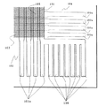
液晶表示装置は図6に示すように、基板上にセグメント側透明電極1を形成した第1のガラス基板2と、コモン側透明電極3を形成した第2のガラス基板4とを対向させてギャップを作り、その周辺部を接着して液晶を封入したもので、セグメント側透明電極1とコモン側透明電極3とが交差してできる画素からなる表示部5を構成し、各電極に所望の電圧を印加することにより、生じた電界で液晶の配向を変化させて表示を行うものである。
【0003】
そして、液晶表示装置の製造の場合、第1のガラス基板2と第2のガラス基板4とのギャップは所定の設計値に保つために、特定径のグラスファイバ−又は球状の物質等をスペ−サ−として両基板間に分散させてギャップの管理がなされていた。しかし、近年の液晶表示装置の性能向上と共に液晶層となるギャップの管理が重要な問題となってきた。即ち、TN(ツイストネマチイック)型液晶からSTN(ス−パ−ツイストネマチイック)型液晶となって部分的なギャップむらが存在する場合表示のむらとなり表示品質を悪くする大きな要因となってきた。従って、液晶表示装置の表示品質を向上させるには表示部全域にわたってギャップを均一に保持する必要性があった。
【0004】
そこで、特開昭63−26631号公報に開示の発明においては、電極等の凹凸が形成された基板を用いる場合、少なくともギャップ形成に関する領域にはほぼ均等に凹凸を形成すべく、特に接着部を横切る給電線が給電機能の設計上のみでは不要であり、本来設置する必要がない領域にも、例えば給電線と同一材料からなる開回路のダミ−配線による凹凸を形成してギャップの不均一の発生を防止している。従って、凸部の高さと、スペ−サ径で定められるギャップを表示全域にわたって均等に形成することができる。
【0005】
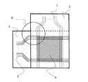
また、実開平2−128128号公報に開示の発明も、特開昭63−26631号公報と同様に、液晶表示装置の基板間のギャップの均一化のために、ダミ−電極を基板の非有効画素領域に配設することが開示されている。図7は実開平2−128128号公報に開示の液晶表示装置の構造を示したものである。図7(a)は図6のB部に相当する部分を示したもので、第1のガラス基板2と第2のガラス基板4上の隅角部に形成された電極の配置関係を示す要部平面図で、図7(b)は図7(a)のD−D線断面図である。
【0006】
図7から明らかなように、画素からなる表示部以外の非有効画素領域において、両基板上に対向する電極が存在しない場合には両基板上にダミ−電極が形成されている。即ち、セグメント側透明電極1もコモン側透明電極3も形成されていない基板部分には第1のガラス基板2にダミ−電極5a、5b、5cが形成され、第2のガラス基板4にはダミ−電極5a、5b、5cに対向する位置にダミ−電極6a、6b、6cが形成されている。又、一方基板にのみ電極がある場合にはその電極に対向する他方の基板の位置にダミ−電極が形成されている。即ち、第1のガラス基板2に形成されたセグメント側透明電極1に対向する第2のガラス基板4の位置にダミ−電極7a、7b、7cが形成されている。この結果、両基板間のギャップ間隔をダミ−電極を介して一定にするようにしている。
【0007】
【発明が解決しようとする課題】
しかしながら、上記の従来技術においては、基板間のギャップの不均一の発生を防止するためにダミ−電極を用いる場合、液晶表示装置完成後に、外部より静電気がチャ−ジされた後にその電荷がホ−ルドされ、非表示部分に常時点灯部が表示されてしまう様な新たな問題が発生した。又、液晶表示装置の画素電極部とダミ−電極部とで若干の色味が異なり、色むらが生ずるという問題があった。
【0008】
本発明は、上記の問題点に鑑みなされたもので、その目的は、液晶表示装置の基板間のギャップの均一化を図ると共に、静電気のチャ−ジによる非表示部分における常時点灯部の表示や色味など表示むらの改良をした液晶表示装置を提供することにある。
【0009】
【課題を解決するための手段】
上記目的を達成するために、本発明は、セグメント側透明電極を形成した第1基板とコモン側透明電極を形成した第2基板とを備え前記セグメント側透明電極と前記コモン側透明電極とが交差した画素からなる表示部をなし前記表示部の外周辺部にダミー電極を有する液晶表示装置において、
少なくとも前記外周辺部の4カ所の隅角部の少くとも一箇所のそれぞれの前記基板には対向する複数の前記ダミー電極が隅角部ダミー電極として形成されており前記隅角部ダミー電極は前記セグメント側透明電極と同様の電極で形成されあるいは前記コモン側透明電極と同様の電極で形成され且つ前記セグメント側透明電極または前記コモン側透明電極の電極幅と同じかまたは小さい電極幅で形成されており対向する前記第1基板または第2基板の一方の基板の前記隅角部ダミー電極は同じ基板上の前記画素を構成するための透明電極と接続され他方の基板の前記隅角部ダミー電極は前記画素を構成するための透明電極とは開回路のフローティング状態であることを特徴とする。
【0010】
さらに、前記接続電極で接続された前記ダミー電極は、前記第1の電極または前記第2の電極の最も外側であって、前記ダミ−電極と近い電極と前記接続電極で接続されていることを特徴とする。
【0011】
さらに、ダミ−電極は第1基板と第2基板が交差してできる領域の4カ所の隅角部の少なくとも一箇所に形成されていることを特徴とする。
【0012】
さらに、前記接続電極で接続された前記ダミー電極の電極幅は、前記接続電極で接続される前記第1の電極の電極幅または前記第2の電極の電極幅と略同じであることを特徴とする。
【0014】
【発明の実施の形態】
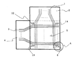
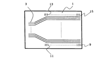
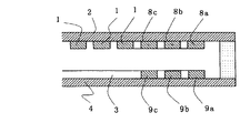
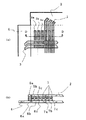
以下本発明の実施の形態を図面に示す実施例に基いて説明する。尚、図において、従来技術と同一部材は同一符号で示し、説明を省略する。図1は本発明の第1の実施例の液晶表示装置の電極の配置関係を示す平面図である。図2は図1の第2のガラス基板の電極の配置関係を示す平面図である。図3は図1のA部の拡大平面図である。図4は図3のC−C線断面図である。
【0015】
第1のガラス基板2の上に形成されたセグメント側透明電極1と第2のガラス基板4の上に形成されたコモン側透明電極3が交差してできる画素からなる表示部5以外の非有効画素領域にダミ−電極が形成されている。即ち、第1のガラス基板2にはダミ−電極8、10、12、14が4か所の隅角部に形成され、第2のガラス基板4にはダミ−電極8、10、12、14に対向した位置にダミ−電極9、11、13、15が形成されている。
図3のごとく、本発明の実施形態では、前記隅部に設けたダミー電極は、セグメント側透明電極1の電極幅あるいは電極ピッチとほぼ同じに設定した。
【0016】
また、ダミ−電極8、9についてみると、図4の断面図に示したように、ダミ−電極8a、8b、8cおよび9a、9b、9cは図4の断面図に示されるように、セグメント側透明電極1やコモン側透明電極3が存在していない基板上に設けられ、しかもダミ−電極8a−9a、8b−9b、8c−9c間のギャップ間隔はセグメント側透明電極1とコモン側透明電極3とのギャップ間隔と同じ距離にしてある。そして、第1のガラス基板2上のダミ−電極8、10、12、14はそれぞれセグメント側透明電極1の外側の電極に接続されて導通を取っているいる。ダミ−電極8についてみると、接続電極8dにより各ダミ−電極8a、8b、8cが外側のセグメント側透明電極1aに接続されている。第2のガラス基板4上のダミ−電極9、11、13、15は図2に示すように、コモン側透明電極3とは接続せずに非導通の開回路のフロ−ティングの状態にされている。
【0017】
この様な構成によって、第1の実施例においては、第1のガラス基板2と第2のガラス基板4のギャップはセグメント側透明電極1とコモン側透明電極3とでできるギャップの間隔が表示部の外周辺部においてはダミ−電極8−9、10−11、12−13、14−15間によって同じ間隔のギャップが設定されていることから、両基板間に特定径の球状等のスペ−サ−材として分散させることにより基板間のギャップを一定に且つ均一にすることができる。
【0018】
また、第1のガラス基板2上のダミ−電極8、10、12、14はそれぞれセグメント側透明電極1の電極と接続されていることから、液晶表示装置完成後外部よりダミ−電極部に静電気がチャ−ジされてもセグメント側透明電極を通して放電が可能であり、表示品質を劣化させることはない。
【0019】
更に、本実施例においては、第1のガラス基板2上のダミ−電極8、10、12、14はそれぞれセグメント側透明電極1の電極と接続し、第2のガラス基板4上のダミ−電極9、11、13、15はコモン側透明電極3とは接続せず開回路のフロ−ティングの状態にされている。
【0020】
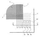
図5は本発明の他の実施例で、図1のA部に相当する部分を示した拡大平面図である。ダミ−電極を液晶表示パネルの表示部の外周辺部の4辺に沿って形成したものである。第1のガラス基板102上のダミ−電極は画素部を構成するセグメント側透明電極101を表示部105の外周辺部に延長してダミ−電極101aとし、図示はしていないが、ダミ−電極101aと対向するダミ−電極を第2のガラス基板104上に形成し、又、第2のガラス基板104上のダミ−電極は画素部を構成するコモン側透明電極103を表示部105の外周辺部に延長してダミ−電極103aとし、図示はしていないが、ダミ−電極103aと対向するダミ−電極を第1のガラス基板102上に形成したものである。尚、隅角部のダミ−電極108は第1の実施例と同様の構成で4カ所に設けられている。又、セグメント側透明電極又はコモン側透明電極を延長して形成するダミ−電極の幅はそれぞれセグメント側透明電極又はコモン側透明電極の表示部電極の幅より小さくしている。セグメント側透明電極の幅は120μm〜200μm程度で、コモン側透明電極の幅は300μm程度で、これを延長して形成するダミ−電極の幅はそれぞれの約90%程度が適当である。ダミ−電極の幅が余り小さくなると非点灯状態で表示部との識別がはっきりして好ましくない。尚、上記のセグメント側透明電極とコモン側透明電極の幅から画素の面積は300μm×120μm〜200μm程度である。
【0021】
この実施例では表示部105の外周片部の4辺すべてにダミ−電極が形成されているので基板のギャップ間隔を一定に且つ均一にする効果を一層高めることができる。又、セグメント側透明電極又はコモン側透明電極を延長して形成するダミ−電極の幅はそれぞれセグメント側透明電極又はコモン側透明電極の幅より小さくそれぞれの横のギャップを大きくしているのでダミ−電極部での電極間の短絡を防止することができる。
このように本発明は、一方の基板上にセグメント側透明電極を形成した第1基板と、他方の基板上にコモン側透明電極を形成した第2基板とを備え、前記第1基板と前記第2基板との間に液晶を封止してなる液晶表示装置であり、前記セグメント側電極と前記コモン側電極とが交差した画素からなる表示部以外の領域の前記第1基板及び前記第2基板に夫々対向する如くダミ−電極を形成し、前記第1基板上の前記ダミ−電極は前記セグメント側透明電極のいずれか1つの電極と接続すると共に、前記第2基板上の前記ダミ−電極は開回路としたこと、及び又は前記第2基板上の前記ダミ−電極は前記コモン側透明電極のいずれか1つの電極と接続すると共に、前記第1基板上の前記ダミ−電極は開回路とした。さらに、前記第1基板又は前記第2基板上の前記ダミ−電極は前記セグメント側透明電極又は前記コモン側透明電極の最も外側であって、前記ダミ−電極と近い電極と接続されている。さらに、前記ダミ−電極は前記第1基板と第2基板が交差してできる領域の4カ所の隅角部の少くとも一箇所に形成されている。さらに、前記ダミ−電極は前記表示部の外周辺部の4辺に沿って形成されている。さらに、前記表示部の外周辺部に、前記第1基板上の前記セグメント側透明電極を延長して形成される前記ダミ−電極の幅は前記セグメント側透明電極の表示部電極の幅より小さく、前記第2基板上の前記コモン側透明電極を延長して形成される前記ダミ−電極の幅は前記コモン側透明電極の表示部電極の幅より小さくしている。
【0022】
【発明の効果】
以上述べたことから明らかなように、本発明によれば、ダミ−電極を基板に設けることによって液晶表示装置の基板間のギャップの均一化を図ると共に、ダミ−電極の一方を画素電極に接続し、他方を開回路即ちフロ−ティングにしておくことにより色味など表示むらをなくすことができる効果を有する。
【図面の簡単な説明】
【図1】本発明の第1の実施例の液晶表示装置の電極の配置関係を示す平面図である。
【図2】図1の第2のガラス基板の電極の配置関係を示す平面図である。
【図3】図1のA部の拡大平面図である。
【図4】図3のC−C線断面図である。
【図5】本発明の他の実施例であり、図1のA部に相当する部分拡大平面図である。
【図6】従来の液晶表示装置の電極配置関係を示す平面図である。
【図7】図7(a)は図6のB部に相当する部分の電極配置関係を示す要部拡大平面図で、図7(b)は図7(a)のD−D線断面図である。
【符号の説明】
1、101 セグメント側透明電極
2、102 第1のガラス基板
3、103 コモン側透明電極
4、104 第2のガラス基板
5、105 表示部
8、10、12、14 第1のガラス基板上のダミ−電極
9、11、13、15 第2のガラス基板上のダミ−電極[0001]
BACKGROUND OF THE INVENTION
The present invention relates to a liquid crystal display device, and more particularly to improvement in display unevenness such as contrast and color tone due to gap unevenness in an STN (super twisted nematic) liquid crystal display device.
[0002]
[Prior art]
As shown in FIG. 6, the liquid crystal display device has a gap between a
[0003]
In the case of manufacturing a liquid crystal display device, in order to keep the gap between the
[0004]
Therefore, in the invention disclosed in Japanese Patent Application Laid-Open No. 63-26631, when using a substrate on which unevenness such as an electrode is formed, an adhesive portion is formed in order to form unevenness almost evenly in at least a region related to gap formation. Crossing the feeder line is not necessary only in the design of the feeder function, and unevenness due to open circuit dummy wiring made of the same material as the feeder line is formed in an area where it is not necessary to install the feeder line. Occurrence is prevented. Therefore, the gap defined by the height of the convex portion and the spacer diameter can be formed uniformly over the entire display area.
[0005]
In addition, the invention disclosed in Japanese Utility Model Laid-Open No. 2-128128 also provides a dummy electrode which is ineffective for the substrate in order to make the gap between the substrates of the liquid crystal display device uniform, as in Japanese Patent Laid-Open No. 63-26631. Disposing in the pixel region is disclosed. FIG. 7 shows the structure of a liquid crystal display device disclosed in Japanese Utility Model Laid-Open No. 2-128128. FIG. 7A shows a portion corresponding to part B of FIG. 6, and it is necessary to show the positional relationship between the electrodes formed at the corners on the
[0006]
As can be seen from FIG. 7, in the non-effective pixel region other than the display portion composed of pixels, when there are no opposing electrodes on both substrates, dummy electrodes are formed on both substrates. That is,
[0007]
[Problems to be solved by the invention]
However, in the above prior art, when a dummy electrode is used in order to prevent the occurrence of non-uniform gaps between the substrates, after the liquid crystal display device is completed, the charge is charged after the static electricity is charged from the outside. -A new problem has arisen in which a constantly lit portion is displayed in a non-display portion. In addition, the pixel electrode portion and the dummy electrode portion of the liquid crystal display device are slightly different in color and have a problem of uneven color.
[0008]
The present invention has been made in view of the above problems, and its purpose is to make the gap between the substrates of the liquid crystal display device uniform and to display a constantly lit portion in a non-display portion due to electrostatic charge. An object of the present invention is to provide a liquid crystal display device with improved display unevenness such as color.
[0009]
[Means for Solving the Problems]
In order to achieve the above object, the present invention comprises a first substrate on which a segment side transparent electrode is formed and a second substrate on which a common side transparent electrode is formed, and the segment side transparent electrode and the common side transparent electrode intersect. In a liquid crystal display device having a dummy electrode on the outer peripheral portion of the display unit, the display unit comprising the above-described pixels ,
A plurality of opposing dummy electrodes are formed as corner dummy electrodes on at least one of the substrates in at least one corner of the outer peripheral portion, and the corner dummy electrodes are It is formed of an electrode similar to the segment side transparent electrode or formed of an electrode similar to the common side transparent electrode and formed with an electrode width equal to or smaller than the electrode width of the segment side transparent electrode or the common side transparent electrode. The corner dummy electrode of one of the first substrate and the second substrate facing each other is connected to a transparent electrode for constituting the pixel on the same substrate, and the corner dummy electrode of the other substrate Is characterized in that the transparent electrode for constituting the pixel is in an open circuit floating state .
[0010]
Further, the dummy electrodes connected by the connecting electrode, the an outermost first electrode or the second electrode, the dummy - that is connected to the electrode and the closer electrode at the connecting electrode Features.
[0011]
Furthermore, dummy - electrode is characterized in that it is formed in small Do Kutomo one place corners of four positions of the area that can intersect first substrate and the second substrate.
[0012]
Furthermore, the electrode width of the dummy electrode connected by the connection electrode is substantially the same as the electrode width of the first electrode or the second electrode connected by the connection electrode, To do.
[0014]
DETAILED DESCRIPTION OF THE INVENTION
Embodiments of the present invention will be described below based on examples shown in the drawings. In the figure, the same members as those of the prior art are denoted by the same reference numerals, and description thereof is omitted. FIG. 1 is a plan view showing the positional relationship of electrodes of a liquid crystal display device according to a first embodiment of the present invention. FIG. 2 is a plan view showing the positional relationship of the electrodes of the second glass substrate of FIG. FIG. 3 is an enlarged plan view of a portion A in FIG. 4 is a cross-sectional view taken along the line CC of FIG.
[0015]
Ineffective other than the
As shown in FIG. 3, in the embodiment of the present invention, the dummy electrode provided at the corner is set to be substantially the same as the electrode width or electrode pitch of the segment side
[0016]
Further, regarding the
[0017]
With such a configuration, in the first embodiment, the gap between the
[0018]
Moreover, since the
[0019]
Furthermore, in this embodiment, the
[0020]
FIG. 5 is an enlarged plan view showing a portion corresponding to part A of FIG. 1 according to another embodiment of the present invention. The dummy electrodes are formed along the four sides of the outer peripheral part of the display part of the liquid crystal display panel. The dummy electrode on the
[0021]
In this embodiment, since dummy electrodes are formed on all four sides of the outer peripheral piece of the
As described above, the present invention includes the first substrate in which the segment-side transparent electrode is formed on one substrate, and the second substrate in which the common-side transparent electrode is formed on the other substrate, and the first substrate and the first substrate A liquid crystal display device in which liquid crystal is sealed between two substrates, and the first substrate and the second substrate in a region other than a display portion including pixels in which the segment side electrode and the common side electrode intersect. The dummy electrodes on the first substrate are connected to any one of the segment-side transparent electrodes, and the dummy electrodes on the second substrate are The dummy electrode on the second substrate is connected to any one of the common-side transparent electrodes, and the dummy electrode on the first substrate is an open circuit. . Further, the dummy electrode on the first substrate or the second substrate is connected to the outermost electrode of the segment side transparent electrode or the common side transparent electrode and close to the dummy electrode. Further, the dummy electrode is formed in at least one of the four corners of the region formed by the intersection of the first substrate and the second substrate. Furthermore, the dummy electrode is formed along four sides of the outer peripheral portion of the display unit. Furthermore, the width of the dummy electrode formed by extending the segment side transparent electrode on the first substrate on the outer periphery of the display unit is smaller than the width of the display unit electrode of the segment side transparent electrode, The dummy electrode formed by extending the common-side transparent electrode on the second substrate has a width smaller than that of the display portion electrode of the common-side transparent electrode.
[0022]
【The invention's effect】
As is apparent from the above description, according to the present invention, the dummy electrode is provided on the substrate to make the gap between the substrates of the liquid crystal display device uniform, and one of the dummy electrodes is connected to the pixel electrode. However, it is possible to eliminate display unevenness such as color by making the other open circuit, that is, floating.
[Brief description of the drawings]
FIG. 1 is a plan view showing an arrangement relationship of electrodes of a liquid crystal display device according to a first embodiment of the present invention.
2 is a plan view showing an arrangement relationship of electrodes of a second glass substrate of FIG. 1. FIG.
FIG. 3 is an enlarged plan view of a part A in FIG. 1;
4 is a cross-sectional view taken along the line CC in FIG. 3;
5 shows another embodiment of the present invention, and is a partially enlarged plan view corresponding to part A in FIG. 1. FIG.
FIG. 6 is a plan view showing an electrode arrangement relationship of a conventional liquid crystal display device.
7 (a) is an enlarged plan view of a main part showing the electrode arrangement relationship of a portion corresponding to the portion B in FIG. 6, and FIG. 7 (b) is a sectional view taken along the line DD in FIG. 7 (a). It is.
[Explanation of symbols]
DESCRIPTION OF SYMBOLS 1,101 Segment side transparent electrode 2,102 1st glass substrate 3,103 Common side transparent electrode 4,104 2nd glass substrate 5,105
Claims (1)
コモン側透明電極を形成した第2基板とを備え
前記セグメント側透明電極と前記コモン側透明電極とが交差した画素からなる表示部をなし
前記表示部の外周辺部にダミー電極を有する
液晶表示装置において、
少なくとも前記外周辺部の4カ所の隅角部の少くとも一箇所のそれぞれの前記基板には対向する複数の前記ダミー電極が隅角部ダミー電極として形成されており
前記隅角部ダミー電極は前記セグメント側透明電極と同様の電極で形成されあるいは前記コモン側透明電極と同様の電極で形成され
且つ前記セグメント側透明電極または前記コモン側透明電極の電極幅と同じかまたは小さい電極幅で形成されており
対向する前記第1基板または第2基板の一方の基板の前記隅角部ダミー電極は同じ基板上の前記画素を構成するための透明電極と接続され他方の基板の前記隅角部ダミー電極は前記画素を構成するための透明電極とは開回路のフローティング状態であることを特徴とする液晶表示装置。 A first substrate on which a segment-side transparent electrode is formed;
And a second substrate on which a common-side transparent electrode is formed
A display unit comprising pixels in which the segment-side transparent electrode and the common-side transparent electrode intersect
In the liquid crystal display device having a dummy electrode on the outer peripheral portion of the display unit,
A plurality of opposing dummy electrodes are formed as corner dummy electrodes on at least one of the substrates in at least one corner of the outer peripheral portion.
The corner dummy electrode is formed of an electrode similar to the segment side transparent electrode or an electrode similar to the common side transparent electrode.
And it is formed with an electrode width equal to or smaller than the electrode width of the segment side transparent electrode or the common side transparent electrode.
The corner dummy electrode of one of the first and second substrates facing each other is connected to a transparent electrode for constituting the pixel on the same substrate, and the corner dummy electrode of the other substrate is A liquid crystal display device characterized in that a transparent electrode for constituting a pixel is in an open circuit floating state .
Priority Applications (1)
| Application Number | Priority Date | Filing Date | Title |
|---|---|---|---|
| JP29148996A JP3819086B2 (en) | 1996-11-01 | 1996-11-01 | Liquid crystal display |
Applications Claiming Priority (1)
| Application Number | Priority Date | Filing Date | Title |
|---|---|---|---|
| JP29148996A JP3819086B2 (en) | 1996-11-01 | 1996-11-01 | Liquid crystal display |
Publications (2)
| Publication Number | Publication Date |
|---|---|
| JPH10133215A JPH10133215A (en) | 1998-05-22 |
| JP3819086B2 true JP3819086B2 (en) | 2006-09-06 |
Family
ID=17769538
Family Applications (1)
| Application Number | Title | Priority Date | Filing Date |
|---|---|---|---|
| JP29148996A Expired - Lifetime JP3819086B2 (en) | 1996-11-01 | 1996-11-01 | Liquid crystal display |
Country Status (1)
| Country | Link |
|---|---|
| JP (1) | JP3819086B2 (en) |
-
1996
- 1996-11-01 JP JP29148996A patent/JP3819086B2/en not_active Expired - Lifetime
Also Published As
| Publication number | Publication date |
|---|---|
| JPH10133215A (en) | 1998-05-22 |
Similar Documents
| Publication | Publication Date | Title |
|---|---|---|
| KR200162435Y1 (en) | Stn-lcd | |
| US5684555A (en) | Liquid crystal display panel | |
| KR19990042088A (en) | Liquid crystal display | |
| JP2002268079A (en) | Optoelectronic device and electronic apparatus | |
| JP3819086B2 (en) | Liquid crystal display | |
| KR101432891B1 (en) | Liquid Crystal Display Device | |
| KR20110070565A (en) | Liquid crystal display device and method for fabricating the same | |
| JP2921864B2 (en) | Liquid crystal display | |
| WO2022110151A9 (en) | Array substrate and touch-control display apparatus | |
| JP2000338514A (en) | Liquid crystal display device | |
| KR100272514B1 (en) | Ips mode lcd apparatus equipped with position detection function | |
| JPS6326631A (en) | Liquid crystal display device | |
| CN109828413B (en) | Display panel and electronic device | |
| JP2638713B2 (en) | Active matrix liquid crystal display | |
| JP3720134B2 (en) | Liquid crystal display device | |
| JPH11212117A (en) | Tft array substrate and liquid crystal display device provided with the substrate | |
| JP2875645B2 (en) | Liquid crystal display device | |
| JPH0324523A (en) | Electrooptical display cell | |
| KR20040103275A (en) | In-Plane Switching Mode Liquid Crystal Display device and method for fabricating the same | |
| JPH10228026A (en) | Liquid crystal display device | |
| JPH08286213A (en) | Liquid crystal display device | |
| KR100446212B1 (en) | Liquid Crystal Display Device | |
| WO2022217885A1 (en) | Display panel and manufacturing method therefor, and display device | |
| JP2987760B2 (en) | Liquid crystal display | |
| JP3150621B2 (en) | LCD panel |
Legal Events
| Date | Code | Title | Description |
|---|---|---|---|
| A977 | Report on retrieval |
Free format text: JAPANESE INTERMEDIATE CODE: A971007 Effective date: 20050324 |
|
| A131 | Notification of reasons for refusal |
Free format text: JAPANESE INTERMEDIATE CODE: A131 Effective date: 20050510 |
|
| A521 | Written amendment |
Free format text: JAPANESE INTERMEDIATE CODE: A523 Effective date: 20050629 |
|
| A131 | Notification of reasons for refusal |
Free format text: JAPANESE INTERMEDIATE CODE: A131 Effective date: 20060207 |
|
| A521 | Written amendment |
Free format text: JAPANESE INTERMEDIATE CODE: A523 Effective date: 20060410 |
|
| TRDD | Decision of grant or rejection written | ||
| A01 | Written decision to grant a patent or to grant a registration (utility model) |
Free format text: JAPANESE INTERMEDIATE CODE: A01 Effective date: 20060613 |
|
| A61 | First payment of annual fees (during grant procedure) |
Free format text: JAPANESE INTERMEDIATE CODE: A61 Effective date: 20060614 |
|
| S533 | Written request for registration of change of name |
Free format text: JAPANESE INTERMEDIATE CODE: R313533 |
|
| R350 | Written notification of registration of transfer |
Free format text: JAPANESE INTERMEDIATE CODE: R350 |
|
| FPAY | Renewal fee payment (event date is renewal date of database) |
Free format text: PAYMENT UNTIL: 20100623 Year of fee payment: 4 |