JP3776232B2 - Natural frequency measuring device and tension measuring device - Google Patents
Natural frequency measuring device and tension measuring device Download PDFInfo
- Publication number
- JP3776232B2 JP3776232B2 JP05889498A JP5889498A JP3776232B2 JP 3776232 B2 JP3776232 B2 JP 3776232B2 JP 05889498 A JP05889498 A JP 05889498A JP 5889498 A JP5889498 A JP 5889498A JP 3776232 B2 JP3776232 B2 JP 3776232B2
- Authority
- JP
- Japan
- Prior art keywords
- natural frequency
- gain
- measuring device
- waveform
- amplification
- Prior art date
- Legal status (The legal status is an assumption and is not a legal conclusion. Google has not performed a legal analysis and makes no representation as to the accuracy of the status listed.)
- Expired - Lifetime
Links
Images


Description
【0001】
【発明の属する技術分野】
本発明は固有振動数測定装置および張力測定装置に関し、特に、2点間に架けられた帯状および線状物体等の固有振動数を測定する測定装置および固有振動数に基づいて張力測定する張力測定装置に関する。
【0002】
【従来の技術】
動力を伝達したり物品を搬送したりするためベルト装置が使用されることが多い。このベルト装置においては、使用されているベルトの張力は予定の値を維持するよう管理されていて、ベルト張力が予定値から外れると、動力の伝達効率が低下したり搬送状態の安定性が損なわれたりする。また、ベルトの特性にあった張力が与えられていないと、ベルト自体の寿命も低下する。
【0003】
このようなベルト張力の管理の重要性に鑑み、本出願人は、ベルト張力を簡易に測定できる張力測定装置を提案している(特公平6−63825号公報)。この張力測定装置は、マイクロフォン(以下、単に「マイク」という)で検出された被測定物(ベルト)の振動波形の周期を測定する手段と、測定された周期の変動が予定範囲内にある連続した複数の波形からなる波形群を特定する手段と、この波形群を代表する波形の周期または周波数に基づいて張力を演算する手段とから構成されている。
【0004】
2点間に張られたベルトに衝撃を加えて振動させると、このベルトは当初、高調波成分や衝撃成分を含んだ不規則な波形で振動するが、やがて時間の経過とともにそのベルトに固有の規則的な波形、すなわち、基本波形のみの固有振動数で振動するようになる。
【0005】
上記張力測定装置は、このような現象の実験的確認に鑑みてなされたもので、前記固有振動による規則的な波形(すなわち周期の変動が予定範囲内にある波形)が連続した波形群を固有振動による規則的な波形として検出する。そして、この波形の周期に基づいて固有振動数が算出され、さらにこの固有振動数に基づいてベルト張力が算出される。
【0006】
【発明が解決しようとする課題】
上記の張力測定装置では、解決すべき次の課題がある。上記張力測定装置において、マイクで音波としてとらえられたベルトの振動は、その振動周期を測定する処理のため、予定のスレッショルドレベルに従って波形整形される。ベルトの振動はマイクの増幅器によって増幅された後、前記波形整形器に入力される。
【0007】
ここで、前記増幅器の感度が低いと、入力される振動レベルがスレッショルドレベルに達せず、波形整形器によって正しい出力が得られない。一方、前記増幅器の感度が高すぎた場合には、暗騒音を拾ってしまう。このため、増幅器のゲインを適正値に設定する必要があり、例えば、入力信号がスレッショルドレベルを超過したかどうかを示す表示灯を設け、この表示灯の点灯状態を監視しながらゲイン調整をすることが考えられる。
【0008】
しかし、このように表示灯を監視しながら手動でゲイン調整を行うのは、測定者にとって負担が大きいだけでなく、測定者によって判断のばらつきが生じるおそれがあり、張力を常に正確な値に管理することができないという問題点がある。
【0009】
本発明は、上記課題を解決するためになされたものであり、暗騒音の影響を自動的に排除して被測定物の振動を正しく検知できるようにした固有振動数測定装置および張力測定装置を提供することを目的とする。
【0010】
【課題を解決するための手段】
上記の問題点を解決するための本発明は、マイクで検出された被測定物の振動波形に基づいて該被測定物の固有振動数を測定する固有振動数測定装置において、前記マイクで検出された振動波形を増幅する増幅手段と、前記増幅手段で増幅された振動波形を予定のスレッショルドに従って波形整形する波形整形手段と、前記波形整形手段で波形整形された振動波形に基づいて前記被測定物の固有振動数を検出する演算手段と、前記波形整形手段から出力される振動波形から暗騒音のレベルを検出する暗騒音レベル検出手段と、前記暗騒音レベルが基準レベルより高い場合は低い方に、該暗騒音レベルが基準レベルより低い場合は高い方に前記増幅手段の増幅ゲインを自動調整するゲイン調整手段とを具備した点に特徴がある。
【0011】
この特徴によれば、暗騒音レベルが高い場合は入力される振動波形の増幅ゲインを小さくでき、暗騒音レベルが低い場合は入力される振動波形の増幅ゲインを大きくできるので、マイクから入力される暗騒音の波形信号を、被測定対象の振動波形の検出の障害とならない限界まで低下できる。
【0012】
【発明の実施の形態】
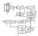
以下に、図面を参照して、本発明を詳細に説明する。図1は本発明の一実施例を示す張力測定装置のハード構成を示すブロック図である。図1において、軸間距離Lで配置されたプーリ1a,1bに架けられているベルト2に対向してマイク3が配置されている。マイク3で検出された波動は、フィルタ4に入力される。フィルタ4では、入力された波形信号から高周波のノイズ成分を除去する。ノイズが除去された波形信号は増幅器12で増幅された後、コンパレータ5に供給される。コンパレータ5は、スレッショルドに従って入力波形を2値化信号に変換する波形整形手段であって、矩形波信号を出力する。増幅器12にはゲイン調整器13が設けられており、コンパレータ5の出力波形に基づいて自動的に増幅器12のゲインを調整する。
【0013】
前記コンパレータ5の出力信号は微分回路6に入力され、この微分回路6は、波形の立上がりおよび立下がりのエッジ検出信号を出力する。このエッジ検出信号のうち、例えば立上がりのエッジ検出信号が、遅延回路7、ラッチ8、およびフリップフロップ(F/F)9に入力される。クロックカウンタ10は、図示しないパルス発生装置から供給されるクロックパルス(CK)を計数する。前記エッジ検出信号に応答して、ラッチ8はクロックカウンタ10の値を取込む。また、遅延回路7は前記エッジ検出信号を所定時間遅らせてクロックカウンタ10に供給する。遅延された信号はクロックカウンタ10のリセット端子に接続され、遅延された信号によってクロックカウンタ10の値がリセットされる。
【0014】
フリップフロップ9は、前記エッジ検出信号によってセットされる。フリップフロップ9の出力状態は、マイコン11で識別される。マイコン11はフリップフロップ9のセットを検出し、これによってクロックカウンタ10の値がラッチ8に保持されたことを認識する。マイコン11は、この認識結果に基づいてラッチ8からカウンタ値を取込み、該マイコン11内のメモリに格納する。マイコン11はカウンタ値をラッチ8から取込んだ後はクリア信号を出力してフリップフロップ9をリセットする。前記マイコン11内のメモリには、マイク3で検出された振動波形に基づいて得られたコンパレータ5の出力波形(矩形波)の1サイクル毎の周期が、クロックカウンタ10のカウンタ値として記憶される。
【0015】
以上の構成において、図示しない打撃手段でベルト2に衝撃を加えると、この衝撃によるベルト2の振動はマイク3で検出され、この振動の各サイクルの周期が前記マイコン11内に記憶される。ベルト2の振動は、最初は衝撃や高調波成分を含んだ不規則な波形であるが、しだいに規則的な波形が連続するようになり、この波形が、プーリ1a,1bに架けられたベルト2の固有振動数と認められる。マイコン11は、取込んだカウンタ値に基づいて規則的な波形すなわち固有振動数を検出する機能、および検出された規則的な波形の周波数に基づいて所定の張力算出式によりベルト2の張力を算出する機能を有する。これらの機能は、前記特公平6−63825号公報に詳細に開示されており、かつ本発明の要部ではないので説明は省略する。
【0016】
次に、前記ゲイン調整器13の具体例を説明する。まず、ゲイン調整器13の動作概要を説明する。ゲイン調整器13では、コンパレータ5の出力信号を一定時間監視する。この監視動作は、例えば、前記ベルト2の張力測定前に実行される。この監視動作により、コンパレータ5の出力信号が予定の回数以上現れるような場合、つまり暗騒音検出レベルが高い場合には増幅器12のゲインを低下させる。一方、検出されたコンパレータ5の出力信号が予定の回数以下であれば、暗騒音検出レベルが低く、所望の振動波形をも検出できないおそれがあるためゲインを増大させる。例えば、コンパレータ5のスレッショルドを超えるような信号が全く検出されないようであればゲインを上げ、一方、このような信号が3回以上検出されるようであればゲインを下げる。
【0017】
図8は、ゲイン調整器13の動作を説明するための図であり、暗騒音の波形の一例を示す図である。同図において、暗騒音を一定時間Tの間抽出する。この時間Tはベルト2等の被測定物の固有振動数の周期の最大値に設定するのがよい。すなわち、被対象物の固有振動の最大周期内に数個検出されるだけの暗騒音は、その周期よりも小さい周期(つまり高周波数)である被測定物の固有振動数を測定する時の障害にはならないからである。例えば、被測定物の固有振動数の周波数が10〜300Hzである場合を想定すると、最大周期は周波数10Hzに対応する時間、つまり0.1秒となる。この時間T内にスレッショルドThを超過する暗騒音の波形のピークPが予定回数(例えば2回)検出される程度にゲインを設定するのがよい。
【0018】
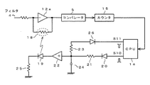
図2は、ゲイン調整器13の具体的な構成を示す回路図である。同図において、増幅器としてのオペアンプ12のゲインを決定するため、該オペアンプ12のマイナス入力と接地間に抵抗R0が設けられ、かつオペアンプ12の出力およびマイナス入力間には抵抗R1,R2,R3,R4が設けられている。これらの抵抗R0〜R4によって、(R1+R2+R3+R4)/R0で算出される値に比例したゲインが与えられる。各抵抗R1〜R4の両端にはスイッチSW1,SW2,SW3,SW4がそれぞれ設けられており、これらのスイッチの切替えによってゲインが調整される。スイッチSW1〜SW4はCPU14から各スイッチSW1〜SW4に入力される信号s1〜s4が「1」のときに「閉」側に切替えられる。すべてのスイッチSW1〜SW4が閉じた時、つまり抵抗R1,R2,R3,R4の合成抵抗値Rが「0」のときにゲインは最小値に設定される。
【0019】
カウンタ15はコンパレータ5の出力信号のハイレベルつまり「1」の数を計数し、予め設定された時間T毎に計数値Cを出力する。CPU14はカウンタ15から入力された計数値に従って信号s1〜s4の組み合わせを変化させてオペアンプ12のゲインを調整する。例えば、初期状態ではゲインが中程度となるように信号s1〜s4の値を決定しておき、前記計数値に応じてゲインを増減する。
【0020】
図3は、前記計数値に応じてゲインを調整するためのCPU14の要部機能を示すブロック図である。同図において、比較部141はカウンタ15からの計数値Cを基準値Cref と比較する。この比較結果により、計数値Cの方が大きい場合はゲインを下げる信号decを出力し、計数値Cの方が小さい場合はゲインを上げる信号incを出力する。組合せ設定部142はこれらの信号decまたはincに応答して、前記信号s1〜s4の値の組み合わせを、ゲインを上下させるための予定の組合せに設定する。信号s1〜s4の組み合わせにより「0000」〜「1110」まで15通りのゲインを設定できる。信号s1〜s4が「0000」のときゲインは最大となり、信号s1〜s4が「1110」のときゲインは最小となる。
【0021】
なお、前記基準値Cref に不感帯つまり最適範囲を設けておき、この不感帯の範囲内であればゲインを変化させないようにすることもできる。具体的には基準値Cref を2段階設けて、その段階の間を最適範囲とするとよい。
【0022】
また、前記基準値Cref 複数段階設け、各段階の基準値Cref と計数値Cとを比較し、その大小の判断結果により増減するゲインの幅を変化させるようにしてもよい。例えば、計数値Cが、高低2段階の基準値Cref の低い方よりもさらに小さい場合のゲイン増大量をGinc1とし、計数値Cが、低い方の基準値Cref よりは大きいが、高い方の基準値Cref よりは小さい場合のゲイン増大量をGinc2としたとき、「ゲイン増大量Ginc1>ゲイン増大量Ginc2」のように設定する。こうすることにより、少ないゲイン調整回数で早く所望のゲインを設定することができる。さら基準値Cref の段階を増やすことによって計数値Cが最適範囲より大きい場合にゲインを下げることができる構成を負荷できるのはもちろんである。
【0023】
上記第1の実施形態は、次のように変形できる。上述のように、比較部141の比較結果により信号s1〜s4の組み合わせを1段階ずつ変化させた場合、暗騒音のレベルによっては多数回のゲイン調整が必要なことがあり、複数段階の基準値Cref を設けても、必ずしも1回では最適なゲインを選択できないことがある。したがって、適当なゲイン選択のためには、コンパレータ5の信号の計数値を複数回読み込んで処理する必要が生じる。最適なゲインを予測することができれば、少ない回数の処理で適当なゲインを選択することができる。そこで、第1の実施形態を次のように変形して、最適なゲイン調整量を予測できるようにした。
【0024】
図4は上記実施形態の変形例を示す図である。この変形例では、コンパレータ5およびカウンタ15に加えて、第2のコンパレータ16と第2のカウンタ17を設け、第2のコンパレータ16のスレッショルドTh2をコンパレータ5のスレッショルドThよりも小さい値に設定した。こうしておいて、CPU14では2つのカウンタ15,17からの値をそれぞれ基準値Cref と比較するようにする。
【0025】
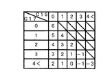
この比較の結果得られたカウンタ15および第2のカウンタ17双方からの計数値に基づいて最適なゲイン調整量を決定する。図13は、最適なゲイン調整量を決定するために用いるテーブルの一例である。同図において、カウンタ15の計数値C15と第2のカウンタ17の計数値C17の交差位置の値が最適なゲインである。例えば、計数値C15が「0」で計数値C17が「2」ならばゲインを4ステップ上げ、計数値C15が「2」で計数値C17が「3」ならばゲインを1ステップ上げる。また、計数値C15が「3」で計数値C17が「4以上」ならばゲインを1ステップ下げる。
【0026】
このように、暗騒音のレベルによりゲインの調整量を変化させるようにすれば、少ない回数で最適なゲインを設定することができる。なお、計数値C15と計数値C17とに基づいてテーブルを参照してゲインを決定するのではなく、計数値C15と計数値C17とに基づいて予定の算出式を使用し、演算によりゲインを決定してもよい。
【0027】
上述の例では、抵抗R0〜R4を直列接続したが、これらは並列接続でもよく、要は、増幅手段の帰還回路中に設けられた複数の抵抗の合成抵抗がスイッチ手段によって切り替えられるようになっていればよい。
【0028】
次に、本発明の第2実施形態を説明する。上述の実施形態では、複数の抵抗R1〜R4の組み合わせによってゲインを調整したが、この第2実施形態では、前記抵抗R1〜R4に代えて光量に応じて抵抗値が変化する光電変換素子を使用し、この光電変換素子の抵抗値によってオペアンプのゲインを調整するようにした。
【0029】
図5は、第2実施形態に係るゲイン調整器の構成を示す図である。同図において、オペアンプ12aの出力および入力間に光電変換素子18を設けた。光電変換素子18としては例えば硫化カドミウム(CdS)を使用できる。前記光電変換素子18との組み合わせでフォトカプラを構成するLED19が設けられ、CPU14は計数値Cに応じて前記LED19の光量を増大させるための信号s10または前記LED19の光量を低減させるための信号s11を出力する。
【0030】
CPU14の、信号s10の出力端子にはダイオード20のアノードが接続され、該ダイオード20のカソードは抵抗21の一端に接続されている。抵抗21の他端はオペアンプ22のプラス入力に接続され、さらに該プラス入力には抵抗23と、接地されたコンデンサ24とが接続されている。オペアンプ22の出力は前記LED19のアノードに接続され、該LED19のカソードは抵抗25を介して接地されている。前記オペアンプ22に接続された抵抗23の他端はダイオード26のアノードに接続され、該ダイオード26のカソードは前記CPU14の、信号s11の出力端子と接続されている。
【0031】
CPU14からプラス信号s10が出力されると、前記コンデンサ24には信号s10の入力に応じて電荷が蓄積される。その結果、LED19の電流が増大して、光電変換素子18の抵抗値が低下し、オペアンプ12のゲインが低下する。コンデンサ24に蓄積される電荷は信号s10の出力回数に応じて段階的に上昇し、それに伴ってオペアンプ12のゲインも段階的に増大する。一方、CPU14から出力されるマイナス信号s11によって、前記コンデンサ24に蓄積された電荷は放電する。コンデンサ24への電荷の蓄積量およびコンデンサ24からの電荷の放電量はコンデンサ24と抵抗21または抵抗23の時定数によって決定できる。
【0032】
上記構成により、オペアンプ12aのゲインを適正値に調整するためのCPU14の要部機能を図6に示す。本実施形態においても、第1実施形態と同様、コンパレータ5から出力される信号の「1」の数をカウンタ15によって計数するように構成し、図6に示すように、その計数値CをCPU14の比較部29に入力する。比較部29は前記計数値Cを基準値Cref と比較し、比較の結果、計数値Cの方が小さい場合は信号s10を出力し、計数値Cの方が大きい場合は信号s11を出力する。
【0033】
続いて、本発明の第3実施形態を説明する。ベルト2等の張力測定のためにその振動を測定する場合、振動波形の高調波成分は不要であり、かつ誤検知の要因となる。そこで、前記増幅器(オペアンプ)12では、不要な高調波成分をカットするようにすることが望ましい。この第3実施形態ではオペアンプ12の周波数−ゲイン特性(以下、単に「周波数特性」という)を変化させて、ベルト張力測定に不要な高調波成分をカットするようにした。
【0034】
図12は、オペアンプ12の周波数特性の一例を示す図である。同図(a)に示す周波数特性において、被測定物つまりベルト等の測定対象周波数fm よりも高い周波数の騒音も高い増幅ゲインで増幅されることになる。そこで、図12(b)のように、カットオフ周波数領域(最大ゲインからゲインが下がっている領域)に測定対象周波数fm が包含されるように周波数特性を変化させる。こうすることによって、測定対象周波数fm 以上の振動に対してはゲインを小さくすることができ、不必要な高調波成分をカットすることができる。
【0035】
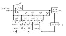
図7は、周波数特性を変化させるための要部回路図であり、図5と同符号は同一または同等部分を示す。ここでは、抵抗でゲインを調整するのに代えて、コンデンサの変化により測定周波数近傍でのゲイン調整をするようにしている。すなわち、オペアンプ12aの入力および出力間には抵抗Rが接続されているほか、コンデンサC1,C2,C3,C4,C5が直列に接続されている。また、コンデンサC1〜C5はスイッチSW10,SW11,SW12,SW13によって選択的に短絡させることができるように構成されている。
【0036】
スイッチSW10〜SW13を閉じてコンデンサの容量を大きくしていくに従い、カットオフ周波数が低周波数側に移動するように周波数特性が変化する。オペアンプ12aの最大ゲインは抵抗Rによって決定されている。
【0037】
スイッチSW10〜SW13は、CPU14からの信号s1〜s4によって開閉するが、ここでは、図2の場合とは異なり、信号s1〜s4が「1」のときにはスイッチSW10〜SW13が閉じるように構成する。信号s1〜s4が「1」のときにスイッチSW10〜SW13が閉じると、カットオフ周波数が高周波数側に移動して測定対象周波数でのゲインは高くなるように制御される。コンデンサC1〜C5の容量比を、2進数の比「1:2:4:8:16」に設定すれば、少ないコンデンサの数でより多段階にゲインを調整することができる。なお、この第3実施形態によれば、コンパレータ5に入力される波形から高調波成分がカットされるので、フィルタ4(図1)は省略することができる。
【0038】
以上のように構成された張力測定器によって暗騒音を排除してベルト2の張力を測定する際の操作手順の一例を説明する。図9は張力測定器の操作パネルを示す図であり、図10は操作手順の一例を示すフローチャートである。ステップS1では、張力測定器の電源スイッチ100をオンにする。この操作によって、マイク3から入力された波形信号のうち、コンパレータ5のスレッショルドを超過する暗騒音の波形信号のピーク数が前記CPU14に読み込まれ、前記ゲイン調整器13によって暗騒音を排除するためのゲイン調整が行われる。ステップS2では、前記電源スイッチ100とは別に、測定用に設けたスイッチ(測定スイッチ)110をオンにする。この測定スイッチのオン操作によってゲインは固定され、その後に入力される信号波形に基づいて,前記マイコン11でベルトの振動数が検出され、それに基づいてベルト張力が算出される。算出されたベルト張力の値は表示画面120に表示される。
【0039】
なお、上述の実施形態では、CPU14は一定時間内にスレッショルドを超過した信号が予定個数となるようにゲインを調整するようにしたが、このほか、予定時間内に検出された暗騒音の、それぞれのピーク間隔つまりコンパレータ5の出力波形の周期に基づいてゲインを設定することができる。すなわち、被測定物の固有振動数として予定される振動の最大周期を基準値として、該基準値よりも前記ピーク間隔が小さい場合は暗騒音が多く検出されていると判断してゲインを低減させる。また、該基準値よりも前記ピーク間隔が大きい場合は検出される暗騒音が少ないことを意味し、測定時のベルトの振動波形をも検出できないおそれがあるので、この場合はゲインを増大させる。
【0040】
図11は、信号間隔を検出するためのCPU14の要部機能を示す図である。同図において、コンパレータ5の出力信号を一定時間Tの間カウンタ27に入力する。カウンタ27はクロックCKを計数しており、コンパレータ5からの入力に応答してそのときの計数値PCを出力するとともに、その出力に応答して予定の遅延時間後に該カウンタ27はリセットされる。計数値PCは間隔判別部28に入力される。一定時間T内に間隔判別部28に入力された計数値PCは、基準の間隔PCref と比較され、該基準の間隔PCref よりも小さい計数値PCが存在している場合は、信号decを出力する。CPU14は、この信号decに基づいて、オペアンプ12,12aのゲインを下げげるように、図2のスイッチSW1〜SW4や、図7のスイッチSW10〜SW13等を切り替えるように構成する。
【0041】
また、基準の間隔PCref よりも小さい計数値PCが存在しなくなった場合は、検出信号incを出力する。CPU14は、この信号incに基づいて、オペアンプ12,12aのゲインを上げるように、図2のスイッチSW1〜SW4や、図7のスイッチSW10〜SW13等を切り替えるように構成する。なお、基準の間隔PCref は不感帯を有する最適範囲として設定し、計数値PCがこの不感帯から外れたときにゲインを変化されるようにすることもできる。
【0042】
なお、ゲインの設定段数すなわちスイッチSW1〜SW4やスイッチSW10〜SW13を切換える信号s1〜s4は上記実施例に示した数に限らず、増減してもよいのはもちろんである。
【0043】
【発明の効果】
以上の説明から明らかなように、本発明によれば、暗騒音の影響を受けないで、被対象物体の振動を検出することができるので、正確な固有振動数およびそれに基づく張力測定結果を得ることができる。
【図面の簡単な説明】
【図1】 本発明の一実施形態に係る測定装置のハード構成を示すブロック図である。
【図2】 第1実施形態のゲイン調整器のハード構成ブロック図である。
【図3】 ゲイン調整器の要部機能を示す図である。
【図4】 第1実施形態の変形例に係るゲイン調整器のハード構成ブロック図である。
【図5】 第2実施形態の変形例に係るゲイン調整器のハード構成ブロック図である。
【図6】 ゲイン調整器の要部機能を示す図である。
【図7】 第3実施形態の変形例に係るゲイン調整器のハード構成ブロック図である。
【図8】 暗騒音の波形の一例を示す図である。
【図9】 張力測定器の操作パネルを示す図である。
【図10】 張力測定器の操作手順の一例を示すフローチャートである。
【図11】 暗騒音の信号間隔を検出するための要部機能を示す図である。
【図12】 周波数特性の一例を示す図である。
【図13】 最適ゲイン設定テーブルの一例を示す図である。
【符号の説明】
1a,1b…プーリ、 2…ベルト、 3…マイク、 4…フィルタ、 5…コンパレータ。 12…増幅器、 13…ゲイン調整器、 14…CPU[0001]
BACKGROUND OF THE INVENTION
The present invention relates to a natural frequency measuring device and a tension measuring device, and in particular, a measuring device that measures a natural frequency of a band-like or linear object, etc., spanned between two points, and a tension measurement that measures tension based on the natural frequency. Relates to the device.
[0002]
[Prior art]
A belt device is often used to transmit power or convey articles. In this belt device, the tension of the belt being used is managed so as to maintain a predetermined value. If the belt tension deviates from the predetermined value, the power transmission efficiency is lowered or the stability of the conveyance state is impaired. Or Further, if the tension suitable for the characteristics of the belt is not applied, the life of the belt itself is also reduced.
[0003]
In view of the importance of such belt tension management, the present applicant has proposed a tension measuring device that can easily measure belt tension (Japanese Patent Publication No. 6-63825). This tension measuring device includes means for measuring a period of a vibration waveform of an object to be measured (belt) detected by a microphone (hereinafter simply referred to as a “microphone”), and a continuous variation in the measured period within a predetermined range. And a means for calculating a tension based on a period or a frequency of a waveform representative of the waveform group.
[0004]
When an impact is applied to a belt stretched between two points and it is vibrated, this belt initially vibrates with an irregular waveform containing harmonic components and impact components. It vibrates at a natural waveform, that is, a natural frequency of only a basic waveform.
[0005]
The above tension measuring device was made in view of the experimental confirmation of such a phenomenon, and a group of waveforms in which a regular waveform (that is, a waveform whose period variation is within a predetermined range) due to the natural vibration is continued. It is detected as a regular waveform due to vibration. The natural frequency is calculated based on the period of the waveform, and the belt tension is calculated based on the natural frequency.
[0006]
[Problems to be solved by the invention]
The above tension measuring device has the following problems to be solved. In the tension measuring device, the vibration of the belt captured as a sound wave by the microphone is shaped according to a predetermined threshold level for the process of measuring the vibration period. The vibration of the belt is amplified by a microphone amplifier and then input to the waveform shaper.
[0007]
Here, if the sensitivity of the amplifier is low, the input vibration level does not reach the threshold level, and a correct output cannot be obtained by the waveform shaper. On the other hand, if the sensitivity of the amplifier is too high, background noise is picked up. For this reason, it is necessary to set the gain of the amplifier to an appropriate value. For example, an indicator lamp that indicates whether the input signal has exceeded the threshold level is provided, and the gain is adjusted while monitoring the lighting state of the indicator lamp. Can be considered.
[0008]
However, manual gain adjustment while monitoring the indicator light in this way is not only burdensome for the measurer, but also may cause judgment variations by the measurer, and the tension is always managed to an accurate value. There is a problem that cannot be done.
[0009]
The present invention has been made to solve the above-described problems, and includes a natural frequency measurement device and a tension measurement device that can automatically detect the vibration of an object to be measured by automatically eliminating the influence of background noise. The purpose is to provide.
[0010]
[Means for Solving the Problems]
The present invention for solving the above-mentioned problems is a natural frequency measurement device that measures the natural frequency of a device under test based on the vibration waveform of the device under test detected with a microphone. Amplifying means for amplifying the vibration waveform, waveform shaping means for shaping the vibration waveform amplified by the amplification means according to a predetermined threshold, and the object to be measured based on the vibration waveform shaped by the waveform shaping means Calculating means for detecting the natural frequency, background noise level detecting means for detecting the level of background noise from the vibration waveform output from the waveform shaping means, and if the background noise level is higher than a reference level, the lower one Further, when the background noise level is lower than the reference level, a gain adjustment means for automatically adjusting the amplification gain of the amplification means is provided on the higher side.
[0011]
According to this feature, when the background noise level is high, the amplification gain of the input vibration waveform can be reduced, and when the background noise level is low, the amplification gain of the input vibration waveform can be increased. The waveform signal of background noise can be reduced to a limit that does not hinder the detection of the vibration waveform of the measurement target.
[0012]
DETAILED DESCRIPTION OF THE INVENTION
Hereinafter, the present invention will be described in detail with reference to the drawings. FIG. 1 is a block diagram showing a hardware configuration of a tension measuring apparatus according to an embodiment of the present invention. In FIG. 1, a
[0013]
The output signal of the
[0014]
The flip-
[0015]
In the above configuration, when an impact is applied to the
[0016]
Next, a specific example of the
[0017]
FIG. 8 is a diagram for explaining the operation of the
[0018]
FIG. 2 is a circuit diagram showing a specific configuration of the
[0019]
The counter 15 counts the high level of the output signal of the
[0020]
FIG. 3 is a block diagram showing the main functions of the
[0021]
It is also possible to provide a dead zone, that is, an optimum range for the reference value Cref, so that the gain is not changed within the dead zone range. Specifically, the reference value Cref may be provided in two stages, and the optimum range may be set between these stages.
[0022]
Further, the reference value Cref may be provided in a plurality of stages, the reference value Cref of each stage may be compared with the count value C, and the gain range to be increased or decreased may be changed according to the determination result. For example, Ginc1 is the gain increase amount when the count value C is smaller than the lower one of the reference values Cref of the two levels of high and low, and the count value C is larger than the lower reference value Cref but higher. When the gain increase amount is smaller than the value Cref and the gain increase amount is Ginc2, the gain increase amount Ginc1> the gain increase amount Ginc2 is set. In this way, a desired gain can be set quickly with a small number of gain adjustments. Furthermore, by increasing the step of the reference value Cref, it is possible to load a configuration that can reduce the gain when the count value C is larger than the optimum range.
[0023]
The first embodiment can be modified as follows. As described above, when the combination of the signals s1 to s4 is changed one step at a time according to the comparison result of the comparison unit 141, gain adjustment may be required many times depending on the background noise level. Even if Cref is provided, an optimum gain may not always be selected once. Therefore, in order to select an appropriate gain, it is necessary to read and process the count value of the signal of the comparator 5 a plurality of times. If an optimum gain can be predicted, an appropriate gain can be selected with a small number of processes. Therefore, the first embodiment is modified as follows so that the optimum gain adjustment amount can be predicted.
[0024]
FIG. 4 is a diagram showing a modification of the above embodiment. In this modification, in addition to the
[0025]
The optimum gain adjustment amount is determined based on the count values from both the
[0026]
As described above, if the gain adjustment amount is changed according to the background noise level, the optimum gain can be set with a small number of times. Instead of determining the gain by referring to the table based on the count value C15 and the count value C17, the gain is determined by calculation using a predetermined calculation formula based on the count value C15 and the count value C17. May be.
[0027]
In the above example, the resistors R0 to R4 are connected in series, but they may be connected in parallel. In short, the combined resistance of a plurality of resistors provided in the feedback circuit of the amplifying means is switched by the switch means. It only has to be.
[0028]
Next, a second embodiment of the present invention will be described. In the above-described embodiment, the gain is adjusted by a combination of a plurality of resistors R1 to R4. However, in the second embodiment, a photoelectric conversion element whose resistance value changes according to the amount of light is used instead of the resistors R1 to R4. The gain of the operational amplifier is adjusted by the resistance value of the photoelectric conversion element.
[0029]
FIG. 5 is a diagram illustrating a configuration of a gain adjuster according to the second embodiment. In the figure, a
[0030]
The anode of the
[0031]
When the plus signal s10 is output from the
[0032]
FIG. 6 shows the main function of the
[0033]
Subsequently, a third embodiment of the present invention will be described. When the vibration is measured for measuring the tension of the
[0034]
FIG. 12 is a diagram illustrating an example of frequency characteristics of the
[0035]
FIG. 7 is a main circuit diagram for changing the frequency characteristics, and the same reference numerals as those in FIG. 5 indicate the same or equivalent parts. Here, instead of adjusting the gain with a resistor, the gain is adjusted near the measurement frequency by changing the capacitor. That is, a resistor R is connected between the input and output of the operational amplifier 12a, and capacitors C1, C2, C3, C4, and C5 are connected in series. Further, the capacitors C1 to C5 are configured to be selectively short-circuited by the switches SW10, SW11, SW12, and SW13.
[0036]
As the switches SW10 to SW13 are closed to increase the capacitance of the capacitor, the frequency characteristics change so that the cutoff frequency moves to the lower frequency side. The maximum gain of the operational amplifier 12a is determined by the resistor R.
[0037]
The switches SW10 to SW13 are opened and closed by signals s1 to s4 from the
[0038]
An example of an operation procedure when measuring the tension of the
[0039]
In the above-described embodiment, the
[0040]
FIG. 11 is a diagram illustrating a main function of the
[0041]
When there is no longer a count value PC smaller than the reference interval PCref, the detection signal inc is output. Based on the signal inc, the
[0042]
It should be noted that the number of gain setting stages, that is, the signals s1 to s4 for switching the switches SW1 to SW4 and the switches SW10 to SW13 are not limited to the numbers shown in the above-described embodiment, but may be increased or decreased.
[0043]
【The invention's effect】
As is clear from the above description, according to the present invention, since the vibration of the target object can be detected without being affected by the background noise, an accurate natural frequency and a tension measurement result based thereon can be obtained. be able to.
[Brief description of the drawings]
FIG. 1 is a block diagram showing a hardware configuration of a measuring apparatus according to an embodiment of the present invention.
FIG. 2 is a block diagram of a hardware configuration of a gain adjuster according to the first embodiment.
FIG. 3 is a diagram illustrating main functions of a gain adjuster.
FIG. 4 is a hardware configuration block diagram of a gain adjuster according to a modification of the first embodiment.
FIG. 5 is a hardware configuration block diagram of a gain adjuster according to a modification of the second embodiment.
FIG. 6 is a diagram illustrating main functions of a gain adjuster.
FIG. 7 is a hardware configuration block diagram of a gain adjuster according to a modification of the third embodiment.
FIG. 8 is a diagram illustrating an example of a waveform of background noise.
FIG. 9 is a diagram showing an operation panel of a tension measuring device.
FIG. 10 is a flowchart illustrating an example of an operation procedure of the tension measuring device.
FIG. 11 is a diagram illustrating a main function for detecting a signal interval of background noise.
FIG. 12 is a diagram illustrating an example of frequency characteristics.
FIG. 13 is a diagram illustrating an example of an optimum gain setting table.
[Explanation of symbols]
DESCRIPTION OF SYMBOLS 1a, 1b ... Pulley, 2 ... Belt, 3 ... Microphone, 4 ... Filter, 5 ... Comparator. 12 ... Amplifier, 13 ... Gain adjuster, 14 ... CPU
Claims (10)
前記マイクロフォンで検出された振動波形を増幅する増幅手段と、
前記増幅手段で増幅された振動波形を予定のスレッショルドに従って波形整形する波形整形手段と、
前記波形整形手段で波形整形された振動波形に基づいて前記被測定物の固有振動数を検出する演算手段と、
前記波形整形手段から出力される振動波形の、前記被測定物の固有振動数の最大周期である測定時間内に前記波形整形手段から出力される振動波形のピーク数が基準ピーク数より多い場合は高レベル検出結果を、少ない場合は低レベル検出結果を暗騒音レベルとして出力する暗騒音レベル検出手段と、
前記高レベル検出結果に応答して増幅ゲインを低減させ、低レベル検出結果に応答して前記増幅手段の増幅ゲインを増大させるゲイン調整手段と、
該固有振動数測定装置に電源を投入して前記増幅手段、前記演算手段、前記暗騒音レベル検出手段、および前記ゲイン調整手段を付勢し、前記増幅ゲインの調整を開始させる電源スイッチと、
前記増幅ゲインの調整を停止させて増幅ゲインを固定するとともに、その後に前記波形整形手段から入力された振動波形に基づき、前記演算手段で固有振動数の検出動作を開始させる測定スイッチとを具備したことを特徴とする固有振動数測定装置。In the natural frequency measuring device for measuring the natural frequency of the object to be measured based on the vibration waveform of the object to be measured detected by the microphone,
Amplifying means for amplifying the vibration waveform detected by the microphone;
Waveform shaping means for shaping the vibration waveform amplified by the amplification means according to a predetermined threshold;
Arithmetic means for detecting the natural frequency of the object to be measured based on the vibration waveform shaped by the waveform shaping means;
When the number of peaks of the vibration waveform output from the waveform shaping means within the measurement time, which is the maximum period of the natural frequency of the object to be measured, of the vibration waveform output from the waveform shaping means is greater than the reference peak number A background noise level detection means for outputting a high level detection result and, if there are few, a low level detection result as a background noise level,
Gain adjusting means for reducing the amplification gain in response to the high level detection result and increasing the amplification gain of the amplification means in response to the low level detection result;
A power switch for turning on the natural frequency measuring device and energizing the amplifying means, the calculating means, the background noise level detecting means, and the gain adjusting means, and starting adjustment of the amplification gain;
And a measurement switch for stopping the adjustment of the amplification gain and fixing the amplification gain, and thereafter starting the detection operation of the natural frequency by the calculation means based on the vibration waveform input from the waveform shaping means. A natural frequency measuring device characterized by that.
前記マイクロフォンで検出された振動波形を増幅する増幅手段と、
前記増幅手段で増幅された振動波形を予定のスレッショルドに従って波形整形する波形整形手段と、
前記波形整形手段で波形整形された振動波形に基づいて前記被測定物の固有振動数を検出する演算手段と、
前記被測定物の固有振動数の最大周期である測定時間内に前記波形整形手段から出力される振動波形のピーク間隔が基準ピーク間隔より短い場合は高レベル検出結果を、長い場合は低レベル検出結果を暗騒音レベルとして出力する暗騒音レベル検出手段と、
前記高レベル検出結果に応答して増幅ゲインを低減させ、低レベル検出結果に応答して前記増幅手段の増幅ゲインを増大させるゲイン調整手段と、
該固有振動数測定装置に電源を投入して前記増幅手段、前記演算手段、前記暗騒音レベル検出手段、および前記ゲイン調整手段を付勢し、前記増幅ゲインの調整を開始させる電源スイッチと、
前記増幅ゲインの調整を停止させて増幅ゲインを固定するとともに、その後に前記波形整形手段から入力された振動波形に基づき、前記演算手段で固有振動数の検出動作を開始させる測定スイッチとを具備したことを特徴とする固有振動数測定装置。In the natural frequency measuring device for measuring the natural frequency of the object to be measured based on the vibration waveform of the object to be measured detected by the microphone,
Amplifying means for amplifying the vibration waveform detected by the microphone;
Waveform shaping means for shaping the vibration waveform amplified by the amplification means according to a predetermined threshold;
Arithmetic means for detecting the natural frequency of the object to be measured based on the vibration waveform shaped by the waveform shaping means;
When the peak interval of the vibration waveform output from the waveform shaping means is shorter than the reference peak interval within the measurement time that is the maximum period of the natural frequency of the object to be measured, a high level detection result is obtained. Background noise level detection means for outputting the result as a background noise level;
Gain adjusting means for reducing the amplification gain in response to the high level detection result and increasing the amplification gain of the amplification means in response to the low level detection result;
A power switch for turning on the natural frequency measuring device and energizing the amplifying means, the calculating means, the background noise level detecting means, and the gain adjusting means, and starting adjustment of the amplification gain;
And a measurement switch for stopping the adjustment of the amplification gain and fixing the amplification gain, and thereafter starting a detection operation of the natural frequency by the calculation means based on the vibration waveform input from the waveform shaping means. A natural frequency measuring device characterized by that.
前記暗騒音レベル検出手段では、前記波形整形手段のそれぞれのスレッショルドで波形整形された出力波形の予定測定時間内のピーク数に基づいて暗騒音レベルを出力するように構成されたことを特徴とする請求項1記載の固有振動数測定装置。While setting a plurality of thresholds of the waveform shaping means,
The background noise level detection means is configured to output a background noise level based on the number of peaks within a scheduled measurement time of the output waveform that has been waveform-shaped at each threshold of the waveform shaping means. The natural frequency measuring device according to claim 1.
前記暗騒音レベル検出手段では、前記波形整形手段のそれぞれのスレッショルドで波形整形された予定測定時間内の出力波形のピーク間隔に基づいて暗騒音レベルを出力するように構成されたことを特徴とする請求項2記載の固有振動数測定装置。While setting a plurality of thresholds of the waveform shaping means,
The background noise level detection unit is configured to output a background noise level based on a peak interval of an output waveform within a predetermined measurement time that has been waveform-shaped at each threshold of the waveform shaping unit. The natural frequency measuring device according to claim 2.
前記ゲイン調整手段が、前記オペアンプの帰還回路中に設けられた抵抗の抵抗値を変化させることによって前記増幅ゲインを増減させるように構成されていることを特徴とする請求項1ないし4のいずれかに記載の固有振動数測定装置。The amplification means is an operational amplifier,
5. The gain adjustment unit according to claim 1, wherein the gain adjustment unit is configured to increase or decrease the amplification gain by changing a resistance value of a resistor provided in a feedback circuit of the operational amplifier. The natural frequency measuring device described in 1.
前記ゲイン調整手段が、前記スイッチ手段を切替えることにより増幅ゲインを増減させるように構成されていることを特徴とする請求項5記載の固有振動数測定装置。The resistor is a resistor group composed of a plurality of resistors, and includes switch means for selecting a combined resistance value by switching connection of the plurality of resistors.
6. The natural frequency measuring device according to claim 5, wherein the gain adjusting means is configured to increase or decrease an amplification gain by switching the switch means.
前記オペアンプの帰還回路中に設けられたコンデンサの容量を変化させることによってカットオフ周波数を変化させ、測定対象周波数に対する前記増幅ゲインを増減させるように構成されていることを特徴とする請求項1ないし4のいずれかに記載の固有振動数測定装置。The amplification means is an operational amplifier,
2. The configuration according to claim 1, wherein a cutoff frequency is changed by changing a capacitance of a capacitor provided in a feedback circuit of the operational amplifier, and the amplification gain with respect to the frequency to be measured is increased or decreased. 5. The natural frequency measuring device according to any one of 4 above.
前記ゲイン調整手段が、前記スイッチ手段を切替えることにより増幅ゲインを増減させるように構成されていることを特徴とする請求項8記載の固有振動数測定装置。The capacitor is a capacitor group composed of a plurality of capacitors, and comprises switch means for selecting a combined capacitance by switching connection of the plurality of capacitors.
9. The natural frequency measuring device according to claim 8, wherein the gain adjusting means is configured to increase or decrease an amplification gain by switching the switch means.
請求項1〜9に記載された固有振動数測定装置で検出された固有振動数をもとに所定の算出式を使用して前記帯状または線状物体の張力を算出する張力算出手段を具備したことを特徴とする張力測定装置。The object to be measured is a band-like or linear object spanned between two points,
A tension calculating means for calculating the tension of the belt-like or linear object using a predetermined calculation formula based on the natural frequency detected by the natural frequency measuring device according to claim 1. A tension measuring device characterized by that.
Priority Applications (1)
| Application Number | Priority Date | Filing Date | Title |
|---|---|---|---|
| JP05889498A JP3776232B2 (en) | 1998-02-24 | 1998-02-24 | Natural frequency measuring device and tension measuring device |
Applications Claiming Priority (1)
| Application Number | Priority Date | Filing Date | Title |
|---|---|---|---|
| JP05889498A JP3776232B2 (en) | 1998-02-24 | 1998-02-24 | Natural frequency measuring device and tension measuring device |
Publications (2)
| Publication Number | Publication Date |
|---|---|
| JPH11241961A JPH11241961A (en) | 1999-09-07 |
| JP3776232B2 true JP3776232B2 (en) | 2006-05-17 |
Family
ID=13097508
Family Applications (1)
| Application Number | Title | Priority Date | Filing Date |
|---|---|---|---|
| JP05889498A Expired - Lifetime JP3776232B2 (en) | 1998-02-24 | 1998-02-24 | Natural frequency measuring device and tension measuring device |
Country Status (1)
| Country | Link |
|---|---|
| JP (1) | JP3776232B2 (en) |
Families Citing this family (4)
| Publication number | Priority date | Publication date | Assignee | Title |
|---|---|---|---|---|
| KR100343118B1 (en) * | 1999-11-24 | 2002-07-05 | 신기현 | Fault diagnosis apparatus and method of roller-shape using frequency-domain analysis of tension signals |
| JP4531304B2 (en) * | 2001-07-31 | 2010-08-25 | 三ツ星ベルト株式会社 | Auto tensioner vibration measurement method |
| JP4091952B2 (en) * | 2005-09-27 | 2008-05-28 | 株式会社明電舎 | Signal waveform analysis method and program thereof, and vehicle driving characteristic analysis method using signal waveform analysis method and program thereof |
| CN105228058B (en) * | 2014-06-24 | 2018-12-11 | 惠州市德赛西威汽车电子股份有限公司 | A kind of audio system and its control method with reduction multichannel source of sound noise |
-
1998
- 1998-02-24 JP JP05889498A patent/JP3776232B2/en not_active Expired - Lifetime
Also Published As
| Publication number | Publication date |
|---|---|
| JPH11241961A (en) | 1999-09-07 |
Similar Documents
| Publication | Publication Date | Title |
|---|---|---|
| US5995859A (en) | Method and apparatus for accurately measuring the saturated oxygen in arterial blood by substantially eliminating noise from the measurement signal | |
| JPS631531B2 (en) | ||
| RU2276329C2 (en) | Circuit for measuring signal | |
| US10531211B2 (en) | Circuit and method for detecting the load status of an audio amplifier | |
| JP3776232B2 (en) | Natural frequency measuring device and tension measuring device | |
| JPH0438302B2 (en) | ||
| EP1995872A1 (en) | Load impedance testing circuit | |
| US5414263A (en) | Infrared detection switching circuit | |
| GB2523138A (en) | Bite detector | |
| JP4527326B2 (en) | Flame detection device | |
| SE461617B (en) | Peak detector circuit | |
| KR101404569B1 (en) | The noise removing circuit of infrared rays receiver | |
| JP4026798B2 (en) | Flame detector | |
| JPH0460275B2 (en) | ||
| JP4423690B2 (en) | Infrared detector | |
| JPS5939616Y2 (en) | signal processing circuit | |
| JP2544913Y2 (en) | Photoelectric switch | |
| SU812191A3 (en) | Device for control of mechanical noise of unit | |
| JP3829483B2 (en) | Infrared detector | |
| CA2234178A1 (en) | Infrared motion detection signal sampler | |
| JP4393906B2 (en) | Flame detector | |
| KR100336755B1 (en) | Signal receiving circuit for remote controller | |
| WO2020034182A1 (en) | Device for sensing and processing an ac signal | |
| JPH08313566A (en) | Frequency detector | |
| JP2000284046A (en) | Signal detector circuit |
Legal Events
| Date | Code | Title | Description |
|---|---|---|---|
| A521 | Written amendment |
Free format text: JAPANESE INTERMEDIATE CODE: A523 Effective date: 20060126 |
|
| A61 | First payment of annual fees (during grant procedure) |
Free format text: JAPANESE INTERMEDIATE CODE: A61 Effective date: 20060222 |
|
| R150 | Certificate of patent or registration of utility model |
Free format text: JAPANESE INTERMEDIATE CODE: R150 |
|
| FPAY | Renewal fee payment (event date is renewal date of database) |
Free format text: PAYMENT UNTIL: 20090303 Year of fee payment: 3 |
|
| FPAY | Renewal fee payment (event date is renewal date of database) |
Free format text: PAYMENT UNTIL: 20100303 Year of fee payment: 4 |
|
| FPAY | Renewal fee payment (event date is renewal date of database) |
Free format text: PAYMENT UNTIL: 20100303 Year of fee payment: 4 |
|
| FPAY | Renewal fee payment (event date is renewal date of database) |
Free format text: PAYMENT UNTIL: 20110303 Year of fee payment: 5 |
|
| FPAY | Renewal fee payment (event date is renewal date of database) |
Free format text: PAYMENT UNTIL: 20120303 Year of fee payment: 6 |
|
| FPAY | Renewal fee payment (event date is renewal date of database) |
Free format text: PAYMENT UNTIL: 20130303 Year of fee payment: 7 |
|
| FPAY | Renewal fee payment (event date is renewal date of database) |
Free format text: PAYMENT UNTIL: 20130303 Year of fee payment: 7 |
|
| FPAY | Renewal fee payment (event date is renewal date of database) |
Free format text: PAYMENT UNTIL: 20140303 Year of fee payment: 8 |
|
| R250 | Receipt of annual fees |
Free format text: JAPANESE INTERMEDIATE CODE: R250 |
|
| R250 | Receipt of annual fees |
Free format text: JAPANESE INTERMEDIATE CODE: R250 |
|
| R250 | Receipt of annual fees |
Free format text: JAPANESE INTERMEDIATE CODE: R250 |
|
| S531 | Written request for registration of change of domicile |
Free format text: JAPANESE INTERMEDIATE CODE: R313531 |
|
| R350 | Written notification of registration of transfer |
Free format text: JAPANESE INTERMEDIATE CODE: R350 |
|
| R250 | Receipt of annual fees |
Free format text: JAPANESE INTERMEDIATE CODE: R250 |
|
| EXPY | Cancellation because of completion of term |