JP3760735B2 - Conductive roll - Google Patents
Conductive roll Download PDFInfo
- Publication number
- JP3760735B2 JP3760735B2 JP2000228589A JP2000228589A JP3760735B2 JP 3760735 B2 JP3760735 B2 JP 3760735B2 JP 2000228589 A JP2000228589 A JP 2000228589A JP 2000228589 A JP2000228589 A JP 2000228589A JP 3760735 B2 JP3760735 B2 JP 3760735B2
- Authority
- JP
- Japan
- Prior art keywords
- roll
- conductive
- resistance value
- layer
- adhesion
- Prior art date
- Legal status (The legal status is an assumption and is not a legal conclusion. Google has not performed a legal analysis and makes no representation as to the accuracy of the status listed.)
- Expired - Lifetime
Links
Images


Classifications
-
- G—PHYSICS
- G03—PHOTOGRAPHY; CINEMATOGRAPHY; ANALOGOUS TECHNIQUES USING WAVES OTHER THAN OPTICAL WAVES; ELECTROGRAPHY; HOLOGRAPHY
- G03G—ELECTROGRAPHY; ELECTROPHOTOGRAPHY; MAGNETOGRAPHY
- G03G15/00—Apparatus for electrographic processes using a charge pattern
- G03G15/02—Apparatus for electrographic processes using a charge pattern for laying down a uniform charge, e.g. for sensitising; Corona discharge devices
- G03G15/0208—Apparatus for electrographic processes using a charge pattern for laying down a uniform charge, e.g. for sensitising; Corona discharge devices by contact, friction or induction, e.g. liquid charging apparatus
- G03G15/0216—Apparatus for electrographic processes using a charge pattern for laying down a uniform charge, e.g. for sensitising; Corona discharge devices by contact, friction or induction, e.g. liquid charging apparatus by bringing a charging member into contact with the member to be charged, e.g. roller, brush chargers
- G03G15/0233—Structure, details of the charging member, e.g. chemical composition, surface properties
-
- G—PHYSICS
- G03—PHOTOGRAPHY; CINEMATOGRAPHY; ANALOGOUS TECHNIQUES USING WAVES OTHER THAN OPTICAL WAVES; ELECTROGRAPHY; HOLOGRAPHY
- G03G—ELECTROGRAPHY; ELECTROPHOTOGRAPHY; MAGNETOGRAPHY
- G03G15/00—Apparatus for electrographic processes using a charge pattern
- G03G15/06—Apparatus for electrographic processes using a charge pattern for developing
- G03G15/08—Apparatus for electrographic processes using a charge pattern for developing using a solid developer, e.g. powder developer
- G03G15/0806—Apparatus for electrographic processes using a charge pattern for developing using a solid developer, e.g. powder developer on a donor element, e.g. belt, roller
- G03G15/0818—Apparatus for electrographic processes using a charge pattern for developing using a solid developer, e.g. powder developer on a donor element, e.g. belt, roller characterised by the structure of the donor member, e.g. surface properties
-
- G—PHYSICS
- G03—PHOTOGRAPHY; CINEMATOGRAPHY; ANALOGOUS TECHNIQUES USING WAVES OTHER THAN OPTICAL WAVES; ELECTROGRAPHY; HOLOGRAPHY
- G03G—ELECTROGRAPHY; ELECTROPHOTOGRAPHY; MAGNETOGRAPHY
- G03G15/00—Apparatus for electrographic processes using a charge pattern
- G03G15/14—Apparatus for electrographic processes using a charge pattern for transferring a pattern to a second base
- G03G15/16—Apparatus for electrographic processes using a charge pattern for transferring a pattern to a second base of a toner pattern, e.g. a powder pattern, e.g. magnetic transfer
- G03G15/1665—Apparatus for electrographic processes using a charge pattern for transferring a pattern to a second base of a toner pattern, e.g. a powder pattern, e.g. magnetic transfer by introducing the second base in the nip formed by the recording member and at least one transfer member, e.g. in combination with bias or heat
- G03G15/167—Apparatus for electrographic processes using a charge pattern for transferring a pattern to a second base of a toner pattern, e.g. a powder pattern, e.g. magnetic transfer by introducing the second base in the nip formed by the recording member and at least one transfer member, e.g. in combination with bias or heat at least one of the recording member or the transfer member being rotatable during the transfer
- G03G15/1685—Structure, details of the transfer member, e.g. chemical composition
-
- G—PHYSICS
- G03—PHOTOGRAPHY; CINEMATOGRAPHY; ANALOGOUS TECHNIQUES USING WAVES OTHER THAN OPTICAL WAVES; ELECTROGRAPHY; HOLOGRAPHY
- G03G—ELECTROGRAPHY; ELECTROPHOTOGRAPHY; MAGNETOGRAPHY
- G03G2215/00—Apparatus for electrophotographic processes
- G03G2215/08—Details of powder developing device not concerning the development directly
- G03G2215/0855—Materials and manufacturing of the developing device
- G03G2215/0858—Donor member
- G03G2215/0863—Manufacturing
-
- Y—GENERAL TAGGING OF NEW TECHNOLOGICAL DEVELOPMENTS; GENERAL TAGGING OF CROSS-SECTIONAL TECHNOLOGIES SPANNING OVER SEVERAL SECTIONS OF THE IPC; TECHNICAL SUBJECTS COVERED BY FORMER USPC CROSS-REFERENCE ART COLLECTIONS [XRACs] AND DIGESTS
- Y10—TECHNICAL SUBJECTS COVERED BY FORMER USPC
- Y10T—TECHNICAL SUBJECTS COVERED BY FORMER US CLASSIFICATION
- Y10T29/00—Metal working
- Y10T29/49—Method of mechanical manufacture
- Y10T29/49544—Roller making
- Y10T29/49547—Assembling preformed components
- Y10T29/49549—Work contacting surface element assembled to core
Description
【0001】
【発明が属する技術分野】
本発明は、電子写真方式を利用した複写機やプリンター等に使用される導電性ロール、特に感光ドラム回りで使用される帯電ロール、現像ロール、転写ロール等に関するものである。
【0002】
【従来の技術】
一般に、電子写真方式を利用した複写機やプリンター等の電子写真装置においては、静電潜像が形成される感光ドラムの回りに、帯電ロール、現像ロール、転写ロール等の導電性ロールが配置されている。
【0003】
これら導電性ロールの基本的な構造は、導電性を有する金属製の軸体(芯金)の外周に、低硬度のゴム弾性体又はゴム発泡体からなる弾性導電層が設けられ、必要に応じて、その外周に抵抗調整等のための中間層や表面層が順次積層されている。また、このような構造を有する導電性ロールは、軸体に印加された電圧を感光ドラムに伝えるため、それぞれ所定の電気特性(抵抗値や静電容量)を備えている。
【0004】
即ち、帯電ロールは感光ドラムの帯電性を制御するため、現像ロールはトナーの帯電性や感光ドラムへのトナー(現像剤)の移行性を制御するため、及び転写ロールは感光ドラムから用紙やOHPフィルムへのトナーの転写性を制御するために、それぞれ所定の抵抗値を有すると同時に、各ロール内の抵抗値を均一化することが必要である。
【0005】
各導電性ロールの抵抗値に関しては、材料特性設計や構造設計を検討することで、目標とされる抵抗値の均一化を図っている。具体的には、ロール各層に抵抗値を左右する導電性粒子(一般的にはカーボンブラック)を添加する際に、その種類、添加量、分散性等を制御して、ロールの抵抗値の均一化を図っている。また、カーボンブラックよりも分散性が良いイオン導電剤を使用する等の試みも行われている。構造設計の面からは、複数層を積層したロール構造とし、積層した各層の抵抗値を種々組み合わせることにより、抵抗値を均一化することも行われている。
【0006】
尚、各導電性ロールの抵抗値の管理幅は、帯電ロール、現像ロール、転写ロール等の使用される部位や、その使用条件等によってそれぞれ異なる。一般的に、抵抗値の均一性として許容される範囲は、ロールの最大抵抗値と最小抵抗値を測定し、その対数換算値の差を桁数で表示した値が0.3桁以内となることが必要とされている。
【0007】
【発明が解決しようとする課題】
上記した帯電ロール、現像ロール、転写ロール等の導電性ロールは、感光ドラムと組み合わせて使用する際に、必ずトナー(現像剤)と接触する。現像剤にはカーボンブラック等の着色粒子と共に、帯電特性や離型性、定着性等を制御する目的で種々の添加剤が内添又は外添されているため、これらの内添剤や外添剤及び現像剤のポリマー自体がロール表面に付着する、いわゆるフィルミング現像が引き起こされやすい。
【0008】
具体的に、現像剤の内添剤や外添剤としては、例えば、一般的なシリカのほかに、酸化アルミニウムや酸化チタン等の金属酸化物、硫酸カルシウムや炭酸カルシウム等の金属塩、ステアリン酸亜鉛等の脂肪酸塩が一般的に使用されている。これらの物質はその使用目的から一般には絶縁性又は高抵抗であるため、ロール表面への付着量が多くなる程、ロールの抵抗値が上昇する。この抵抗値の上昇はロールへの印加電圧を調整することで補償できるが、フィルミング現像によるロール表面への付着にはムラがあるため、ロール全体の抵抗値が不均一になるという大きな欠点があった。
【0009】
このようなフィルミング現象は、ロール表面を構成する材料自体の離型性、加硫温度の分布等の成形条件や、ロールの表面状態等によって発生するものと考えられる。そのため従来は、フィルミング現象をなくすために、材料開発と共に製法の検討が行われてきた。しかし、近年における複写機やプリンターの高速化及び高画質化に伴い、使用される現像剤も低融点化及び小径化が進み、ロールに対して一層付着しやすくなってきている。そのため、付着物のムラが大きくなる傾向にあり、得られる画像に濃度等のムラが一層発生しやすくなっている。
【0010】
本発明は、このような従来の事情に鑑み、帯電ロール、現像ロール、転写ロール等の導電性ロールの表面へのフィルミング現像による付着物の付着ムラをなくし、ロール抵抗値の不均一化を抑制して、濃度ムラ等のない良好な画像を得ることができる電子写真装置用の導電性ロール、及びその製造方法を提供することを目的とする。
【0011】
【課題を解決するための手段】
上記目的を達成するため、現像剤やその内添剤及び外添剤のロール表面への付着性について種々検討を行ったところ、フィルミング現象による付着を完全に防ぐことは困難であるが、付着物が均一に付着した場合にはロール抵抗値の均一性が損なわれないことが判明した。また、この事実に基づいて、ロール表面への均一な付着を促す方法を検討した結果、ロール表面へのコロナ処理が有効であることを見出した。
【0012】
即ち、本発明は、金属製の軸体の外周に少なくとも弾性導電層を設けた電子写真装置用の導電性ロールであって、平行に対向させた導電性ロールと放電用電極との距離が0 . 5〜5 . 0mm、放電用電極に印加する電圧が0 . 1〜1 . 0kW、処理時間が1〜600秒の条件でコロナ処理したことを特徴とする導電性ロールを提供するものである。
【0014】
【発明の実施の形態】
本発明におけるコロナ処理は、導体の周囲に強い不平等電界が生じたとき、部部的な絶縁破壊が起こって現れる局部放電現象であり、従来から一般に樹脂材料の接着性を向上させる目的で使用されている。
【0015】
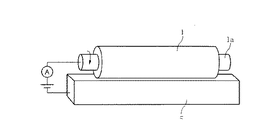
本発明方法においては、具体的には、例えば図1に示すように、軸体1a(芯金)を接地した導電性ロール1に対して平行にアルミニウム等からなる放電用の電極2を配置し、導電性ロール1を一定速度で回転させながら、電源3から電極2に所定の電圧を印加することにより、導電性ロール1にコロナ放電を発生させる。尚、均一な放電を得るためには、例えばガラス管4のような絶縁体を導電性ロール1と電極2との間に設置することが好ましい。
【0016】
本発明で用いるコロナ処理の条件としては、互いに平行に対向させた導電性ロールと電極との距離を0.5〜5.0mm、電極に印加する電圧を0.1〜1.0kWの範囲とし、処理時間を1〜600秒程度とすることが好ましい。導電性ロールと電極との距離が0.5mm未満では、放電による短絡リーク現象が発生し、ロール表面が破壊される。逆に5.0mmを越えると、電圧を高めてもコロナ放電が起こらないからである。また、電極に印加する電圧が0.1kW未満であってもコロナ放電が起こらず、電圧が1.0kWを越えると放電による短絡リーク現象が発生し、ロール表面が破壊される。
【0017】
本発明においては、導電性ロールの表面にコロナ処理を施すことにより、フィルミング現象によるロール表面への付着は発生するものの、付着物が均一に付着するようになる。そのため、付着の進行と共にロールの抵抗値は徐々に増加するが、一本のロール内での抵抗値の均一性は損なわることがない。従って、本発明のコロナ処理した導電性ロールは、帯電ロール、現像ロール、転写ロール等として長期間使用しても、安定した性能を保持し、濃度ムラの無い優れた画像を得ることができる。
【0018】
上記コロナ処理を施すことにより、具体的には、ロールの最大抵抗値(Rmax)と最小抵抗値(Rmin)を対数に換算して、その差(logRmax/Rmin)を桁数で表示したときの値が0.3桁以内となるように、ロール抵抗値を均一化させることができる。コロナ処理によりロールの抵抗値が均一化される理由は明らかではないが、ロール表面全体が適度な粗さになると同時に、表面全体が改質されて適度な反応性を持つようになるため、現像剤や内添剤及び外添剤に由来する付着物がロール表面に均一に付着するためと考えられる。
【0019】
尚、ロール表面への付着の進行によりロール抵抗値は徐々に増加するが、軸体を通してロールに印加する電圧を調整することによって、各ロールに必要な電流値を一定に制御することができる。また、コロナ処理は表面の改質処理であるため、ロールを構成する材料の基本的な特性が損なわれることがない。従って、電気特性の制御などの目的で行うカーボンブラック等の導電性粒子の分散や、耐磨耗性等のロールの材料特性を設定するにあたり、何ら制限を受けることがなく、基本的なロールの構成に関して自由な設計が可能である。
【0020】
本発明に係わる導電性ロールとしては、複写機やプリンター等の電子写真装置に使用される帯電ロール、現像ロール、転写ロール等がある。導電性ロールの構造としては、金属製の軸体(芯金)の外周に少なくとも弾性導電層を設けたものであればよく、例えば弾性導電層の外周に単層又は複数層のゴム層及び/又は樹脂層を設けたロールであってもよい。また、これらの弾性導電層は、ソリッド状であっても、スポンジ(発泡体)状であってもよい。
【0021】
弾性導電層及びその外周に設ける単層又は複数層のゴム層又は樹脂層の材質は特に限定されるものではなく、一般的にロールとして成形可能な材料であればよい。具体的には、ゴム材料としてはウレタンゴム、NBR、SBR、EPDM、CR、シリコンゴム、フッ素ゴム、ヒドリンゴム、IR、BR等を挙げることができ、また樹脂材料としてはウレタン樹脂、アクリル樹脂、ナイロン樹脂、ポリカーボネート樹脂、PVC、PP、フッ素樹脂等を挙げることができる。中でもシリコンゴム、H−NBR、フッ素樹脂は、通常では極めて不均一な付着が起こりやすいので、本発明によるコロナ処理が特に有効である。
【0022】
次に、導電性ロールの成形方法について、簡単に説明する。まず、上下に2分割された金型内に、必要に応じて表面にニッケルメッキ等を施し又は接着剤等を塗布した金属製の軸体(芯金)を配置した後、上記のゴム材料又は樹脂材料を軸体と金型の間の空隙部(キャビティ)内に充填し、必要な時間加熱加圧してロール(弾性導電層)を成形する。ゴム材料や樹脂材料は、溶融状態、有機溶剤等に溶解した溶液状態、コンパウンド等であってよく、その形態は問わない。
【0023】
通常の場合、上記のごとく成形したロールの外周は、円筒研磨等の手法を用いて必要な円筒形状に仕上げる。更に、ロール(弾性導電層)の外周に抵抗調整や保護のための層が必要な場合には、ディッピング法等により所定のゴム材料又は樹脂材料をコーティングし、加熱して単層又は複数層のゴム又は樹脂の層を形成する。尚、複数層を形成する場合は、上記コーティング工程及び加熱工程を複数回繰り返し実施すればよい。
【0024】
【実施例】
試料1〜4の導電性ロールを、以下のようにして作製した。即ち、外径が8mmのSUM22からなる軸体(芯金)の表面に、膜厚4μmの無電解Niメッキを施し、この軸体の外周に型成形により肉厚6mmのNBRからなる弾性導電層を形成し、円筒研磨して試料1のロールとした。また、試料2のロールは、上記試料1のNBRからなる弾性導電層に代えて、型成形により肉厚6mmのSBRからなる弾性導電層を形成してロールとした後、更にその表面にコーティングにより肉厚10μmのナイロン樹脂からなる表層を形成し、円筒研磨した。
【0025】
更に、試料3のロールは、上記試料2と同様に作製したが、弾性導電層を肉厚6mmのシリコンゴムとし、表層は肉厚10μmのH−NBRからなる中間層及び肉厚10μmのフッ素ゴムからなる最表層の複数層とした。試料4では、上記試料2と同様に作製したが、その表層は肉厚10μmのナイロン樹脂からなる内側層と、肉厚100μmのNBRからなる中間層、及び肉厚10μmのナイロン樹脂からなる最表層の複数層とした。
【0026】
上記した試料1〜4の各導電性ロールについて、その構成を下記表1にまとめて、中心の軸体から外側に向かって順に記載した。尚、試料1〜4の各ロールとも、外径は約20mmであって、面長(ゴム部長さ)は300mmとした。
【0027】
【表1】
試料1のロール
軸 体:SUM22(外径8mm、無電解Niメッキ4μm)
弾性層:NBR(肉厚6mm)
試料2のロール
軸 体:SUM22(外径8mm、無電解Niメッキ4μm)
弾性層:SBR(肉厚6mm)
表 層:ナイロン樹脂(肉厚10μm)
試料3のロール
軸 体:SUM22(外径8mm、無電解Niメッキ4μm)
弾性層:シリコンゴム(肉厚6mm)
中間層:H−NBR(肉厚10μm)
最表層:フッ素ゴム(肉厚10μm)
試料4のロール
軸 体:SUM22(外径8mm、無電解Niメッキ4μm)
弾性層:SBR(肉厚6mm)
内側層:ナイロン樹脂(肉厚10μm)
中間層:NBR(肉厚100μm)
最表層:ナイロン樹脂(肉厚10μm)
【0028】
上記試料1〜4の各導電性ロールを、通常のコロナ放電装置を用いてコロナ処理した。即ち、図1に示すように、外側をガラス管4で被覆したアルミニウムの電極2の下方に、電極2とロール表面が平行で且つその間隔が2mmとなるように導電性ロール1を配置し、その導電性ロール1の軸体1aを接地した状態で、軸体1aを駆動して導電性ロール1を20rpmで回転させながら、電極2に出力0.2kWの電圧を印加して60秒間コロナ放電を行った。
【0029】
得られた本発明試料1〜4の各ロールについて、ロールの抵抗値を測定すると共に、ロール内の抵抗値の均一性を評価して、その結果を下記表2に示した。即ち、各ロールの抵抗値の測定は、図2に示すように、金属平板5上に導電性ロール1を乗せ、その軸体1aの両端に各500gfの荷重をかけて導電性ロール1を金属平板5に押しつけた状態で、軸体1aと金属平板5の間にDC100Vを印可し、軸体1aと金属平板5の間に流れる電流量を測定することにより、ロールの抵抗値を求めた。
【0030】
また、1本のロール内での抵抗値の均一性については、図3に示すように、導電性ロール1の外周面に幅12mmの金属ロール6(ベアリング)を100gf荷重で押しつけ、導電性ロール1を回転させた状態で金属ロール6を軸方向に移動させながら、金属ロール6と導電性ロール1の軸体1aの間にDC100Vを印可して、軸体1aと金属ロール6の間に流れる電流量を測定することにより、各ロールの全表面における抵抗値を求めた。このようにして導電性ロール1の全表面について抵抗値を測定し、求めた最大抵抗値Rmaxと最小抵抗値Rminを対数に換算して、その差(logRmax/Rmin)を求めて桁数で表示した。
【0031】
更に、各本発明試料の導電性ロールをレーザービームプリンターの転写ロールとして組み付け、温度30℃、湿度85%の環境下で連続駆動して、実際に10000枚の画像をプリントする耐久試験を行った。この耐久試験終了後の各試料の転写ロールについて、上記と同様にロール抵抗値の測定及び1本のロール内での抵抗値の均一性の評価を行うと共に、ロール表面への付着物の付着状態を観察し、その結果を下記表2に示した。尚、付着状態の評価は、付着物がない又は非常に少ない状態を「付着無し」、付着物があり且つ場所により付着量に差がある状態を「付着ムラ」、及び付着物が全体に均一に付着した状態を「均一付着」と表示した。
【0032】
また、比較例として、前記表1に示す各試料1〜4の構造を有するが、コロナ処理を施していないロールをそれぞれ作製して比較例試料1〜4とし、上記と同様にロール抵抗値の測定、1本のロール内での抵抗値の均一性の評価、及び耐久試験後のロール抵抗値と抵抗値の均一性、並びに付着状態の評価を行い、その結果を表2に併せて示した。
【0033】
【表2】

上記の結果から分るように、いずれの試料のロールも実際に画像をプリントすることによってフィルミング現象によりロール表面への付着が発生し、ロール抵抗値が増加するが、ロール表面にコロナ処理を施した本発明試料の各ロールは抵抗値の均一性が損なわれず、最大抵抗値(Rmax)と最小抵抗値(Rmin)の対数換算値の差(logRmax/Rmin)が好ましいとされる0.3桁以内に維持された。
【0035】
これに対して比較例試料の各ロールでは、付着物がロール表面に不均一に付着し、そのため最大抵抗値(Rmax)と最小抵抗値(Rmin)の対数換算値の差(logRmax/Rmin)が0.8桁以上と極めて大きくなり、抵抗値の均一性を維持することができなかった。
【0036】
また、上記の耐久試験において、実際に10000枚の画像のプリントを行った時点で用紙上に得られた画像を観察評価したところ、本発明試料の各ロールを用いた場合には濃度ムラの無い優れた画像が得られたが、比較例試料の各ロールの場合にはいずれも濃度ムラが認められた。このことから、本発明の導電性ロールを用いることによって、長期間にわたって濃度ムラの無い良好な画像が安定して得られることが分る。
【0037】
【発明の効果】
本発明によれば、コロナ処理という簡単な方法によって、フィルミング現象によるロール表面への付着物がムラ無く均一に付着するようになるため、一本の導電性ロール内での抵抗値の不均一化を無くすことができる。従って、本発明の導電性ロールを電子写真装置の帯電ロール、現像ロール、転写ロール等として使用することによって、濃度ムラのない画像を長期間安定して得ることができる。
【0038】
また、本発明によるコロナ処理はロール表面の改質処理であり、導電性ロールを構成する材料の基本的な特性を損なうことがないため、カーボンブラック等の導電性粒子の分散やロール材料特性を設定するにあたり、何ら制限を受けることがなく、基本的なロールの構成に関して自由な設計が可能である。
【図面の簡単な説明】
【図1】本発明による導電性ロールのコロナ処理を説明するため概念的に図示した概略の斜視図である。
【図2】導電性ロールのロール抵抗値の測定方法を説明するため概念的に図示した概略の斜視図である。
【図3】導電性ロールの抵抗値の均一性を評価するため、ロール全周の抵抗値の測定方法を説明するため概念的に図示した概略の斜視図である。
【符号の説明】
1 導電性ロール
1a 軸体
2 電極
3 電源
4 ガラス管
5 金属平板
6 金属ロール[0001]
[Technical field to which the invention belongs]
The present invention relates to a conductive roll used in a copying machine or a printer using an electrophotographic system, and more particularly to a charging roll, a developing roll, a transfer roll, etc. used around a photosensitive drum.
[0002]
[Prior art]
In general, in an electrophotographic apparatus such as a copying machine or a printer using an electrophotographic system, a conductive roll such as a charging roll, a developing roll, or a transfer roll is disposed around a photosensitive drum on which an electrostatic latent image is formed. ing.
[0003]
The basic structure of these conductive rolls is that an elastic conductive layer made of a rubber elastic body or rubber foam of low hardness is provided on the outer periphery of a metal shaft body (core metal) having conductivity, and if necessary, An intermediate layer and a surface layer for resistance adjustment and the like are sequentially laminated on the outer periphery. In addition, the conductive rolls having such a structure have predetermined electrical characteristics (resistance value and capacitance) in order to transmit the voltage applied to the shaft body to the photosensitive drum.
[0004]
That is, the charging roll controls the chargeability of the photosensitive drum, the developing roll controls the chargeability of the toner and the transferability of the toner (developer) to the photosensitive drum, and the transfer roll moves from the photosensitive drum to the paper or OHP. In order to control the transferability of the toner to the film, it is necessary to equalize the resistance value in each roll while having a predetermined resistance value.
[0005]
Regarding the resistance value of each conductive roll, the target resistance value is made uniform by examining material characteristic design and structural design. Specifically, when conductive particles (generally carbon black) that affect the resistance value are added to each layer of the roll, the type, amount added, dispersibility, etc. are controlled to make the roll resistance value uniform. We are trying to make it. Attempts have also been made to use an ionic conductive agent having better dispersibility than carbon black. From the viewpoint of structural design, a roll structure in which a plurality of layers are laminated and the resistance values are made uniform by combining various resistance values of the laminated layers.
[0006]
In addition, the management range of the resistance value of each conductive roll differs depending on the site where the charging roll, the developing roll, the transfer roll, etc. are used, the usage conditions, and the like. In general, the allowable range for the uniformity of the resistance value is that the maximum resistance value and the minimum resistance value of the roll are measured, and the value obtained by displaying the difference between the logarithm conversion values in the number of digits is within 0.3 digits. It is needed.
[0007]
[Problems to be solved by the invention]
Conductive rolls such as the above-described charging roll, developing roll, and transfer roll always come into contact with toner (developer) when used in combination with a photosensitive drum. In addition to colored particles such as carbon black, various additives are internally or externally added to the developer for the purpose of controlling charging characteristics, releasability, fixability, and the like. So-called filming development in which the polymer of the agent and the developer itself adheres to the roll surface is likely to occur.
[0008]
Specifically, examples of the internal and external additives of the developer include, in addition to general silica, metal oxides such as aluminum oxide and titanium oxide, metal salts such as calcium sulfate and calcium carbonate, stearic acid Fatty acid salts such as zinc are generally used. Since these substances are generally insulative or highly resistant from the purpose of use, the resistance value of the roll increases as the amount of adhesion to the roll surface increases. This increase in resistance value can be compensated for by adjusting the voltage applied to the roll. However, since there is unevenness in the adhesion to the roll surface by filming development, there is a major drawback that the resistance value of the entire roll becomes non-uniform. there were.
[0009]
Such a filming phenomenon is considered to occur depending on molding conditions such as releasability of the material constituting the roll surface itself, distribution of the vulcanization temperature, and the surface condition of the roll. Therefore, conventionally, in order to eliminate the filming phenomenon, the production method has been studied together with the material development. However, with the recent increase in speed and image quality of copying machines and printers, the developer used has been made to have a lower melting point and a smaller diameter, and is more likely to adhere to the roll. For this reason, the unevenness of the deposit tends to increase, and unevenness such as density is more likely to occur in the obtained image.
[0010]
In view of such conventional circumstances, the present invention eliminates uneven adhesion of deposits due to filming development on the surface of a conductive roll such as a charging roll, a developing roll, or a transfer roll, and makes the roll resistance value non-uniform. An object of the present invention is to provide a conductive roll for an electrophotographic apparatus capable of suppressing and obtaining a good image free from density unevenness and a method for producing the same.
[0011]
[Means for Solving the Problems]
In order to achieve the above object, various investigations have been made on the adhesion of the developer and its internal and external additives to the roll surface, but it is difficult to completely prevent adhesion due to the filming phenomenon. It was found that the uniformity of the roll resistance value was not impaired when the kimono adhered uniformly. Further, based on this fact, as a result of examining a method for promoting uniform adhesion to the roll surface, it was found that corona treatment on the roll surface is effective.
[0012]
That is, the present invention is a conductive roll for an electrophotographic apparatus in which at least an elastic conductive layer is provided on the outer periphery of a metal shaft, and the distance between the conductive roll opposed in parallel and the discharge electrode is 0. . 5 to 5. 0 mm, the voltage applied to the discharge electrode is 0. 1~1. 0kW, in which the processing time to provide a conductive roller, characterized in that the corona treatment under conditions of 1 to 600 seconds .
[0014]
DETAILED DESCRIPTION OF THE INVENTION
The corona treatment in the present invention is a local discharge phenomenon that appears when partial dielectric breakdown occurs when a strong unequal electric field is generated around the conductor, and has been conventionally used for the purpose of improving the adhesion of resin materials. Has been.
[0015]
Specifically, in the method of the present invention, for example, as shown in FIG. 1, a
[0016]
The corona treatment conditions used in the present invention are as follows: the distance between the conductive rolls and the electrodes facing each other in parallel is 0.5 to 5.0 mm, and the voltage applied to the electrodes is 0.1 to 1.0 kW. The processing time is preferably about 1 to 600 seconds. If the distance between the conductive roll and the electrode is less than 0.5 mm, a short-circuit leakage phenomenon due to discharge occurs and the roll surface is destroyed. Conversely, if it exceeds 5.0 mm, corona discharge does not occur even if the voltage is increased. Further, even if the voltage applied to the electrode is less than 0.1 kW, corona discharge does not occur. If the voltage exceeds 1.0 kW, a short-circuit leakage phenomenon due to discharge occurs and the roll surface is destroyed.
[0017]
In the present invention, by applying a corona treatment to the surface of the conductive roll, adhesion to the roll surface due to the filming phenomenon occurs, but the deposit is uniformly adhered. Therefore, the resistance value of the roll gradually increases with the progress of adhesion, but the uniformity of the resistance value in one roll is not impaired. Therefore, even if the corona-treated conductive roll of the present invention is used as a charging roll, a developing roll, a transfer roll or the like for a long period of time, it can maintain stable performance and obtain an excellent image without density unevenness.
[0018]
By applying the corona treatment, specifically, the maximum resistance value (Rmax) and minimum resistance value (Rmin) of the roll are converted into logarithms, and the difference (logRmax / Rmin) is displayed in the number of digits. The roll resistance value can be made uniform so that the value is within 0.3 digits. The reason why the roll resistance value is made uniform by corona treatment is not clear, but the entire surface of the roll becomes moderately rough, and at the same time the entire surface is modified to have appropriate reactivity. This is considered to be because the deposits derived from the additive, the internal additive, and the external additive uniformly adhere to the roll surface.
[0019]
Although the roll resistance value gradually increases as the adhesion to the roll surface proceeds, the current value required for each roll can be controlled to be constant by adjusting the voltage applied to the roll through the shaft. Further, since the corona treatment is a surface modification treatment, the basic characteristics of the material constituting the roll are not impaired. Therefore, there is no limitation in setting the material properties of the roll such as the dispersion of conductive particles such as carbon black and the wear resistance for the purpose of controlling electrical characteristics, and the basic roll Free design is possible with regard to configuration.
[0020]
Examples of the conductive roll according to the present invention include a charging roll, a developing roll, and a transfer roll used in electrophotographic apparatuses such as copying machines and printers. The structure of the conductive roll may be any structure as long as at least an elastic conductive layer is provided on the outer periphery of a metal shaft (core metal). For example, a single layer or a plurality of rubber layers on the outer periphery of the elastic conductive layer and / or Or the roll which provided the resin layer may be sufficient. These elastic conductive layers may be solid or sponge (foam).
[0021]
The material of the elastic conductive layer and the single layer or plural rubber layers or resin layers provided on the outer periphery thereof is not particularly limited, and any material can be used as long as it is generally moldable as a roll. Specifically, examples of the rubber material include urethane rubber, NBR, SBR, EPDM, CR, silicon rubber, fluorine rubber, hydrin rubber, IR, BR, and the like, and examples of the resin material include urethane resin, acrylic resin, and nylon. Examples thereof include resins, polycarbonate resins, PVC, PP, and fluororesins. Among them, silicon rubber, H-NBR, and fluororesin are usually very unevenly attached, and the corona treatment according to the present invention is particularly effective.
[0022]
Next, a method for forming the conductive roll will be briefly described. First, after placing a metal shaft body (core metal) whose surface is nickel-plated or coated with an adhesive or the like, if necessary, in a mold that is divided into two parts, one above the other, the rubber material or A resin material is filled in a gap (cavity) between the shaft and the mold, and heated and pressed for a required time to form a roll (elastic conductive layer). The rubber material or the resin material may be in a molten state, a solution state dissolved in an organic solvent or the like, a compound or the like, and its form is not limited.
[0023]
In a normal case, the outer periphery of the roll formed as described above is finished into a necessary cylindrical shape using a technique such as cylindrical polishing. Furthermore, when a layer for resistance adjustment or protection is required on the outer periphery of the roll (elastic conductive layer), a predetermined rubber material or resin material is coated by a dipping method or the like and heated to form a single layer or a plurality of layers. A rubber or resin layer is formed. In addition, what is necessary is just to implement the said coating process and a heating process in multiple times, when forming multiple layers.
[0024]
【Example】
The conductive rolls of Samples 1 to 4 were produced as follows. That is, the surface of a shaft body (core metal) made of SUM22 having an outer diameter of 8 mm is subjected to electroless Ni plating with a film thickness of 4 μm, and the outer periphery of the shaft body is formed by molding and an elastic conductive layer made of NBR with a thickness of 6 mm. Was formed and cylindrically polished to obtain a roll of Sample 1. The roll of
[0025]
Further, the roll of Sample 3 was prepared in the same manner as
[0026]
About each electroconductive roll of above-described samples 1-4, the structure was put together in following Table 1, and it described in order toward the outer side from the center shaft body. Each roll of Samples 1 to 4 had an outer diameter of about 20 mm and a surface length (rubber part length) of 300 mm.
[0027]
[Table 1]
Roll of sample 1 Shaft body: SUM22 (outer diameter 8 mm, electroless Ni plating 4 μm)
Elastic layer: NBR (wall thickness 6mm)
Roll of
Elastic layer: SBR (thickness 6mm)
Surface layer: nylon resin (thickness 10μm)
Roll of sample 3 Shaft body: SUM22 (outer diameter 8 mm, electroless Ni plating 4 μm)
Elastic layer: Silicon rubber (wall thickness 6mm)
Intermediate layer: H-NBR (thickness 10 μm)
Outermost layer: fluororubber (thickness 10μm)
Roll of sample 4 Shaft body: SUM22 (outer diameter 8 mm, electroless Ni plating 4 μm)
Elastic layer: SBR (thickness 6mm)
Inner layer: nylon resin (thickness 10μm)
Intermediate layer: NBR (thickness 100 μm)
Outermost layer: nylon resin (thickness 10μm)
[0028]
Each electroconductive roll of the said samples 1-4 was corona-treated using the normal corona discharge device. That is, as shown in FIG. 1, the conductive roll 1 is arranged below the
[0029]
About each roll of the obtained this invention samples 1-4, while measuring the resistance value of a roll, the uniformity of the resistance value in a roll was evaluated, and the result was shown in following Table 2. That is, as shown in FIG. 2, the resistance value of each roll is measured by placing the conductive roll 1 on a metal flat plate 5 and applying a load of 500 gf to both ends of the shaft body 1a. While being pressed against the flat plate 5, DC 100 V was applied between the shaft body 1 a and the metal flat plate 5, and the amount of current flowing between the shaft body 1 a and the metal flat plate 5 was measured to obtain the resistance value of the roll.
[0030]
As for the uniformity of the resistance value in one roll, as shown in FIG. 3, a metal roll 6 (bearing) having a width of 12 mm is pressed against the outer peripheral surface of the conductive roll 1 with a load of 100 gf. DC 100V is applied between the metal roll 6 and the shaft body 1a of the conductive roll 1 while the metal roll 6 is moved in the axial direction while rotating 1 and flows between the shaft body 1a and the metal roll 6. By measuring the amount of current, the resistance value on the entire surface of each roll was determined. In this way, the resistance value is measured for the entire surface of the conductive roll 1, the maximum resistance value Rmax and the minimum resistance value Rmin thus obtained are converted into logarithms, and the difference (logRmax / Rmin) is obtained and displayed in digits. did.
[0031]
Furthermore, a durability test was performed in which the conductive roll of each sample of the present invention was assembled as a transfer roll of a laser beam printer, and was continuously driven in an environment of a temperature of 30 ° C. and a humidity of 85% to actually print 10,000 images. . Regarding the transfer roll of each sample after the end of the durability test, the roll resistance value is measured and the uniformity of the resistance value in one roll is evaluated in the same manner as described above, and the adhesion state of the deposit on the roll surface is measured. The results are shown in Table 2 below. In addition, the evaluation of the adhesion state is “no adhesion” when there is no or very little adhesion, “adhesion unevenness” when there is an adhesion and there is a difference in the amount of adhesion depending on the location, and the adhesion is uniform throughout. The state of adhering to was indicated as “uniform adhesion”.
[0032]
Moreover, as a comparative example, it has the structure of each sample 1-4 shown in the said Table 1, However, The roll which has not performed the corona treatment is each produced as comparative example sample 1-4, and roll resistance value is the same as the above Measurement, evaluation of uniformity of resistance value in one roll, evaluation of uniformity of roll resistance value and resistance value after endurance test, and adhesion state, and the results are also shown in Table 2. .
[0033]
[Table 2]
As can be seen from the above results, every sample roll actually prints an image, which causes filming to adhere to the roll surface and increases the roll resistance value. Each roll of the applied inventive sample does not impair the uniformity of the resistance value, and the difference between the maximum resistance value (Rmax) and the minimum resistance value (Rmin) in logarithmically converted value (logRmax / Rmin) is preferably 0.3. Maintained within digits.
[0035]
On the other hand, in each roll of the comparative sample, deposits adhered non-uniformly to the roll surface, so that the difference (logRmax / Rmin) between the logarithmically converted values of the maximum resistance value (Rmax) and the minimum resistance value (Rmin) is It became extremely large with 0.8 digits or more, and the uniformity of the resistance value could not be maintained.
[0036]
Further, in the above durability test, when the image obtained on the sheet was actually observed and evaluated when 10,000 images were actually printed, there was no density unevenness when each roll of the sample of the present invention was used. Although an excellent image was obtained, density unevenness was observed in each of the rolls of the comparative sample. From this, it can be seen that by using the conductive roll of the present invention, a good image without density unevenness can be stably obtained over a long period of time.
[0037]
【The invention's effect】
According to the present invention, since the deposit on the roll surface due to the filming phenomenon is uniformly adhered by a simple method called corona treatment, the resistance value is not uniform within one conductive roll. Can be eliminated. Therefore, by using the conductive roll of the present invention as a charging roll, a developing roll, a transfer roll or the like of an electrophotographic apparatus, an image having no density unevenness can be stably obtained for a long period of time.
[0038]
In addition, the corona treatment according to the present invention is a roll surface modification treatment and does not impair the basic characteristics of the material constituting the conductive roll. Therefore, the dispersion of conductive particles such as carbon black and the roll material characteristics can be improved. There are no restrictions on the setting, and a free design is possible with respect to the basic roll configuration.
[Brief description of the drawings]
FIG. 1 is a schematic perspective view conceptually illustrated for explaining corona treatment of a conductive roll according to the present invention.
FIG. 2 is a schematic perspective view conceptually illustrated for explaining a method of measuring a roll resistance value of a conductive roll.
FIG. 3 is a schematic perspective view conceptually illustrated for explaining a method of measuring the resistance value of the entire circumference of the roll in order to evaluate the uniformity of the resistance value of the conductive roll.
[Explanation of symbols]
DESCRIPTION OF SYMBOLS 1 Conductive roll
Claims (1)
Priority Applications (3)
| Application Number | Priority Date | Filing Date | Title |
|---|---|---|---|
| JP2000228589A JP3760735B2 (en) | 2000-07-28 | 2000-07-28 | Conductive roll |
| EP01118140A EP1176476A2 (en) | 2000-07-28 | 2001-07-26 | Conductive roll and manufacturing method thereof |
| US09/915,356 US20020035020A1 (en) | 2000-07-28 | 2001-07-27 | Conductive roll and manufacturing method thereof |
Applications Claiming Priority (1)
| Application Number | Priority Date | Filing Date | Title |
|---|---|---|---|
| JP2000228589A JP3760735B2 (en) | 2000-07-28 | 2000-07-28 | Conductive roll |
Publications (2)
| Publication Number | Publication Date |
|---|---|
| JP2002040759A JP2002040759A (en) | 2002-02-06 |
| JP3760735B2 true JP3760735B2 (en) | 2006-03-29 |
Family
ID=18721841
Family Applications (1)
| Application Number | Title | Priority Date | Filing Date |
|---|---|---|---|
| JP2000228589A Expired - Lifetime JP3760735B2 (en) | 2000-07-28 | 2000-07-28 | Conductive roll |
Country Status (3)
| Country | Link |
|---|---|
| US (1) | US20020035020A1 (en) |
| EP (1) | EP1176476A2 (en) |
| JP (1) | JP3760735B2 (en) |
Families Citing this family (5)
| Publication number | Priority date | Publication date | Assignee | Title |
|---|---|---|---|---|
| US8376922B2 (en) * | 2004-06-09 | 2013-02-19 | Bridgestone Corporation | Developing roller, charging roller, conductive roller and method for producing the same |
| JP2007298775A (en) | 2006-04-28 | 2007-11-15 | Sharp Corp | Image forming apparatus, charging roller, and method and device for manufacturing charging roller |
| JP4653204B2 (en) * | 2008-09-16 | 2011-03-16 | 住友ゴム工業株式会社 | Conductive roll |
| JP4739463B1 (en) | 2009-12-21 | 2011-08-03 | キヤノン株式会社 | Method for manufacturing electrophotographic roller |
| JP5730112B2 (en) * | 2011-04-20 | 2015-06-03 | キヤノン株式会社 | Method for manufacturing electrophotographic roller |
-
2000
- 2000-07-28 JP JP2000228589A patent/JP3760735B2/en not_active Expired - Lifetime
-
2001
- 2001-07-26 EP EP01118140A patent/EP1176476A2/en not_active Withdrawn
- 2001-07-27 US US09/915,356 patent/US20020035020A1/en not_active Abandoned
Also Published As
| Publication number | Publication date |
|---|---|
| EP1176476A2 (en) | 2002-01-30 |
| US20020035020A1 (en) | 2002-03-21 |
| JP2002040759A (en) | 2002-02-06 |
Similar Documents
| Publication | Publication Date | Title |
|---|---|---|
| JP7394928B2 (en) | charging roll | |
| JP7342209B2 (en) | charging roll | |
| JP2008209488A (en) | Charging device, process cartridge and image forming apparatus | |
| JP3760735B2 (en) | Conductive roll | |
| JPH01142569A (en) | Electroconductive roll | |
| JP3796400B2 (en) | Conductive member, process cartridge, and image forming apparatus | |
| JP4248711B2 (en) | Polyimide tubular material and manufacturing method thereof | |
| JP2004037551A (en) | Developing roller and developing apparatus equipped with the same | |
| JP3646753B2 (en) | Semiconductive member | |
| JP2013088681A (en) | Inspection method and manufacturing method for roller for developing device | |
| JP2003207967A (en) | Roller for electrophotography and image forming apparatus | |
| CN115997175A (en) | Conductive roller, image forming apparatus, and detection method for conductive roller | |
| JP2003207966A (en) | Member for electrophotography and image forming apparatus | |
| JPH08190263A (en) | Developing roll | |
| JP4765549B2 (en) | Transfer roll and image forming apparatus | |
| JP2000206779A (en) | Toner carrier and image forming device | |
| JP7342136B2 (en) | charging roll | |
| JP4289928B2 (en) | Method for manufacturing conductive member | |
| JP4233691B2 (en) | Developer carrying member and image forming apparatus | |
| JP2000206778A (en) | Toner carrier and image forming device | |
| JP2002040802A (en) | Developing roller and developing device | |
| JP2024013026A (en) | Conductive roller, manufacturing method of the same, process cartridge for electrophotography using the conductive roller and electro-photographic image formation apparatus | |
| JP3246702B2 (en) | Contact type charging member | |
| JPH09179379A (en) | Electrically conductive roll | |
| JPH08286393A (en) | Electrophotographic device |
Legal Events
| Date | Code | Title | Description |
|---|---|---|---|
| A621 | Written request for application examination |
Free format text: JAPANESE INTERMEDIATE CODE: A621 Effective date: 20040127 |
|
| A977 | Report on retrieval |
Free format text: JAPANESE INTERMEDIATE CODE: A971007 Effective date: 20050609 |
|
| A131 | Notification of reasons for refusal |
Free format text: JAPANESE INTERMEDIATE CODE: A131 Effective date: 20050614 |
|
| A131 | Notification of reasons for refusal |
Free format text: JAPANESE INTERMEDIATE CODE: A131 Effective date: 20050830 |
|
| A521 | Request for written amendment filed |
Free format text: JAPANESE INTERMEDIATE CODE: A523 Effective date: 20051024 |
|
| A131 | Notification of reasons for refusal |
Free format text: JAPANESE INTERMEDIATE CODE: A131 Effective date: 20051122 |
|
| A521 | Request for written amendment filed |
Free format text: JAPANESE INTERMEDIATE CODE: A523 Effective date: 20051124 |
|
| TRDD | Decision of grant or rejection written | ||
| A01 | Written decision to grant a patent or to grant a registration (utility model) |
Free format text: JAPANESE INTERMEDIATE CODE: A01 Effective date: 20051220 |
|
| A61 | First payment of annual fees (during grant procedure) |
Free format text: JAPANESE INTERMEDIATE CODE: A61 Effective date: 20060102 |
|
| R150 | Certificate of patent or registration of utility model |
Free format text: JAPANESE INTERMEDIATE CODE: R150 Ref document number: 3760735 Country of ref document: JP Free format text: JAPANESE INTERMEDIATE CODE: R150 |
|
| FPAY | Renewal fee payment (event date is renewal date of database) |
Free format text: PAYMENT UNTIL: 20100120 Year of fee payment: 4 |
|
| FPAY | Renewal fee payment (event date is renewal date of database) |
Free format text: PAYMENT UNTIL: 20110120 Year of fee payment: 5 |
|
| FPAY | Renewal fee payment (event date is renewal date of database) |
Free format text: PAYMENT UNTIL: 20120120 Year of fee payment: 6 |
|
| FPAY | Renewal fee payment (event date is renewal date of database) |
Free format text: PAYMENT UNTIL: 20130120 Year of fee payment: 7 |
|
| FPAY | Renewal fee payment (event date is renewal date of database) |
Free format text: PAYMENT UNTIL: 20130120 Year of fee payment: 7 |
|
| EXPY | Cancellation because of completion of term |