JP3752981B2 - Optical signal transmission device, optical data bus system, and signal processing device - Google Patents
Optical signal transmission device, optical data bus system, and signal processing device Download PDFInfo
- Publication number
- JP3752981B2 JP3752981B2 JP2000252661A JP2000252661A JP3752981B2 JP 3752981 B2 JP3752981 B2 JP 3752981B2 JP 2000252661 A JP2000252661 A JP 2000252661A JP 2000252661 A JP2000252661 A JP 2000252661A JP 3752981 B2 JP3752981 B2 JP 3752981B2
- Authority
- JP
- Japan
- Prior art keywords
- incident
- optical signal
- signal transmission
- transmission device
- optical
- Prior art date
- Legal status (The legal status is an assumption and is not a legal conclusion. Google has not performed a legal analysis and makes no representation as to the accuracy of the status listed.)
- Expired - Fee Related
Links
Images


Description
【0001】
【発明の属する技術分野】
本発明は、光信号伝達装置、光データバスシステム、及び信号処理装置に係り、より詳しくは、入射された光信号を複数に分岐した状態で出射する光信号伝達装置、該光信号伝達装置を用いた光データバスシステム、及び信号処理装置に関する。
【0002】
【従来の技術】
超大規模集積回路(VLSI)の開発により、データ処理システムで使用する回路基板(ドーターボード)の回路機能が大幅に増大してきている。回路機能が増大するにつれて各回路基板に対する信号接続数が増大する為、各回路基板(ドーターボード)間をバス構造で接続するデータバスボード(マザーボード)には多数の接続コネクタと接続線を必要とする並列アーキテクチャが採用されている。接続線の多層化と微細化により並列化を進めることにより並列バスの動作速度の向上が計られてきたが、接続配線間容量や接続配線抵抗に起因する信号遅延により、システムの処理速度が並列バスの動作速度によって制限されることもある。また、並列バス接続配線の高密度化による電磁ノイズ(EMI:Electromagnetic Interference)の問題もシステムの処理速度向上に対しては大きな制約となる。
【0003】
この様な問題を解決し並列バスの動作速度の向上を計る為に、光インターコネクションと呼ばれるシステム内光接続技術を用いることが検討されている。光インターコネクション技術の概要は、内田,回路実装学術講演大会 15C01,p.201〜202やH.Tomimuro et al, IEEE Tokyo Section Denshi Tokyo No.33 p.81〜86(1994)に記載されている様に、システムの構成内容により様々な形態が提案されている。
【0004】
従来提案された様々な形態の光インターコネクション技術のうち、特開平2-41042号公報には発光/受光デバイスを用いた光データ伝送方式が考案されている。特開平2-41042号公報では、各回路基板の表裏両面に発光/受光デバイスを配置し、システムフレームに組み込まれた隣接する回路基板上の発光/受光デバイス間を空間的に光で結合した、各回路基板相互間のループ伝送用の直列光データ・バスが提案されている。この方式では、ある1枚の回路基板から送られた光信号が隣接する回路基板で光/電気変換され、さらにその回路基板でもう一度電気/光変換されて、次に隣接する回路基板に光信号を送るというように、各回路基板が順次直列に配列され各回路基板上で光電気変換、電気/光変換を繰り返しながらシステムフレームに組み込まれたすべての回路基板間に伝達される。この為、信号伝達速度は各回路基板上に配置された受光/発光デバイスの光/電気変換・電気/光変換速度に依存すると同時にその制約を受ける。また、各回路基板相互間のデータ伝送には、各回路基板上に配置された受光/発光デバイスによる、自由空間を介在させた光結合を用いている為、隣接する光データ伝送路間の干渉(クロストーク)が発生しデータの伝送不良が予想される。また、システムフレーム内の環境、例えば埃などにより光信号が散乱することによりデータの伝送不良が発生することも予想される。
【0005】
特開昭61-196210号公報では、プレート表面に配置された回折格子、反射素子により構成された光路を介して回路基板間を光学的に結合する方式が考案されている。この方式では、1点から発せられた光を固定された1点にしか接続できないために、電気バスの様に全ての回路ボード間を網羅的に接続することができない。
【0006】
また、分岐素子を具備した光接続装置を使用した各回路基板相互間のデータ伝送に関しても、いくつかの特許が考案されている。
【0007】
特開昭58-42333号公報では、ハーフミラーを複数使用した回路基板相互間のデータ伝送の例が示されている。しかしながら、ハーフミラーを複数用いた場合、装置が大型化し、各ミラー毎に発光/受光デバイスとの光学的位置合わせが必要となる。また、ハーフミラーを通過した伝送光は、入射に対してほぼ半分の光強度となるため、複数回、分岐・伝送を繰り返すと光強度が微弱となり、受光デバイスでの十分な光強度が得られなくなり、信号伝送が不可能になるという問題がある。
【0008】
特開平4-134415号公報では、複数個のレンズが形成されたレンズアレイの側面より、光信号を入射し、各々のレンズより、出射する方式が考案されている。この方式では、光の入射位置に近いレンズほど、出射光量が大きくなる為に入射位置と出射位置との位置関係により出射信号の強度のバラツキが懸念される。また、側面から入射した光が対向する側面から抜けてしまう割り合いも高い為、入射光量の利用効率も低い。
【0009】
また、分岐比率を入力端から順次大きくすることで、ほぼ均等な光信号が伝送できる光ファイバを使った光バス方式が、特開昭63-1223号公報に開示されている。このような方式に適応可能なカプラの形成方法が、IEEE Photonics Technology Letters,vol.8,No.12,December (1996)に述べられている。ここに示されているカプラの形成方法は、光ファイバに形成されたV溝により、分岐を行うものである。V溝のサイズを調整することで、出力光量の調整は、可能と考えられるが作製は非常に困難であり入射光量の利用効率も低い。
【0010】
また、分岐された光信号の強度を均一化するスターカプラが、特開平9-184941号公報に開示されている。このスターカプラは、概略的には、複数の光ファイバの片端を束ねて固定し、その一方の端面に複数の光ファイバを覆う広さの導光路を当接し、他方の端面に光反射手段を備えている。
【0011】
このようなカプラを用いて回路基板相互間のデータ伝送を行う場合、接続基板数が多くなると受発光素子と接続するファイバの本数が多くなり、構成が複雑になり、装置が大型化するという問題が生じる。
【0012】
【発明が解決しようとする課題】
本発明は、上記事情に鑑み、構成が容易な光信号伝達装置、その光信号伝達装置を複数用いた光データバスシステム、及びその光データバスを備えたデータの送受を含む信号処理を行なう信号処理装置を提供することを目的とする。
【0013】
【課題を解決するための手段】
上記目的達成のため本発明は、一端に複数の段差を設けることにより形成された、光信号を入射又は出射若しくは入射及び出射するための複数の入出射部を有する透光性媒体と、前記透光性媒体の他端に配置され、前記入出射部から入射された光信号を、前記複数の入出射部方向に反射する反射手段と、を備えた光信号伝達装置を提供する。
【0014】
即ち、透光性媒体の一端には、複数の段差を設けることにより、入出射部が形成されている。なお、複数の入出射部は、透光性媒体の一端に複数の段差を階段状に設けることにより形成する。透光性媒体の他端には、入出射部から入射された光信号を、複数の入出射部方向に反射する反射手段が設けられている。
【0015】
よって、複数の入出射部の内の1つの入出射部から光信号が入射された場合、該光信号は透光性媒体を透過して反射手段に到達する。反射手段に到達した光信号は、複数の入出射部方向に反射される。
【0016】
そして、本発明では、透光性媒体の側面は、反射手段により反射された光信号の内、入出射部に直接入射する光信号以外の光信号を、入出射部に導くように反射する。
【0017】
反射手段により反射された光信号の内、入出射部に直接入射する光信号ばかりでなく該直接入射する光信号以外の光信号も、入出射部に導くように反射するので、光の利用効率を高くすることができる。
【0018】
ここで、透光性媒体の一端に形成された複数の段差各々の段差長を等しくしてもよい。また、複数の段差各々の段差長さをL1、透光性媒体の他端から該他端に最接近する位置に位置する入出射部までの長さをL2とした場合、透光性媒体に、L2≧L1を満足するように、複数の段差を設けてもよい。
【0019】
また、透光性媒体の入出射部は、入射された光信号を反射手段の方向に反射しかつ反射手段及び前記側面から反射された光信号を、入射方向と反対方向に反射するようにしてもよい。このような場合、入出射部となる透光性媒体の面は、透光性媒体の上面に対して45°となるように形成される。入出射部となる面は全反射面となるように設定するのが望ましい。そして、複数の入出射部の少なくとも1つは他の入出射部の反射方向と異なる方向に光信号を反射するようにしてもよい。
【0020】
また、透光性媒体の側面は、反射手段により反射された光信号の内、入出射部に直接入射する光信号以外の光信号を、複数の入出射部全域に導くように反射するようにしてもよい。
【0021】
例えば、透光性媒体は、光拡散手段の拡散角を2θ、光拡散手段から前記拡散手段に最接近する入出射部を見た最大の見込み角を2θ′とした場合、tanθ≧tan3θ′の関係を満たすように、構成してもよい。また、透光性媒体は、光拡散手段の拡散角を2θ、透光性媒体の開口数をsinφとした場合、θ≦φの関係を満たすように、構成してもよい。
【0022】
このように、反射手段により反射された光信号の内、入出射部に直接入射する光信号以外の光信号を、複数の入出射部全域に導くように反射するので、より光の利用効率を向上させることができる。
【0023】
上記反射手段は、入出射部から入射される光信号を、複数の入出射部方向に拡散反射してもよいし、鏡面反射してもよい。
【0024】
また、透光性媒体は、一端に複数の段差を設けることにより入出射部が形成されているため、複数の回路基板を互いに平行に、透光性媒体の上部に立設することで、回路基板上に設けられている入出射手段である受発光素子を入出射部に対向して配置することが可能となり、これにより構成を容易にすることができる。
【0025】
さらに、本発明の光信号伝達装置を用いて、光信号によりデータを伝送する光データバスシステムを構成することが可能となる。
【0026】
このとき、複数の入出射部の一部に外部機器との光接続用に光ファイバを接続し、その接続部をコネクタとして構成してもよい。あるいは、入出射部の一部に外部機器との接続用のコネクタを設けてもよい。
【0027】
また、本発明の光信号伝達装置と、入出射部に対向して配置され、光信号を入出射する入出射手段を有する回路基板とを備えた信号処理装置が提案される。即ち、データを担持する光信号を、入出射手段を用いて入出射部に入射すると、前述したように光信号を分岐して、複数の入出射部を介して外部に出射する。なお、入出射手段としては、発光素子、受光素子を用いることができるが、入出射部各々に対して発光素子、受光素子を双方設けてもよいし、個別に設けてもよい。
【0028】
【発明の実施の形態】
以下、図面を参照して、本発明の実施の形態について説明する。
【0029】
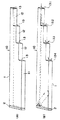
〔第1の実施の形態〕
図1(A)は、本実施の形態に係る光信号伝達装置10の概略構成図を示している。光信号伝達装置10は、階段状の段差12が複数(本実施の形態では3つ)形成された直方体形状の透光性媒体1を備えている。透光性媒体1の一方の端面には反射型光拡散層2が配置されている。また、透光性媒体1の他方の端面(段差12によって特定される複数の端面)13は、入出射部として機能する。
【0030】
次に、図1(B)を参照して、本実施の形態に係る光信号伝達装置10の入力光の分岐方法について説明する。
【0031】
複数の入出射部13のうち、入出射部131より入射し、入出射部131、132、133、134より出射する場合について説明する。入出射部131より入射した光(例えばコリメートされたレーザ光)は、透光性媒体1内を直進し、反射型光拡散層2に到達し上下方向(透光性媒体1の厚さ方向)及び左右方向(透光性媒体1の幅方向)に拡散反射される。拡散反射された拡散光は、透光性媒体1内を側面で反射されながら伝搬し、入出射部131、132、133、134全域へと導かれ出射される。なお、拡散反射された拡散光は、透光性媒体1の側面で反射された拡散光が含まれるため、複数の入出射部(131、132、133、134)に直接入射する拡散光のみではない。
【0032】
ここで、本実施の形態では、透光性媒体1は、側面が複数の入出射部(131、132、133、134)に直接入射する光信号以外の光信号を入出射部全域に反射するように、構成している。
【0033】
即ち、反射型光拡散層2によって拡散反射された拡散光が透光性媒体1の幅よりも大きく広がる場合には、拡散光は、少なくとも1回は透光性媒体1の側面で全反射される。従って、反射型光拡散層2によって拡散反射された、拡散光の左右方向への広がり角を適宜選択することによって入出射部131、132、133、134へと導かれる出射光強度を均一にすることが可能となる。
【0034】
特に、本実施の形態では、光信号伝達装置10を、図11(A)、図11(B)に示すように、透光性媒体1の反射型光拡散層2が配置されている端面に最も近い端部13(135)が形成された位置までの最大の見込み角を2θ’、反射光拡散層2の拡散特性における広がり角(左右方向)を2θとした場合に、tanθ≧3tanθ’の関係を満たすように、構成している。
【0035】
このようにtanθ≧3tanθ’とすることにより、反射型光拡散層2により左右に拡散された拡散光信号は、少なくとも1回は透光性媒体1の側面で全反射され、透光性媒体1の他方の端面、即ち入出射部を有する面に導かれる。tanθ<3tanθ’の場合は、中心での出射光強度が大きく、周辺の出射光強度が小さくなり、出射光強度の均一性が悪くなる。これに対して、tanθ=3tanθ’の場合には、図11(B)に示すように拡散光信号(直接入射光)と左右の側面で全反射した拡散光信号(全反射入射光)が重ね合わせられ、出射光強度の均一性を向上させることが可能となる。
【0036】
また、拡散反射部の拡散特性における広がり角を2θ、透光性媒体の開口数をsinφとした場合、θ≦φの関係を満たすこと、即ち、拡散光信号の透光性媒体1の上下面への入射角を臨界角以上にすることができ、拡散光を外部に放出せず、拡散光信号の全てを透光性媒体1の上下面で全反射させて利用できる為、光信号の利用効率を上げることが可能となる。
【0037】
以上説明したように本実施の形態の光信号伝達装置によれば、入射光信号の利用効率を向上させると共に均等な光分岐が可能となり、出射部における出力レベルを均一にすることが可能となる。
【0038】
以上説明した実施の形態では、4つ(図11では5つ)の入出射部13を有する光信号伝達装置10について示したが、入出射部13の数は、これに限らずさらに複数形成することが可能である。
【0039】
また、入力の際、コリメートされたレーザ光が、透光性媒体1内を直進せず、内部で全反射しながら、反射型光拡散層2に到達する場合や、入射光に広がりがあり透光性媒体1内を全反射しながら、反射型光拡散層2に到達する場合においても、ほぼ同等な出射光強度が得られる。
【0040】
さらに、透光性媒体1の上下面及び左右の側面(幅方向奥側及び手前側の側面)には、透光性媒体1よりも屈折率の小さいクラッド層(図示せず)を配置することも可能である。これにより、クラッド層に包囲された透光性媒体1は、導光路を形成するコア部として機能する。透光性媒体1には、ポリメチルメタクリレート、ポリカーボネート、アモルファスポリオレフィンのようなプラスチック材料又は無機ガラス等を用いることが可能であり、階段状の段差は研削により加工を行うことによって形成される。また、プラスチック材料の場合、射出成型等の方法でも作製可能である。
【0041】
反射型光拡散層2としては、例えばビーム整形ディヒューザ:LSD(Physical Optics Corporation製)を用い、透光性媒体1に対して、拡散光の厚さ方向の広がり角と幅方向の広がり角の制御を行う。透過型LSDは、ポリカーボネート等の透明基板材料に配置されたエポキシ層に、入射光に対して所定の拡散角に拡散させるホログラム面を転写して形成される。反射型LSDは、反射基板(例えばAlが着膜された透明基板)のエポキシ層に、入射光に対して所定の拡散角に拡散させるホログラム面を転写して形成または、透過型LSDに直接Al等の反射面を着膜し形成する。
【0042】
〔第2の実施の形態〕
次に、本発明の第2の実施の形態を説明する。本実施の形態では、前述した第1の実施の形態と同様の構成部分があるので、同一部分には同一の符号を付してその説明を省略し、異なる部分を説明する。
【0043】
図2(A)は、本実施の形態に係る光信号伝達装置10の概略構成を示している。第2実施の形態において、第1実施の形態との違いは、第1実施の形態における入出射部13に対応する入出射部14の面が透光性媒体1の上面に対して45°に形成されていることである。従って第2実施の形態では、透光性媒体1に対して、垂直方向(上面方向)に光の入出射を行うことができる。
【0044】
次に、図2(B)を参照して、本実施の形態に係る光信号伝達装置10の入力光の分岐方法について説明する。
【0045】
ここでは、複数の入出射部(全反射面)14のうち、例えば、入出射部141より入射し、入出射部141、142、143、144より出射する場合について示す。入射光(例えばコリメートされたレーザ光)は、入出射部141で全反射され、透光性媒体1内を直進し、反射型光拡散層2に到達し上下方向及び左右方向に拡散反射される。
【0046】
なお、拡散反射された拡散光は、透光性媒体1内を側面で反射されながら伝搬し、入出射部141、142、143、144全域へと導かれ、入出射部141、142、143、144で再び全反射されて、出射される。出射光強度を均一にできる機能は、第1実施の形態と同様である。
【0047】
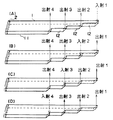
入出射方向は、垂直方向(上面方向)に限らず、垂直方向(下面方向)及び、幅方向(左右方向)でもよく、入出射部の面の形成方向により、入出射方向の変更は可能である。例えば、図3(A)〜図3(D)に示すように、種々の入出射方向を組み合わせることも可能である。
【0048】
図3(A)及び図3(B)には、同じ形態の透光性媒体1が示されており、図3(B)には、図3(A)に示される透光性媒体1に対する光信号の入出射の方向が示されている(入出射部142から入射)。即ち、入出射部141、143は、下面方向入射、上面方向出射するように、透光性媒体1の上面に対して45°に面が形成されており、入出射部142、144は、上面方向入射、下面方向出射するように、透光性媒体1の下面に対して45°に面が形成されている。
【0049】
図3(C)及び図3(D)には、同じ形態の透光性媒体1が示されており、図3(D)には、図3(C)に示される透光性媒体1に対する光信号の入出射の方向が示されている。即ち、入出射部141は、左方向入射、右方向出射となるように、透光性媒体1の奥側側面に対して45°に面が形成されており、入出射部142は、上面方向入射、下面方向出射となるように、透光性媒体1の下面に対して45°に面が形成されており、入出射部143は、下面方向入射、上面方向出射となるように、透光性媒体1の上面に対して45°に面が形成されており、入出射部144は、右方向入射、左方向出射するように、透光性媒体1の手前側側面に45°で面が形成されている。
【0050】
図5、図6は、図4(A)〜図4(D)にも示すように、第2実施の形態において、透光性媒体1の全長H1が45mm、幅H2が4mm、厚さH3が1mm、反射型光拡散層2が配置されている端面から最も近い入出射部144までの距離H4である11が30mm、階段状の段差12の長さH5が5mmで、反射型光拡散層2として、ホログラム形成面の反対面(LSDの基板裏面)に反射層としてAlをスパッタしたLSD 0.2×40PC−8(拡散光の厚さ方向の広がり角が0.2°、幅方向の広がり角が40°)を用いた場合の、各入出射部13から出力される出射光効率と出射光強度の均一性を示している。
【0051】
図5に示すように、何れの入出射部から入射(入射1〜4)しても、各入出射部での出射光の効率は、およそ18%である。また、図6に示すように、各入出射部での出射光強度の均一性(((最大効率―最小効率)/(最大効率+最小効率))×100[%])は、およそ4%と非常に良好な値が得られている。
【0052】
尚、光源としては680nmの波長を有する光を発する端面発光型のレーザダイオードを用いている。
【0053】
更に、図8〜図10は、透光性媒体1の幅が4mmで、厚さ1mmのとき、反射型光拡散層2が配置されている端面から、最も近い入出射部144までの距離11(L2)と段差長12(L1)を変化させた場合の光線追跡シミュレーションにおける出射光強度の均一性を示している。図8〜図10から理解できるように、L2が短くなる程(L2が40→10)、また、L1が長くなる程(L1が15→25)、均一性が悪くなる傾向を示している。そして、シミュレーション結果から、L2をL1以上、より好ましくは、2倍程度以上にすることで、出射光強度の均一性は、10%以下が達成可能であることが理解できる。上記第1の実施の形態及び第2の実施の形態は、この結果に基づいて、長さを決めて、形状を決定している。
【0054】
〔第3の実施の形態〕
次に、本発明の第3の実施の形態を説明する。本実施の形態では、前述した第1及び第2の実施の形態と同様であるので、同一部分には同一の符号を付してその説明を省略する。
【0055】
図12(A)は、本実施の形態に係る光信号伝達装置10の概略構成を示している。光信号伝達装置10は、階段状の段差12が複数(本実施の形態では3つ)形成された直方体状の透光性媒体1を備えている。段差12によって特定される複数の端面は、入出射部131、132、133、134として機能する。透光性媒体1の複数の端面に対向する端面には、Al等の鏡面反射を可能とする材質によって、入出射部131、132、133、134の各々に対応した複数(本実施の形態では4つ)の光反射層4が形成されている。光信号伝達装置10に対する入出射部131、132、133、134の位置が各々異なっているので、各光反射層4の角度は、反射された光信号が入出射部全域に向かうように設定されている。
【0056】
図12(B)は、図12(A)に示される入出射部131、132、133、134の各々に相当する入出射部141、142、143、144の各々の面が透光性媒体1の上面に対して45°に形成されている光信号伝達装置10を示す。図12(A)に示される光信号伝達装置10では、透光性媒体1に対して水平方向(長手方向)に光の入出射を行うが、図12(B)に示される光信号伝達装置10では、透光性媒体1に対して上下方向(厚さ方向)に光の入出射を行う。
【0057】
次に、本実施の形態に係る光信号伝達装置10の入力光の分岐方法について説明する。図12(A)において、複数の入出射部13のうち、例えば、入出射部131より入射し、入出射部131、132、133、134より出射する場合について示す。入出射部131より入射した光(例えばレーザダイオードより放射された光)は、透光性媒体1内を直進し、光反射層4に到達する。通常、レーザ光は放射角(厚さ方向(θ1)、幅方向(θ2))で放射される。レーザ光が光反射層4に到達すると、光反射層でθ1(厚さ方向)、θ2(幅方向)の広がり角で反射される。(但し、入出射部で全ての入射光が反射されたとする。)
【0058】
反射されたレーザ光は、透光性媒体1内を側面で反射されながら伝搬され、入出射部131、132、133、134全域へと導かれ、出射される。なお、入出射部131、132、133、134に直接入射する光のみではなく、入出射部に導かれる光は、透光性媒体1の側面で反射された光が含まれる。
【0059】
このため、光反射層4によって反射される光が透光性媒体1の幅よりも大きく広がる場合には、少なくとも1回は透光性媒体1の側面でレーザ光が全反射される。従って、光反射層4によって反射された、光の左右方向への広がり角(レーザダイオードの放射角で規定される)を適宜選択することによって、入出射部131、132、133、134へと導かれる出射光強度を均一にすることが可能となる。
【0060】
以上、説明した本実施の形態では、4つの入出射部131、132、133、134を有する光信号伝達装置10について示したが、入出射部の数はこれに限定されない。
【0061】
さらに、透光性媒体1の上下面及び幅方向左右の側面には、透光性媒体1よりも屈折率の小さいクラッド層(図示せず)を配置することも可能である。これにより、クラッド層に包囲された透光性媒体1は、導光路を形成するコア部として機能する。
【0062】
本実施の形態によれば、光反射層4にAl等の鏡面反射を可能とする材質を使用することによって、レーザ光に広がりがある場合でも、光信号の一部が透光性媒体1の外部に透過してしまうことを防ぐことができる。
【0063】
〔第4の実施の形態〕
次に、本発明の第4の実施の形態を説明する。本実施の形態に係る信号処理装置は、図13に示すように、前述した第2実施の形態(図2)に示す光信号伝達装置10を複数用いて形成した光データバス30によって、複数の回路基板50を相互に光学的に接続している。
【0064】
即ち、本実施の形態に係る信号処理装置は、光信号伝達装置10を複数、並列に搭載した光データバス30を支持基板20上に固定している。光信号伝達装置10の階段状の段差12の長さ(図2参照)は、複数の回路基板50の取り付け位置により決められる。複数の回路基板50の各々の基板間の距離は、通常同じであるが、基板間の距離に差異がある場合は、段差の長さ12を調整する。
【0065】
支持基板20上には、基板用コネクタ40が固定され、各基板用コネクタ40には、各回路基板50が装着される。また、支持基板20上には、電源ラインや電気信号伝送用の電気配線21が設けられており、それらの電気配線21は、基板用コネクタ40を経由して基板用コネクタ40に装着された回路基板50上の電子回路51と電気的に接続されている。
【0066】
また、各回路基板50には、複数の発光・受光素子52が備えられており、その回路基板50を基板用コネクタ40に装着すると、図18に示されるように、各発光・受光素子52と光データバス30を構成する光信号伝達装置10の入出射部141乃至144とが対向するように配置される。この配置により、各発光・受光素子52は、光データバス30と光学的に結合され、ある発光・受光素子52から出射された光信号は、光データバス30(入出射部14)に入射し、前述したように分岐して、各入出射部を介して他の発光・受光素子52で受光される。例えば、図18の破線の矢印で示されるように、入出射部141から入射された光信号は、入出射部141で光信号装置10の長手方向に向けて反射され、再び反射層4(図示せず)で反射され、入出射部141乃至144の各々で分岐され、発光・受光素子52に向けて反射され、発光・受光素子52に入射される。この構成により、複数ビットからなる並列光信号の送受信や各々のビットで独立した同時送受信が可能となる。
【0067】
〔第5の実施の形態〕
次に、本発明の第5の実施の形態を説明する。本実施の形態に係る信号処理装置は、図14に示すように、前述した第2実施の形態(図3参照)に示す光信号伝達装置10を複数用いて形成した光データバス30によって、複数の回路基板50を相互に光学的に接続している。
【0068】
第4の実施の形態に係る信号処理装置(図13)において、複数の回路基板50は、支持基板20に対し同一の方向に接続されているのに対し、本実施の形態に係る信号処理装置(図14)においては、複数の回路基板50は、支持基板20の表面及び裏面に接続されている点で相違する。
【0069】
即ち、図19に示されるように、光信号伝達装置10の入出射部141、143が光信号伝達装置10の上面に対して、45°の角度をなすように形成されている入出射部に対応する回路基板50は、光信号伝達装置10の上面側に立設され、光信号伝達装置10の入出射部142、144が光信号伝達装置10の下面に対して、45°の角度をなすように形成されている入出射部に対応する回路基板50は、光信号伝達装置10の下面側に立設される。
【0070】
この配置により、各発光・受光素子52は、光データバス30と光学的に結合され、ある発光・受光素子52から出射された光信号は、光データバス30(入出射部14)に入射し、前述したように分岐して、各入出射部を介して他の発光・受光素子52で受光される。例えば、図19の破線の矢印で示されるように、入射された光信号は入出射部141で光信号伝達装置10の長手方向に向けて反射され、再び反射層4(図示せず)で反射され分岐した後、入出射部141乃至144で対向する発光・受光素子52に向けて反射され、出射される。
【0071】
以上説明したように第4の実施の形態及び第5の実施の形態では、本光信号伝達装置を備えた光データバスを用い複数の回路基板を有する信号処理装置を構成しているので、任意の回路基板間での信号伝送が可能となり、また、伝送媒体として透光性材料を用いる為、温度変化や埃などの環境変化に対する耐性が高い光バスシステムが得られる。
【0072】
〔第6の実施の形態〕
第1乃至第5の実施形態においては、光信号伝達装置と光信号の送受を行うための光信号の入出射手段として回路基板に設けられた発光・受光素子を示した。ここでは、光信号伝達装置が、回路基板以外の、例えばイメージスキャナなどのような外部装置との間で光信号の送受を行う場合の実施の形態を示す。
【0073】
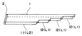
図22は本実施の形態における信号処理装置の構成を示す図である。支持基板20上に、一端に複数の段差を階段状に形成することにより生成された入出射部を有する光信号伝達装置10が複数(本実施の形態では4つ)並置されている。
【0074】
図21は、図20に用いられている板状の光信号伝達装置10を示す。光信号伝達装置10は階段状の複数の光信号入出射部141乃至144を有している。回路基板50の入出射手段からの光信号を送受信する入出射部142乃至144の面は光信号伝達装置10の上面に対して45°の角度をなすように形成され、外部装置と光信号の送受信を行うために光ファイバ181、182の端部と接続される入出射部141の面は光信号伝達装置10の上面に対して垂直に形成されている。
【0075】
図20は、図20で示されている光信号装置の構成を示す断面図である。複数の回路基板50の各々には、複数の発光・受光素子52が備えられており、発光・受光素子52と光信号伝達装置10の複数の入出射部のうち入出射部142、143、144とが対向するように、光信号伝達装置の上部に複数の回路基板50が互いに平行に立設される。
【0076】
光信号伝達装置10の入出射部141には外部装置と光信号の送受信を行うために、各々入力用光ファイバ181、及び出力用光ファイバ182が接続されている。光ファイバ181、182は支持基板20上に固定されたコネクタ184の一方に接続される。コネクタ184の他方には、外部装置の光信号を送受信する光ファイバが接続される。
【0077】
光ファイバ181を介して外部装置から光信号が送信される場合は、入射部141から光信号伝達装置10に光信号が入射される。他の入出射部142乃至144から光信号伝達装置10に光信号が入射された場合には、入出射部141から出射された光信号が光ファイバ182を介して外部装置に送信される。なお、入出射部142乃至144からの光信号の入射及び出射と光信号伝達装置10内における光信号の反射・伝播については第1乃至第5の実施例と同様であるので、詳細を記述しない。
【0078】
本実施の形態では、光信号伝達装置10の入出射部の一部に光ファイバを接続し、外部装置の光信号を送受信する光ファイバとコネクタを介して接続する構成により、信号処理装置と外部装置との光結合を容易に行うことができる。
【0079】
なお、この際、外部装置の有する光ファイバは、該コネクタ184に対し脱着可能であってよい。また、光信号伝達装置10(即ち、入出射部141)に直接コネクタを設けて光信号伝達装置10と外部装置とを接続する光ファイバを接続してもよい(図23)。本実施の形態では、光ファイバは入出射部141に接続されたが、本発明はこれに限定されない。光ファイバは何れの単数又は複数の入出射部に接続されてもよい。
【0080】
図15〜図17は、それぞれ第1実施の形態及び第2実施の形態に示した光信号伝達装置10を複数使った光データバス30の構成について示している。即ち、図15には、第1の実施の形態に係る光信号伝達装置(図1参照)を複数厚さ方向に重ねた構成を示し、図16には、第2の実施の形態に係る光信号伝達装置10(図2参照)を複数幅方向に重ねた構成を示している。図17(A)には、第2の実施の形態に係る光信号伝達装置10(図2参照)を複数厚さ方向に重ねた構成を示し、図17(B)は、図17(A)に示した構成の変形例であり、入出射部の面が透光性媒体1の奥側側面又は手前側側面に対して45°に形成された構成を示している。なお、ここで示した構成は、一例であり、図3に示される光信号伝達装置10を組合せる構成なども可能である。
【0081】
【発明の効果】
以上説明したように本発明は、一端に光信号を入射及び出射するための複数の入出射部を有する透光性媒体と、入出射部から入射された光信号を、複数の入出射部方向に反射する透光性媒体の他端に配置された反射手段と、を有する光信号伝達装置を提供することにより、信号処理装置の構成が容易となり、光信号の利用効率を高くすることができる。
【図面の簡単な説明】
【図1】 第1の実施の形態に係る光信号伝達装置の概略構成図である。
【図2】 第2の実施の形態に係る光信号伝達装置の概略構成図である。
【図3】 第2の実施の形態に係る光信号伝達装置の変形例を示した概略構成図である。
【図4】 第2の実施の形態に係る光信号伝達装置における光信号の入出射状態を示した図である。
【図5】 第2実施形態における出射光効率を示す図である。
【図6】 第2実施形態における出射光強度の均一性を示す図である。
【図7】 L2、L1を示した図である。
【図8】 L2とL1を変化させた場合の光線追跡シミュレーションにおける出射光強度の均一性を示す図である。
【図9】 L2とL1を変化させた場合の光線追跡シミュレーションにおける出射光強度の均一性を示す他の図である。
【図10】 L2とL1を変化させた場合の光線追跡シミュレーションにおける出射光強度の均一性を示す更に他の図である。
【図11】 出射光強度の均一性を可能とする構成の概念説明図である。
【図12】 第3の実施の形態に係る光信号伝達装置の概略構成図である。
【図13】 光データバスを使った信号処理装置を示す斜視図である。
【図14】 光データバスを使った信号処理装置の他の例を示す斜視図である。
【図15】 本発明の第1実施形態の光信号伝達装置を複数使用した光データバスの構成例を示した図である。
【図16】 本発明の第2実施形態の光信号伝達装置を複数使用した光データバスの構成例を示した図である。
【図17】 本発明の第2実施形態の光信号伝達装置を複数使用した光データバスの他の構成例を示した図である。
【図18】 本発明の第4実施形態における回路基板上の発光・受光素子と光信号伝達装置の入出射部との位置関係を示す図である。
【図19】 本発明の第5実施形態における回路基板上の発光・受光素子と光信号伝達装置の入出射部との位置関係を示す図である。
【図20】 本発明の第6実施形態の光信号伝達装置と外部装置を光ファイバで接続する信号処理装置の構成例を示した図である。
【図21】 本発明の第6実施形態の光信号伝達装置を示した図である。
【図22】 本発明の第6実施形態における回路基板上の発光・受光素子と光信号伝達装置の入出射部との位置関係を示す図である。
【図23】 本発明の第6実施形態の変形例である、直接コネクタを光信号伝達装置に設けた場合の拡大図である。
【符号の説明】
1 透光性媒体
2 反射型光拡散層
10 光信号伝達装置
13、14 入出射部
20 支持基板
30 光データバス
40 コネクタ
50 回路基板
51 電子回路
52 発光・受光素子[0001]
BACKGROUND OF THE INVENTION
The present invention relates to an optical signal transmission device, an optical data bus system, and a signal processing device. More specifically, the present invention relates to an optical signal transmission device that emits an incident optical signal in a branched state, and the optical signal transmission device. The present invention relates to an optical data bus system and a signal processing device used.
[0002]
[Prior art]
With the development of very large scale integrated circuits (VLSI), the circuit functions of circuit boards (daughter boards) used in data processing systems have increased significantly. As the circuit function increases, the number of signal connections to each circuit board increases, so a data bus board (motherboard) that connects each circuit board (daughter board) with a bus structure requires a large number of connection connectors and connection lines. A parallel architecture is adopted. Although parallel buses have been improved by increasing the number of connection lines and paralleling them, parallel bus operation speeds have been improved. However, the system processing speed has been increased in parallel due to signal delays due to inter-connection wiring capacitance and connection wiring resistance. It may be limited by the operating speed of the bus. In addition, the problem of electromagnetic interference (EMI) due to the high density of parallel bus connection wiring is also a major limitation to the improvement of the processing speed of the system.
[0003]
In order to solve such problems and to improve the operation speed of the parallel bus, it has been studied to use an in-system optical connection technique called optical interconnection. An overview of optical interconnection technology is described in Uchida, Circuit Implementation Conference 15C01, p.201-202 and H.Tomimuro et al, IEEE Tokyo Section Denshi Tokyo No.33 p.81-86 (1994). Similarly, various forms have been proposed depending on the configuration contents of the system.
[0004]
Of various types of optical interconnection technologies proposed in the past, Japanese Patent Application Laid-Open No. 2-41042 has devised an optical data transmission system using a light emitting / receiving device. In JP-A-2-41042, light emitting / receiving devices are arranged on both front and back surfaces of each circuit board, and light emitting / receiving devices on adjacent circuit boards incorporated in a system frame are spatially coupled with light, A serial optical data bus has been proposed for loop transmission between circuit boards. In this method, an optical signal sent from a certain circuit board is optically / electrically converted by an adjacent circuit board, and is further electrically / optically converted by the circuit board, and then the optical signal is sent to the adjacent circuit board. Each circuit board is sequentially arranged in series and transmitted between all circuit boards incorporated in the system frame while repeating photoelectric conversion and electrical / optical conversion on each circuit board. For this reason, the signal transmission speed depends on the optical / electrical conversion / electrical / optical conversion speed of the light-receiving / light-emitting device arranged on each circuit board, and at the same time, is restricted. In addition, data transmission between each circuit board uses optical coupling with free space by light receiving / light emitting devices arranged on each circuit board, so interference between adjacent optical data transmission paths (Crosstalk) occurs and data transmission failure is expected. It is also expected that a data transmission failure will occur due to scattering of the optical signal due to the environment in the system frame, such as dust.
[0005]
Japanese Patent Application Laid-Open No. 61-196210 devises a method of optically coupling circuit boards through an optical path composed of a diffraction grating and a reflecting element arranged on the plate surface. In this system, since light emitted from one point can be connected to only one fixed point, it is impossible to connect all circuit boards exhaustively like an electric bus.
[0006]
Also, several patents have been devised for data transmission between circuit boards using an optical connecting device having a branch element.
[0007]
Japanese Patent Application Laid-Open No. 58-42333 shows an example of data transmission between circuit boards using a plurality of half mirrors. However, when a plurality of half mirrors are used, the size of the apparatus increases, and each mirror needs to be optically aligned with the light emitting / receiving device. In addition, the transmitted light that has passed through the half mirror has almost half the light intensity with respect to the incident, so if you repeat branching and transmission multiple times, the light intensity becomes weak, and sufficient light intensity at the light receiving device is obtained. There is a problem that signal transmission becomes impossible.
[0008]
Japanese Patent Application Laid-Open No. 4-134415 has devised a system in which an optical signal is incident from a side surface of a lens array in which a plurality of lenses are formed and is emitted from each lens. In this method, the closer the lens is to the incident position of light, the larger the amount of emitted light, so there is a concern about variations in the intensity of the emitted signal due to the positional relationship between the incident position and the emitted position. In addition, since the rate at which light incident from the side faces escapes from the opposite side faces is high, the utilization efficiency of the incident light amount is low.
[0009]
Japanese Patent Application Laid-Open No. 63-1223 discloses an optical bus system using an optical fiber capable of transmitting a substantially uniform optical signal by increasing the branching ratio sequentially from the input end. A method of forming a coupler applicable to such a system is described in IEEE Photonics Technology Letters, vol. 8, No. 12, December (1996). The method for forming a coupler shown here branches by a V-groove formed in an optical fiber. It is considered possible to adjust the output light amount by adjusting the size of the V-groove, but the production is very difficult and the utilization efficiency of the incident light amount is low.
[0010]
A star coupler that equalizes the intensity of the branched optical signal is disclosed in Japanese Patent Laid-Open No. 9-184941. In general, this star coupler bundles and fixes one end of a plurality of optical fibers, a light guide path wide enough to cover the plurality of optical fibers is abutted on one end face, and a light reflecting means is provided on the other end face. I have.
[0011]
When data transmission between circuit boards is performed using such a coupler, the number of fibers connected to the light emitting / receiving elements increases as the number of connection boards increases, which complicates the configuration and increases the size of the apparatus. Occurs.
[0012]
[Problems to be solved by the invention]
In view of the above circumstances, the present invention provides an optical signal transmission device that is easy to configure, an optical data bus system that uses a plurality of the optical signal transmission devices, and a signal that performs signal processing including transmission and reception of data including the optical data bus. An object is to provide a processing apparatus.
[0013]
[Means for Solving the Problems]
To achieve the above object, the present invention provides an optical signal formed by providing a plurality of steps at one end. For incident or exit or for entrance and exit A translucent medium having a plurality of incident / exit parts, and a reflecting means disposed at the other end of the translucent medium and reflecting an optical signal incident from the incident / exit parts in the direction of the plurality of incident / exit parts An optical signal transmission device comprising:
[0014]
That is, an incident / exit part is formed at one end of the translucent medium by providing a plurality of steps. The plurality of incident / exit portions are formed by providing a plurality of steps in a step shape at one end of the translucent medium. The other end of the translucent medium is provided with a reflecting means for reflecting the optical signal incident from the incident / exiting part toward the plural incident / exiting parts.
[0015]
Therefore, when an optical signal is incident from one of the multiple incident / exit portions, the optical signal passes through the translucent medium and reaches the reflecting means. The optical signal that has reached the reflecting means is reflected in the direction of a plurality of incident / exit portions.
[0016]
In the present invention, the side surface of the translucent medium reflects the optical signal other than the optical signal directly incident on the incident / exiting portion out of the optical signal reflected by the reflecting means so as to guide it to the incident / exiting portion.
[0017]
Of the optical signals reflected by the reflecting means, not only the optical signal directly incident on the incident / exiting part but also the optical signal other than the optical signal that is directly incident are reflected so as to be guided to the incident / exiting part. Can be high.
[0018]
Here, the step lengths of the plurality of steps formed at one end of the translucent medium may be equalized. Further, when the step length of each of the plurality of steps is L1, and the length from the other end of the translucent medium to the incident / exit portion located at the closest position to the other end is L2, the translucent medium A plurality of steps may be provided so as to satisfy L2 ≧ L1.
[0019]
Further, the entrance / exit section of the translucent medium reflects the incident optical signal in the direction of the reflecting means and reflects the optical signal reflected from the reflecting means and the side surface in the direction opposite to the incident direction. Also good. In such a case, the surface of the translucent medium serving as the incident / exit section is formed to be 45 ° with respect to the upper surface of the translucent medium. It is desirable to set the surface to be the incident / exit part to be a total reflection surface. Then, at least one of the plurality of incident / exit portions may reflect the optical signal in a direction different from the reflection direction of the other incident / exit portions.
[0020]
Further, the side surface of the translucent medium reflects an optical signal reflected by the reflecting means other than the optical signal directly incident on the incident / exiting part so as to be guided to the entire plurality of incident / exiting parts. May be.
[0021]
For example, when the diffusion angle of the light diffusing means is 2θ and the maximum prospective angle when the incident / exit portion that is closest to the diffusing means is viewed from the light diffusing means is 2θ ′, the translucent medium satisfies tanθ ≧ tan3θ ′. You may comprise so that a relationship may be satisfy | filled. Further, the translucent medium may be configured to satisfy the relation of θ ≦ φ when the diffusion angle of the light diffusing means is 2θ and the numerical aperture of the translucent medium is sinφ.
[0022]
In this way, since the optical signal reflected by the reflecting means is reflected so that the optical signal other than the optical signal directly incident on the incident / exiting part is guided to the entire plurality of incident / exiting parts, the light utilization efficiency is further improved. Can be improved.
[0023]
The reflection means may diffusely reflect an optical signal incident from the incident / exiting portion in the direction of the plural incident / exiting portions, or may reflect the optical signal specularly.
[0024]
In addition, since the translucent medium has the light incident / exit portions formed by providing a plurality of steps at one end, the circuit board can be provided upright on the translucent medium in parallel with each other. It is possible to arrange light receiving and emitting elements provided on the substrate as the light emitting / receiving means so as to face the light incident / exiting portion, thereby facilitating the configuration.
[0025]
Furthermore, it is possible to configure an optical data bus system that transmits data using an optical signal by using the optical signal transmission device of the present invention.
[0026]
At this time, an optical fiber may be connected to a part of the plurality of input / output portions for optical connection with an external device, and the connection portion may be configured as a connector. Or you may provide the connector for connection with an external apparatus in a part of entrance / exit part.
[0027]
In addition, a signal processing device is proposed that includes the optical signal transmission device of the present invention and a circuit board that is disposed opposite to the input / output unit and has input / output means for entering / exiting the optical signal. That is, when an optical signal carrying data is incident on the incident / exit section using the incident / exit means, the optical signal is branched as described above, and is emitted to the outside through the plurality of incident / exit sections. As the incident / exit means, a light emitting element and a light receiving element can be used, but both the light emitting element and the light receiving element may be provided for each of the incident / exit parts, or may be provided individually.
[0028]
DETAILED DESCRIPTION OF THE INVENTION
Embodiments of the present invention will be described below with reference to the drawings.
[0029]
[First Embodiment]
FIG. 1A shows a schematic configuration diagram of an optical
[0030]
Next, with reference to FIG. 1B, a method of branching the input light of the optical
[0031]
A description will be given of a case where the light is incident from the light incident /
[0032]
Here, in the present embodiment, the
[0033]
That is, when the diffused light diffusely reflected by the reflective
[0034]
In particular, in the present embodiment, the optical
[0035]
Thus, by setting tan θ ≧ 3 tan θ ′, the diffused light signal diffused left and right by the reflective
[0036]
Further, when the divergence angle in the diffusion characteristic of the diffuse reflection part is 2θ and the numerical aperture of the translucent medium is sin φ, the relationship θ ≦ φ is satisfied, that is, the upper and lower surfaces of the
[0037]
As described above, according to the optical signal transmission device of the present embodiment, it is possible to improve the utilization efficiency of the incident optical signal and to evenly divide the light, and to make the output level uniform in the emission part. .
[0038]
In the embodiment described above, the optical
[0039]
Further, at the time of input, the collimated laser light does not travel straight through the
[0040]
Further, a clad layer (not shown) having a refractive index smaller than that of the
[0041]
As the reflective
[0042]
[Second Embodiment]
Next, a second embodiment of the present invention will be described. In the present embodiment, since there are the same components as those in the first embodiment described above, the same portions are denoted by the same reference numerals, description thereof will be omitted, and different portions will be described.
[0043]
FIG. 2A shows a schematic configuration of the optical
[0044]
Next, with reference to FIG. 2B, a method of branching the input light of the optical
[0045]
Here, the case where it enters from the incident /
[0046]
The diffused and diffused light propagates while being reflected by the side surface in the
[0047]
The incident / exit direction is not limited to the vertical direction (upper surface direction), and may be the vertical direction (lower surface direction) and the width direction (left / right direction). The incident / exit direction can be changed depending on the surface formation direction of the incident / exit portion. is there. For example, as shown in FIGS. 3A to 3D, various incident / exit directions can be combined.
[0048]
3 (A) and 3 (B) show the
[0049]
3 (C) and 3 (D) show the
[0050]
5 and 6, as shown in FIGS. 4A to 4D, in the second embodiment, the total length H1 of the
[0051]
As shown in FIG. 5, the efficiency of the outgoing light at each incoming / outgoing part is approximately 18% regardless of which incoming / outgoing part is incident (
[0052]
As the light source, an edge-emitting laser diode that emits light having a wavelength of 680 nm is used.
[0053]
8 to 10 show a distance 11 from the end face where the reflective
[0054]
[Third Embodiment]
Next, a third embodiment of the present invention will be described. Since the present embodiment is the same as the first and second embodiments described above, the same parts are denoted by the same reference numerals and the description thereof is omitted.
[0055]
FIG. 12A shows a schematic configuration of the optical
[0056]
In FIG. 12B, each surface of the incident /
[0057]
Next, a method for branching input light of the optical
[0058]
The reflected laser light is propagated while being reflected by the side surface in the
[0059]
For this reason, when the light reflected by the
[0060]
As described above, in the present embodiment described above, the optical
[0061]
Furthermore, a clad layer (not shown) having a refractive index smaller than that of the
[0062]
According to the present embodiment, by using a material capable of specular reflection such as Al for the
[0063]
[Fourth Embodiment]
Next, a fourth embodiment of the present invention will be described. As shown in FIG. 13, the signal processing apparatus according to the present embodiment has a plurality of
[0064]
That is, in the signal processing device according to the present embodiment, the
[0065]
A
[0066]
Each
[0067]
[Fifth Embodiment]
Next, a fifth embodiment of the present invention will be described. As shown in FIG. 14, a plurality of signal processing apparatuses according to this embodiment are provided by an
[0068]
In the signal processing apparatus (FIG. 13) according to the fourth embodiment, the plurality of
[0069]
That is, as shown in FIG. 19, the incident /
[0070]
With this arrangement, each light emitting / receiving
[0071]
As described above, in the fourth embodiment and the fifth embodiment, a signal processing device having a plurality of circuit boards is configured using an optical data bus including the present optical signal transmission device. Signal transmission between the circuit boards is possible, and since a translucent material is used as a transmission medium, an optical bus system having high resistance to temperature changes and environmental changes such as dust can be obtained.
[0072]
[Sixth Embodiment]
In the first to fifth embodiments, the light emitting / receiving elements provided on the circuit board as the optical signal input / output means for transmitting / receiving the optical signal to / from the optical signal transmission device are shown. Here, an embodiment will be described in which the optical signal transmission device transmits and receives an optical signal to and from an external device other than a circuit board, such as an image scanner.
[0073]
FIG. 22 is a diagram illustrating a configuration of the signal processing device according to the present embodiment. On the
[0074]
FIG. 21 shows the plate-like optical
[0075]
20 is a cross-sectional view showing the configuration of the optical signal device shown in FIG. Each of the plurality of
[0076]
An input
[0077]
When an optical signal is transmitted from an external device via the
[0078]
In the present embodiment, an optical fiber is connected to a part of the incident / exit section of the optical
[0079]
At this time, the optical fiber of the external device may be detachable from the
[0080]
FIGS. 15 to 17 show the configuration of an
[0081]
【The invention's effect】
As described above, the present invention provides a translucent medium having a plurality of input / output portions for entering and exiting an optical signal at one end, and an optical signal incident from the input / output portions in a plurality of input / output portion directions. By providing an optical signal transmission device having reflection means disposed at the other end of the translucent medium that reflects light, the configuration of the signal processing device becomes easy and the utilization efficiency of the optical signal can be increased. .
[Brief description of the drawings]
FIG. 1 is a schematic configuration diagram of an optical signal transmission device according to a first embodiment.
FIG. 2 is a schematic configuration diagram of an optical signal transmission device according to a second embodiment.
FIG. 3 is a schematic configuration diagram showing a modification of the optical signal transmission device according to the second embodiment.
FIG. 4 is a diagram showing an incident / exit state of an optical signal in an optical signal transmission device according to a second embodiment.
FIG. 5 is a diagram showing the emitted light efficiency in the second embodiment.
FIG. 6 is a diagram showing uniformity of emitted light intensity in the second embodiment.
FIG. 7 is a diagram showing L2 and L1.
FIG. 8 is a diagram showing the uniformity of emitted light intensity in a ray tracing simulation when L2 and L1 are changed.
FIG. 9 is another diagram showing the uniformity of the emitted light intensity in the ray tracing simulation when L2 and L1 are changed.
FIG. 10 is still another diagram showing the uniformity of the emitted light intensity in the ray tracing simulation when L2 and L1 are changed.
FIG. 11 is a conceptual explanatory diagram of a configuration that enables uniformity of emitted light intensity.
FIG. 12 is a schematic configuration diagram of an optical signal transmission device according to a third embodiment.
FIG. 13 is a perspective view showing a signal processing device using an optical data bus.
FIG. 14 is a perspective view showing another example of a signal processing device using an optical data bus.
FIG. 15 is a diagram showing a configuration example of an optical data bus using a plurality of optical signal transmission devices according to the first embodiment of the present invention.
FIG. 16 is a diagram showing a configuration example of an optical data bus using a plurality of optical signal transmission devices according to the second embodiment of the present invention.
FIG. 17 is a diagram showing another configuration example of an optical data bus using a plurality of optical signal transmission devices according to the second embodiment of the present invention.
FIG. 18 is a diagram showing a positional relationship between a light emitting / receiving element on a circuit board and an incident / exit portion of an optical signal transmission device in a fourth embodiment of the present invention.
FIG. 19 is a diagram showing a positional relationship between light emitting / receiving elements on a circuit board and an input / output part of an optical signal transmission device according to a fifth embodiment of the present invention.
FIG. 20 is a diagram illustrating a configuration example of a signal processing device that connects an optical signal transmission device according to a sixth embodiment of the present invention and an external device through an optical fiber.
FIG. 21 is a diagram showing an optical signal transmission device according to a sixth embodiment of the present invention.
FIG. 22 is a diagram showing a positional relationship between a light emitting / receiving element on a circuit board and an incident / exit portion of an optical signal transmission device in a sixth embodiment of the present invention.
FIG. 23 is an enlarged view showing a modification of the sixth embodiment of the present invention when a direct connector is provided in the optical signal transmission device.
[Explanation of symbols]
1 Translucent medium
2 Reflective light diffusion layer
10 Optical signal transmission device
13, 14 Input / output part
20 Support substrate
30 Optical data bus
40 connectors
50 circuit board
51 Electronic circuit
52 Light emitting / receiving element
Claims (15)
前記透光性媒体の他端に配置され、前記入出射部から入射された光信号を、前記複数の入出射部方向に反射する反射手段と、
を備えた光信号伝達装置。A translucent medium formed by providing a plurality of steps at one end, and having a plurality of incident and exit portions for entering or emitting an optical signal or entering and emitting;
Reflecting means disposed at the other end of the translucent medium and reflecting an optical signal incident from the incident / exiting portion toward the plurality of incident / exiting portions;
An optical signal transmission device comprising:
を備える光データバスシステム。An optical data bus system comprising:
前記入出射部に対向するように配置された光信号を入出射する入出射手段を有する回路基板と、A circuit board having input / output means for entering / exiting an optical signal arranged so as to face the input / output part;
を備えた信号処理装置。A signal processing apparatus comprising:
Priority Applications (2)
| Application Number | Priority Date | Filing Date | Title |
|---|---|---|---|
| JP2000252661A JP3752981B2 (en) | 1999-09-08 | 2000-08-23 | Optical signal transmission device, optical data bus system, and signal processing device |
| US09/655,426 US6792213B1 (en) | 1999-09-08 | 2000-09-05 | Optical signal transmitting apparatus, optical data bus system and signal processing apparatus |
Applications Claiming Priority (5)
| Application Number | Priority Date | Filing Date | Title |
|---|---|---|---|
| JP25405799 | 1999-09-08 | ||
| JP2000168955 | 2000-06-06 | ||
| JP2000-168955 | 2000-06-06 | ||
| JP11-254057 | 2000-06-06 | ||
| JP2000252661A JP3752981B2 (en) | 1999-09-08 | 2000-08-23 | Optical signal transmission device, optical data bus system, and signal processing device |
Publications (3)
| Publication Number | Publication Date |
|---|---|
| JP2002062457A JP2002062457A (en) | 2002-02-28 |
| JP2002062457A5 JP2002062457A5 (en) | 2005-05-19 |
| JP3752981B2 true JP3752981B2 (en) | 2006-03-08 |
Family
ID=27334288
Family Applications (1)
| Application Number | Title | Priority Date | Filing Date |
|---|---|---|---|
| JP2000252661A Expired - Fee Related JP3752981B2 (en) | 1999-09-08 | 2000-08-23 | Optical signal transmission device, optical data bus system, and signal processing device |
Country Status (1)
| Country | Link |
|---|---|
| JP (1) | JP3752981B2 (en) |
Families Citing this family (5)
| Publication number | Priority date | Publication date | Assignee | Title |
|---|---|---|---|---|
| JP2002131591A (en) * | 2000-10-27 | 2002-05-09 | Fuji Xerox Co Ltd | Optical signal transmitting device and light incident method into translucent medium |
| JP4039192B2 (en) | 2002-09-20 | 2008-01-30 | 富士ゼロックス株式会社 | Optical transmission equipment |
| JP2007133036A (en) * | 2005-11-08 | 2007-05-31 | Mitsui Chemicals Inc | Optical multiplexing/demultiplexing element |
| US7925168B2 (en) * | 2007-10-16 | 2011-04-12 | Hewlett-Packard Development Company, L.P. | Optical interconnect system providing communication between computer system components |
| US9261643B2 (en) | 2009-07-20 | 2016-02-16 | 3M Innovative Properties Company | Hollow lightguide having multiple reflectors |
-
2000
- 2000-08-23 JP JP2000252661A patent/JP3752981B2/en not_active Expired - Fee Related
Also Published As
| Publication number | Publication date |
|---|---|
| JP2002062457A (en) | 2002-02-28 |
Similar Documents
| Publication | Publication Date | Title |
|---|---|---|
| US6792213B1 (en) | Optical signal transmitting apparatus, optical data bus system and signal processing apparatus | |
| JP3862794B2 (en) | Optical bus and signal processing device | |
| JP3666190B2 (en) | Optical bus and signal processing device | |
| JP3752981B2 (en) | Optical signal transmission device, optical data bus system, and signal processing device | |
| US5987198A (en) | Optical bus and optical bus production method including a plurality of light transmission paths | |
| JP3837980B2 (en) | Optical branching device and optical bus circuit using the same | |
| JP3988357B2 (en) | Optical bus circuit board | |
| JP3785919B2 (en) | Optical signal transmission device, optical data bus system, and signal processing device | |
| JP3815186B2 (en) | Signal processing circuit and optical bus device | |
| JP3752967B2 (en) | Optical branching device | |
| JP3925081B2 (en) | Optical coupling device | |
| JP3896720B2 (en) | Optical data bus and signal processing apparatus | |
| JP2002040302A (en) | Optical bus circuit system | |
| JP3752977B2 (en) | Optical data bus and opto-electric hybrid board | |
| JP3932747B2 (en) | Optical branching device and optical network | |
| JP2002131591A (en) | Optical signal transmitting device and light incident method into translucent medium | |
| JP3820881B2 (en) | Optical signal transmission device | |
| JP3744278B2 (en) | Signal processing device | |
| JP2002243973A (en) | Optical bus circuit board | |
| JP3610689B2 (en) | Optical bus and signal processing device | |
| JP3635878B2 (en) | Optical data bus, optical data bus complex, and signal processing apparatus | |
| JP2003322769A (en) | Optical transmission module | |
| JP2004226611A (en) | Optical demultiplexing and multiplexing device | |
| JP2001075690A5 (en) | ||
| JP2002258097A (en) | Optical signal transmitting device, translucent medium, and optical data bus system |
Legal Events
| Date | Code | Title | Description |
|---|---|---|---|
| A521 | Written amendment |
Free format text: JAPANESE INTERMEDIATE CODE: A523 Effective date: 20040715 |
|
| A621 | Written request for application examination |
Free format text: JAPANESE INTERMEDIATE CODE: A621 Effective date: 20040715 |
|
| A977 | Report on retrieval |
Free format text: JAPANESE INTERMEDIATE CODE: A971007 Effective date: 20051115 |
|
| TRDD | Decision of grant or rejection written | ||
| A01 | Written decision to grant a patent or to grant a registration (utility model) |
Free format text: JAPANESE INTERMEDIATE CODE: A01 Effective date: 20051122 |
|
| A61 | First payment of annual fees (during grant procedure) |
Free format text: JAPANESE INTERMEDIATE CODE: A61 Effective date: 20051205 |
|
| R150 | Certificate of patent or registration of utility model |
Free format text: JAPANESE INTERMEDIATE CODE: R150 |
|
| FPAY | Renewal fee payment (event date is renewal date of database) |
Free format text: PAYMENT UNTIL: 20091222 Year of fee payment: 4 |
|
| FPAY | Renewal fee payment (event date is renewal date of database) |
Free format text: PAYMENT UNTIL: 20101222 Year of fee payment: 5 |
|
| FPAY | Renewal fee payment (event date is renewal date of database) |
Free format text: PAYMENT UNTIL: 20111222 Year of fee payment: 6 |
|
| FPAY | Renewal fee payment (event date is renewal date of database) |
Free format text: PAYMENT UNTIL: 20111222 Year of fee payment: 6 |
|
| FPAY | Renewal fee payment (event date is renewal date of database) |
Free format text: PAYMENT UNTIL: 20121222 Year of fee payment: 7 |
|
| FPAY | Renewal fee payment (event date is renewal date of database) |
Free format text: PAYMENT UNTIL: 20121222 Year of fee payment: 7 |
|
| FPAY | Renewal fee payment (event date is renewal date of database) |
Free format text: PAYMENT UNTIL: 20131222 Year of fee payment: 8 |
|
| LAPS | Cancellation because of no payment of annual fees |