JP3738342B2 - Communication terminal device and storage medium - Google Patents
Communication terminal device and storage medium Download PDFInfo
- Publication number
- JP3738342B2 JP3738342B2 JP16859499A JP16859499A JP3738342B2 JP 3738342 B2 JP3738342 B2 JP 3738342B2 JP 16859499 A JP16859499 A JP 16859499A JP 16859499 A JP16859499 A JP 16859499A JP 3738342 B2 JP3738342 B2 JP 3738342B2
- Authority
- JP
- Japan
- Prior art keywords
- transmission
- cpu
- data
- received
- communication
- Prior art date
- Legal status (The legal status is an assumption and is not a legal conclusion. Google has not performed a legal analysis and makes no representation as to the accuracy of the status listed.)
- Expired - Fee Related
Links
Images


Landscapes
- Optical Communication System (AREA)
Description
【0001】
【発明の属する技術分野】
本発明は、光通信を行うことができる通信端末装置に関する。
【0002】
【従来の技術】
近年、パソコンや情報携帯端末(例えば、ハンディターミナル等)におけるデータ通信インタフェースとして、赤外光を用いて赤外線データ通信機能が搭載されるようになってきている。このような機器には、赤外線データ通信に対応して、受発光素子及びその駆動回路などから成る通信素子が、その受発光面を形成する側面などに取付けられている。送信側の発光素子には発光ダイオード等が、受信側の受光素子にはフォトトランジスタ等が用いられている。
【0003】
現在、上述のような赤外線データ通信に用いられている通信方式として、IrDA(Infrared Data Association:赤外線データ通信協議会)で採択された代表的な標準化方式としての標準プロトコルとしてIrDAが用意されている。
【0004】
ここで、IrDA通信においては、AGC(Automatic Gain Control)によって受信した光信号のパルス値を成形するスレッシュレベルを決定していた。
【0005】
【発明が解決しようとする課題】
しかしながら、受信した光信号のパルス波形を基にスレッシュレベルを決定している従来のIrDA通信方式においては、光信号の通信速度若しくは受光量の変化又は外光等によるノイズの影響が問題となっていた。
【0006】
つまり、通信速度が速くしかも大きい光エネルギーの光信号を受信するときには、AGCの受信利得補正によりスレッシュレベルを適正なレベルに安定させて波形成形が可能であり、ノイズの影響を軽減して安定した通信となるが、通信信号の光エネルギーが同じであっても通信速度が遅く、その通信速度よりノイズの発生周期が早い場合には、AGCにより設定されるスレッシュレベルが低くなってしまい、その結果ノイズ成分もパルス波形として成形されるため、正確なデータ通信が不可能になるという問題があった。
【0007】
また、従来のIrDA通信においては、機器間の通信距離の変化又は外光の侵入による外乱等の影響により、受光素子に対する受光量が変化するので、受光素子の受光感度の調整が非常に困難であるという問題もあった。
【0008】
更に、同一構成の情報通信端末間でIrDA通信を行う場合は、各情報通信端末の受発光部を互いに向き合わせて行わなければならず、オペレータが一人で通信するときにどちらか一方は、その表示部の表示内容が上下逆さまとなり、通信中の表示内容の確認が困難になる場合があるという問題もあった。
【0009】
本発明の課題は、光信号の通信速度や受光量の変化に応じてスレッシュレベルと受光感度を適宜制御するとともに、通信中の表示内容の確認を容易にする表示制御を行う通信端末装置を提供することである。
【0010】
【課題を解決するための手段】
請求項1に記載の通信端末装置は、光通信によってデータを送受信するための発光部と受光部とを備えた通信端末装置において、一方の通信端末装置は、受信時に前記受光部で受光された受光光度に基づいて基準値との差より補正値を求める手段と、前記求められた補正値を他方の通信端末装置へ送信する手段と、前記補正値を受信した他方の通信端末装置は、受信した前記補正値に基づいて前記発光部の発光光度を制御する手段と前記制御された発光光度によりデータを送信する発光部とを備える。
【0019】
【発明の実施の形態】
以下、図を参照して本発明の実施の形態を詳細に説明する。
図1から図14までの図は、本発明を適用したハンディターミナルの一実施の形態を示す図である。
まず、構成を説明する。
【0020】
本実施の形態におけるハンディターミナル(請求項1〜5において、通信端末装置)1は、その制御系の要部構成は、図1に示すブロック図のように、CPU(請求項3記載の検出手段及び発光光度調整手段に、並びに請求項4記載の判別手段及び表示制御手段に対応する。)11、入力装置12、表示装置13、RAM14、撮像部15、送信部(請求項1及び請求項3記載の送信制御手段に対応する。)16、受信部(請求項1記載の受信制御手段に対応する。)17、記憶装置18、及び記憶媒体19により構成されており、記憶媒体19を除く各部はバス20に接続されている。
【0021】
CPU(Central Processing Unit)11は、記憶装置18内に格納されているシステムプログラム及び当該システムに対応する各種アプリケーションプログラムの中から指定されたアプリケーションプログラムをRAM14内の図示しないプログラム格納領域に展開し、入力装置12から入力される各種指示あるいはデータをRAM14内に一時的に格納し、この入力指示及び入力データに応じて記憶装置18内に格納されたアプリケーションプログラムに従って各種処理を実行し、その処理結果をRAM14内に格納するとともに、表示装置13に表示する。そして、入力装置12による入力指示に従って、RAM14に格納した処理結果を記憶装置18内の所定の保存先に保存する。
【0022】
また、CPU11は、指定された特定のハンディターミナルとの間で光通信処理を実行する際には、記憶装置18内に格納されたOS(Operating System)プログラムにより指定されたIrDA通信プロトコル等に基づいて、後述する光通信処理(図6参照)を実行し、特定のハンディターミナルとの間の光通信結果を表示装置13に表示する。
【0023】
入力装置12は、カーソルキー、数字入力キー及び各種機能キー等を備えたキーボードを含み、押下されたキーの押下信号をCPU11に出力する。
【0024】
表示装置13は、液晶表示パネルにより構成され、CPU11から入力される表示データを表示する。
【0025】
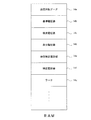
RAM(Random Access Memory)14は、図2に示すように、送信するためのデータを格納する送信対象データメモリ14aと、特定された基準電圧値を格納する基準電圧値メモリ14bと、検出された電圧値を格納する検出電圧値メモリ14cと、基準電圧値と検出電圧値の差分の電圧値を格納する差分電圧値メモリ14dと、補正電圧値の1単位当たりの電圧値を格納する単位補正電圧値メモリ14eと、可変抵抗により得られた補正電圧値を格納する補正電圧値メモリ14fと、上記CPU11により実行される撮像処理、送受信処理、表示モード選択処理、あるいは電圧値補正処理に際して必要な各種プログラムや各種データ等を一時的に展開するワークメモリ14gと、から構成される。
【0026】
撮像部15は、CCDカメラよりなり、CPU11が後述する撮像処理又は表示モード選択処理を実行する際に、オペレータを撮像し、その撮像データをCPU11に出力する。
【0027】
送信部16は、光通信用の送信機能を有し、図3に示す回路構成図のように、抵抗R1、R2、可変抵抗VR、トランジスタTR1、TR2、発光ダイオードD1、インバータINV、及びオアゲートORから構成され、入力端子T1〜T4を備えている。なお、抵抗R1の抵抗値r1と可変抵抗VRの設定抵抗値rとの大小関係は、r1>rである。
【0028】
図3において、入力端子T1にはCPU11から発光ダイオードD1を駆動する発光駆動信号LEDAが入力され、入力端子T2にはCPU11から可変抵抗VRの抵抗値rを補正する補正信号が入力され、入力端子T3にはCPU11から送信モード信号TXmodeが入力され、入力端子T4にはCPU11から送信データTXDが入力される。
【0029】
送信部16は、CPU11により実行される光通信処理に際して入力端子T1〜T4に入力される上記各信号により制御され、送信時は、入力端子T3に入力される送信モード信号TXmodeが“Hi”になり、トランジスタTR1をONさせて、入力端子T1に入力される発光駆動信号LEDAを可変抵抗VRを介して発光ダイオードD1に入力させて、その発光駆動信号LEDAにより発光ダイオードD1を発光させる。
【0030】
また、この時、入力端子T3に入力される送信モード信号TXmodeがインバータINVにより、その出力が“Lo”となり、入力端子T4に入力される送信データTXDをオアゲートORと抵抗R2を介してトランジスタTR2のベース電極に入力させて、送信データTXDに含まれるパルスデータ(“Hi”と“Lo”)のタイミングでトランジスタTR2をON/OFFさせて、発光ダイオードD1を送信データTXDに応じて発光させる。
【0031】
また、送信部16は、受信時は、入力端子T3に入力される送信モード信号TXmodeが“Lo”になって、トランジスタTR1をOFFさせて、インバータINVの出力が“Hi”となって、トランジスタTR2をONさせて、入力端子T1に入力される発光駆動信号LEDAを抵抗R1を介して発光ダイオードD1に入力させて、その発光駆動信号LEDAにより発光ダイオードD1を微弱発光させる。
【0032】
また、送信部16内の可変抵抗VRの設定抵抗値rは、CPU11により実行される光通信処理に際して、送信先のハンディターミナルからの受信応答状態に応じて発光ダイオードD1の発光光度を調整するため、CPU11から入力される補正信号により適宜調整される。
【0033】
なお、送信部16は、図4に示すような回路構成としてもよく、この場合には、送信時は、送信データTXDに含まれるパルスデータ(“Hi”と“Lo”)のタイミングでトランジスタTR1とTR2が同期をとるようにON/OFFさせて、発光ダイオードD1を送信データTXDに応じて発光させる。
【0034】
ここで、入力端子T5には、発光制御信号が入力され、送信時には“Lo”に、受信時には“Hi”になるため、送信部16は、受信時には、入力端子T4に入力される送信データTXDが“Lo”になり、トランジスタTR1をOFFさせて、入力端子T5に入力される発光制御信号が“Hi”となって、トランジスタTR2をONさせて、入力端子T1に入力される発光駆動信号LEDAを抵抗R1を介して発光ダイオードD1に入力させて、その発光駆動信号LEDAにより発光ダイオードD1を微弱発光させる。
【0035】
また、設定された通信速度が外光によるノイズ信号の発生周期より速い場合には、後述するコンパレータがAGC信号に応じて設定するスレッシュレベルは下がらず、ノイズ信号の影響を受けにくい。このため、外光によるノイズ信号の発生周期よりも設定された通信速度が速い場合には、受信時においても発光制御信号を“Lo”とすることにより、通信速度に応じて微弱発光することなく受信することができる。
【0036】
受信部17は、光通信用の受信機能を有し、図5に示す構成図のように、フォトトランジスタ171、アンプ(Amp)172、フィルタ173、自動利得制御部(AGC)174、コンパレータ175、及びA/Dコンバータ176から構成されている。
【0037】
図5において、受信部17は、図3に示したような送信部16により送信データTXDに応じて発光された発光信号をフォトトランジスタ171で受光する。フォトトランジスタ171は、その受光光量の変化に応じて光電変換した受光信号をアンプ172に出力する。アンプ172は、フォトトランジスタ171から入力された受光信号を所定の増幅率で増幅し、その増幅した受光信号をフィルタ173とA/Dコンバータ176に出力する。
【0038】
フィルタ173は、アンプ172から入力された受光信号に含まれた高域雑音成分等を除去して自動利得制御部174に出力し、自動利得制御部174は、フィルタ173から入力された受光信号の波高値レベル等を一定にしてコンパレータ175に出力する。
【0039】
コンパレータ175は、自動利得制御部174から入力された受光信号の電圧値と予め設定された基準電圧値とを比較し、その比較結果として“Hi”レベルと“Lo”レベルを交互に変化する受信データRXDをCPU11に出力する。A/Dコンバータ176は、アンプ172から入力された受光信号を所定のサンプリングタイミングでサンプリングし、そのサンプリングした受光信号の電圧値を所定のビット数でA/D変換して、検出電圧値を示すデジタルデータをCPU11に出力する。
【0040】
図1の記憶装置18は、プログラムやデータ等が予め記憶されている記憶媒体19を有しており、この記憶媒体19は磁気的、光学的記録媒体、若しくは半導体メモリで構成されている。この記憶媒体19は記憶装置18に固定的に設けたもの、若しくは着脱自在に装着するものであり、この記憶媒体19には上記システムプログラム、各種アプリケーションプログラム、及び各処理プログラムで処理されたデータ等を記憶する。
【0041】
また、この記憶媒体19に記憶するプログラム、データ等は、通信回線等を介して接続された他の機器から受信して記憶する構成にしてもよく、更に、通信回線等を介して接続された他の機器側に上記記憶媒体を備えた記憶装置を設け、この記憶媒体19に記憶されているプログラム、データを通信回線等を介して使用する構成にしてもよい。
【0042】
次に、本実施の形態の動作を図6〜図9及び図14のフローチャート並びに図10〜図13により説明する。
【0043】
図6は、ハンディターミナルにより実行される入力処理及び通信処理(送信処理、受信処理)を説明するためのフローチャートである。このフローチャートに記載した各機能を実現するプログラム等はそれぞれハンディターミナルのCPU11が読み取り可能なプログラムコードの形態で上記記憶媒体19に記憶されている。
【0044】
CPU11は、ハンディターミナルの電源がONされているときは常時、オペレータから何らかのキー入力の有無を確認しながら待機している(ステップS1)。また、キー入力がない場合は、オペレータによるIrDA通信の選択の有無を確認する(ステップS5)。
【0045】
オペレータによるキー入力があると、CPU11は、その入力が通常のキー入力か撮像指示入力かを判断する(ステップS2)。通常のキー入力の場合には、CPU11は、そのキー入力に対応した処理を実行し(ステップS3)、キー入力内容を表示装置13に表示する。
【0046】
また、撮像指示入力の場合には、CPU11は、撮像部15によりオペレータを撮像処理して(ステップS4)、撮像データを記憶媒体19に保存する。
【0047】
オペレータによるIrDA通信が選択されると、CPU11は、その選択された通信が送信処理か受信処理かを判断する(ステップS6)。
【0048】
送信処理が選択された場合には、ステップS8に進み、CPU11は、図7に示す送信処理のフローチャートにより送信処理を実行する。また、送信処理が選択されていない場合には、ステップS7に進み、CPU11は、他のハンディターミナルから当該ハンディターミナルへの送信の要求であるかを判断する。
【0049】
他のハンディターミナルからの送信要求であるときは、ステップS9に進み、CPU11は、図8に示す受信処理のフローチャートにより受信処理を実行する。
【0050】
次に、送信処理及び受信処理の手順を図7及び図8のフローチャートにより説明する。
【0051】
図7は、ハンディターミナルの送信処理のフローチャートである。図6のフローチャートにおいてステップS8に進むと、CPU11は、図7のフローチャートの送信処理を実行する。
【0052】
送信処理を選択すると、CPU11は、送信処理を開始して、まず、図9のフローチャートに示す表示モード選択処理を行った後(ステップS801)、送信データを選択する(ステップS802)。
【0053】
送信先のハンディターミナルが受信可能状態にあるか否かを確認するために、CPU11は、送信要求を行うと共に(ステップS803)、送信側の通信速度の設定情報を送信先のハンディターミナルに送信する(ステップS804)。
【0054】
次いで、ステップS805では、CPU11は、送信先のハンディターミナルから受信可能な状態であることを示す応答データを受信したか否かを判断する。
【0055】
送信先のハンディターミナルが受信可能であれば、CPU11は、nブロックに分けて送信する送信対象データのうち、1番目の送信対象データを指定し(ステップS806)、その指定した1番目の送信対象データを送信先のハンディターミナルに送信して(ステップS807)、送信対象データを表示装置12に表示して待機し(ステップS808)、この送信に対する送信先ハンディターミナルからの受信応答内容が正常受信か否かを判断する(ステップS809)。
【0056】
CPU11は、送信先のハンディターミナルから異常受信であった旨の応答データを受信すると、ステップS807に戻り再度同一の通信対象データを送信する。また、補正電圧値とともに正常受信であった旨の応答データを受信すると、その補正電圧値に応じて、送信部16内の可変抵抗VRの抵抗値rを制御して、送信部16内の発光ダイオードD1の発光光度を補正する(ステップS810)。
【0057】
ステップS811では、CPU11は、送信対象データの送信が全て終了したか否かを判断する。まだ、送信対象データが残っている場合は、nに「1」を加算して(ステップS812)、ステップS807に戻り、2番目以後のブロックの送信対象データについて同様の送信処理を繰り返す。
【0058】
そして、CPU11は、送信対象データを全て送信したことを確認すると、通信終了の通知を送信先のハンディターミナルに送信して送信処理を終了する(ステップS813)。
【0059】
これにより、nブロックに分けて送信する送信対象データについて、各ブロック毎に送信部16内の発光ダイオードD1の発光光度を補正することができ、送信先のハンディターミナルの受信処理が安定すると共に、送信中に発光光度を調整できるため、電力の消費を抑えることができる。
【0060】
図8は、ハンディターミナルの受信処理のフローチャートである。図6のフローチャートにおいてステップS9に進むと、CPU11は、図8のフローチャートの受信処理を実行する。
【0061】
受信処理においても送信処理と同様に、受信処理が選択されると、CPU11は、受信処理を開始して、まず、図9のフローチャートに示す表示モード選択処理を実行した後(ステップS901)、送信側のハンディターミナルから送信要求を正常に受信したか否かを判断する(ステップS902)。
【0062】
送信要求を正常に受信したときは、CPU11は、送信側のハンディターミナルから送信された通信速度の設定情報に応じて発光制御信号をセットして(ステップS903)、受信をする準備ができたことを示す応答データを送信側のハンディターミナルに送信する(ステップS904)。
【0063】
ここまででデータ送受信前の処理を終えると、ステップS905では、CPU11は、受信部17によるデータ受信の有無を判断する。
【0064】
そして、受信部17によりデータが受信されると、ステップS906では、CPU11は、正常に受信ができたか否かを判断する。正常に受信ができた場合、CPU11は、そのデータとして受信された受光光度に基づいて、図14に示す電圧値補正処理のフローチャートによる電圧値補正処理を実行する(ステップS907)。次いで、CPU11は、正常にデータ受信ができたことを示す所定の応答データとともに電圧値補正処理によって得られた補正電圧値を送信部16により送信側のハンディターミナルに通知する(ステップS908)。次いで、CPU11は、受信したデータを記憶媒体19に記憶し、表示装置13に表示する(ステップS910)。
【0065】
また、送信されたデータを正常に受信できなかった場合、CPU11は、当該データの再送信を要求する再送要求データを送信側のハンディターミナルに通知して(ステップS909)、ステップS905に戻り、データを受信できるように待機した状態に戻る。
【0066】
次いで、ステップS911では、CPU11は、送信側のハンディターミナルからの終了通知を受信したか否かを判断する。この終了通知がない場合には、更に次の送信対象データが送信されるので、ステップS905に戻り、データを受信できるように待機した状態に戻る。
【0067】
終了通知を受信した場合、CPU11は、微弱発光させていた発光制御信号のセットがあれば解除して(ステップS912)、受信処理を終了する。
【0068】
図9は、本発明の実施の形態におけるハンディターミナルの送信時及び受信時における表示モード選択処理のフローチャートを示した図である。
【0069】
従来のハンディターミナル相互間で送受信する場合には、図10に示したように、受信側のハンディターミナル32の表示装置13は、送信処理を行っているオペレータから見て反転したものとなっていた。このため、送信処理を行っているオペレータは、受信側のハンディターミナル32に正確に送信データが送信できたか否かを一目で認識することができなかった。
【0070】
本発明の実施の形態におけるハンディターミナルにおいては、CPU11は、表示モード選択処理を開始すると、撮像部15として図11及び図12に示すCCDカメラにおける撮像処理によってオペレータの自動認識を開始する(ステップS11)。
【0071】
ステップS12では、CPU11は、図6に示したフローチャートのステップS4において撮像処理した後に記憶媒体19に記憶されているオペレータの画像情報と一致するか否かを判断する。尚、オペレータの画像は人物イメージが何パターンか予め記憶されており、その何れかと一致するかを判断することとする。
【0072】
オペレータの画像情報と一致した場合、CPU11は、受信側のハンディターミナル22の表示装置13における表示画像を180度反転するモードに設定する(ステップS13)。この状態を図11に示す。
【0073】
図11において、受信側のハンディターミナル22の表示装置13の表示は180度反転しているのに対し、送信側のハンディターミナルの表示装置13の表示はそのままとなっている。
【0074】
これにより、送信側のオペレータは、送信データが受信側のハンディターミナル22に正常に送信できたかが一目で認識でき、ハンディターミナルの送受信時の利便性を向上することができる。
【0075】
また、CCDカメラに取り込まれた情報が記憶媒体19に記憶されていないオペレータの画像情報である場合、受信側のハンディターミナル22のCPU11は、表示装置13の表示をそのままのモードに設定する(ステップS14)。この状態を図12に示す。
【0076】
図12において、受信側のハンディターミナル22における表示装置13の表示及び送信側のハンディターミナル21における表示装置13の表示はそのままとなっている。
【0077】
図13は、ハンディターミナルがIrDA通信により受信したアナログデータ(a)とデジタルデータ(b)の一例を示した図である。
【0078】
図13(a)において、IrDA通信により受信部17が受信信号の受信を開始すると、自動利得制御部174が受信信号の受信レベルを調整して図中のAGC信号としてコンパレータ175に出力し、コンパレータ175がAGC信号に応じて図中のスレッシュレベルを設定して、受信信号に含まれたパルス幅に応じた同図(b)のデジタル値を受信データRXDとして出力する。
【0079】
この受信信号の受信時は、送信部16の発光ダイオードD1は微弱発光しており、この微弱発光が受信部17の受信信号の受光に影響して、図13(a)の受信信号の“Lo”レベルを嵩上げさせる。その結果、受信信号以外に外部から侵入する光の影響、すなわち、図中の受信信号の“Lo”レベル以下に示すような外光によるノイズ信号の影響をマスキングして、コンパレータ175におけるスレッシュレベルに基づく受信信号の“Hi”レベルと“Lo”レベルの比較動作を確実にして、受信信号に含まれたパルス成分を確実に抽出することができる。
【0080】
したがって、設定された通信速度が外光によるノイズ信号の発生周期より長い場合であっても、その受信信号に含まれたパルス成分を適切なデジタルパルス信号に成形することができる。
【0081】
図14は、図8に示す受信処理における電圧値補正処理を示したフローチャートである。
【0082】
本発明の実施の形態におけるハンディターミナルでは、CPU11は、受信処理開始後、送信対象データを受信すると、図8のフローチャートのステップS906において電圧値補正処理を開始する。
【0083】
ステップS21において、CPU11は、受信部17のA/Dコンバータ176により受信信号の受信光量に対応してA/D変換された電圧値を検出して、受信側のハンディターミナル22の記憶媒体19内に記憶されている基準電圧値との差を積算する(ステップS22)。
【0084】
そして、CPU11は、積算した差分に相当する電圧値に単位補正電圧値を乗じて、補正電圧値を積算する(ステップS23)。この補正電圧値に応じて、可変抵抗VRの抵抗値rを制御するための補正信号を送信部16に出力して、送信部16内の発光ダイオードD1の発光光度を適宜制御する(ステップS24)。
【0085】
これにより、受信した送信データの受光光度に応じて、発光光度を適正化することができるため、ハンディターミナルの受発光時の消費電力を低減することができる。
【0086】
【発明の効果】
本発明によれば、受光部で受光された受光光度に基づいて基準値との差より補正値を求め、この補正値を他方の通信端末装置へ送信し、他方の通信端末装置では、受信した前記補正値に基づいて前記発光部の発光光度を制御してデータを送信することが出来るので、両者の通信端末装置で送受信した光度に基づいて発光光度を最適な状態に直ちに制御することが可能になる。
【図面の簡単な説明】
【図1】本発明を適用した一実施の形態におけるハンディターミナルの要部構成を示したブロック図である。
【図2】図1のRAM14内のメモリ構成を示した図である。
【図3】図1の送信部16内の回路構成を示した図である。
【図4】図3に示した送信部16の一変形例の回路構成を示した図である。
【図5】図1の受信部17内の回路構成を示した図である。
【図6】図1のCPU11により実行される入力処理及び通信処理を示したフローチャートである。
【図7】図1のCPU11により実行される送信処理を示したフローチャートである。
【図8】図1のCPU11により実行される受信処理を示したフローチャートである。
【図9】図1のCPU11により実行された表示モード選択処理を示したフローチャートである。
【図10】従来のハンディターミナルにおける送受信データの表示状態を示した図である。
【図11】本実施の形態におけるハンディターミナル間の光通信においてオペレータを認識して、受信側の表示が180度反転した場合を示した図である。
【図12】本実施の形態におけるハンディターミナル間の光通信においてオペレータを認識せずに、受信側の表示が180度反転しない場合を示した図である。
【図13】本実施の形態におけるハンディターミナルの受信部により受信されたアナログ信号と関連する各種信号を示した図(同図(a))と、そのA/D変換された受信データRXD(同図(b))とを示した図である。
【図14】図1のCPU11により実行される電圧値補正処理を示したフローチャートである。
【符号の説明】
1、21、22 ハンディターミナル
11 CPU
12 入力装置
13 表示装置
14 RAM
15 撮像部
16 送信部
17 受信部
18 記憶装置
19 記憶媒体
20 バス
171 フォトトランジスタ[0001]
BACKGROUND OF THE INVENTION
The present invention relates to a communication terminal apparatus capable of performing optical communication.
[0002]
[Prior art]
In recent years, infrared data communication functions using infrared light have been installed as data communication interfaces in personal computers and portable information terminals (for example, handy terminals). In such a device, in correspondence with infrared data communication, a communication element including a light emitting / receiving element and a driving circuit thereof is attached to a side surface forming the light receiving / emitting surface. A light emitting diode or the like is used for the light emitting element on the transmitting side, and a phototransistor or the like is used for the light receiving element on the receiving side.
[0003]
Currently, IrDA is prepared as a standard protocol as a typical standardization method adopted by IrDA (Infrared Data Association) as a communication method used for infrared data communication as described above. .
[0004]
Here, in IrDA communication, a threshold level for shaping a pulse value of an optical signal received by AGC (Automatic Gain Control) is determined.
[0005]
[Problems to be solved by the invention]
However, in the conventional IrDA communication method in which the threshold level is determined based on the pulse waveform of the received optical signal, the influence of noise due to a change in the communication speed or received light amount of the optical signal or external light is a problem. It was.
[0006]
In other words, when receiving an optical signal with high communication speed and high optical energy, the waveform shaping is possible by stabilizing the threshold level to an appropriate level by correcting the AGC reception gain, and the effect of noise is reduced and stabilized. Although communication is performed, even if the optical energy of the communication signal is the same, if the communication speed is slow and the noise generation period is earlier than the communication speed, the threshold level set by the AGC will be low, and as a result Since the noise component is also shaped as a pulse waveform, there is a problem that accurate data communication becomes impossible.
[0007]
Further, in conventional IrDA communication, the amount of light received by the light receiving element changes due to the influence of a change in the communication distance between devices or disturbance due to the intrusion of external light. There was also a problem.
[0008]
Furthermore, when performing IrDA communication between information communication terminals having the same configuration, the light emitting / receiving units of each information communication terminal must face each other, and when one operator communicates alone, There is also a problem that the display content of the display unit is turned upside down, and it may be difficult to confirm the display content during communication.
[0009]
An object of the present invention is to provide a communication terminal device that appropriately controls the threshold level and light reception sensitivity according to changes in the communication speed of the optical signal and the amount of light received, and performs display control that facilitates confirmation of display contents during communication. It is to be.
[0010]
[Means for Solving the Problems]
The communication terminal device according to
[0019]
DETAILED DESCRIPTION OF THE INVENTION
Hereinafter, embodiments of the present invention will be described in detail with reference to the drawings.
FIGS. 1 to 14 are diagrams showing an embodiment of a handy terminal to which the present invention is applied.
First, the configuration will be described.
[0020]
The handy terminal (communication terminal device in
[0021]
A CPU (Central Processing Unit) 11 expands a system program stored in the
[0022]
Further, when executing the optical communication process with the specified specific handy terminal, the
[0023]
The
[0024]
The
[0025]
As shown in FIG. 2, a RAM (Random Access Memory) 14 detects a transmission
[0026]
The
[0027]
The
[0028]
In FIG. 3, a light emission drive signal LEDA for driving the light emitting diode D1 is input from the
[0029]
The
[0030]
At this time, the transmission mode signal TXmode input to the input terminal T3 is "Lo" by the inverter INV, and the transmission data TXD input to the input terminal T4 is converted to the transistor TR2 via the OR gate OR and the resistor R2. The transistor TR2 is turned on / off at the timing of the pulse data (“Hi” and “Lo”) included in the transmission data TXD, and the light emitting diode D1 emits light according to the transmission data TXD.
[0031]
Further, at the time of reception, the
[0032]
The set resistance value r of the variable resistor VR in the
[0033]
Note that the
[0034]
Here, the light emission control signal is input to the input terminal T5 and becomes “Lo” at the time of transmission and becomes “Hi” at the time of reception. Therefore, the
[0035]
Further, when the set communication speed is faster than the generation period of the noise signal due to external light, the threshold level set by the comparator, which will be described later, according to the AGC signal is not lowered and is not easily affected by the noise signal. For this reason, when the communication speed set is faster than the generation period of the noise signal due to external light, the light emission control signal is set to “Lo” even during reception without causing weak light emission according to the communication speed. Can be received.
[0036]
The receiving
[0037]
In FIG. 5, the receiving
[0038]
The
[0039]
The
[0040]
The
[0041]
Further, the program, data, and the like stored in the
[0042]
Next, the operation of this embodiment will be described with reference to the flowcharts of FIGS. 6 to 9 and 14 and FIGS.
[0043]
FIG. 6 is a flowchart for explaining input processing and communication processing (transmission processing, reception processing) executed by the handy terminal. Programs or the like for realizing the functions described in this flowchart are stored in the
[0044]
When the handy terminal is powered on, the
[0045]
When there is a key input by the operator, the
[0046]
In the case of an imaging instruction input, the
[0047]
When the IrDA communication by the operator is selected, the
[0048]
When the transmission process is selected, the process proceeds to step S8, and the
[0049]
If it is a transmission request from another handy terminal, the process proceeds to step S9, and the
[0050]
Next, the procedure of the transmission process and the reception process will be described with reference to the flowcharts of FIGS.
[0051]
FIG. 7 is a flowchart of the handy terminal transmission process. When the process proceeds to step S8 in the flowchart of FIG. 6, the
[0052]
When the transmission process is selected, the
[0053]
In order to confirm whether or not the destination handy terminal is in a receivable state, the
[0054]
Next, in step S805, the
[0055]
If the destination handy terminal is receivable, the
[0056]
When the
[0057]
In step S811, the
[0058]
Then, when confirming that all the transmission target data has been transmitted, the
[0059]
This makes it possible to correct the light emission intensity of the light emitting diode D1 in the
[0060]
FIG. 8 is a flowchart of the reception process of the handy terminal. When the process proceeds to step S9 in the flowchart of FIG. 6, the
[0061]
Similarly to the transmission process in the reception process, when the reception process is selected, the
[0062]
When the transmission request is normally received, the
[0063]
When the processing before data transmission / reception has been completed, the
[0064]
Then, when data is received by the receiving
[0065]
If the transmitted data cannot be normally received, the
[0066]
Next, in step S911, the
[0067]
When the end notification is received, the
[0068]
FIG. 9 is a diagram showing a flowchart of display mode selection processing at the time of transmission and reception of the handy terminal in the embodiment of the present invention.
[0069]
In the case of transmission / reception between conventional handy terminals, as shown in FIG. 10, the
[0070]
In the handy terminal according to the embodiment of the present invention, when the display mode selection process is started, the
[0071]
In step S12, the
[0072]
If the image information matches the operator's image information, the
[0073]
In FIG. 11, the display on the
[0074]
Thereby, the transmission side operator can recognize at a glance whether the transmission data has been normally transmitted to the reception side
[0075]
If the information captured by the CCD camera is the image information of the operator not stored in the
[0076]
In FIG. 12, the display on the
[0077]
FIG. 13 is a diagram showing an example of analog data (a) and digital data (b) received by the handy terminal through IrDA communication.
[0078]
In FIG. 13A, when the receiving
[0079]
At the time of reception of this reception signal, the light emitting diode D1 of the
[0080]
Therefore, even when the set communication speed is longer than the generation period of the noise signal due to external light, the pulse component included in the received signal can be formed into an appropriate digital pulse signal.
[0081]
FIG. 14 is a flowchart showing voltage value correction processing in the reception processing shown in FIG.
[0082]
In the handy terminal according to the embodiment of the present invention, when the
[0083]
In step S <b> 21, the
[0084]
Then, the
[0085]
Thereby, since the emitted light intensity can be optimized according to the received light intensity of the received transmission data, the power consumption at the time of light reception / emission of the handy terminal can be reduced.
[0086]
【The invention's effect】
According to the present invention, the correction value is obtained from the difference from the reference value based on the received light intensity received by the light receiving unit, the correction value is transmitted to the other communication terminal device, and the other communication terminal device receives the correction value. Since data can be transmitted by controlling the luminous intensity of the light emitting unit based on the correction value, it is possible to immediately control the luminous intensity to an optimum state based on the luminous intensity transmitted and received by both communication terminal devices. become.
[Brief description of the drawings]
FIG. 1 is a block diagram showing a main configuration of a handy terminal in an embodiment to which the present invention is applied.
FIG. 2 is a diagram showing a memory configuration in a
FIG. 3 is a diagram illustrating a circuit configuration in a
4 is a diagram illustrating a circuit configuration of a modification of a
FIG. 5 is a diagram illustrating a circuit configuration in a receiving
6 is a flowchart showing input processing and communication processing executed by a
7 is a flowchart showing a transmission process executed by the
FIG. 8 is a flowchart showing a reception process executed by the
FIG. 9 is a flowchart showing display mode selection processing executed by
FIG. 10 is a diagram showing a display state of transmission / reception data in a conventional handy terminal.
FIG. 11 is a diagram showing a case where an operator is recognized in the optical communication between the handy terminals in the present embodiment, and the display on the receiving side is inverted 180 degrees.
FIG. 12 is a diagram showing a case where the display on the receiving side is not inverted 180 degrees without recognizing the operator in the optical communication between the handy terminals in the present embodiment.
FIG. 13 is a diagram (a) showing various signals related to an analog signal received by the receiver of the handy terminal in the present embodiment, and A / D-converted received data RXD (same as FIG. 13). It is the figure which showed figure (b)).
14 is a flowchart showing voltage value correction processing executed by
[Explanation of symbols]
1, 2, 22, 22 Handy terminal
11 CPU
12 Input devices
13 Display device
14 RAM
15 Imaging unit
16 Transmitter
17 Receiver
18 Storage device
19 Storage media
20 buses
171 Phototransistor
Claims (1)
一方の通信端末装置は、
受信時に前記受光部で受光された受光光度に基づいて基準値との差より補正値を求める手段と、
前記求められた補正値を他方の通信端末装置へ送信する手段と、
前記補正値を受信した他方の通信端末装置は、
受信した前記補正値に基づいて前記発光部の発光光度を制御する手段と
前記制御された発光光度によりデータを送信する発光部と
を備えることを特徴とする通信端末装置。In a communication terminal device including a light emitting unit and a light receiving unit for transmitting and receiving data by optical communication,
One communication terminal is
Means for obtaining a correction value from a difference from a reference value based on the received light intensity received by the light receiving unit during reception;
Means for transmitting the determined correction value to the other communication terminal device;
The other communication terminal device that has received the correction value,
A communication terminal apparatus comprising: means for controlling the luminous intensity of the light emitting unit based on the received correction value; and a light emitting unit for transmitting data according to the controlled luminous intensity.
Priority Applications (1)
| Application Number | Priority Date | Filing Date | Title |
|---|---|---|---|
| JP16859499A JP3738342B2 (en) | 1999-06-15 | 1999-06-15 | Communication terminal device and storage medium |
Applications Claiming Priority (1)
| Application Number | Priority Date | Filing Date | Title |
|---|---|---|---|
| JP16859499A JP3738342B2 (en) | 1999-06-15 | 1999-06-15 | Communication terminal device and storage medium |
Publications (2)
| Publication Number | Publication Date |
|---|---|
| JP2000357998A JP2000357998A (en) | 2000-12-26 |
| JP3738342B2 true JP3738342B2 (en) | 2006-01-25 |
Family
ID=15870957
Family Applications (1)
| Application Number | Title | Priority Date | Filing Date |
|---|---|---|---|
| JP16859499A Expired - Fee Related JP3738342B2 (en) | 1999-06-15 | 1999-06-15 | Communication terminal device and storage medium |
Country Status (1)
| Country | Link |
|---|---|
| JP (1) | JP3738342B2 (en) |
Families Citing this family (2)
| Publication number | Priority date | Publication date | Assignee | Title |
|---|---|---|---|---|
| JP4665605B2 (en) * | 2005-05-20 | 2011-04-06 | 富士ゼロックス株式会社 | Signal transmission device and signal transmission system |
| JP5037588B2 (en) * | 2009-11-05 | 2012-09-26 | 東芝キヤリア株式会社 | Air conditioner |
-
1999
- 1999-06-15 JP JP16859499A patent/JP3738342B2/en not_active Expired - Fee Related
Also Published As
| Publication number | Publication date |
|---|---|
| JP2000357998A (en) | 2000-12-26 |
Similar Documents
| Publication | Publication Date | Title |
|---|---|---|
| JP3738342B2 (en) | Communication terminal device and storage medium | |
| EP1111754A2 (en) | Remote control receiver and method of controlling the same | |
| US6882286B1 (en) | Remote controller and electrical apparatus controlled by the same | |
| US6690314B2 (en) | Remote controller key continuous press detecting apparatus, remote controller key continuous press detecting method and medium with remote controller key continuous press detecting program recorded thereon | |
| JPH06269056A (en) | Receiver for remote control signal | |
| JP3036470B2 (en) | Remote control receiver | |
| JPH04336851A (en) | Facsimile equipment | |
| JP4640840B2 (en) | Remote control signal receiving apparatus and video display apparatus including the apparatus | |
| JPH0638508Y2 (en) | Automatic transmission cable loss compensator | |
| JP4958256B2 (en) | Signal receiving apparatus and communication system | |
| JP3066094U (en) | Remote key continuous press judgment device for electronic equipment | |
| JPH0870490A (en) | Receiving method for infrared-ray wireless remote control signal | |
| JP2001339781A (en) | Receiving circuit for remote control signal | |
| JP2005191926A (en) | Remote control receiver | |
| JP3421622B2 (en) | Remote control device | |
| JPH1084316A (en) | Optical reception method and its device | |
| JP2018179872A (en) | Wave clock and wave clock system | |
| JPH10294684A (en) | Data transmission device | |
| JPH08204652A (en) | Optical data communication method and communication system using the method | |
| JP4381934B2 (en) | Frequency detection device and automatic tuning device | |
| KR960016570A (en) | Intruder Identification Device | |
| JP2529607B2 (en) | Facsimile device and facsimile transmission control device | |
| JPH05227580A (en) | Remote control signal transmission system | |
| JP2914016B2 (en) | Data receiving device | |
| JPS635332Y2 (en) |
Legal Events
| Date | Code | Title | Description |
|---|---|---|---|
| A977 | Report on retrieval |
Free format text: JAPANESE INTERMEDIATE CODE: A971007 Effective date: 20050330 |
|
| A131 | Notification of reasons for refusal |
Free format text: JAPANESE INTERMEDIATE CODE: A131 Effective date: 20050419 |
|
| A521 | Written amendment |
Free format text: JAPANESE INTERMEDIATE CODE: A523 Effective date: 20050613 |
|
| A131 | Notification of reasons for refusal |
Free format text: JAPANESE INTERMEDIATE CODE: A131 Effective date: 20050712 |
|
| A521 | Written amendment |
Free format text: JAPANESE INTERMEDIATE CODE: A523 Effective date: 20050812 |
|
| TRDD | Decision of grant or rejection written | ||
| A01 | Written decision to grant a patent or to grant a registration (utility model) |
Free format text: JAPANESE INTERMEDIATE CODE: A01 Effective date: 20051004 |
|
| A61 | First payment of annual fees (during grant procedure) |
Free format text: JAPANESE INTERMEDIATE CODE: A61 Effective date: 20051017 |
|
| R150 | Certificate of patent or registration of utility model |
Free format text: JAPANESE INTERMEDIATE CODE: R150 |
|
| FPAY | Renewal fee payment (event date is renewal date of database) |
Free format text: PAYMENT UNTIL: 20081111 Year of fee payment: 3 |
|
| FPAY | Renewal fee payment (event date is renewal date of database) |
Free format text: PAYMENT UNTIL: 20091111 Year of fee payment: 4 |
|
| FPAY | Renewal fee payment (event date is renewal date of database) |
Free format text: PAYMENT UNTIL: 20101111 Year of fee payment: 5 |
|
| FPAY | Renewal fee payment (event date is renewal date of database) |
Free format text: PAYMENT UNTIL: 20101111 Year of fee payment: 5 |
|
| FPAY | Renewal fee payment (event date is renewal date of database) |
Free format text: PAYMENT UNTIL: 20111111 Year of fee payment: 6 |
|
| FPAY | Renewal fee payment (event date is renewal date of database) |
Free format text: PAYMENT UNTIL: 20111111 Year of fee payment: 6 |
|
| FPAY | Renewal fee payment (event date is renewal date of database) |
Free format text: PAYMENT UNTIL: 20121111 Year of fee payment: 7 |
|
| FPAY | Renewal fee payment (event date is renewal date of database) |
Free format text: PAYMENT UNTIL: 20131111 Year of fee payment: 8 |
|
| LAPS | Cancellation because of no payment of annual fees |