JP3730165B2 - Inkjet recording apparatus and recording method - Google Patents
Inkjet recording apparatus and recording method Download PDFInfo
- Publication number
- JP3730165B2 JP3730165B2 JP2001369915A JP2001369915A JP3730165B2 JP 3730165 B2 JP3730165 B2 JP 3730165B2 JP 2001369915 A JP2001369915 A JP 2001369915A JP 2001369915 A JP2001369915 A JP 2001369915A JP 3730165 B2 JP3730165 B2 JP 3730165B2
- Authority
- JP
- Japan
- Prior art keywords
- chamber
- ink
- electric field
- jet recording
- plate
- Prior art date
- Legal status (The legal status is an assumption and is not a legal conclusion. Google has not performed a legal analysis and makes no representation as to the accuracy of the status listed.)
- Expired - Fee Related
Links
- 238000000034 method Methods 0.000 title claims description 11
- 230000005684 electric field Effects 0.000 claims description 100
- 239000000919 ceramic Substances 0.000 claims description 43
- 238000004891 communication Methods 0.000 claims description 34
- 238000005192 partition Methods 0.000 claims description 28
- 239000000758 substrate Substances 0.000 claims description 26
- 230000003247 decreasing effect Effects 0.000 claims 1
- 239000000976 ink Substances 0.000 description 164
- 230000000052 comparative effect Effects 0.000 description 11
- 230000002238 attenuated effect Effects 0.000 description 8
- 238000007639 printing Methods 0.000 description 6
- 238000007789 sealing Methods 0.000 description 5
- 230000007423 decrease Effects 0.000 description 4
- XLYOFNOQVPJJNP-UHFFFAOYSA-N water Substances O XLYOFNOQVPJJNP-UHFFFAOYSA-N 0.000 description 4
- 238000007599 discharging Methods 0.000 description 3
- 230000000149 penetrating effect Effects 0.000 description 3
- 239000000853 adhesive Substances 0.000 description 2
- 230000001070 adhesive effect Effects 0.000 description 2
- 238000007796 conventional method Methods 0.000 description 2
- 230000002542 deteriorative effect Effects 0.000 description 2
- 238000010586 diagram Methods 0.000 description 2
- 230000000694 effects Effects 0.000 description 2
- 229910052751 metal Inorganic materials 0.000 description 2
- 239000002184 metal Substances 0.000 description 2
- 238000004904 shortening Methods 0.000 description 2
- 238000012360 testing method Methods 0.000 description 2
- 229910052782 aluminium Inorganic materials 0.000 description 1
- XAGFODPZIPBFFR-UHFFFAOYSA-N aluminium Chemical compound [Al] XAGFODPZIPBFFR-UHFFFAOYSA-N 0.000 description 1
- 238000013459 approach Methods 0.000 description 1
- 238000005530 etching Methods 0.000 description 1
- 238000003754 machining Methods 0.000 description 1
- 230000000737 periodic effect Effects 0.000 description 1
- 230000010287 polarization Effects 0.000 description 1
- 229920001721 polyimide Polymers 0.000 description 1
- 230000002940 repellent Effects 0.000 description 1
- 239000005871 repellent Substances 0.000 description 1
- 238000000638 solvent extraction Methods 0.000 description 1
- 238000007740 vapor deposition Methods 0.000 description 1
Images


Classifications
-
- B—PERFORMING OPERATIONS; TRANSPORTING
- B41—PRINTING; LINING MACHINES; TYPEWRITERS; STAMPS
- B41J—TYPEWRITERS; SELECTIVE PRINTING MECHANISMS, i.e. MECHANISMS PRINTING OTHERWISE THAN FROM A FORME; CORRECTION OF TYPOGRAPHICAL ERRORS
- B41J2/00—Typewriters or selective printing mechanisms characterised by the printing or marking process for which they are designed
- B41J2/005—Typewriters or selective printing mechanisms characterised by the printing or marking process for which they are designed characterised by bringing liquid or particles selectively into contact with a printing material
- B41J2/01—Ink jet
- B41J2/135—Nozzles
- B41J2/16—Production of nozzles
- B41J2/1621—Manufacturing processes
- B41J2/1623—Manufacturing processes bonding and adhesion
-
- B—PERFORMING OPERATIONS; TRANSPORTING
- B41—PRINTING; LINING MACHINES; TYPEWRITERS; STAMPS
- B41J—TYPEWRITERS; SELECTIVE PRINTING MECHANISMS, i.e. MECHANISMS PRINTING OTHERWISE THAN FROM A FORME; CORRECTION OF TYPOGRAPHICAL ERRORS
- B41J2/00—Typewriters or selective printing mechanisms characterised by the printing or marking process for which they are designed
- B41J2/005—Typewriters or selective printing mechanisms characterised by the printing or marking process for which they are designed characterised by bringing liquid or particles selectively into contact with a printing material
- B41J2/01—Ink jet
- B41J2/135—Nozzles
- B41J2/14—Structure thereof only for on-demand ink jet heads
- B41J2/14201—Structure of print heads with piezoelectric elements
- B41J2/14209—Structure of print heads with piezoelectric elements of finger type, chamber walls consisting integrally of piezoelectric material
-
- B—PERFORMING OPERATIONS; TRANSPORTING
- B41—PRINTING; LINING MACHINES; TYPEWRITERS; STAMPS
- B41J—TYPEWRITERS; SELECTIVE PRINTING MECHANISMS, i.e. MECHANISMS PRINTING OTHERWISE THAN FROM A FORME; CORRECTION OF TYPOGRAPHICAL ERRORS
- B41J2/00—Typewriters or selective printing mechanisms characterised by the printing or marking process for which they are designed
- B41J2/005—Typewriters or selective printing mechanisms characterised by the printing or marking process for which they are designed characterised by bringing liquid or particles selectively into contact with a printing material
- B41J2/01—Ink jet
- B41J2/135—Nozzles
- B41J2/16—Production of nozzles
- B41J2/1607—Production of print heads with piezoelectric elements
- B41J2/1609—Production of print heads with piezoelectric elements of finger type, chamber walls consisting integrally of piezoelectric material
-
- B—PERFORMING OPERATIONS; TRANSPORTING
- B41—PRINTING; LINING MACHINES; TYPEWRITERS; STAMPS
- B41J—TYPEWRITERS; SELECTIVE PRINTING MECHANISMS, i.e. MECHANISMS PRINTING OTHERWISE THAN FROM A FORME; CORRECTION OF TYPOGRAPHICAL ERRORS
- B41J2/00—Typewriters or selective printing mechanisms characterised by the printing or marking process for which they are designed
- B41J2/005—Typewriters or selective printing mechanisms characterised by the printing or marking process for which they are designed characterised by bringing liquid or particles selectively into contact with a printing material
- B41J2/01—Ink jet
- B41J2/135—Nozzles
- B41J2/16—Production of nozzles
- B41J2/1621—Manufacturing processes
- B41J2/1632—Manufacturing processes machining
Landscapes
- Engineering & Computer Science (AREA)
- Manufacturing & Machinery (AREA)
- Particle Formation And Scattering Control In Inkjet Printers (AREA)
Description
【0001】
【発明の属する技術分野】
本発明は、例えば、プリンタ、ファックスなどに適用されるインクジェット式記録装置及び記録方法に関する。
【0002】
【従来の技術】
従来より、インクを吐出する複数のノズルを有するインクジェットヘッドを用いて被記録媒体に文字や画像を記録するインクジェット式記録装置が知られている。かかるインクジェット式記録装置では、インクジェットヘッドのノズルが被記録媒体に対向するようにヘッドホルダに設けられ、このヘッドホルダはキャリッジに搭載され被記録媒体の搬送方向とは直交する方向に走査されるようになっている。
【0003】
このようなインクジェットヘッドのヘッドチップの一例の分解概略を図13に、また、要部断面を図14に示す。図13及び図14に示すように、圧電セラミックプレート101には、複数のチャンバ102が並設され、各チャンバ102は、側壁103で分離されている。各チャンバ102の長手方向一端部は圧電セラミックプレート101の一端面まで延設されており、他端部は、他端面までは延びておらず、深さが徐々に浅くなっている。また、各チャンバ102内の両側壁103の開口側表面には、長手方向に亘って、駆動電界印加用の電極105が形成されている。
【0004】
また、圧電セラミックプレート101のチャンバ102の開口側には、カバープレート107が接着剤109を介して接合されている。カバープレート107には、各チャンバ102の浅くなった他端部と連通する凹部となる共通インク室111と、この共通インク室111の底部からチャンバ102とは反対方向に貫通するインク供給口112とを有する。
【0005】
また、圧電セラミックプレート101とカバープレート107との接合体のチャンバ102が開口している端面には、ノズルプレート115が接合されており、ノズルプレート115の各チャンバ102に対向する位置にはノズル開口117が形成されている。
【0006】
なお、圧電セラミックプレート101のノズルプレート115とは反対側でカバープレート107とは反対側の面には、配線基板120が固着されている。配線基板120には、各電極105とボンディングワイヤ121等で接続された配線122が形成され、この配線122を介して電極105に駆動電圧を印加できるようになっている。
【0007】
このように構成されるヘッドチップでは、インク供給口112から各チャンバ102内にインクを充填し、所定のチャンバ102の両側の側壁103に電極105を介して所定の駆動電界を作用させると、側壁103が変形して所定のチャンバ102内の容積が変化し、これにより、チャンバ102内のインクがノズル開口117から吐出する。
【0008】
例えば、図15に示すように、チャンバ102aに対応するノズル開口117からインクを吐出する場合には、そのチャンバ102a内の電極105a,105bに正の駆動電圧を印加すると共にそれぞれに対向する電極105c,105dを接地するようにする。これにより、側壁103a,103bにはチャンバ102aに向かう方向の駆動電界が作用し、これが圧電セラミックプレート101の分極方向と直交すれば、圧電厚みすべり効果により側壁103a,103bがチャンバ102a方向に変形し、チャンバ102a内の容積が減少して圧力が増加し、ノズル開口117からインクが吐出する。
【0009】
【発明が解決しようとする課題】
このようなヘッドチップでは、インク吐出による側壁の振動が停止してから、チャンバ内のインクの圧力がゼロとなり次のインクが吐出できるようになるまでの時間は、チャンバの長さやノズル開口の形状等によっても異なるが、チャンバの密封度が低いためチャンバ内で音圧が繰り返し反射してしまい完全に減衰するまでには時間がかかってしまう。そのため、連続吐出の高速化、すなわち印刷の高速化が難しいという問題がある。
【0010】
また、特にノズル開口の形状によって音圧が減衰するまでの時間は大きく変動してしまうので、ノズル開口の形状による吐出量の制御は非常に困難であるという問題がある。
【0011】
さらに、チャンバは共通インク室に連通する境界部と、インクを吐出するために駆動されるノズル開口から境界部までのポンプ部とからなり、ポンプ部の長さ、すなわちノズル開口から境界部までの距離によってチャンバ内の圧力が減衰する収束時間が決まるが、収束時間を短縮させるためポンプ長を短くするとインク吐出特性が悪化し、印刷が正常に行われないという問題がある。
【0012】
また、一回の吐出でチャンバの両側の側壁に発生させる駆動電界としては、チャンバ内の容積を一時的に増加させる予備駆動電界と、予備駆動電界に連続してチャンバ内の容積を一時的に減少させる吐出駆動電界とからなり、予備駆動電界と吐出駆動電界との駆動時間の比率は、AP対2N×AP(Nは自然数、APはポンプ長とインク内を伝わる圧力伝播速度とによって決まる周期的な時間、つまり正圧のピークから負圧のピークまでにかかる時間)となっていた。これは、予備吐出駆動では、チャンバ内に負圧を発生させ、吐出駆動電界ではチャンバ内に正圧を発生させるが、吐出駆動電界によって正圧が発生した後、チャンバ内の容積が元に戻ることによってチャンバ内に負圧を発生させて吐出駆動電界発生後、2N×AP後に生ずる正圧のピークを該負圧で相殺させてインク漏れや吐出不良を防止していた。
【0013】
このことから、予備駆動電界と吐出駆動電界との駆動時間の比率は、AP対(2N−1)×AP、すなわち吐出駆動電界を奇数倍とすると、吐出駆動電界印加後、AP時間経過後から周期2APで生じる負圧のピークとチャンバ内の容積が元に戻ることによる負圧の発生とのタイミングが一致してしまい負圧が異常に大きくなるためチャンバ内に気泡の混入や吐出性能の悪化などが発生してしまうため、予備駆動電界と吐出駆動電界との駆動時間の比率をAP対2N×APとして吐出駆動電界印加後、2AP時間経過後から周期2APで生じる正圧のピークをチャンバ内の容積が元に戻ることによる前記負圧の発生で相殺するようにしていた。この予備駆動電界と吐出駆動電界とでの吐出に伴う時間は最低でも3APとなり、吐出時間が長くなってしまうと共に次に吐出するためにチャンバ内の圧力が収束する時間も必要であり、連続吐出の高速化が特に困難であるという問題がある。
【0014】
本発明はこのような事情に鑑み、インク吐出特性を悪化させずにチャンバ内の圧力が減衰する収束時間を短縮すると共に駆動時間を短縮して印刷を高速化することができるインクジェット式記録装置及び記録方法を提供することを課題とする。
【0015】
【課題を解決するための手段】
上記課題を解決する本発明の第1の態様は、基板に画成されて長手方向の端部がノズル開口に連通するチャンバと、該チャンバの側壁に設けられた電極とを有するヘッドチップと、該ヘッドチップの前記電極に駆動電圧を印加することにより前記側壁に駆動電界を発生させて前記チャンバ内の容積を変化させてその内部に充填されたインクを前記ノズル開口から吐出させる駆動手段とを具備するインクジェット式記録装置において、前記基板上には、前記チャンバに連通する共通インク室を画成するインク室プレートが接合されており、前記共通インク室は前記チャンバと前記共通インク室とを仕切る仕切部を具備すると共に該仕切部には前記ノズル開口からの距離によりポンプ長を規定する連通孔が前記チャンバの長手方向に亘って前記ポンプ長と同等の間隔で複数設けられており、前記駆動手段は前記側壁に発生させる前記駆動電界として前記チャンバ内の容積を一時的に増加させる予備駆動電界と、該予備駆動電界に連続して前記チャンバ内の容積を一時的に減少させることでインクを吐出させる吐出駆動電界との駆動時間が略同等となるように駆動することを特徴とするインクジェット式記録装置にある。
【0016】
本発明の第2の態様は、第1の態様において、前記仕切部が別部材で形成されていることを特徴とするインクジェット式記録装置にある。
【0017】
本発明の第3の態様は、第1又は2の態様において、前記基板が圧電セラミックプレートで形成されており、該圧電セラミックプレートに溝を形成することにより前記チャンバが画成されていると共に当該チャンバの長手方向一端部の前記基板とは反対側の開口で前記共通インク室と連通していることを特徴とするインクジェット式記録装置にある。
【0018】
本発明の第4の態様は、第1又は2の態様において、前記基板上に圧電セラミックからなる前記側壁を所定間隔で配置して、前記側壁に前記チャンバを画成していると共に前記基板上には前記共通インク室が画成されており、前記チャンバと前記共通インク室とが当該チャンバの長手方向一端で連通していることを特徴とするインクジェット式記録装置にある。
【0019】
本発明の第5の態様は、長手方向の端部がノズル開口に連通するチャンバが画成されていると共に該チャンバの側壁に電極が設けられた基板と、該基板上に接合されて前記チャンバに連通する共通インク室を画成するインク室プレートとを具備するヘッドチップの前記電極に電圧を印加することによって前記チャンバ内の容積を変化させてその内部に充填されたインクを前記ノズル開口から吐出させるインクジェット式記録方法において、前記共通インク室には前記ノズル開口からの距離によりポンプ長を規定する連通孔が前記チャンバの長手方向に亘って前記ポンプ長と同等の間隔で複数設けられており、前記駆動電界として前記チャンバ内の容積を一時的に増加させる予備駆動電界と、該予備吐出電界に連続して前記チャンバ内の容積を一時的に減少させる吐出電界とを略同等の駆動時間で側壁に発生させることを特徴とするインクジェット式記録方法にある。
【0020】
かかる本発明では、チャンバのポンプ長を規定する連通孔を設けることによって、インク供給特性及びインク吐出特性を悪化させずにチャンバ内の圧力が減衰する時間を短縮することができると共に吐出駆動電界を発生させる時間を短縮して吐出に伴う駆動時間を短縮でき、インクを高速で連続吐出して高速印刷を実現できる。
【0021】
【発明の実施の形態】
以下に、本発明を実施形態に基づいて詳細に説明する。
【0022】
(実施形態)
図1は、一実施形態に係るインクジェットヘッドの分解斜視図であり、図2はヘッドチップの分解斜視図であり、図3(a)は、ヘッドチップのチャンバの長手方向の断面図であり、図3(b)は、図3(a)のA−A′線断面図であり、図4は、インクジェットヘッドの組立工程を示す概略斜視図である。
【0023】
図1に示すように、本実施形態のインクジェットヘッド10は、ヘッドチップ11と、このヘッドチップ11の一方面側に設けられるベースプレート12と、ヘッドチップ11の他方面側に設けられるヘッドカバー13と、ヘッドチップ11を駆動するための駆動回路41が搭載された配線基板40とを有する。
【0024】
まず、ヘッドチップ11について詳しく説明する。図2及び図3に示すように、ヘッドチップ11を構成する圧電セラミックプレート16には、複数の溝からなるチャンバ17が並設され、各チャンバ17は、側壁18で分離されている。各チャンバ17の長手方向一端部は圧電セラミックプレート16の一端面まで延設されており、他端部は、他端面までは延びておらず、深さが徐々に浅くなっている。また、各チャンバ17内の両側壁18の開口側表面には、長手方向に亘って、駆動電界印加用の電極19が形成されている。
【0025】
ここで、圧電セラミックプレート16に形成される各チャンバ17は、例えば、円盤状のダイスカッターにより形成され、深さが徐々に浅くなった部分は、ダイスカッターの形状により形成されてしまう。また、各チャンバ17内に形成される電極19は、例えば、公知の斜め方向からの蒸着により形成される。
【0026】
圧電セラミックプレート16のチャンバ17の開口側には、接着剤35を介してインク室プレート20が接合されている。このインク室プレート20には、各チャンバ17と連通する凹部となる共通インク室21と、この共通インク室21の底部からチャンバ17とは反対方向に貫通するインク供給口22とを有する。
【0027】
なお、本実施形態では、各チャンバ17は、ブラック(B)、イエロー(Y)、マゼンダ(M)、シアン(C)の各色のインクに対応したグループに分かれており、共通インク室21及びインク供給口22は、それぞれ4つずつ設けられている。
【0028】
また、インク室プレート20は、セラミックプレート、金属プレートなどで形成することができるが、圧電セラミックプレート16との接合後の変形等を考えると、熱膨張率の近似したセラミックプレートを用いるのが好ましい。
【0029】
このような圧電セラミックプレート16とインク室プレート20との間には、チャンバ17と共通インク室21とを連通する複数の連通孔31、本実施形態ではチャンバ17の長手方向に亘って4つの連通孔31a〜31dが厚さ方向に貫通して設けられた板状部材からなる仕切部30が設けられている。
【0030】
仕切部30に設けられた複数の連通孔31の内、チャンバ17の長手方向の後端部側に設けられた連通孔31dは、チャンバ17の浅くなった端部に対向する位置に設けられており、チャンバ17内の気泡がその端部に溜まるのを防止している。
【0031】
また、複数の連通孔31は等間隔で設けられており、この間隔はチャンバ17のノズル開口24とノズル開口24に最も近い連通孔31aとの距離であり、この距離によってポンプ長が規定される。
【0032】
ここで、チャンバ17のポンプ長とは、一般的にはチャンバの共通インク室と連通する領域を境界部とした場合に、境界部からノズル開口までの領域をポンプ部として、このポンプ部の長さのことである。このようなポンプ部の長さ(ポンプ長)によってインク吐出後に側壁の振動が停止してからチャンバ内の音圧が繰り返し反射して生じた圧力が減衰する収束時間が決定される。
【0033】
そこで、本実施形態では、仕切部30の最もノズル開口24に近い位置に設けられた連通孔31aによって、連通孔31aからノズル開口24までをポンプ部17pとして、その長さをポンプ長とすることができる。
【0034】
詳しくは、本実施形態では、チャンバ17の長手方向の長さを7.2mm、連通孔31の大きさを60μm×180μm、連通孔31aのノズル開口24からの距離を1.8mmとした場合、ヘッドチップ11のAPは3.60μ秒となった。これに対し、従来の仕切部の設けられてないヘッドチップ、すなわち、ヘッドチップには仕切部を設けずにノズル開口から1.8mmの距離からチャンバの浅くなった端部まで開口するように共通インク室を形成した場合のAPは、3.54μ秒となった。
【0035】
このようなことから、連通孔31aのノズル開口24からの距離をポンプ長と規定することができる。このため、ポンプ部17pの長さを連通孔31aの位置によって容易に規定することができ、連通孔31aの位置でポンプ長を規定することでノズル抵抗の変動によるチャンバ内圧力の収束時間の影響を受け難く、複数の連通孔31を設けることによって容易に収束時間を短縮することができる。
【0036】
なお、本実施形態では、仕切部30をインク室プレート20と別部材で形成して圧電セラミックプレート16とインク室プレート20とで挟持させるようにしたが、これに限定されず、例えば、インク室プレート20の圧電セラミックプレート16側に一体的に形成するようにしてもよい。このようなインク室プレートの形成方法は、特に限定されず、例えば、セラミックプレートをエッチングすることにより形成してもよく、また、金属プレートを機械加工して形成するようにしてもよい。
【0037】
また、圧電セラミックプレート16とインク室プレート20との接合体のチャンバ17が開口している端面には、ノズルプレート23が接合されており、ノズルプレート23の各チャンバ17に対向する位置にはノズル開口24が形成されている。
【0038】
本実施形態では、ノズルプレート23は、圧電セラミックプレート16とインク室プレート20との接合体のチャンバ17が開口している端面の面積よりも大きくなっている。このノズルプレート23は、ポリイミドフィルムなどに、例えば、エキシマレーザ装置を用いてノズル開口24を形成したものである。また、図示しないが、ノズルプレート23の被印刷物に対向する面には、インクの付着等を防止するために撥水性を有する撥水膜が設けられている。
【0039】
なお、本実施形態では、圧電セラミックプレート16とインク室プレート20との接合体のチャンバ17が開口している端部の周囲には、ノズル支持プレート25が配置されている。このノズル支持プレート25は、ノズルプレート23の接合体端面の外側と接合されて、ノズルプレート23を安定して保持するためのものである。勿論、このノズル支持プレート25は設けなくてもよい。
【0040】
このような構成のヘッドチップ11は、まず、圧電セラミックプレート16とインク室プレート20とを仕切部30を挟持するように接合し、その接合体の端面にノズルプレート23を接合する。次いで、ノズルプレート23の外側面、及び圧電セラミックプレート16とインク室プレート20との接合体にノズル支持プレート25を嵌合接着することにより形成される。
【0041】
また、以下にこのようなヘッドチップ11を用いた本実施形態のインクジェットヘッド10について説明する。
【0042】
図1及び図4に示すように、本実施形態のインクジェットヘッド10は、ヘッドチップ11を構成する圧電セラミックプレート16のノズル開口24側とは反対側の端部には電極19にボンディングワイヤ28等を介して接続される図示しない配線パターンが形成されており、この配線パターンには異方性導電膜26を介してフレキシブルケーブル27が接合される。また、圧電セラミックプレート16とインク室プレート20との接合体のノズル支持プレート25の後端側には、圧電セラミックプレート16側のアルミニウム製のベースプレート12と、インク室プレート20側のヘッドカバー13とが組み付けられる。ベースプレート12とヘッドカバー13とは、ベースプレート12の係止孔12aにヘッドカバー13の係止シャフト13aを係合することにより固定され、両者で圧電セラミックプレート16とインク室プレート20との接合体を挟持する。ヘッドカバー13には、インク室プレート20のインク供給口22のそれぞれに連通するインク導入路29が設けられている。
【0043】
また、図4(a)に示すように、圧電セラミックプレート16の後端側に突出したベースプレート12上には配線基板40が固着される。ここで、配線基板40上にはヘッドチップ11を駆動するための集積回路などの駆動回路41が搭載され、駆動回路41とフレキシブルケーブル27とが異方性導電膜42を介して接続される。これにより、図4(b)のインクジェットヘッド10が完成する。
【0044】
このようなインクジェットヘッド10では、インク導入路29を介してインク供給口22から各チャンバ17内にインクを充填し、駆動回路41によって所定のチャンバ17の両側の側壁18に電極19を介して所定の駆動電界を作用させることにより、側壁18が変形して所定のチャンバ17内の容積が変化し、チャンバ17内のインクがノズル開口24から吐出する。
【0045】
また、このようなインクジェットヘッド10は、図示しないインクカートリッジを保持するタンクホルダ51に組み付けられてヘッドユニット50が形成される。
【0046】
このタンクホルダ51の一例を図5に示す。図5に示すタンクホルダ51は、一方面が開口した略箱形形状をなし、インクカートリッジが着脱自在に保持可能なものである。また、底壁上面には、インクカートリッジの底部に形成された開口部であるインク供給口22と連結する連結部52が設けられている。連結部52は、例えば、ブラック(B)、イエロー(Y)、マゼンダ(M)、シアン(C)の各色のインク毎に設けられている。連結部52内には図示しないインク流路が形成され、その開口となる連結部52の先端には、フィルタ53が設けられている。また、連結部52内に形成されたインク流路は底壁の裏面側まで連通して形成され、各インク流路は、タンクホルダ51の裏面側に設けられた流路基板54内の図示しないインク流路を介して流路基板54の側壁に開口するヘッド連結口55に連通する。このヘッド連結口55はタンクホルダ51の側面側に開口し、当該側壁の底部には、上述したインクジェットヘッド10を保持するヘッド保持部56が設けられている。ヘッド保持部56は、配線基板40上に設けられた駆動回路41を包囲する略コ字状に立設された包囲壁57と、包囲壁57内にあってインクジェットヘッド10のベースプレート12及び配線基板40に設けられた係止孔12bと係合する係合シャフト58が立設されている。
【0047】
従って、このヘッド保持部56にインクジェットヘッド10を搭載してヘッドユニット50が完成する。このとき、ヘッドカバー13に形成されたインク導入路29が流路基板54のヘッド連結口55に連結される。これにより、タンクホルダ51の連結部52を介してインクカートリッジから導入されたインクは、流路基板54内のインク流路を通ってインクジェットヘッド10のインク導入路29に導入され、連通孔31を通り共通インク室21及びチャンバ17内に充填される。
【0048】
このように形成されたヘッドユニット50は、例えば、インクジェット式記録装置のキャリッジに搭載されて使用される。この使用態様の一例の概略を図6に示す。
【0049】
図6に示すように、インクジェット式記録装置70のキャリッジ61は、一対のガイドレール62a及び62b上に軸方向に移動自在に搭載されており、ガイドレール62a、62bの一端側に設けられてキャリッジ駆動モータ63に連結されたプーリ64aと、他端側に設けられたプーリ64bとに掛け渡されたタイミングベルト65を介して搬送される。キャリッジ61の搬送方向と直交する方向の両側には、ガイドレール62a及び62bに沿ってそれぞれ一対の搬送ローラ66及び67が設けられている。これらの搬送ローラ66及び67は、キャリッジ61の下方に当該キャリッジ61の搬送方向とは直交する方向に被記録媒体Sを搬送するものである。
【0050】
キャリッジ61上には、上述したヘッドユニット50が搭載され、このヘッドユニット50にはインクカートリッジが着脱自在に保持される。
【0051】
このようなインクジェット式記録装置70によると、被記録媒体Sを送りつつキャリッジ61をその送り方向とは直交方向に走査することにより、インクジェットヘッド10によって被記録媒体S上に文字及び画像を記録することができる。
【0052】
ここで、インクジェット式記録装置の駆動方法について詳細に説明する。
【0053】
図7は、ヘッドチップの側壁に印加される駆動電圧及び駆動信号を示すパルス波形及び圧電セラミックプレートの断面図である。
【0054】
図7に示すように、隣接するチャンバ17a、17b及び17cでは、各チャンバ17a、17b及び17c内の相対向する電極19a、19b及び19cのそれぞれにパルス波形70a、70b及び70cで表される駆動電圧を印加することによって、チャンバ17bの両側壁18a、18bにパルス波形71で表される電極駆動電界を発生させてチャンバ17bに対応するノズル開口24からインク滴を吐出させる。
【0055】
この吐出されるチャンバ17bの両側壁18a、18bに発生せる駆動電界は、チャンバ17b内の容積を一時的に増加させる予備駆動電界と、予備駆動電界に連続してチャンバ17b内の容積を一時的に減少させる吐出駆動電界とを有する。
【0056】
この予備駆動電界と吐出駆動電界との駆動時間を略同等となるようにした。
【0057】
詳しくは、予備駆動電界と吐出駆動電界との駆動時間は、駆動電界を表すパルス波形71のパルス幅として表される。すなわち、図7の駆動電界を表すパルス波形71では、予備駆動電界がBの領域で表され、吐出駆動電界がCの領域で表される。
【0058】
この予備駆動電界と吐出駆動電界との駆動時間、すなわち駆動電界を表すパルス波形71のB領域とC領域との幅を略同等となるようにした。
【0059】
ここで、予備駆動電界と吐出駆動電界とからなる駆動電界に対応したヘッドチップ11の側壁18の動きを詳しく説明する。
【0060】
まず、チャンバ17bからインク滴を吐出させる際に、電極19bに付与される駆動電圧を表すパルス波形70bは、Bの領域で正の駆動電圧を印加するものであり、この際、電極19a及び19cに付与される駆動電圧は接地されている。これにより側壁18a及び18bに予備駆動電界を発生させて側壁18a及び18bがチャンバ17bに対して外側に変形する。
【0061】
また、チャンバ17a及びチャンバ17c内の電極19a及び19cに付与される駆動電圧を表すパルス波形70a、70cは、パルス波形70bのBの領域に連続して逆向きの駆動電圧を印加する波形をCの領域に有するものである。これにより、側壁18a、18bに予備駆動電界に連続した逆向きの吐出駆動電界を発生させて、側壁18a、18bはチャンバ17bの内方に向かって変形する。
【0062】
すなわち、図7に示す駆動電界のパルス波形71によって、チャンバ17bからインク滴を吐出させる際に、チャンバ17bの両側壁18a、18bに予備駆動電界と吐出駆動電界とを発生させることによって、側壁18a、18bはチャンバ17bに対して外側に撓み変形した後に連続して内側に撓み変形することでインク滴が吐出されるようになっている。
【0063】
また、ここで、図7に示した駆動電界のパルス波形71によってチャンバ17bからインク滴を吐出する際の側壁18a、18bの動きを図8に示す。なお、図8は、圧電セラミックプレートの断面図である。
【0064】
まず、図7のパルス波形71のA領域では、側壁18a、18bに駆動電界を発生させず、図8(a)に示すように、側壁18a、18bは変形せずに駆動待ちの状態となる。
【0065】
次に、図7のパルス波形71の予備駆動電界であるB領域では、図8(b)に示すように、側壁18a、18bに予備駆動電界を発生させることによって互いに外側に離れるように変形させて、チャンバ17b内の容積を大きくする。このときチャンバ17b内には共通インク室21からインクが補充される。
【0066】
次に、図7のパルス波形71の吐出駆動電界であるC領域では、図8(c)に示すように、側壁18a、18bに予備駆動電界とは逆向きの駆動電界を発生させることによって、側壁18a、18bを図8(b)の状態から互いに内側に接近するように変形させる。これにより、チャンバ17bの容積が減少してチャンバ17b内の圧力が増加し、ノズル開口24からインク滴が吐出される。
【0067】
その後、図7のパルス波形71の吐出駆動電界であるC領域が終わり、側壁18a、18bに発生させる駆動電界がゼロなると、図8(d)に示すように、側壁18a、18bが元の状態に戻る。このとき、図8(c)に示す状態から、駆動待ちの状態となることによってチャンバ17bの容積が増大するため、チャンバ17b内に負圧が発生する。
【0068】
また、予備駆動電界と吐出駆動電界の駆動時間は、ポンプ部17pの長さとインク内を伝わる圧力伝播速度から求められる周期的な時間であるAPの自然数倍によって決められる。すなわち、予備駆動電界と吐出駆動電界との最も短い駆動時間は1APであることは言うまでもない。
【0069】
なお、本実施形態では、圧電セラミックプレート16に溝からなるチャンバ17を画成したヘッドチップ11としたが、これに限定されず、例えば、基板上に圧電セラミックからなる側壁を所定間隔で配置するようにしてもよい。このような例を図9及び10に示す。なお、図9は、ヘッドチップの他の例を示す分解斜視図であり、図10(a)は、ヘッドチップのチャンバの並設方向の断面図、(b)は(a)のA−A′断面図である。
【0070】
図示するように、ヘッドチップ11Aは、基板16A上に圧電セラミックからなる側壁18Aを所定間隔で配置して、各側壁18A間にチャンバ17Aが画成されている。
【0071】
また、基板16A上には、複数の封止板60が設けられ、この封止板60によりチャンバ17Aの長手方向一端に連通すると共にインク室プレート20に形成された第1のインク室21aと連通して共通インク室21の一部を構成する第2のインク室21bが画成されている。
【0072】
また、仕切部30Aには、第2のインク室21bに対向する位置にインク供給連通孔32と、チャンバ17Aと第1のインク室21aとの間に所定間隔で均等に設けられた複数個の連通孔31とが設けられている。
【0073】
さらに、チャンバ17Aの両側壁18Aに設けられた電極19Aは、側壁18Aの全面に亘って設けられており、電極19Aと駆動回路41との導通は、配線61によって接続されているが、この電極19Aと配線61との導通は、例えば、配線61を基板16Aと各側壁18Aとの間の両側に画成されたチャンバ17Aに沿って延設し、延設した配線61の幅方向両端部で電極19Aと確実に接触しており、これにより電極19Aと配線61との導通を図るようにしている。
【0074】
このようなヘッドチップ11Aとしても、仕切部30Aにチャンバ17Aのポンプ長を決定する連通孔31を設けることによって、チャンバ17A内の圧力が減衰する収束時間を短縮することができると共にインク供給特性及びインク吐出特性を向上することができる。なお、封止板60を側壁18Aの端部に当接させて第2のインク室21bを削除し、且つ連通孔31の内の1つを側壁18Aの端部に設置してもよい。
【0075】
また、上述した実施形態では、絶縁性のインクを使用するヘッドチップを例示したが、水性インク等の導電性インクを使用するヘッドチップとしてもよい。
【0076】
このようにヘッドチップに水性インク等の導電性インクを用いる場合、チャンバ17内のインクによって電極が導通してしまい、インクが電気分解を起こすと共に正常な駆動を行えないため、圧電セラミックプレートにインクを吐出させるチャンバと、インクの充填されないダミーチャンバとを交互に配置して導電性インクが吐出されるようにするが、このダミーチャンバへのインクの充填の防止を仕切部によって行うようにしてもよい。
【0077】
このような例を図11に示す。なお、図11は、本発明のヘッドチップの他の例を示す分解斜視図である。
【0078】
図示するように、ヘッドチップ11Bの圧電セラミックプレート16には、チャンバ17dとダミーチャンバ17eとが交互に配置されており、ノズルプレート23のチャンバ17dに対向する領域にのみノズル開口24が設けられている。
【0079】
このようなヘッドチップ11Bの圧電セラミックプレート16とインク室プレート20との間に挟持された仕切部30Bには、チャンバ17dに対向する位置にポンプ長にて等間隔に設けられた複数の連通孔31が設けられており、ダミーチャンバ17eに対向する領域は仕切部30Bによって塞がれてインクが充填されるのを防止している。
【0080】
このように導電性インクを用いるヘッドチップ11Bでも、仕切部30Bにチャンバ17dのポンプ長を決定し、且つポンプ長の間隔で複数の連通孔31を設けることによって、チャンバ17d内の圧力が減衰する収束時間を短縮することができると共にインク供給特性及びインク吐出特性を向上することができる。
【0081】
なお、ヘッドチップ11Aに導電性インクを用いる場合は、上述したヘッドチップ11Bの仕切部30Bでは、第2のインク室21bによって全てのチャンバ17A内にインクが供給されてしまう。このため、ヘッドチップ11Aで導電性インクを用いる場合には、封止板60を側壁18Aの端部に当接させて第2のインク室21bを無くすと共に仕切部30Bを設けたり、仕切部の形状を変えてインクの充填されないダミーチャンバを設ける必要がある。
【0082】
また、ヘッドチップ11A及び11Bでは、インク室プレート20と仕切部30A及び30Bとを別部材としたが、これに限定されず、例えば、インク室プレート20と仕切部30A及び30Bとを一体的に形成するようにしてもよい。
【0083】
(実施例1)
実施例1では、上述した実施形態1と同様のヘッドチップ11、すなわち、ヘッドチップ11のチャンバ17の長さを7.2mmとして、仕切部に60μm×180μmの連通孔31a〜31dを間隔が1.8mmとなるように4個設けたヘッドチップ11を用いた。
【0084】
このヘッドチップ11のノズル抵抗を60%とし、チャンバ17からインクを吐出する際の予備駆動電界と吐出駆動電界との比を1AP対1APとした例である。なお、上述した実施形態1で説明したように1APは3.6μ秒であった。
【0085】
(比較例1)
比較のため、上述した実施形態1と同様のヘッドチップ11を予備駆動電界と吐出駆動電界との比が1AP対2APとなるようにした例である。
【0086】
(試験例1)
実施例1と比較例1とのヘッドチップ11の駆動で、吐出後のチャンバ内圧力の収束時間を測定した。この結果を図12に示す。なお、図12は、実施例1及び比較例1のヘッドチップから予備駆動電圧印加後のチャンバ内圧力の時間に対する挙動を表す図であり、(b)は(a)の要部拡大図である。
【0087】
図7及び図8で上述したように、吐出駆動電界がゼロとなり、チャンバ内の容積が元に戻った際にチャンバ内に負圧を発生させるが、この負圧の発生が実施例1では、図12のE領域で示され、比較例1では、図12のF領域で示される。
【0088】
このように吐出駆動電界の駆動時間の違いによって、チャンバの両側壁を元の状態に戻すタイミング、すなわち、負圧を発生させるタイミングが決定されるが、吐出駆動電界発生後に周期的に生ずる正圧のピークを相殺する負圧発生のタイミングが、チャンバ内圧力の収束が早くなることで周期的に生ずる負圧のピークと正圧のピークとを相殺する必要がなくなれば次のインク滴が吐出できるまでチャンバ内圧力が収束する時間が短縮されることになる。
【0089】
図12に示す結果から、チャンバ内圧力が収束する時間、ここでは次のインク滴の吐出ができるチャンバ内圧力を±10kPa以下と規定した場合に、±10kPa以下となる時間は、実施例1のヘッドチップ11では16.0μ秒で所定以下の圧力に収束しているのに対して、比較例1のヘッドチップ11では、24.1μ秒で所定以下の圧力に収束しているのが分かる。
【0090】
このように、1回の吐出にあたりチャンバ内の吐出圧力の収束時間は、実施例1のヘッドチップ11の方が比較例1のヘッドチップ11に比べて約8μ秒短縮されることが分かる。
【0091】
なお、このような吐出駆動電界の駆動時間の短縮は、従来の仕切部30がないヘッドチップでは、吐出後のチャンバ内の容積が元に戻った際の負圧の発生と吐出駆動電界発生後、(2N−1)×AP後に生ずる負圧のピークとのタイミングが一致して負圧が異常に大きくなってしまうため、ヘッドチップ11にチャンバ17と共通インク室21とを連通する連通孔31をチャンバ17の長手方向に亘ってポンプ長と同等の間隔で複数有する仕切部30を設け、チャンバ17内圧力の収束時間を短縮した場合のみ行うことができる。
【0092】
また、実施例1と比較例1とで任意のノズル開口、本試験例では、全510個のノズルで30番、222番及び480番のインク滴吐出スピードを測定した。この結果を表1に示す。
【0093】
【表1】

【0094】
このように、予備駆動電界と吐出駆動電界とを略同等の駆動時間で駆動することで、実施例1の場合、インク滴の吐出速度を従来の駆動タイミングによる吐出速度から変化させずに駆動に伴う時間を短縮することができると共に吐出後のチャンバ内圧力の減衰する収束時間も短縮でき、連続吐出の高速化、すなわち印刷の高速化を図ることができる。
【0095】
なお、実施例1及び比較例1では、予備駆動電界を1APとし、吐出駆動電界を1AP又は2APとしたが、これは最短の吐出時間とした場合であるため、特にこれに限定されず、実施例1では、予備駆動電界と吐出駆動電界との駆動時間を略同等とすればよいことは言うまでもない。
【0096】
【発明の効果】
以上説明したように本発明では、共通インク室の仕切部にノズル開口からの距離によりポンプ長を規定し、且つチャンバの長手方向に亘ってポンプ長間隔で複数個の連通孔を設けることにより、チャンバ内の圧力が減衰する収束時間を短縮することができると共に予備駆動電界と吐出駆動電界との駆動時間を略同等とすることで吐出に伴う駆動時間をも短縮して連続吐出の高速化、すなわち印刷の高速化が図れる。また、ノズル開口の形状によって音圧が減衰するまでの時間は左右されないので、ノズル開口の形状による吐出量の制御は一定の吐出条件下で達成可能となる。
【図面の簡単な説明】
【図1】本発明の一実施形態に係るインクジェットヘッドの分解斜視図である。
【図2】本発明の一実施形態に係るヘッドチップの分解斜視図である。
【図3】本発明の一実施形態に係るヘッドチップの断面図であり、(a)はチャンバの長手方向断面図、(b)は(a)のA−A′断面図である。
【図4】本発明の一実施形態に係るインクジェットヘッドの組立工程を示す斜視図である。
【図5】本発明の一実施形態に係るヘッドユニットの概略を示す分解斜視図である。
【図6】本発明の一実施形態に係るインクジェット式記録装置の概略斜視図である。
【図7】本発明の一実施形態に係るヘッドチップの側壁に印加される駆動電圧及び駆動信号を示すパルス波形及び圧電セラミックプレートの断面図である。
【図8】本発明の一実施形態に係るチャンバからインク滴を吐出する際の側壁の動きを示す圧電セラミックプレートの断面図である。
【図9】本発明の一実施形態に係るヘッドチップの他の例を示す分解斜視図である。
【図10】本発明の一実施形態に係るヘッドチップの他の例を示す断面図であり、(a)はチャンバの並設方向の断面図、(b)は(a)のA−A′断面図である。
【図11】本発明の一実施形態に係るヘッドチップの他の例を示す分解斜視図である。
【図12】本発明の実施例1及び比較例1のヘッドチップから予備駆動電界印加後のチャンバ内圧力の時間に対する挙動を表す図であり、(b)は(a)の要部拡大図である。
【図13】従来技術に係るヘッドチップの概要を示す分解斜視図である。
【図14】従来技術に係るヘッドチップの概要を示す断面図である。
【図15】従来技術に係るヘッドチップの概要を示す断面図である。
【符号の説明】
10 インクジェットヘッド
11、11A、11B ヘッドチップ
12 ベースプレート
13 ヘッドカバー
16 圧電セラミックプレート
16A 基板
17、17a、17b、17c、17A、17d チャンバ
17e ダミーチャンバ
17p ポンプ部
18、18a、18b、18A 側壁
19、19a、19b、19c、19A 電極
20 インク室プレート
21 共通インク室
21a 第1のインク室
21b 第2のインク室
22 インク供給口
23 ノズルプレート
24 ノズル開口
30、30A、30B 仕切部
31、31a、31b、31c、31d 連通孔
32 インク供給連通孔
40 配線基板
41 駆動回路
50 ヘッドユニット
70 インクジェット式記録装置[0001]
BACKGROUND OF THE INVENTION
The present invention relates to an ink jet recording apparatus and a recording method applied to, for example, a printer and a fax machine.
[0002]
[Prior art]
2. Description of the Related Art Conventionally, an ink jet recording apparatus that records characters and images on a recording medium using an ink jet head having a plurality of nozzles that eject ink is known. In such an ink jet recording apparatus, the nozzle of the ink jet head is provided in the head holder so as to face the recording medium, and this head holder is mounted on the carriage so as to be scanned in a direction orthogonal to the transport direction of the recording medium. It has become.
[0003]
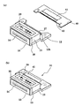
An outline of an example of a head chip of such an ink jet head is shown in FIG. 13, and a cross section of the main part is shown in FIG. As shown in FIGS. 13 and 14, a plurality of
[0004]
A
[0005]
In addition, a
[0006]
A
[0007]
In the head chip configured as described above, when each
[0008]
For example, as shown in FIG. 15, when ink is ejected from the
[0009]
[Problems to be solved by the invention]
In such a head chip, the length of time until the pressure of the ink in the chamber becomes zero and the next ink can be ejected after the side wall vibration due to the ink ejection stops is the length of the chamber or the shape of the nozzle opening. Although it differs depending on the above, since the sealing degree of the chamber is low, it takes time until the sound pressure is repeatedly reflected in the chamber and completely attenuated. Therefore, there is a problem that it is difficult to increase the speed of continuous ejection, that is, to increase the speed of printing.
[0010]
Further, since the time until the sound pressure is attenuated greatly varies depending on the shape of the nozzle opening, there is a problem that it is very difficult to control the discharge amount by the shape of the nozzle opening.
[0011]
Further, the chamber is composed of a boundary portion communicating with the common ink chamber and a pump portion from the nozzle opening driven to discharge ink to the boundary portion, and the length of the pump portion, that is, from the nozzle opening to the boundary portion. The convergence time at which the pressure in the chamber attenuates is determined depending on the distance. However, if the pump length is shortened in order to shorten the convergence time, there is a problem that the ink ejection characteristics deteriorate and printing is not performed normally.
[0012]
In addition, as a drive electric field generated on the side walls on both sides of the chamber by one discharge, a preliminary drive electric field that temporarily increases the volume in the chamber, and a volume in the chamber that is continuous with the preliminary drive electric field are temporarily The ratio of the drive time between the preliminary drive electric field and the discharge drive electric field is a ratio determined by AP to 2N × AP (N is a natural number, AP is a pump length and a pressure propagation speed transmitted through the ink). Time, that is, the time taken from the peak of positive pressure to the peak of negative pressure). This is because the preliminary discharge drive generates a negative pressure in the chamber, and the discharge drive electric field generates a positive pressure in the chamber. However, after the positive pressure is generated by the discharge drive electric field, the volume in the chamber is restored. As a result, after the negative pressure is generated in the chamber and the discharge drive electric field is generated, the positive pressure peak generated after 2N × AP is canceled by the negative pressure to prevent ink leakage and discharge failure.
[0013]
From this, the ratio of the drive time between the preliminary drive electric field and the discharge drive electric field is AP vs. (2N-1) × AP, that is, when the discharge drive electric field is an odd multiple, after the discharge drive electric field is applied, the AP time elapses. The timing of the negative pressure peak generated in the cycle 2AP coincides with the timing of the generation of the negative pressure due to the return of the volume in the chamber, and the negative pressure becomes abnormally large, so that bubbles are mixed in the chamber and the discharge performance is deteriorated. As the ratio of the drive time between the preliminary drive electric field and the discharge drive electric field is AP to 2N × AP, the positive pressure peak generated in the period 2AP after the 2AP time has elapsed after the application of the discharge drive electric field is applied to the chamber. The amount of the negative pressure is offset by the generation of the negative pressure due to the return to the original volume. The time required for the discharge in the preliminary drive electric field and the discharge drive electric field is at least 3AP, the discharge time becomes long, and the time for the pressure in the chamber to converge for the next discharge is also required. There is a problem that it is particularly difficult to increase the speed.
[0014]
In view of such circumstances, the present invention provides an ink jet recording apparatus capable of shortening the convergence time during which the pressure in the chamber is attenuated without deteriorating the ink discharge characteristics, and shortening the driving time to increase the printing speed. It is an object to provide a recording method.
[0015]
[Means for Solving the Problems]
A first aspect of the present invention that solves the above problem is a head chip having a chamber defined in a substrate and having a longitudinal end portion communicating with a nozzle opening, and an electrode provided on a side wall of the chamber; Driving means for generating a driving electric field on the side wall by applying a driving voltage to the electrodes of the head chip to change a volume in the chamber and discharging ink filled therein from the nozzle openings; In the ink jet recording apparatus provided, an ink chamber plate defining a common ink chamber communicating with the chamber is joined to the substrate, and the common ink chamber partitions the chamber and the common ink chamber. The partition is provided with a communication hole that defines a pump length according to a distance from the nozzle opening. The communication hole extends in the longitudinal direction of the chamber. A plurality of the driving means are provided at intervals equal to the length of the head, and the driving means continuously increases the volume of the chamber as the driving electric field generated on the side wall, and the preliminary driving electric field continuously. In the ink jet recording apparatus, the volume in the chamber is temporarily reduced so that the drive time is substantially equal to the discharge drive electric field for discharging ink.
[0016]
According to a second aspect of the present invention, there is provided the ink jet recording apparatus according to the first aspect, wherein the partition portion is formed of a separate member.
[0017]
According to a third aspect of the present invention, in the first or second aspect, the substrate is formed of a piezoelectric ceramic plate, and the chamber is defined by forming a groove in the piezoelectric ceramic plate. The inkjet recording apparatus is characterized in that the common ink chamber communicates with an opening on one side of the chamber in the longitudinal direction opposite to the substrate.
[0018]
According to a fourth aspect of the present invention, in the first or second aspect, the side wall made of piezoelectric ceramic is disposed on the substrate at a predetermined interval to define the chamber on the side wall and In the ink jet recording apparatus, the common ink chamber is defined, and the chamber and the common ink chamber communicate with each other at one longitudinal end of the chamber.
[0019]
According to a fifth aspect of the present invention, there is provided a substrate in which a chamber whose longitudinal end communicates with a nozzle opening is defined and an electrode is provided on a side wall of the chamber, and the chamber bonded to the substrate. The volume of the chamber is changed by applying a voltage to the electrode of the head chip that includes an ink chamber plate that defines a common ink chamber that communicates with the ink, and the ink filled therein is discharged from the nozzle opening. In the ink jet recording method to be ejected, the common ink chamber is provided with a plurality of communication holes defining a pump length by a distance from the nozzle opening at intervals equal to the pump length in the longitudinal direction of the chamber. A preliminary driving electric field that temporarily increases the volume in the chamber as the driving electric field, and a volume in the chamber that is continuous with the preliminary discharge electric field. In an ink jet recording method characterized by generating a discharge electric field to reduce a time to the side walls at a substantially equal driving time.
[0020]
In the present invention, by providing the communication hole that defines the pump length of the chamber, the time during which the pressure in the chamber is attenuated can be shortened without deteriorating the ink supply characteristics and the ink discharge characteristics, and the discharge drive electric field can be reduced. The generation time can be shortened and the drive time associated with ejection can be shortened, and ink can be ejected continuously at high speed to achieve high-speed printing.
[0021]
DETAILED DESCRIPTION OF THE INVENTION
Hereinafter, the present invention will be described in detail based on embodiments.
[0022]
(Embodiment)
1 is an exploded perspective view of an inkjet head according to an embodiment, FIG. 2 is an exploded perspective view of a head chip, and FIG. 3A is a longitudinal sectional view of a chamber of the head chip. 3B is a cross-sectional view taken along the line AA ′ of FIG. 3A, and FIG. 4 is a schematic perspective view showing an assembly process of the ink jet head.
[0023]
As shown in FIG. 1, the
[0024]
First, the
[0025]
Here, each
[0026]
An
[0027]
In the present embodiment, each
[0028]
The
[0029]
Between the piezoelectric
[0030]
Of the plurality of communication holes 31 provided in the
[0031]
The plurality of communication holes 31 are provided at equal intervals, and this interval is the distance between the
[0032]
Here, the pump length of the
[0033]
Therefore, in this embodiment, the
[0034]
Specifically, in the present embodiment, when the length of the
[0035]
For this reason, the distance from the
[0036]
In the present embodiment, the
[0037]
In addition, a
[0038]
In the present embodiment, the
[0039]
In the present embodiment, the
[0040]
In the
[0041]
Further, the
[0042]
As shown in FIGS. 1 and 4, the
[0043]
Further, as shown in FIG. 4A, the
[0044]
In such an
[0045]
Further, such an
[0046]
An example of the
[0047]
Therefore, the
[0048]
The
[0049]
As shown in FIG. 6, the
[0050]
The above-described
[0051]
According to such an ink
[0052]
Here, a driving method of the ink jet recording apparatus will be described in detail.
[0053]
FIG. 7 is a cross-sectional view of a pulse waveform and a piezoelectric ceramic plate showing a driving voltage and a driving signal applied to the side wall of the head chip.
[0054]
As shown in FIG. 7, in the
[0055]
The drive electric field generated on both
[0056]
The drive times of the preliminary drive electric field and the discharge drive electric field were made substantially equal.
[0057]
Specifically, the drive time of the preliminary drive electric field and the ejection drive electric field is expressed as the pulse width of the
[0058]
The drive times of the preliminary drive electric field and the discharge drive electric field, that is, the widths of the B region and the C region of the
[0059]
Here, the movement of the
[0060]
First, when an ink droplet is ejected from the
[0061]
The
[0062]
That is, when the ink droplets are ejected from the
[0063]
FIG. 8 shows the movement of the
[0064]
First, in the region A of the
[0065]
Next, in the region B which is the preliminary driving electric field of the
[0066]
Next, in the region C, which is the ejection driving electric field of the
[0067]
Thereafter, when the region C, which is the ejection driving electric field of the
[0068]
Further, the drive time of the preliminary drive electric field and the discharge drive electric field is determined by the natural number times AP, which is a periodic time obtained from the length of the
[0069]
In the present embodiment, the
[0070]
As shown in the figure, the
[0071]
A plurality of sealing
[0072]
The
[0073]
Furthermore, the
[0074]
Also in such a
[0075]
In the above-described embodiment, the head chip using the insulating ink is exemplified. However, the head chip using the conductive ink such as water-based ink may be used.
[0076]
When conductive ink such as water-based ink is used for the head chip in this way, the electrode is conducted by the ink in the
[0077]
Such an example is shown in FIG. FIG. 11 is an exploded perspective view showing another example of the head chip of the present invention.
[0078]
As shown in the figure,
[0079]
In the
[0080]
Thus, even in the
[0081]
In the case where conductive ink is used for the
[0082]
In the
[0083]
(Example 1)
In Example 1, the length of the
[0084]
In this example, the nozzle resistance of the
[0085]
(Comparative Example 1)
For comparison, this is an example in which the
[0086]
(Test Example 1)
The convergence time of the pressure in the chamber after ejection was measured by driving the
[0087]
As described above with reference to FIGS. 7 and 8, when the discharge driving electric field becomes zero and the volume in the chamber returns to the original state, a negative pressure is generated in the chamber. This is indicated by the E region in FIG. 12, and in Comparative Example 1, it is indicated by the F region in FIG.
[0088]
As described above, the timing for returning the both side walls of the chamber to the original state, that is, the timing for generating the negative pressure is determined by the difference in the driving time of the ejection driving electric field, but the positive pressure generated periodically after the ejection driving electric field is generated. If the negative pressure generation timing that cancels the peak of the pressure does not need to cancel the negative pressure peak and the positive pressure peak that occur periodically due to the rapid convergence of the pressure in the chamber, the next ink droplet can be ejected. The time for the pressure in the chamber to converge is shortened.
[0089]
From the result shown in FIG. 12, when the pressure in the chamber converges, here, the pressure in the chamber at which the next ink droplet can be ejected is defined as ± 10 kPa or less, It can be seen that the
[0090]
Thus, it can be seen that the discharge time in the chamber during the single discharge is reduced by about 8 μs in the
[0091]
Note that such a reduction in the drive time of the discharge drive electric field can be achieved by the generation of negative pressure when the volume in the chamber after discharge is restored and the generation of the discharge drive electric field in the conventional head chip without the
[0092]
In addition, the ink droplet ejection speeds of No. 30, No. 222, and No. 480 were measured with arbitrary nozzle openings in Example 1 and Comparative Example 1, and in this test example, with a total of 510 nozzles. The results are shown in Table 1.
[0093]
[Table 1]
[0094]
In this way, by driving the preliminary drive electric field and the discharge drive electric field with substantially the same drive time, in the first embodiment, the ink droplet discharge speed can be driven without changing from the discharge speed based on the conventional drive timing. The time required can be shortened, and the convergence time of the chamber pressure after ejection can be shortened, so that the speed of continuous ejection, that is, the speed of printing can be increased.
[0095]
In Example 1 and Comparative Example 1, the preliminary driving electric field is 1AP and the ejection driving electric field is 1AP or 2AP. However, this is a case where the shortest ejection time is used. In Example 1, it goes without saying that the drive times of the preliminary drive electric field and the discharge drive electric field may be substantially equal.
[0096]
【The invention's effect】
As described above, in the present invention, the pump length is defined by the distance from the nozzle opening in the partition portion of the common ink chamber, and a plurality of communication holes are provided at intervals of the pump length along the longitudinal direction of the chamber. Convergence time during which the pressure in the chamber decays can be shortened, and the drive time associated with ejection can be shortened by substantially equalizing the drive time of the preliminary drive electric field and the discharge drive electric field, thereby increasing the speed of continuous ejection. That is, the printing speed can be increased. Further, since the time until the sound pressure is attenuated is not affected by the shape of the nozzle opening, control of the discharge amount by the shape of the nozzle opening can be achieved under a certain discharge condition.
[Brief description of the drawings]
FIG. 1 is an exploded perspective view of an inkjet head according to an embodiment of the present invention.
FIG. 2 is an exploded perspective view of a head chip according to an embodiment of the present invention.
3A and 3B are cross-sectional views of a head chip according to an embodiment of the present invention, in which FIG. 3A is a longitudinal cross-sectional view of a chamber, and FIG. 3B is a cross-sectional view taken along line AA ′ of FIG.
FIG. 4 is a perspective view showing an assembly process of the inkjet head according to the embodiment of the invention.
FIG. 5 is an exploded perspective view schematically showing a head unit according to an embodiment of the invention.
FIG. 6 is a schematic perspective view of an ink jet recording apparatus according to an embodiment of the present invention.
7 is a sectional view of a piezoelectric ceramic plate and a pulse waveform showing a driving voltage and a driving signal applied to a side wall of a head chip according to an embodiment of the present invention. FIG.
FIG. 8 is a cross-sectional view of a piezoelectric ceramic plate showing the movement of a side wall when ejecting ink droplets from a chamber according to an embodiment of the present invention.
FIG. 9 is an exploded perspective view showing another example of a head chip according to an embodiment of the present invention.
10A and 10B are cross-sectional views showing another example of a head chip according to an embodiment of the present invention, in which FIG. 10A is a cross-sectional view in the direction in which the chambers are arranged side by side, and FIG. It is sectional drawing.
FIG. 11 is an exploded perspective view showing another example of a head chip according to an embodiment of the present invention.
12 is a diagram illustrating the behavior of the pressure in the chamber with respect to time after applying the pre-driving electric field from the head chips of Example 1 and Comparative Example 1 of the present invention, and FIG. 12 (b) is an enlarged view of the main part of FIG. is there.
FIG. 13 is an exploded perspective view showing an outline of a conventional head chip.
FIG. 14 is a cross-sectional view showing an outline of a head chip according to a conventional technique.
FIG. 15 is a cross-sectional view showing an outline of a head chip according to a conventional technique.
[Explanation of symbols]
10 Inkjet head
11, 11A, 11B Head chip
12 Base plate
13 Head cover
16 Piezoelectric ceramic plate
16A board
17, 17a, 17b, 17c, 17A, 17d Chamber
17e dummy chamber
17p Pump part
18, 18a, 18b, 18A side wall
19, 19a, 19b, 19c, 19A Electrode
20 Ink chamber plate
21 Common ink chamber
21a First ink chamber
21b Second ink chamber
22 Ink supply port
23 Nozzle plate
24 Nozzle opening
30, 30A, 30B Partition
31, 31a, 31b, 31c, 31d Communication hole
32 Ink supply communication hole
40 Wiring board
41 Drive circuit
50 head units
70 Inkjet recording device
Claims (5)
前記基板上には、前記チャンバに連通する共通インク室を画成するインク室プレートが接合されており、前記共通インク室は前記チャンバと前記共通インク室とを仕切る仕切部を具備すると共に該仕切部には前記ノズル開口からの距離によりポンプ長を規定する連通孔が前記チャンバの長手方向に亘って前記ポンプ長と同等の間隔で複数設けられており、前記駆動手段は前記側壁に発生させる前記駆動電界として前記チャンバ内の容積を一時的に増加させる予備駆動電界と、該予備駆動電界に連続して前記チャンバ内の容積を一時的に減少させることでインクを吐出させる吐出駆動電界との駆動時間が略同等となるように駆動することを特徴とするインクジェット式記録装置。By applying a drive voltage to the head chip having a chamber defined in the substrate and having a longitudinal end communicating with the nozzle opening, an electrode provided on a side wall of the chamber, and the electrode of the head chip An ink jet recording apparatus comprising: a driving unit that generates a driving electric field on the side wall to change a volume in the chamber and discharges ink filled therein from the nozzle opening;
An ink chamber plate that defines a common ink chamber that communicates with the chamber is joined to the substrate, and the common ink chamber includes a partition that partitions the chamber and the common ink chamber, and the partition. The part is provided with a plurality of communication holes defining the pump length by the distance from the nozzle opening at the same interval as the pump length in the longitudinal direction of the chamber, and the driving means is generated on the side wall. Driving with a preliminary driving electric field that temporarily increases the volume in the chamber as a driving electric field, and an ejection driving electric field that discharges ink by temporarily decreasing the volume in the chamber continuously with the preliminary driving electric field An ink jet recording apparatus that is driven so that time is substantially equal.
前記共通インク室には前記ノズル開口からの距離によりポンプ長を規定する連通孔が前記チャンバの長手方向に亘って前記ポンプ長と同等の間隔で複数設けられており、前記駆動電界として前記チャンバ内の容積を一時的に増加させる予備駆動電界と、該予備吐出電界に連続して前記チャンバ内の容積を一時的に減少させる吐出電界とを略同等の駆動時間で側壁に発生させることを特徴とするインクジェット式記録方法。A chamber whose longitudinal end communicates with the nozzle opening is defined, and a substrate provided with an electrode on the side wall of the chamber, and a common ink chamber joined to the chamber and communicated with the chamber are defined. In an ink jet recording method in which the volume of the chamber is changed by applying a voltage to the electrode of the head chip including the ink chamber plate, and the ink filled therein is ejected from the nozzle opening.
The common ink chamber is provided with a plurality of communication holes that define the pump length by the distance from the nozzle opening at the same interval as the pump length in the longitudinal direction of the chamber. A pre-driving electric field that temporarily increases the volume of the gas and a discharge electric field that temporarily reduces the volume in the chamber continuously to the pre-discharge electric field are generated on the side wall in substantially the same driving time. An ink jet recording method.
Priority Applications (3)
| Application Number | Priority Date | Filing Date | Title |
|---|---|---|---|
| JP2001369915A JP3730165B2 (en) | 2001-12-04 | 2001-12-04 | Inkjet recording apparatus and recording method |
| GB0227477A GB2382799B (en) | 2001-12-04 | 2002-11-25 | Ink jet recording apparatus and recording method |
| US10/306,691 US6773085B2 (en) | 2001-12-04 | 2002-11-27 | Ink jet recording apparatus and recording method |
Applications Claiming Priority (1)
| Application Number | Priority Date | Filing Date | Title |
|---|---|---|---|
| JP2001369915A JP3730165B2 (en) | 2001-12-04 | 2001-12-04 | Inkjet recording apparatus and recording method |
Publications (2)
| Publication Number | Publication Date |
|---|---|
| JP2003170585A JP2003170585A (en) | 2003-06-17 |
| JP3730165B2 true JP3730165B2 (en) | 2005-12-21 |
Family
ID=19179228
Family Applications (1)
| Application Number | Title | Priority Date | Filing Date |
|---|---|---|---|
| JP2001369915A Expired - Fee Related JP3730165B2 (en) | 2001-12-04 | 2001-12-04 | Inkjet recording apparatus and recording method |
Country Status (3)
| Country | Link |
|---|---|
| US (1) | US6773085B2 (en) |
| JP (1) | JP3730165B2 (en) |
| GB (1) | GB2382799B (en) |
Families Citing this family (3)
| Publication number | Priority date | Publication date | Assignee | Title |
|---|---|---|---|---|
| KR100574017B1 (en) * | 2003-08-11 | 2006-04-26 | 삼성전자주식회사 | An Ink-Cartridge For Ink-Jet Printer |
| GB0510992D0 (en) * | 2005-05-28 | 2005-07-06 | Xaar Technology Ltd | Droplet deposition apparatus |
| JP5768035B2 (en) * | 2012-12-11 | 2015-08-26 | 株式会社東芝 | Pulse generator |
Family Cites Families (6)
| Publication number | Priority date | Publication date | Assignee | Title |
|---|---|---|---|---|
| JPH0246263A (en) | 1988-08-01 | 1990-02-15 | Borden Inc | Manufacture of low water pasta |
| JP3384023B2 (en) * | 1993-04-19 | 2003-03-10 | セイコーエプソン株式会社 | Ink jet recording device |
| DE69504975T2 (en) * | 1994-06-15 | 1999-03-25 | Citizen Watch Co Ltd | METHOD FOR DRIVING AN INK JET PRINT HEAD |
| JP2000037861A (en) * | 1998-07-24 | 2000-02-08 | Brother Ind Ltd | Ink-jet recording apparatus |
| JP4515584B2 (en) * | 1999-04-30 | 2010-08-04 | 東芝テック株式会社 | Capacitive element driving device |
| JP2002326351A (en) * | 2001-04-27 | 2002-11-12 | Sii Printek Inc | Head chip |
-
2001
- 2001-12-04 JP JP2001369915A patent/JP3730165B2/en not_active Expired - Fee Related
-
2002
- 2002-11-25 GB GB0227477A patent/GB2382799B/en not_active Expired - Fee Related
- 2002-11-27 US US10/306,691 patent/US6773085B2/en not_active Expired - Lifetime
Also Published As
| Publication number | Publication date |
|---|---|
| GB2382799A (en) | 2003-06-11 |
| GB2382799B (en) | 2005-03-09 |
| US6773085B2 (en) | 2004-08-10 |
| GB0227477D0 (en) | 2002-12-31 |
| JP2003170585A (en) | 2003-06-17 |
| US20030137565A1 (en) | 2003-07-24 |
Similar Documents
| Publication | Publication Date | Title |
|---|---|---|
| JP2005034997A (en) | Liquid ejection head | |
| EP1236573A2 (en) | Print head chip | |
| JPH05131622A (en) | Ink-jet recording device | |
| JP3730165B2 (en) | Inkjet recording apparatus and recording method | |
| CN112776480B (en) | Liquid ejecting head and liquid ejecting recording apparatus | |
| US6676247B2 (en) | Head chip | |
| EP1752293B1 (en) | Ink jet head driving method, ink jet head and ink jet recording apparatus | |
| JP4146208B2 (en) | Inkjet recording apparatus and inkjet recording method | |
| JPH09226112A (en) | Ink jet recording head | |
| JP3950004B2 (en) | Inkjet recording apparatus and inkjet recording method | |
| JP2004074735A (en) | Head chip, method of manufacturing the same, and inkjet recorder | |
| JP3964262B2 (en) | Head chip | |
| JP7248860B1 (en) | HEAD CHIP, LIQUID JET HEAD AND LIQUID JET RECORDING APPARATUS | |
| JP4694727B2 (en) | Head chip unit and ink jet recording apparatus | |
| JP7220328B1 (en) | HEAD CHIP, LIQUID JET HEAD AND LIQUID JET RECORDING APPARATUS | |
| CN112776481B (en) | Liquid ejecting head and liquid ejecting recording apparatus | |
| JP2018094866A (en) | Liquid jet head and liquid jet recording device | |
| JP3730158B2 (en) | Head chip | |
| JP3669013B2 (en) | Inkjet device | |
| JP3872336B2 (en) | Inkjet recording apparatus and inkjet recording method | |
| JP2007320061A (en) | Liquid droplet discharging apparatus | |
| JPH05318730A (en) | Ink jet head | |
| JPH06328689A (en) | Ink jet printing head | |
| JP4442979B2 (en) | Head chip and head unit | |
| JP2009107164A (en) | Inkjet recorder |
Legal Events
| Date | Code | Title | Description |
|---|---|---|---|
| RD01 | Notification of change of attorney |
Free format text: JAPANESE INTERMEDIATE CODE: A7421 Effective date: 20040309 |
|
| A621 | Written request for application examination |
Free format text: JAPANESE INTERMEDIATE CODE: A621 Effective date: 20040510 |
|
| A977 | Report on retrieval |
Free format text: JAPANESE INTERMEDIATE CODE: A971007 Effective date: 20050915 |
|
| TRDD | Decision of grant or rejection written | ||
| A01 | Written decision to grant a patent or to grant a registration (utility model) |
Free format text: JAPANESE INTERMEDIATE CODE: A01 Effective date: 20051004 |
|
| A61 | First payment of annual fees (during grant procedure) |
Free format text: JAPANESE INTERMEDIATE CODE: A61 Effective date: 20051005 |
|
| R150 | Certificate of patent or registration of utility model |
Ref document number: 3730165 Country of ref document: JP Free format text: JAPANESE INTERMEDIATE CODE: R150 Free format text: JAPANESE INTERMEDIATE CODE: R150 |
|
| FPAY | Renewal fee payment (event date is renewal date of database) |
Free format text: PAYMENT UNTIL: 20091014 Year of fee payment: 4 |
|
| FPAY | Renewal fee payment (event date is renewal date of database) |
Free format text: PAYMENT UNTIL: 20091014 Year of fee payment: 4 |
|
| FPAY | Renewal fee payment (event date is renewal date of database) |
Free format text: PAYMENT UNTIL: 20101014 Year of fee payment: 5 |
|
| FPAY | Renewal fee payment (event date is renewal date of database) |
Free format text: PAYMENT UNTIL: 20101014 Year of fee payment: 5 |
|
| RD03 | Notification of appointment of power of attorney |
Free format text: JAPANESE INTERMEDIATE CODE: R3D03 |
|
| FPAY | Renewal fee payment (event date is renewal date of database) |
Free format text: PAYMENT UNTIL: 20101014 Year of fee payment: 5 |
|
| FPAY | Renewal fee payment (event date is renewal date of database) |
Free format text: PAYMENT UNTIL: 20111014 Year of fee payment: 6 |
|
| FPAY | Renewal fee payment (event date is renewal date of database) |
Free format text: PAYMENT UNTIL: 20111014 Year of fee payment: 6 |
|
| FPAY | Renewal fee payment (event date is renewal date of database) |
Free format text: PAYMENT UNTIL: 20121014 Year of fee payment: 7 |
|
| FPAY | Renewal fee payment (event date is renewal date of database) |
Free format text: PAYMENT UNTIL: 20121014 Year of fee payment: 7 |
|
| FPAY | Renewal fee payment (event date is renewal date of database) |
Free format text: PAYMENT UNTIL: 20131014 Year of fee payment: 8 |
|
| R250 | Receipt of annual fees |
Free format text: JAPANESE INTERMEDIATE CODE: R250 |
|
| R250 | Receipt of annual fees |
Free format text: JAPANESE INTERMEDIATE CODE: R250 |
|
| R250 | Receipt of annual fees |
Free format text: JAPANESE INTERMEDIATE CODE: R250 |
|
| R250 | Receipt of annual fees |
Free format text: JAPANESE INTERMEDIATE CODE: R250 |
|
| LAPS | Cancellation because of no payment of annual fees |