JP3700419B2 - Radiation image processing device - Google Patents
Radiation image processing device Download PDFInfo
- Publication number
- JP3700419B2 JP3700419B2 JP30139198A JP30139198A JP3700419B2 JP 3700419 B2 JP3700419 B2 JP 3700419B2 JP 30139198 A JP30139198 A JP 30139198A JP 30139198 A JP30139198 A JP 30139198A JP 3700419 B2 JP3700419 B2 JP 3700419B2
- Authority
- JP
- Japan
- Prior art keywords
- image data
- image
- defect
- radiation
- defect information
- Prior art date
- Legal status (The legal status is an assumption and is not a legal conclusion. Google has not performed a legal analysis and makes no representation as to the accuracy of the status listed.)
- Expired - Fee Related
Links
- 230000005855 radiation Effects 0.000 title claims description 107
- 238000012545 processing Methods 0.000 title claims description 34
- 230000007547 defect Effects 0.000 claims description 214
- 238000001514 detection method Methods 0.000 claims description 72
- 238000012937 correction Methods 0.000 claims description 51
- 238000000034 method Methods 0.000 claims description 15
- 230000001678 irradiating effect Effects 0.000 claims description 7
- 230000002950 deficient Effects 0.000 description 26
- 238000010586 diagram Methods 0.000 description 15
- 238000003384 imaging method Methods 0.000 description 8
- 239000003990 capacitor Substances 0.000 description 6
- OAICVXFJPJFONN-UHFFFAOYSA-N Phosphorus Chemical compound [P] OAICVXFJPJFONN-UHFFFAOYSA-N 0.000 description 5
- BUGBHKTXTAQXES-UHFFFAOYSA-N Selenium Chemical compound [Se] BUGBHKTXTAQXES-UHFFFAOYSA-N 0.000 description 2
- 238000007599 discharging Methods 0.000 description 2
- 230000000694 effects Effects 0.000 description 2
- 238000009499 grossing Methods 0.000 description 2
- 230000012447 hatching Effects 0.000 description 2
- 229910052711 selenium Inorganic materials 0.000 description 2
- 239000011669 selenium Substances 0.000 description 2
- WUPHOULIZUERAE-UHFFFAOYSA-N 3-(oxolan-2-yl)propanoic acid Chemical compound OC(=O)CCC1CCCO1 WUPHOULIZUERAE-UHFFFAOYSA-N 0.000 description 1
- 238000012935 Averaging Methods 0.000 description 1
- 230000002159 abnormal effect Effects 0.000 description 1
- 238000010521 absorption reaction Methods 0.000 description 1
- 229910052980 cadmium sulfide Inorganic materials 0.000 description 1
- 238000006243 chemical reaction Methods 0.000 description 1
- 150000001875 compounds Chemical class 0.000 description 1
- 238000012217 deletion Methods 0.000 description 1
- 230000037430 deletion Effects 0.000 description 1
- 238000002059 diagnostic imaging Methods 0.000 description 1
- 201000010099 disease Diseases 0.000 description 1
- 208000037265 diseases, disorders, signs and symptoms Diseases 0.000 description 1
- 230000005284 excitation Effects 0.000 description 1
- 230000001747 exhibiting effect Effects 0.000 description 1
- 229910000464 lead oxide Inorganic materials 0.000 description 1
- 230000003902 lesion Effects 0.000 description 1
- 238000004020 luminiscence type Methods 0.000 description 1
- 229960003671 mercuric iodide Drugs 0.000 description 1
- YFDLHELOZYVNJE-UHFFFAOYSA-L mercury diiodide Chemical compound I[Hg]I YFDLHELOZYVNJE-UHFFFAOYSA-L 0.000 description 1
- 239000011368 organic material Substances 0.000 description 1
- YEXPOXQUZXUXJW-UHFFFAOYSA-N oxolead Chemical compound [Pb]=O YEXPOXQUZXUXJW-UHFFFAOYSA-N 0.000 description 1
- 230000001360 synchronised effect Effects 0.000 description 1
Images


Description
【0001】
【発明の属する技術分野】
この発明は放射線画像処理装置に関する。
【0002】
【従来の技術】
従来、疾病の診断等のため、放射線画像を得ることができる放射線画像処理装置が知られている。この放射線画像処理装置では、例えば放射線エネルギーの一部を蓄積して、その後可視光等の励起光を照射すると蓄積されたエネルギーに応じて輝尽発光を示す輝尽性蛍光体をシート状とした輝尽性蛍光体シートが用いられる。この輝尽性蛍光体シートを用いる装置では、被写体を透過した放射線を輝尽性蛍光体シートに照射することで被写体の放射線画像情報を記録し、この情報が記録された輝尽性蛍光体シートにレーザ光等を照射して得られる輝尽発光を集光して光電素子で電気信号に変換することにより、この電気信号に基づいて放射線画像の画像データが生成される。さらに、Flat Panel Detector(FPD)と呼ばれる、2次元的に配列された複数の検出素子で照射された放射線の線量に応じた電気信号を生成し、この電気信号に基づいて画像データが生成される装置も使用される。
【0003】
【発明が解決しようとする課題】
ところで、複数の検出素子が2次元的に配列されているFPDでは、照射された放射線の線量に対する電気信号の信号レベル(信号値)が全ての検出素子で均一ではなく、破損した素子や不良な素子など信号レベルが他の検出素子とは異なったレベル、すなわち異常なレベルとなってしまう検出素子(以下「欠陥画素」という)を含む場合がある。このような欠陥画素を含む場合には、FPDから読み出された信号に基づく画像データにおいて画像欠陥が生じてしまうことから、撮影画像から病変等の読影をする際に、その妨げとなってしまう場合が生じてしまう。
【0004】
また、画像欠陥が生じたときに補正を行うものとした場合、補正後の画像データからは補正が行われた位置を判別することができないことから、補正が行われた位置を確認することができなくなってしまう。
【0005】
そこで、この発明では、画像欠陥が生じた場合であっても良好な見やすい放射線画像を得ることができると共に、画像欠陥の位置を容易に判別することができる放射線画像処理装置を提供するものである。
【0006】
【課題を解決するための手段】
この発明に係る放射線画像処理装置は、2次元的に配列された複数の放射線検出素子からの出力信号に基づいて画像データを作成する画像データ作成手段と、画像データ作成手段で作成された第1の画像データを用いて画像欠陥を検出すると共に、検出された画像欠陥の位置を示す欠陥情報を生成する欠陥検出手段と、欠陥検出手段で生成された欠陥情報を記憶する欠陥情報記憶手段と、欠陥情報記憶手段に記憶した欠陥情報に基づき、被写体を透過した放射線を複数の放射線検出素子に照射して作成した第2の画像データの画像欠陥を補正して第3の画像データを作成する欠陥補正手段とを有する放射線画像処理装置であって、第2の画像データと第3の画像データを1つの画像データとして処理する画像データ処理手段を有するものである。
【0007】
また、画像表示手段と、画像表示手段に画像データを供給する画像データ供給手段とを備え、画像データ供給手段では、第2の画像データあるいは第3の画像データのいずれかを切り換えて画像表示手段に供給し、あるいは両方を画像表示手段に供給し、画像表示手段では、画像データ供給手段から供給された画像データに基づく放射線画像を表示するものである。
【0008】
また、画像データを出力する画像データ出力手段とを備え、画像データ出力手段では、第2の画像データ及び第3の画像データの両方の画像データを1枚の媒体に出力可能となるよう処理して出力するものである。
【0009】
この発明においては、画像欠陥の補正が行われる前の画像データと補正が行われた後の画像データが対として処理されて、この対とされた画像データに基づき補正前の放射線画像と補正後の放射線画像が同時にあるいは切り換えて表示される。また、対とされた画像データがまとめて出力される。さらに補正前の画像データあるいは補正後の画像データに代えて、画像欠陥の位置を示す情報が用いられて、画像欠陥の位置を示す表示あるいは画像欠陥の位置を示す情報の出力が行われる。ここで、例えば放射線画像を表示する表示手段の画素数が表示する画像データの画素数よりも少ない場合には、画像欠陥が最も少なくなるように画像データの間引きが行われる。また、画像データを1枚の媒体に放射線画像として出力する外部機器において、1枚の媒体に対して出力できる画素数が、画像データの画素数よりも少ない場合には、この外部機器に応じて画像欠陥が最も少なくなるように間引きを行った画像データが放射線画像処理装置から外部機器に出力される。
【0010】
【発明の実施の形態】
次に、この発明の実施の一形態について図を用いて詳細に説明する。図1は、放射線画像処理装置の構成を示す図である。放射線発生装置10はコントローラ40によって制御される。この放射線発生装置10から放射された放射線は、被写体5を通して放射線画像読取装置20の撮像パネルに照射される。放射線画像読取装置20では、照射された放射線の強度に基づく画像データを生成する。コントローラ40では、放射線画像読取装置20で生成された画像データを用いて、放射線画像の処理や表示あるいは記録等を行う。
【0011】
図2は、放射線画像読取装置20の構成を示している。この放射線画像読取装置20では、照射された放射線の線量に応じて電気信号を出力する検出素子DT-(1,1)〜DT-(m,n)が2次元配置されて撮像パネル22が構成されている。
【0012】
ここで、検出素子DTは、照射された放射線の線量に応じた電気信号を出力するものであれば良い。例えば放射線が照射されたときに電子−正孔対が生成されて抵抗値が変化する光導電層を用いて検出素子が形成されている場合、この光導電層で生成された放射線量に応じた量の電荷が電荷蓄積コンデンサに蓄えられて、この電荷蓄積コンデンサに蓄えられた電荷を電気信号として出力する。なお、光導電層としては暗抵抗値が高いものが望ましく、アモルファスセレン、酸化鉛、硫化カドミウム、ヨウ化第2水銀、または光導電性を示す有機材料(X線吸収コンパウンドが添加された光伝導性ポリマを含む)などが用いられ、特にアモルファスセレンが望ましい。
【0013】
また、検出素子DTが、例えば放射線が照射されることにより蛍光を生ずるシンチレータ等を用いて形成されている場合、フォトダイオードにおいて、このシンチレータで生じた蛍光強度に基づく電気信号を生成して信号選択部25に供給するものとしてもよい。なお、シンチレータとしては、Gd2O2S:Tb、MX:Tl(M=Rb、Cs:X=Cl、Br、I)、BaFX:Eu(X=Cl、Br、I)、LaOBr:A(A=Tb、Tm)、YTaO4、〔Y,Sr〕TaO4:Nb、CaWO4などが用いられ、特にGd2O2S:Tb、CsI:Tl、BaFCl:Euが望ましい。
【0014】
撮像パネル22の検出素子DT間には、走査線222-1〜222-mと信号線224-1〜224-nが例えば直交するように配設される。この走査線222-1〜222-mは走査駆動部24と接続されており、走査駆動部24では後述する読取制御部27から供給された制御信号CTAに基づき読出信号RSを生成して走査線222-1〜222-mのうちの1つ走査線222-p(pは1〜mのいずれかの値)に出力する。また信号線224-1〜224-nには電荷検出部226-1〜226-nが接続されており、電荷検出部226-1〜226-nでは、検出素子DTから読み出した電荷の電荷量に応じた電圧信号SVを生成する。
【0015】
ここで、読出信号RSによって、走査線222-pに接続された検出素子DT-(p,1)〜DT-(p,n)から、照射された放射線の線量に応じて電荷蓄積コンデンサに蓄積された電荷が読み出されると、電荷検出部226-1〜226-nでは、読み出した電荷の電荷量に応じた電圧信号SV-1〜SV-nを生成する。この電荷検出部226-1〜226-nで生成された電圧信号SV-1〜SV-nは信号選択部25に供給される。
【0016】
信号選択部25は、複数のレジスタ25aを用いて構成されており、電荷検出部226-1〜226-nがレジスタ25aの数に応じて区分されて、1つのレジスタには隣接する所定の数の電荷検出部から電圧信号が供給される。各レジスタ25aにはA/D変換器25bが接続されており、レジスタ25aでは、後述する読取制御部27からの制御信号CTBに基づき、供給された電圧信号SVを順次選択してA/D変換器25bに供給することにより、例えば12ビットないし14ビットのディジタルの画像データSDを生成する。この信号選択部25で生成された1画像分の画像データSD-(1,1)〜SD-(m,n)は、読取制御部27を介してコントローラ40に供給される。
【0017】
なお、撮像パネル22の検出素子DTを複数のブロックに分割して、各ブロックで並列して画像データを生成するものとすれば、1画像分の画像データSD-(1,1)〜SD-(m,n)を速やかに得ることができる。
【0018】
読取制御部27には、コントローラ40が接続されており、読取制御部27ではコントローラ40からの制御信号MCAに基づき、放射線発生装置10での動作と同期して各種の制御信号、例えば放射線照射前に撮像パネル22の電荷蓄積コンデンサに蓄えられている電荷を排出させるための初期化動作や、撮像パネル22に照射された放射線に基づき電荷蓄積コンデンサに蓄えられた電荷を読み出して画像データSDを生成する処理等を行うための制御信号CTA,CTBを生成する。
【0019】
図3はコントローラ40の構成を示しており、コントローラ40の動作を制御するためのCPU(Central Processing Unit)41には、システムバス42と画像バス43が接続される。なお、コントローラ40の動作を制御するためのCPU41は、メモリ44に記憶された制御プログラムに基づいて動作制御を行う。
【0020】
システムバス42と画像バス43には、メモリ44、撮影制御部46、画像メモリ制御部48、表示制御部55、ディスク制御部61、出力インタフェース60が接続されると共に、システムバス42には欠陥検出部50と欠陥補正部52が接続されており、システムバス42を利用してCPU41によって各部の動作が制御されると共に、画像バス43を介して各部間での画像データの転送等が行われる。また、撮影制御部46を介して放射線発生装置10での放射線の照射や放射線画像読取装置20での放射線画像の読み取りの制御が行われる。
【0021】
放射線画像読取装置20から供給された1画像分の画像データSDは、撮影制御部46や画像メモリ制御部48を介して画像メモリ49に記憶される。この画像メモリ制御部48には、欠陥検出部50と欠陥補正部52が接続されており、欠陥検出部50では、画像メモリ49に書き込まれている画像データSDを用いて、検出素子からの電気信号の信号レベルが他の検出素子とは異なるレベルとなる検出素子の検出、すなわち画像欠陥の検出を行う。ここで、欠陥検出部50で画像欠陥を検出したときには、画像欠陥の位置を示す情報FDを生成してメモリ44の欠陥情報記憶領域44aに記憶する。
【0022】
欠陥補正部52では、放射線を被写体に照射して作成された画像データSDが画像メモリ49に書き込まれたときには、メモリ44の欠陥情報記憶領域44aに記憶されている画像欠陥の位置を示す情報FDを用いて、画像メモリ49の画像欠陥の画像データの補正を行い、新たな1画像分の画像データを生成して画像メモリ49に記憶する。
【0023】
画像メモリ49に記憶された画像データは、読み出されて表示制御部55やディスク制御部61に供給される。
【0024】
表示制御部55には画像表示装置56が接続されており、この画像表示装置56の画面上には表示制御部55に供給された画像データやメモリ44の欠陥情報記憶領域44aに記憶された情報に基づき、例えば画像欠陥の補正前後の放射線画像や画像欠陥の位置が表示される。
【0025】
また、放射線画像読取装置20の画素数よりも画像表示装置56の表示画素数が少ない場合には、CPU41によって画像データの間引きを行うことにより、画像表示装置56の画面上に撮影画像全体を表示させることができる。また、画像表示装置56の表示画素数分に相当する領域の画像データを読み出すものとすれば、所望の位置の撮影画像を詳細に表示させることができる。
【0026】
画像メモリ49からディスク制御部61に画像データを供給する際には、例えば連続して画像データを読み出してディスク制御部61内のFIFOメモリに書き込み、その後順次ディスク装置62に記録する。
【0027】
さらに、画像メモリ49から読み出された画像データやディスク装置62から読み出された画像データを出力インタフェース60を介して外部機器100に供給することもできる。この外部機器100では、供給された画像データを例えば1枚のフィルムなどの媒体に放射線画像として出力する。
【0028】
また、CPU41には入力インタフェース63を介してキーボード等の入力装置64が接続されており、入力装置64を操作することで放射線画像の撮影や処理等が行われる。
【0029】
このコントローラ40で画像データの複写や転送、削除等の処理を行う場合、放射線画像読取装置20から供給された補正前の画像データと、欠陥補正部52で画像欠陥の補正が行われた新たな1画像分の画像データを対として処理する。
【0030】
なお、上述の実施の形態では、コントローラ40で放射線発生装置10と放射線画像読取装置20の動作を制御するものとしたが、放射線画像読取装置20の動作を放射線発生装置10に同期させるものとし、放射線画像読取装置20で画像データが得られたときに、この画像データをコントローラ40に供給するものとしても良いことは勿論である。
【0031】
次に動作について説明する。放射線画像の撮影を行う場合、放射線未照射画像データSDAや放射線一様照射画像データSDBあるいは放射線被写体照射画像データSDCを放射線画像読取装置20からコントローラ40に供給するものとして、コントローラ40の欠陥検出部50で画像欠陥の検出を行う。
【0032】
ここで、放射線未照射画像データSDAは、撮像パネル22の初期化動作、すなわち検出素子DTの電荷蓄積コンデンサに蓄えられている電荷を排出させる動作を実施した後に、放射線未照射状態で生成された画像データである。また、放射線一様照射画像データSDBは、初期化動作を実施し放射線を一様に照射してから生成された画像データであり、放射線被写体照射画像データSDCは、初期化動作を実施した後に被写体を透過させて放射線を照射してから生成された画像データである。
【0033】
この画像欠陥の検出では、放射線未照射画像データSDAや放射線一様照射画像データSDBあるいは放射線被写体照射画像データSDCのいずれか1種類の画像データを用いて画像欠陥の検出を行っても良く、また複数種類の画像データを用いて画像欠陥の検出を行っても良い。さらに、画像データとして放射線未照射画像データSDA、放射線一様照射画像データSDBのいずれか1つあるいは両方の画像データを用いることが望ましい。
【0034】
図4は第1の画像欠陥の検出方法を説明するための図である。図4Aは、画像メモリ49に書き込まれている1画像分の画像データを示しており、この画像メモリ49から例えば横方向に画像データを順次読み出し、図4Bに示すように、しきい値TAH,TALと比較して画像欠陥の検出が行われる。
【0035】
しきい値TAH,TALは例えば図5に示すように画像データのヒストグラムに基づいて設定される。正常な画像データの分布が図5の斜線部で示すような分布となる場合、低レベル側しきい値TALは正常な画像データの分布よりも低レベル側に設定されると共に、高レベル側しきい値TAHは正常な画像データの分布よりも高レベル側に設定される。ここで、画像データのレベルが高レベル側しきい値TAHよりも大きくなる画素P(a,ba)や低レベル側しきい値TALよりも小さくなる画素P(a,bb)は、画像欠陥を生ずる欠陥画素と判別されて、画素P(a,ba),P(a,bb)の位置情報が画像欠陥の位置を示す情報としてメモリ44の欠陥情報記憶領域44aに記憶される。
【0036】
図6は画像欠陥の第2の検出方法を説明するための図である。図6Aは、画像メモリ49に書き込まれている1画像分の画像データを示しており、欠陥画素が生ずるか否かの判別が行われる画素P(c,d)に対して、例えば図6Bの斜線で示す周辺の8画素の画像データの平均レベルMD(c,d)を求め、画素P(c,d)の画像データSD(c,d)が平均レベルMD(c,d)に対して所定範囲内(MD(c,d)−W〜MD(c,d)+W)であるか否かの判別が行われる。ここで、画像データSD(c,d)が所定範囲内(MD(c,d)−W〜MD(c,d)+W)で無いときには画素P(c,d)が画像欠陥を生ずる欠陥画素と判別されて、画像欠陥の位置、すなわち画素P(c,d)の位置を示す情報が欠陥情報記憶領域44aに記憶される。なお、平均レベルを算出するために用いられる画素の画像データは、図6Bの斜線で示す部分の8画素に限られるものでなく、例えばハッチングで示す部分を含めた24画素の画像データ等を用いても良い。また、「W」はもともとの画像データがもつレベル変動(ノイズなどに依存する)を検出せずに画像欠陥を検出する範囲で、任意に決めることができる。
【0037】
ところで、上述の第1および第2の画像欠陥の検出方法では、1画素毎に画像欠陥であるか否かを判別するものであるが、欠陥画素と正常画素の画像データのレベル差が大きくない場合には、レベル差が正常画素の画像データのレベル変動であるか画像欠陥であるか判別することが困難である。そこで、画像欠陥がライン状であるときには、欠陥画素と正常画素の画像データのレベル差が大きくない場合であっても画像欠陥を検出できる方法を第3の画像欠陥の検出方法として説明する。
【0038】
図7は第3の画像欠陥の検出方法を説明するための図である。図7Aは、画像メモリ49に書き込まれている1画像分の画像データを示しており、この1画像分の画像データから、縦方向あるいは横方向に隣接する複数ライン分の画像データを読み出すことにより、読み出し方向と直交する方向での平均レベルが求められる。この求められた平均レベルが上述の第1の画像欠陥の検出方法と同様にしきい値と比較されて画像欠陥の検出が行われる。
【0039】
例えば、図7Aに示すように横方向のeラインから(e+f)ラインまでの(f+1)ライン分の画像データが画像メモリ49から読み出されて、縦方向の画素列毎の平均レベルが算出されて、図7Bに示すように(f+1)ライン分の画像データを平均した1ラインの画像データが算出される。ここで、画像欠陥が縦方向のライン状である場合、欠陥画素と正常画素の画像データのレベル差が大きくない場合であっても、平均レベルを算出することによって正常画素の画像データのレベル信号の変動分を小さくすることができる。このため、図7Cに示すように1ライン分の画像データでは検出しにくい画素P(e+h,g)の画像欠陥も、(f+1)ライン分の画像データの平均レベルを算出することで、図7Bに示すように画素P(e〜e+f,g)に相当する画像データを正常画素の画像データとは異なるレベルとすることができるので、複数ライン分の画像データの平均レベルに応じて設定された低レベル側しきい値TBLおよび高レベル側しきい値TBHと求められた平均レベルを比較し、求められた平均レベルが設定された低レベル側しきい値TBLから高レベル側しきい値TBHまでの範囲内であるか否かを判別することによって容易にライン状の画像欠陥を検出することができる。
【0040】
また、求められた平均レベルがeラインや(e+f)ラインの周囲の画像データの平均レベルに対して所定範囲内であるか否かによってもライン状の画像欠陥を検出することができる。ここで、画像欠陥と判別されたときには、縦方向に(f+1)行分の画素すなわち画素P(e〜e+f,g)が欠陥画素と判別されて、画素P(e〜e+f,g)の位置を示す情報が欠陥情報記憶領域44aに記憶される。
【0041】
画像メモリ49から読み出される画像データのヒストグラムが広い幅をもち、例えば図8Aに示すように1ラインの放射線被写体照射画像データSDCの信号レベルが広い範囲にある場合、画像メモリ49から読み出された画像データと、しきい値TCLおよびしきい値TCHを比較しただけでは画素P(q,r)の画像欠陥を検出することができない。そこで、被写体に応じた画像データから一様な勾配や低周波成分を除去するトレンド除去を行い、上述の第1〜第3の画像欠陥の検出方法を用いることにより、正しく画像欠陥の検出を行うことができる。
【0042】
このトレンド除去の一例としては、1ライン分の画像データからスムージングを行って高周波成分を除くものとし、元の画像データからスムージングによって得られた画像データを減算あるいは除算することよって、図8Bに示すように低周波成分を除いた高周波成分だけの画像データHSDCが生成される。
【0043】
また、トレンド除去を行った場合には、図5と比較して図9の斜線で示すように正常な画像データのヒストグラムの幅が狭いものとされる。このため、低レベル側しきい値TDLから高レベル側しきい値TDHまでの幅も、トレンド除去を行う前よりも狭く設定することができるので、画像欠陥の検出を精度良く行うことができる。また、画像データHSDCを用いて上述の第2および第3の画像欠陥の検出方法を行うことにより、画像欠陥を検出することができることは勿論である。
【0044】
このようにして、欠陥検出部50で画像欠陥を検出したときには、画像欠陥の位置を示す情報FDをメモリ44の欠陥情報記憶領域44aに記憶する。なお、画像欠陥の検出では、上述の第1〜第3の画像欠陥の検出方法のいずれか1つの方法あるいは複数の検出方法を用いて画像欠陥の検出を行っても良く、更に他の方法を用いるものとしても良いことは勿論である。
【0045】
ここで、欠陥情報記憶領域44aには、画像欠陥の位置を示す情報FDとして例えば画像欠陥を生ずる画素のアドレスを記憶する。また欠陥情報記憶領域44aに、マップ形式で画像欠陥の位置を示す情報FDを記憶するものとしてもよい。すなわち、欠陥情報記憶領域44aとして1画像分の画素と対応する領域を設けるものとし、画像欠陥が検出されたときには、この画像欠陥を生ずる画素の位置と対応する領域内の位置に所定のデータ値を書き込むものとしてもよい。例えば、正常画素の信号レベルを「1」、欠陥画素の信号レベルを「0」などとすることができる。
【0046】
欠陥補正部52では、欠陥情報記憶領域44aに記憶されている画像欠陥の情報FDを読み出して欠陥の位置を判別し、この判別された画像欠陥の画像データの補正を行う。ここで、画像欠陥の位置を示す情報として画像欠陥を生ずる画素のアドレスが記憶されているときには、記憶されたアドレスを順次読み出すことで画像欠陥の位置が判別される。またマップ形式で画像欠陥の位置を示す情報が欠陥情報記憶領域44aに記憶されているときには、領域44a内のデータ値が所定のデータ値であるか否かを順次検出することにより画像欠陥であるか否かを判別することができる。
【0047】
次に、欠陥情報記憶領域44aに画像欠陥の位置を示す情報FDが記憶されているときに、画像メモリ49に放射線被写体照射画像データSDCが書き込まれると、欠陥情報記憶領域44aに記憶された画像欠陥の位置を示す情報FDに基づき画像メモリ49に書き込まれている放射線被写体照射画像データSDCを用いて欠陥補正部52で画像欠陥の位置の画像データの補正を行う。
【0048】
欠陥補正部52では、欠陥情報記憶領域44aに記憶されている画像欠陥の情報FDを読み出して欠陥の位置を判別し、この判別された画像欠陥の画像データの補正を行う。ここで、画像欠陥の位置を示す情報として画像欠陥を生ずる画素のアドレスが記憶されているときには、記憶されたアドレスを順次読み出すことで画像欠陥の位置が判別される。またマップ形式で画像欠陥の位置を示す情報が欠陥情報記憶領域44aに記憶されているときには、メモリ領域内のデータ値が所定のデータ値であるか否かを順次検出することにより画像欠陥であるか否かを判別することができる。
【0049】
この欠陥補正部52で画像欠陥の位置が判別されると、画像欠陥を生ずる画素の周囲の正常画素の画像データを画像メモリ49から読み出し、この読み出した画像データを用いて補正を行う。補正方法の一例として、周囲の正常画素の画像データの平均レベルを欠陥画素の画像データとする、というものがある。図10Aに示すように、画像欠陥を生ずる画素P(s,t)の周囲が正常画素であるときには、画素P(s,t)の上下方向と左右方向に隣接する4画素、あるいは斜線で示す斜め方向に隣接する画素を含めた8画素、またはハッチングで示す部分を含めた24画素の画像データの平均レベルが算出されて、この平均レベルが補正後の画素P(s,t)の画像データとされる。なお、欠陥画素が周囲にある場合には、この欠陥画素を除いた正常画素の画像データのみを用いて補正を行う。
【0050】
また、画像欠陥を補正する場合には、画素P(s,t)からの距離によって画像データの重み付けを行うものとし、重み付けがなされた画像データの平均レベルを補正後の画像データとすることもできる。例えば図10Bに示すように、画素P(s,t)の中心から上下左右の画素の中心までの距離を「1」としたとき斜めの画素の中心までの距離が「√2」であることから、斜めの画素の画像データを(1/√2)倍して重み付けを行い、重み付けがなされた画像データの平均レベルが補正後の画像データとされる。
【0051】
なお、欠陥補正部52での補正方法は、上述の方法に限られるものではなく、例えば『「Restoring Spline Interpolation of CT Images」IEEE TRANSACTION ON MEDICAL IMAGING VOL.MI-2,NO3 SEPTEMBER 1983 、「Cubic Convolution for Digital Image Processing IEEE TRANSACTION ON ACOUSTICS AND SIGNAL PROCESSING VOL.ASSP-29」』に記載されているニアレスト・ネイバー補間、ベルースプライン補間、リニア補間、キュービック・コンボリュージョン補間等によって得られた画像データを補正後の画像データとして用いるものとしてもよい。
【0052】
このようにして得られた補正後の1画像分の画像データは、画像メモリ49に書き込まれている補正前の1画像分の画像データと対として処理する。例えば、画像データの複写や転送等の処理は補正前および補正後の画像データが1つの画像データとして扱われる。また、画像データの消去の際に画像欠陥の補正前の画像データだけを消去する処理を禁止することにより、消去が禁止された画像欠陥の補正前の画像データを用いて、種々の方法で画像欠陥の検出や補正を行って最適な撮影画像を得ることができる。さらに、画像欠陥の補正前の画像データが残されることにより、もともと画像欠陥であった画素の位置がわからなくなってしまうことを防止できる。
【0053】
なお、画像欠陥の検出および画像欠陥の補正は、画像メモリ49に書き込まれた画像データを用いて行われる場合に限られるものではなく、既に撮影された画像データ、例えばディスク装置62に記憶されている画像データ等を画像メモリ49に書き込むものとすれば、上述したように画像欠陥の検出および画像欠陥の補正を行うことで、既に撮影された画像データからも良好な放射線画像を得ることができる。
【0054】
さらに、上述の実施の形態では、欠陥検出部50で自動的に画像欠陥の検出を行い、検出された画像欠陥の位置を示す情報FDを欠陥情報記憶領域44aに記憶するものとしたが、図示しない画像表示装置の画面上に撮影画像を表示させて、ユーザが表示された撮影画像から画像欠陥を検出したときには、この検出された画像欠陥の位置を情報FDとして欠陥情報記憶領域44aに書き込むことができるようにしてもよい。この場合、欠陥検出部50で検出することができない画像欠陥が生じていても画像欠陥の補正を行うことができるので、更に良好な放射線画像を得ることができる。また、画像欠陥の自動検出とユーザが画像欠陥を検出する方法を合わせて行うことものとすれば更に有効である。
【0055】
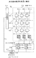
コントローラ40では、対とされた補正前と補正後の各1画像分の画像データを表示制御部55に供給することにより、図11Aに示すように画像表示装置56の画面上に補正前の画像データに基づく放射線画像と補正後の画像データに基づく放射線画像を同時に表示することで、良好な放射線画像を得ることができるだけでなく画像欠陥の位置を確認することができる。なお、補正前の放射線画像と補正後の放射線画像を切り換えて表示すれば、放射線画像を大きく表示することもできる。
【0056】
さらに、欠陥情報記憶領域44aに記憶されている情報を表示制御部55やコントローラ40に供給することにより、図11Bに示すように画像表示装置56の画面上に補正後の画像データに基づく画像と欠陥画素の位置を示す表示を同時に表示しても、良好な放射線画像を得ることができるだけでなく画像欠陥の補正の効果も容易に確認することができる。なお、この場合にも、補正後の放射線画像や欠陥画素の位置を切り換えて表示すれば、放射線画像を大きく表示することができると共に、欠陥画素の位置を容易に確認できる。
【0057】
また、欠陥画素の位置を示す際には、正常な画素を白あるいは黒で表示するものとし、欠陥画素は表示を反転させることで容易に欠陥画素の位置を判別することができる。
【0058】
このように、補正前の撮影画像や欠陥画素の位置を表示可能とすることで、いずれの画素の画像データが補正されたかを容易に確認することができ、医師等は欠陥画素の位置を把握しながら読影を行うことができる。
【0059】
さらに、画像データの間引きを行い撮影画像を画面上に表示する際には、欠陥情報記憶領域44aに記憶されている欠陥情報に基づき、画像欠陥がいずれの位置にあるかを判別して画像欠陥の位置の画像データを除いて放射線画像を表示すれば、補正された画素の数が少なく良好な放射線画像を得ることができる。
【0060】
例えば、100画素×100画素の画像データを(1/10)に間引く場合、1画素目から10画素毎に画像データを用いたときの画像欠陥の欠陥数を判別し、次に2画素目から10画素毎に画像データを用いたときの欠陥数を判別する。以下同様に10画素目から10画素毎に画像データを用いたときの欠陥数を判別し、最も欠陥数が少なくなるように画像データを10画素毎に用いることで、良好な放射線画像を得ることができる。
【0061】
また、画像表示装置56の画面上に複数の画像を表示する場合、例えば補正前の放射線画像と補正後の放射線画像を表示する場合に、画像データの間引きを行うときには、同じ画素位置の画像データを間引いたものを表示する。このように同じ画素位置の画像データを間引くことにより、表示された2つの画像が同じ画素位置の画像データに基づく放射線画像を得ることができるので、画像欠陥の補正した位置を確認することができる。
【0062】
さらに、上述の実施の形態では、画像表示装置56に画像欠陥の補正が行われる前の放射線画像や補正が行われた後の放射線画像を合わせて表示したり画像欠陥の位置を示す表示と補正が行われた後の放射線画像を合わせて表示する場合について説明したが、画像欠陥の補正が行われる前の放射線画像の画像データと補正が行われた後の放射線画像の画像データをコントローラ40から出力インタフェース60を介して外部機器100に供給したり、メモリ44の欠陥情報記憶手段44aに記憶した欠陥情報に基づいて生成した画像欠陥の位置を示す画像データと補正が行われた後の放射線画像の画像データを外部機器100に供給するものとしてもよい。ここで、外部機器100では、供給された画像データを1枚のフイルムなどの媒体に放射線画像として出力する。さらに、画像欠陥の補正が行われる前の放射線画像の画像データや補正が行われた後の放射線画像の画像データあるいは画像欠陥の位置を示す画像データを外部機器100に出力する場合、1枚の媒体に放射線画像を出力可能となるように画像データを処理して出力するものとして良い。すなわち、外部機器100で1枚の媒体に対して出力できる画素数が画像データの画素数よりも少ないときには、同じ画素位置の画像データを外部機器100の出力できる画素数に応じて間引きして出力しても良いことは勿論である。
【0063】
なお、上述の実施の形態では、画像メモリ、欠陥検出部、欠陥補正部および画像表示装置がコントローラ40に設けられている場合について説明したが、これらを放射線画像読取装置20に設けるものとして、放射線画像読取装置側で良好な放射線画像を表示したり、画像欠陥の位置を容易に判別可能とすることもできる。
【0064】
【発明の効果】
この発明によれば、画像欠陥の補正が行われる前の放射線画像の画像データと補正が行われた後の放射線画像の画像データが対として処理されて、放射線画像の表示あるいは画像データの出力が行われるので、補正が行われた位置の確認を容易とすることができる。また、補正前の画像データに代えて、画像欠陥の位置を示す情報が用いられたときにも同様に、補正が行われた位置の確認を容易に行うことができる。さらに画像データを間引きして放射線画像の表示あるいは画像データの出力を行う場合に、画像欠陥が最も少なくなるように間引きが行われるので、間引き後の画像データを用いても補正が行われた画素の少ない良好な放射線画像を得ることができる。
【図面の簡単な説明】
【図1】放射線画像処理装置の構成を示す図である。
【図2】放射線画像読取装置の構成を示す図である。
【図3】コントローラの構成を示す図である。
【図4】第1の欠陥画素検出方法を説明するための図である。
【図5】しきい値の設定方法を説明するための図である。
【図6】第2の欠陥画素検出方法を説明するための図である。
【図7】第3の欠陥画素検出方法を説明するための図である。
【図8】トレンド除去を説明するための図である。
【図9】トレンド除去を行ったときのしきい値の設定方法を説明するための図である。
【図10】欠陥画素の画像データの補正方法を説明するための図である。
【図11】表示画像を示す図である。
【符号の説明】
10 放射線発生装置
20 放射線画像読取装置
22 撮像パネル
24 走査駆動部
25 信号選択部
27 読取制御部
29 パネル駆動部
40 コントローラ
41 CPU(Central Processing Unit)
44 メモリ
44a 欠陥情報記憶領域
48 画像メモリ制御部
49 画像メモリ
50 欠陥検出部
52 欠陥補正部
55 表示制御部
56 画像表示装置[0001]
BACKGROUND OF THE INVENTION
The present invention relates to a radiation image processing apparatus.
[0002]
[Prior art]
Conventionally, a radiological image processing apparatus capable of obtaining a radiographic image for diagnosing a disease or the like is known. In this radiographic image processing apparatus, for example, a part of radiation energy is accumulated, and then when irradiated with excitation light such as visible light, a photostimulable phosphor that exhibits stimulated luminescence according to the accumulated energy is formed into a sheet shape. A photostimulable phosphor sheet is used. In the apparatus using the photostimulable phosphor sheet, radiation image information of the subject is recorded by irradiating the photostimulable phosphor sheet with radiation transmitted through the subject, and the photostimulable phosphor sheet on which this information is recorded The stimulated light emission obtained by irradiating the laser beam or the like is condensed and converted into an electric signal by a photoelectric element, whereby image data of a radiographic image is generated based on the electric signal. Furthermore, an electrical signal corresponding to the radiation dose irradiated by a plurality of two-dimensionally arranged detection elements called Flat Panel Detector (FPD) is generated, and image data is generated based on the electrical signal. A device is also used.
[0003]
[Problems to be solved by the invention]
By the way, in an FPD in which a plurality of detection elements are two-dimensionally arranged, the signal level (signal value) of an electrical signal with respect to the dose of irradiated radiation is not uniform among all detection elements, and a damaged element or a defective element is not satisfactory. There may be a case where a detection element (hereinafter referred to as “defective pixel”) such as an element that has a signal level different from that of other detection elements, that is, an abnormal level. When such a defective pixel is included, an image defect occurs in the image data based on the signal read from the FPD, which is an obstacle when reading a lesion or the like from the captured image. A case will arise.
[0004]
If correction is performed when an image defect occurs, the corrected position cannot be determined from the corrected image data, so the corrected position can be confirmed. It becomes impossible.
[0005]
Therefore, the present invention provides a radiographic image processing apparatus that can obtain a good and easy-to-see radiographic image even when an image defect occurs and can easily determine the position of the image defect. .
[0006]
[Means for Solving the Problems]
The radiation image processing apparatus according to the present invention includes an image data creating unit that creates image data based on output signals from a plurality of radiation detection elements arranged two-dimensionally, and a first created by the image data creating unit. Detecting image defects using the image data, defect detection means for generating defect information indicating the position of the detected image defects, defect information storage means for storing defect information generated by the defect detection means, A defect that generates third image data by correcting the image defect of the second image data created by irradiating a plurality of radiation detection elements with radiation transmitted through the subject based on the defect information stored in the defect information storage means. A radiation image processing apparatus having a correction means, and having image data processing means for processing the second image data and the third image data as one image data .
[0007]
In addition, the image display unit includes an image display unit and an image data supply unit that supplies image data to the image display unit. The image data supply unit switches between the second image data and the third image data, and displays the image data. Or both are supplied to the image display means, and the image display means displays a radiation image based on the image data supplied from the image data supply means.
[0008]
An image data output means for outputting image data, and the image data output means performs processing so that both the second image data and the third image data can be output to a single medium. Output.
[0009]
In the present invention, the image data before the correction of the image defect and the image data after the correction are processed as a pair, and the radiation image before the correction and the corrected image data are processed based on the paired image data. These radiographs are displayed at the same time or by switching. Also, the paired image data is output together. Further, instead of the image data before correction or the image data after correction, information indicating the position of the image defect is used, and display indicating the position of the image defect or output of information indicating the position of the image defect is performed. Here, for example, when the number of pixels of the display means for displaying the radiation image is smaller than the number of pixels of the image data to be displayed, the image data is thinned out so that the image defect is minimized. In addition, in an external device that outputs image data as a radiation image to a single medium, if the number of pixels that can be output to a single medium is less than the number of pixels of the image data, Image data that has been thinned out to minimize image defects is output from the radiation image processing apparatus to an external device.
[0010]
DETAILED DESCRIPTION OF THE INVENTION
Next, an embodiment of the present invention will be described in detail with reference to the drawings. FIG. 1 is a diagram illustrating a configuration of a radiation image processing apparatus. The
[0011]
FIG. 2 shows the configuration of the radiation
[0012]
Here, the detection element DT may be any element that outputs an electrical signal corresponding to the dose of irradiated radiation. For example, when a detection element is formed using a photoconductive layer in which electron-hole pairs are generated and change in resistance when irradiated with radiation, the detection element is in accordance with the amount of radiation generated in the photoconductive layer. An amount of charge is stored in the charge storage capacitor, and the charge stored in the charge storage capacitor is output as an electrical signal. It is desirable that the photoconductive layer has a high dark resistance value, such as amorphous selenium, lead oxide, cadmium sulfide, mercuric iodide, or an organic material exhibiting photoconductivity (photoconductivity to which an X-ray absorption compound is added. In particular, amorphous selenium is desirable.
[0013]
In addition, when the detection element DT is formed using, for example, a scintillator that generates fluorescence when irradiated with radiation, the photodiode generates an electrical signal based on the fluorescence intensity generated by the scintillator and selects the signal. It is good also as what supplies to the part 25. FIG. As the scintillator, Gd 2 O 2 S: Tb, MX: Tl (M = Rb, Cs: X = Cl, Br, I), BaFX: Eu (X = Cl, Br, I), LaOBr: A (A = Tb, Tm), YTaO Four , [Y, Sr] TaO Four : Nb, CaWO Four Are used, especially Gd 2 O 2 S: Tb, CsI: Tl, and BaFCl: Eu are preferable.
[0014]
Between the detection elements DT of the imaging panel 22, the scanning lines 222-1 to 222-m and the signal lines 224-1 to 224-n are disposed so as to be orthogonal, for example. These scanning lines 222-1 to 222-m are connected to the
[0015]
Here, from the detection elements DT- (p, 1) to DT- (p, n) connected to the scanning line 222-p, the charge is accumulated in the charge storage capacitor according to the dose of radiation irradiated by the readout signal RS. When the read charges are read, the charge detection units 226-1 to 226-n generate voltage signals SV-1 to SV-n corresponding to the charge amounts of the read charges. The voltage signals SV-1 to SV-n generated by the charge detection units 226-1 to 226-n are supplied to the signal selection unit 25.
[0016]
The signal selection unit 25 is configured by using a plurality of registers 25a. The charge detection units 226-1 to 226-n are divided according to the number of registers 25a, and a predetermined number adjacent to one register. A voltage signal is supplied from the charge detection unit. An A / D converter 25b is connected to each register 25a. The register 25a sequentially selects the supplied voltage signal SV based on a control signal CTB from a
[0017]
If the detection element DT of the imaging panel 22 is divided into a plurality of blocks and image data is generated in parallel in each block, image data SD- (1, 1) to SD- for one image is generated. (m, n) can be obtained quickly.
[0018]
A
[0019]
FIG. 3 shows a configuration of the
[0020]
The system bus 42 and the image bus 43 are connected with a
[0021]
The image data SD for one image supplied from the radiation
[0022]
In the
[0023]
The image data stored in the
[0024]
An
[0025]
Further, when the number of display pixels of the
[0026]
When supplying image data from the
[0027]
Furthermore, the image data read from the
[0028]
Further, an
[0029]
When the
[0030]
In the above-described embodiment, the
[0031]
Next, the operation will be described. When radiographic images are taken, the defect detection unit of the
[0032]
Here, the radiation unirradiated image data SDA is generated in the radiation unirradiated state after performing the initialization operation of the imaging panel 22, that is, the operation for discharging the charge stored in the charge storage capacitor of the detection element DT. Image data. Further, the radiation uniform irradiation image data SDB is image data generated after the initialization operation is performed and the radiation is uniformly irradiated. The radiation subject irradiation image data SDC is the subject after the initialization operation is performed. Is image data generated after irradiation with radiation.
[0033]
In the detection of the image defect, the image defect may be detected using any one of the image data of the radiation non-irradiated image data SDA, the radiation uniform irradiation image data SDB, or the radiation subject irradiation image data SDC. Image defects may be detected using a plurality of types of image data. Furthermore, it is desirable to use any one or both of image data of non-radiation image data SDA and uniform radiation image data SDB as image data.
[0034]
FIG. 4 is a diagram for explaining a first image defect detection method. FIG. 4A shows image data for one image written in the
[0035]
The threshold values TAH and TAL are set based on a histogram of image data, for example, as shown in FIG. When the distribution of normal image data is as shown by the hatched portion in FIG. 5, the low level side threshold value TAL is set to a lower level side than the distribution of normal image data, and the high level side threshold value TAL is set. The threshold value TAH is set at a higher level than the distribution of normal image data. Here, the pixel P (a, ba) in which the level of the image data is larger than the high level side threshold value TAH and the pixel P (a, bb) in which the level of the image data is smaller than the low level side threshold value TAL are image defects. The pixel is determined as a defective pixel, and the position information of the pixels P (a, ba) and P (a, bb) is stored in the defect information storage area 44a of the
[0036]
FIG. 6 is a diagram for explaining a second image defect detection method. FIG. 6A shows image data for one image written in the
[0037]
By the way, in the first and second image defect detection methods described above, whether or not each pixel is an image defect is determined, but the level difference between the image data of the defective pixel and the normal pixel is not large. In this case, it is difficult to determine whether the level difference is a level fluctuation of image data of normal pixels or an image defect. Therefore, a method for detecting an image defect even when the level difference between the image data of the defective pixel and the normal pixel is not large when the image defect is a line will be described as a third image defect detection method.
[0038]
FIG. 7 is a diagram for explaining a third image defect detection method. FIG. 7A shows image data for one image written in the
[0039]
For example, as shown in FIG. 7A, the image data for (f + 1) lines from the horizontal e line to the (e + f) line is read from the
[0040]
A line-shaped image defect can also be detected by determining whether or not the obtained average level is within a predetermined range with respect to the average level of image data around the e-line and (e + f) line. Here, when it is determined as an image defect, the pixels for (f + 1) rows in the vertical direction, that is, the pixels P (e to e + f, g) are determined to be defective pixels, and the pixels P (e to e + f, Information indicating the position of g) is stored in the defect information storage area 44a.
[0041]
When the histogram of the image data read from the
[0042]
As an example of this trend removal, smoothing is performed from one line of image data to remove high-frequency components, and image data obtained by smoothing is subtracted or divided from the original image data, as shown in FIG. 8B. Thus, the image data HSDC of only the high frequency component excluding the low frequency component is generated.
[0043]
Further, when trend removal is performed, the histogram width of normal image data is narrower as shown by the hatched lines in FIG. 9 than in FIG. For this reason, the width from the low-level side threshold value TDL to the high-level side threshold value TDH can also be set narrower than before performing trend removal, so that image defects can be detected with high accuracy. Of course, image defects can be detected by performing the second and third image defect detection methods described above using the image data HSDC.
[0044]
In this way, when the
[0045]
Here, in the defect information storage area 44a, for example, an address of a pixel that causes an image defect is stored as information FD indicating the position of the image defect. The defect information storage area 44a may store information FD indicating the position of the image defect in a map format. That is, an area corresponding to the pixels for one image is provided as the defect information storage area 44a. When an image defect is detected, a predetermined data value is set at a position in the area corresponding to the position of the pixel causing the image defect. It is good also as what writes. For example, the signal level of a normal pixel can be “1”, the signal level of a defective pixel can be “0”, and the like.
[0046]
The
[0047]
Next, when the radiation object irradiation image data SDC is written in the
[0048]
The
[0049]
When the position of the image defect is determined by the
[0050]
When correcting an image defect, the image data is weighted according to the distance from the pixel P (s, t), and the average level of the weighted image data may be used as the corrected image data. it can. For example, as shown in FIG. 10B, when the distance from the center of the pixel P (s, t) to the center of the upper, lower, left, and right pixels is “1”, the distance to the center of the diagonal pixel is “√2”. Thus, the image data of the diagonal pixels is multiplied by (1 / √2) and weighted, and the average level of the weighted image data is used as the corrected image data.
[0051]
The correction method in the
[0052]
The image data for one image after correction obtained in this way is processed as a pair with the image data for one image before correction written in the
[0053]
The detection of image defects and the correction of image defects are not limited to the case where the image data written in the
[0054]
Furthermore, in the above-described embodiment, the
[0055]
The
[0056]
Further, by supplying the information stored in the defect information storage area 44a to the display control unit 55 or the
[0057]
Further, when indicating the position of the defective pixel, it is assumed that normal pixels are displayed in white or black, and the position of the defective pixel can be easily determined by inverting the display of the defective pixel.
[0058]
In this way, by making it possible to display the pre-correction captured image and the position of the defective pixel, it is possible to easily confirm which pixel image data has been corrected, and doctors and the like know the position of the defective pixel. Interpretation can be performed while
[0059]
Further, when thinning out the image data and displaying the photographed image on the screen, the image defect is determined by determining the position of the image defect based on the defect information stored in the defect information storage area 44a. If the radiographic image is displayed excluding the image data at the position, a good radiographic image can be obtained with a small number of corrected pixels.
[0060]
For example, when the image data of 100 pixels × 100 pixels is thinned out to (1/10), the number of image defects when the image data is used every 10 pixels from the first pixel is determined, and then from the second pixel The number of defects is determined when image data is used for every 10 pixels. Similarly, the number of defects when image data is used for every 10 pixels from the 10th pixel is determined, and a good radiation image is obtained by using image data for every 10 pixels so that the number of defects is minimized. Can do.
[0061]
Further, when displaying a plurality of images on the screen of the
[0062]
Furthermore, in the above-described embodiment, the
[0063]
In the above-described embodiment, the case where the image memory, the defect detection unit, the defect correction unit, and the image display device are provided in the
[0064]
【The invention's effect】
According to the present invention, the image data of the radiation image before the correction of the image defect and the image data of the radiation image after the correction are processed as a pair, and the display of the radiation image or the output of the image data is performed. Since it is performed, it is possible to easily confirm the position where the correction is performed. Similarly, when the information indicating the position of the image defect is used instead of the image data before correction, it is possible to easily check the corrected position. In addition, when performing radiographic image display or image data output by thinning out image data, thinning is performed so as to minimize image defects. Therefore, even if the thinned image data is used, corrected pixels are used. A good radiographic image with less can be obtained.
[Brief description of the drawings]
FIG. 1 is a diagram illustrating a configuration of a radiation image processing apparatus.
FIG. 2 is a diagram illustrating a configuration of a radiation image reading apparatus.
FIG. 3 is a diagram illustrating a configuration of a controller.
FIG. 4 is a diagram for explaining a first defective pixel detection method;
FIG. 5 is a diagram for explaining a threshold setting method;
FIG. 6 is a diagram for explaining a second defective pixel detection method;
FIG. 7 is a diagram for explaining a third defective pixel detection method;
FIG. 8 is a diagram for explaining trend removal.
FIG. 9 is a diagram for explaining a threshold value setting method when trend removal is performed.
FIG. 10 is a diagram for explaining a method of correcting image data of defective pixels.
FIG. 11 is a diagram showing a display image.
[Explanation of symbols]
10 Radiation generator
20 Radiation image reader
22 Imaging panel
24 Scan driver
25 Signal selector
27 Reading controller
29 Panel drive unit
40 controller
41 CPU (Central Processing Unit)
44 memory
44a Defect information storage area
48 Image memory controller
49 Image memory
50 Defect detection unit
52 Defect correction section
55 Display controller
56 Image display device
Claims (10)
前記画像データ作成手段で作成された第1の画像データを用いて画像欠陥を検出すると共に、検出された画像欠陥の位置を示す欠陥情報を生成する欠陥検出手段と、
前記欠陥検出手段で生成された欠陥情報を記憶する欠陥情報記憶手段と、
前記欠陥情報記憶手段に記憶した欠陥情報に基づき、被写体を透過した放射線を前記複数の放射線検出素子に照射して前記画像データ作成手段で作成した第2の画像データの画像欠陥を補正して第3の画像データを作成する欠陥補正手段とを有する放射線画像処理装置において、
前記第2の画像データと前記第3の画像データを1つの画像データとして処理する画像データ処理手段を有する
ことを特徴とする放射線画像処理装置。Image data creation means for creating image data based on output signals from a plurality of radiation detection elements arranged two-dimensionally;
A defect detection means for detecting an image defect using the first image data created by the image data creation means and generating defect information indicating a position of the detected image defect;
Defect information storage means for storing defect information generated by the defect detection means;
Based on the defect information stored in the defect information storage means, the image data of the second image data created by the image data creation means is corrected by irradiating the plurality of radiation detection elements with radiation that has passed through the subject, and corrected. In the radiation image processing apparatus having the defect correction means for creating the image data 3
A radiographic image processing apparatus comprising image data processing means for processing the second image data and the third image data as one image data.
ことを特徴とする請求項1記載の放射線画像処理装置。The radiation according to claim 1, wherein the image data processing means prohibits erasure of only the second image data from the second image data and the third image data as one image data. Image processing device.
前記画像データ作成手段で作成された第1の画像データを用いて画像欠陥を検出すると共に、検出された画像欠陥の位置を示す欠陥情報を生成する欠陥検出手段と、
前記欠陥検出手段で生成された欠陥情報を記憶する欠陥情報記憶手段と、
前記欠陥情報記憶手段に記憶した欠陥情報に基づき、被写体を透過した放射線を前記複数の放射線検出素子に照射して前記画像データ作成手段で作成した第2の画像データの画像欠陥を補正して第3の画像データを作成する欠陥補正手段とを有する放射線画像処理装置において、
画像表示手段と、
前記画像表示手段に画像データを供給する画像データ供給手段とを備え、
前記画像データ供給手段では、前記第2の画像データあるいは前記第3の画像データのいずれかを切り換えて前記画像表示手段に供給し、あるいは両方を前記画像表示手段に供給し、
前記画像表示手段では、前記画像データ供給手段から供給された画像データに基づく放射線画像を表示する
ことを特徴とする放射線画像処理装置。Image data creation means for creating image data based on output signals from a plurality of radiation detection elements arranged two-dimensionally;
A defect detection means for detecting an image defect using the first image data created by the image data creation means and generating defect information indicating a position of the detected image defect;
Defect information storage means for storing defect information generated by the defect detection means;
Based on the defect information stored in the defect information storage means, the image data of the second image data created by the image data creation means is corrected by irradiating the plurality of radiation detection elements with radiation that has passed through the subject, and corrected. In the radiation image processing apparatus having the defect correction means for creating the image data 3
Image display means;
Image data supply means for supplying image data to the image display means,
In the image data supply means, either the second image data or the third image data is switched and supplied to the image display means, or both are supplied to the image display means,
The radiographic image processing apparatus, wherein the image display means displays a radiographic image based on the image data supplied from the image data supply means.
ことを特徴とする請求項3記載の放射線画像処理装置。In the image data supply means, an image generated based on defect information stored in the defect information storage means together with or by switching one or both of the second image data and the third image data. 4. The radiographic image processing apparatus according to claim 3, wherein fourth image data indicating a position of a defect is supplied to the image display means.
ことを特徴とする請求項3あるいは請求項4記載の放射線画像処理装置。In the image data supply means, the second image data, the third image data, and the fourth image data are thinned out and supplied to the image display means, and at the time of thinning out the image data, the image data supply means 5. The radiation image processing apparatus according to claim 3, wherein thinning is performed so that the number of image defects detected by the defect detection means is minimized.
ことを特徴とする請求項5記載の放射線画像処理装置。6. The radiographic image processing apparatus according to claim 5, wherein the image data supply unit and the image display unit perform thinning at the same pixel position when thinning from a plurality of image data.
前記画像データ作成手段で作成された第1の画像データを用いて画像欠陥を検出すると共に、検出された画像欠陥の位置を示す欠陥情報を生成する欠陥検出手段と、
前記欠陥検出手段で生成された欠陥情報を記憶する欠陥情報記憶手段と、
前記欠陥情報記憶手段に記憶した欠陥情報に基づき、被写体を透過した放射線を前記複数の放射線検出素子に照射して前記画像データ作成手段で作成した第2の画像データの画像欠陥を補正して第3の画像データを作成する欠陥補正手段とを有する放射線画像処理装置において、
画像データを出力する画像データ出力手段を備え、
前記画像データ出力手段では、前記第2の画像データ及び前記第3の画像データの両方の画像データを1枚の媒体に出力可能となるよう処理して出力する
ことを特徴とする放射線画像処理装置。Image data creation means for creating image data based on output signals from a plurality of radiation detection elements arranged two-dimensionally;
A defect detection means for detecting an image defect using the first image data created by the image data creation means and generating defect information indicating a position of the detected image defect;
Defect information storage means for storing defect information generated by the defect detection means;
Based on the defect information stored in the defect information storage means, the image data of the second image data created by the image data creation means is corrected by irradiating the plurality of radiation detection elements with radiation that has passed through the subject, and corrected. In the radiation image processing apparatus having the defect correction means for creating the image data 3
Image data output means for outputting image data,
The image data output means processes and outputs both the second image data and the third image data so that the image data can be output to a single medium. .
ことを特徴とする請求項7記載の放射線画像処理装置。The image data output means outputs the second image data or the third image data and fourth image data indicating the position of the image defect generated based on the defect information stored in the defect information storage means. The radiographic image processing apparatus according to claim 7.
ことを特徴とする請求項7または請求項8記載の放射線画像処理装置。In the image data supply means, the second image data, the third image data, and the fourth image data are thinned out and supplied to the image display means, and at the time of thinning out the image data, the image data supply means 9. The radiographic image processing apparatus according to claim 7, wherein thinning is performed so that the number of image defects detected by the defect detection means is minimized.
ことを特徴とする請求項9記載の放射線画像処理装置。The radiation image processing apparatus according to claim 9, wherein the image data output unit performs thinning at the same pixel position when the plurality of image data are thinned and output.
Priority Applications (6)
| Application Number | Priority Date | Filing Date | Title |
|---|---|---|---|
| JP30139198A JP3700419B2 (en) | 1998-10-22 | 1998-10-22 | Radiation image processing device |
| US09/385,558 US6529618B1 (en) | 1998-09-04 | 1999-08-30 | Radiation image processing apparatus |
| EP99307026A EP0984393B1 (en) | 1998-09-04 | 1999-09-03 | Radiation image processing apparatus |
| EP07001835A EP1777657B1 (en) | 1998-09-04 | 1999-09-03 | Radiation image processing apparatus |
| DE69942133T DE69942133D1 (en) | 1998-09-04 | 1999-09-03 | X-ray imaging device |
| DE69935640T DE69935640D1 (en) | 1998-09-04 | 1999-09-03 | X-ray imaging device |
Applications Claiming Priority (1)
| Application Number | Priority Date | Filing Date | Title |
|---|---|---|---|
| JP30139198A JP3700419B2 (en) | 1998-10-22 | 1998-10-22 | Radiation image processing device |
Publications (3)
| Publication Number | Publication Date |
|---|---|
| JP2000126162A JP2000126162A (en) | 2000-05-09 |
| JP2000126162A5 JP2000126162A5 (en) | 2005-05-19 |
| JP3700419B2 true JP3700419B2 (en) | 2005-09-28 |
Family
ID=17896316
Family Applications (1)
| Application Number | Title | Priority Date | Filing Date |
|---|---|---|---|
| JP30139198A Expired - Fee Related JP3700419B2 (en) | 1998-09-04 | 1998-10-22 | Radiation image processing device |
Country Status (1)
| Country | Link |
|---|---|
| JP (1) | JP3700419B2 (en) |
Families Citing this family (10)
| Publication number | Priority date | Publication date | Assignee | Title |
|---|---|---|---|---|
| US6919568B2 (en) * | 2003-04-08 | 2005-07-19 | Ge Medical Systems Global Technology Company Llc | Method and apparatus for identifying composite defective pixel map |
| JP4574181B2 (en) * | 2004-01-30 | 2010-11-04 | キヤノン株式会社 | Image processing method and apparatus |
| JP4617987B2 (en) * | 2005-04-26 | 2011-01-26 | 株式会社島津製作所 | Light or radiation imaging device |
| JP4823725B2 (en) | 2006-03-15 | 2011-11-24 | オリンパスメディカルシステムズ株式会社 | Medical image processing device |
| JP4874843B2 (en) * | 2007-03-22 | 2012-02-15 | 富士フイルム株式会社 | Radiographic imaging method and radiographic imaging device |
| JP2010075677A (en) * | 2008-08-28 | 2010-04-08 | Fujifilm Corp | Radiographic imaging device and image processing device |
| JP5235823B2 (en) | 2009-08-28 | 2013-07-10 | キヤノン株式会社 | Information processing apparatus, information processing system, information processing method, and program for causing computer to execute the information processing method |
| JP5534756B2 (en) * | 2009-09-16 | 2014-07-02 | キヤノン株式会社 | Image processing apparatus, image processing method, image processing system, and program |
| US9201149B2 (en) | 2011-05-16 | 2015-12-01 | Cmt Medical Technologies Ltd. | X-ray radiation detector with automatic exposure control |
| JP6465557B2 (en) * | 2014-04-08 | 2019-02-06 | 株式会社トーメーコーポレーション | Tomography equipment |
-
1998
- 1998-10-22 JP JP30139198A patent/JP3700419B2/en not_active Expired - Fee Related
Also Published As
| Publication number | Publication date |
|---|---|
| JP2000126162A (en) | 2000-05-09 |
Similar Documents
| Publication | Publication Date | Title |
|---|---|---|
| JP4059257B2 (en) | Radiation image processing method and radiation image processing apparatus | |
| EP1777657B1 (en) | Radiation image processing apparatus | |
| US9649086B2 (en) | Radiation image capture device and radiation image capture system | |
| US7031431B2 (en) | Radiological imaging apparatus and method | |
| JP2003513726A (en) | Radiation image direction marker | |
| JP3832109B2 (en) | Radiation image processing device | |
| US6415049B1 (en) | Apparatus for detecting and processing a radiation image | |
| JP3700419B2 (en) | Radiation image processing device | |
| JP2004223157A (en) | Radiation imager | |
| JP3719010B2 (en) | Radiation image processing method and radiation image processing apparatus | |
| JP2006223891A (en) | Radiation image processor | |
| JP2000134539A (en) | Radiation image processor and radiation image generating method | |
| JP2001061823A (en) | Method and device for processing radiographic image | |
| JP2000030046A (en) | Radiation image detecting and processing apparatus | |
| US5260573A (en) | Radiographical image reading apparatus | |
| JP3051902B2 (en) | Radiation image information reading and displaying device | |
| JP2000157519A (en) | Image processor | |
| JP3945976B2 (en) | Image display method and apparatus | |
| JPH11223892A (en) | Radiograph information reader | |
| JP2002072386A (en) | Radiation image photographic device and radiation image reader as well as radiation image information recording medium | |
| JP2976196B2 (en) | Radiation image information reading and displaying device | |
| JP4463517B2 (en) | Method and apparatus for shading correction | |
| JP6945676B2 (en) | Radiation imaging equipment and radiation imaging system | |
| JP3704776B2 (en) | Radiation image reader | |
| JP3718957B2 (en) | Radiation image processing method and radiation image processing apparatus |
Legal Events
| Date | Code | Title | Description |
|---|---|---|---|
| A521 | Request for written amendment filed |
Free format text: JAPANESE INTERMEDIATE CODE: A523 Effective date: 20040708 |
|
| A621 | Written request for application examination |
Free format text: JAPANESE INTERMEDIATE CODE: A621 Effective date: 20040708 |
|
| A977 | Report on retrieval |
Free format text: JAPANESE INTERMEDIATE CODE: A971007 Effective date: 20050616 |
|
| TRDD | Decision of grant or rejection written | ||
| A01 | Written decision to grant a patent or to grant a registration (utility model) |
Free format text: JAPANESE INTERMEDIATE CODE: A01 Effective date: 20050621 |
|
| A61 | First payment of annual fees (during grant procedure) |
Free format text: JAPANESE INTERMEDIATE CODE: A61 Effective date: 20050704 |
|
| R150 | Certificate of patent or registration of utility model |
Free format text: JAPANESE INTERMEDIATE CODE: R150 |
|
| FPAY | Renewal fee payment (event date is renewal date of database) |
Free format text: PAYMENT UNTIL: 20090722 Year of fee payment: 4 |
|
| FPAY | Renewal fee payment (event date is renewal date of database) |
Free format text: PAYMENT UNTIL: 20100722 Year of fee payment: 5 |
|
| FPAY | Renewal fee payment (event date is renewal date of database) |
Free format text: PAYMENT UNTIL: 20100722 Year of fee payment: 5 |
|
| FPAY | Renewal fee payment (event date is renewal date of database) |
Free format text: PAYMENT UNTIL: 20110722 Year of fee payment: 6 |
|
| LAPS | Cancellation because of no payment of annual fees |