JP3698979B2 - Calibration apparatus and calibration method - Google Patents
Calibration apparatus and calibration method Download PDFInfo
- Publication number
- JP3698979B2 JP3698979B2 JP2000304319A JP2000304319A JP3698979B2 JP 3698979 B2 JP3698979 B2 JP 3698979B2 JP 2000304319 A JP2000304319 A JP 2000304319A JP 2000304319 A JP2000304319 A JP 2000304319A JP 3698979 B2 JP3698979 B2 JP 3698979B2
- Authority
- JP
- Japan
- Prior art keywords
- pixel
- image data
- plate
- color
- missing
- Prior art date
- Legal status (The legal status is an assumption and is not a legal conclusion. Google has not performed a legal analysis and makes no representation as to the accuracy of the status listed.)
- Expired - Lifetime
Links
Images


Landscapes
- Color, Gradation (AREA)
- Fax Reproducing Arrangements (AREA)
Description
【0001】
【産業上の利用分野】
この発明は、印刷物を構成する画像や文字などをレイアウトして得た画像データに基づいて感光材料に対し記録を行って校正印刷を得る校正装置および校正方法に関する。
【0002】
【従来の技術】
従来の印刷物の作成工程には、製版が指示通りに仕上がっているかどうかを検査して修正を行う校正作業があり、最終印刷物が仕上がるまでには何回かの校正作業が行われていた。この校正作業のために校正用のカラー印刷物を作成する校正装置が種々公知であり、例えばY(イエロー)M(マゼンタ)C(シアン)K(ブラック)に色分解したデジタル的な画像データを用いて感光材料上に画像を記録する校正装置がある。
【0003】
このような校正装置の一つに、YMCの各色版に対応する3層の発色層を備えた感光材料上に対し3波長のレーザ光源等により画像を記録するものがある。なお、このような3層の発光層を備えた感光材料では、K色(ブラック)の発色としてはYMC3色未露光(ポジの場合)、もしくはYMC3色全露光(ネガの場合)を行うことにより達成している。
【0004】
ところで上述した校正印刷は、印刷物の色の具合などを確認するためには校正画像を本印刷に合わせて忠実に再現するのが好ましいが、一方では製版作業が指示通り正確に完了しているかどうかを確認するためにも用いられる。一つの製版作業例として、印刷物の見当ずれを見越して「トラップ処理」や「のせ処理」を行う場合がある。これは「毛抜き合わせ」等と称されるような2以上の画像の正確な接合において見当ずれが生じても画像間に隙間が露見しないように予め一部の画像を他方の画像にかぶせておく処理や、「文字のせ」等と称されるように文字画像を他の画像上にのせる処理などである。校正作業においては、このような「トラップ処理」や「のせ処理」が正確になされているかどうかも確認できるのが好ましい。
【0005】
【発明が解決しようとする課題】
上述のような「トラップ処理」や「のせ処理」は印刷物上では画像が重なっている。ここで一般的なオフセット印刷機やオフセット校正機であれば、例えばK色の画像が他色の画像に重なった領域の色とK色単色のみの領域の色とは、例え同じ黒色であっても微妙に発色が異なる。これによって熟練した作業者であれば上述したような「トラップ処理」や「のせ処理」なども確認することができる。
【0006】
ところが上述したようなYMCに対応した3発色層を有する感光材料を用いた場合、K色はYMC3色の未露光もしくは全露光で表現するため、出力物上ではK色単色領域もK色に他の色が重なった領域も同じ発色になってしまい、K色による「トラップ処理」や「のせ処理」などは確認することができなかった。このため指示された製版処理が未処理の場合であっても見逃してしまう可能性があった。
【0007】
本発明は上記課題を解決するためになされたものであり、K色が他の色に重なる領域を確認することが容易な校正方法および校正装置を提供することを目的とし、特にYMCに対応する3層の発色層を備えた感光材料を用いる場合に最適な校正装置および校正方法を提供することを目的とする。
【0008】
【課題を解決するための手段】
請求項1に記載の発明は、少なくともYMCの各色版に対応する3層の発色層を有する感光材料に対し各色毎の露光を行って校正印刷を得る校正装置であって、所定のRIP処理手段によって一の画像データを2値化することにより得られる画像データの間において、K版の画像データと他の色版の画像データとを画素毎に比較して、K版の画素が他の色版のいずれかの画素と重なるかどうかを判断する判断手段と、前記判断手段において重なると判断された場合に前記K版の画素を所定の割合で画素値が0である抜け画素になるように画素変換する抜け画素変換手段と、を備える。
【0009】
請求項2に記載の発明は、請求項1に記載の校正装置において、主走査方向に沿って定められた画素間隔で前記画素変換を行うようにしたことを特徴とする。
【0010】
請求項3に記載の発明は、請求項2に記載の校正装置において、前記画素間隔は、予め定められた値から選択可能であることを特徴とする。
【0011】
請求項4に記載の発明は、請求項2または3に記載の校正装置において、前記判断手段は、副走査方向に対し前記画素間隔と略同一の間隔を空けた主走査ライン毎に前記判断を行うようにしたことを特徴とする。
【0012】
請求項5に記載の発明は、請求項1ないし4のいずれかに記載の校正装置において、前記抜け画素変換手段は、所定のアドレス長を有するラインメモリと、前記ラインメモリの各アドレスに対応して抜け画素の位置を設定可能な抜け画素位置設定手段と、前記判断手段が判断するタイミングに同期して、前記ラインメモリ内の値をアドレス順に読み出すラインメモリ読出手段と、を備え、前記ラインメモリ読出手段で読み出した値に応じて前記K版の画素を画素変換することを特徴とする。
【0013】
請求項6に記載の発明は、請求項5に記載の校正装置において、前記ラインメモリ読出手段は、前記ラインメモリをサイクリックに読み出すようにしたことを特徴とする。
【0014】
請求項7に記載の発明は、請求項5または6に記載の校正装置において、前記ラインメモリ読出手段は、該当する主走査ライン毎に読出開始アドレスを変更するようにしたことを特徴とする。
【0015】
請求項8に記載の発明は、請求項1に記載の校正装置において、前記抜け画素位置設定手段は、乱数によって抜け位置を配置するようにしたことを特徴とする。
【0016】
請求項9に記載の発明は、請求項1ないし3のいずれかに記載の校正装置において、前記抜け画素変換手段は、前記判断手段によってK版の画素が他版の画素と重なると判断した回数を計数し、当該計数が所定の値に達する毎に該当するK版の画素を抜け画素に変換するようにしたことを特徴とする。
【0017】
請求項10に記載の発明は、画像データに基づいてカラー校正印刷を行う校正装置であって、所定のRIP処理手段によって一の画像データを2値化することにより得られる画像データの間において、K版の画像データと他の色版の画像データとを画素毎に比較してK版の画素が他の色版のいずれかの画素と重なるかどうかを判断するとともに、重なると判断された場合には前記K版の画素を所定の割合で画素値が0である抜け画素になるように画素変換する第1のモードと、前記判断を行わず、K版の画像データに対し前記画素変換を行わない第2のモードとを備え、いずれかのモードを選択的に実行可能である。
【0018】
請求項11に記載の発明は、画像データに基づいてカラー校正印刷を行う校正装置を使用しK版と他の色版との重なり状態を確認することができる校正方法であって、所定のRIP処理手段によって一の画像データを2値化することにより各色版の画像データを準備する工程と、前記各色版の間において、K版の画像データと他の色版の画像データとを画素毎に比較して、K版の画素が他の色版のいずれかの画素と重なるかどうかを判断する判断工程と、前記判断工程において画素が重なると判断された場合は、前記K版の画素を所定の割合で画素値が0である抜け画素になるように画素変換する抜け画素変換工程と、からなる。
【0019】
請求項12に記載の発明は、請求項11に記載の校正方法において、前記校正装置はYMCの3色に対応する3層の発色層を有する感光材料に対し露光を施すものであって、K色はYMC色の3色未露光もしくは3色全露光で表現するものであることを特徴とする。
【0020】
請求項13に記載の発明は、請求項11または12に記載の校正方法において、前記抜け画素変換工程は、予め選択的に定められた一定の画素間隔毎に画素変換を行うようにしたことを特徴とする。
【0021】
請求項14に記載の発明は、請求項13に記載の校正方法において、前記抜け画素変換工程は、主走査方向に沿って一定の画素間隔毎に画素変換を行うとともに、副走査方向には前記画素間隔と略同じ間隔を開けて前記判断工程を行うようにしたことを特徴とする。
【0022】
請求項15に記載の発明は、請求項11または12に記載の校正方法において、前記抜け画素変換工程は、予め設定された確率に応じて乱数的に画素変換を行うようにしたことを特徴とする。
【0023】
【発明の実施の形態】
[本発明の原理]
まず本発明におけるK版と他の色版との重なり状態を確認する原理について説明する。なお以下の説明では、画像を形成する感光材料としてYMCに対応した3層の発色層を有するポジの感光材料を用いた例で説明する。また各画像は2値画像で形成されている。図6(A)はM版の50%の網点からなる網領域mに対しK版の文字「E」をのせた例を示す図である。従来例では網領域m上にある文字「E」の左半分と、紙白領域h(他の色版の画像がない領域)上にある文字「E」の右半分とは、同一のK色となる。
【0024】
これに対し本発明では、図6(B)のように網領域m上の網点が存在する箇所ではK版の画像は4画素毎に抜け画素を形成する。すなわちK版の画像は4画素間隔で画素がない状態(画素値が0、以下「抜け画素」という)であり、その部分では重なったM版の画素を視認することができる。この実施の形態に係る校正装置では、前記1画素が2400dpiの解像度で約10μm程度の大きさである。従って人間の目では図6(C)で示すようにM版が下地のように透けて視認される。
【0025】
このように本発明の校正装置では、K版の画素が他の色版の画素と重なる場合は、K版の画素を所定の割合で抜け画素にすることによってK版と重なった他の色版を視認することができる。以下、図6(A)のように通常状態で出力する場合を通常モード、図6(C)のようにK版に抜け画素を形成してK版の重なり状態を確認可能にするモードを確認モードと称する。
【0026】
[校正装置の実施の形態]
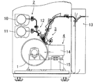
以下、この発明の実施の形態を図面に基づいて説明する。図1は校正装置の側面方向断面図である。図1において、校正装置は、感光材料をその周面に保持可能なドラム1と、このドラムに対し感光材料を供給および排出する供給手段2および排出手段3と、ドラム1上の感光材料に対しカラー画像を記録する記録手段4と、上記各部を制御するとともに画像データを処理するための制御手段(図2の5)とからなる。
【0027】
ドラム1は、その周面にシート状の感光材料を保持可能な円筒状部材であり、図示しない駆動モータにより回転可能に構成されている。供給手段2は、幅サイズの異なる2種のロール状感光材料を備えたカセット10、11と、各々のカセット10、11から引き出した感光材料をシート状に切断し、ドラム1まで搬送するシート搬送手段12とからなる。ここで感光材料はYMCに対応する3層の発色層を備える感光材料である。排出手段3は、ドラム1から記録済みの感光材料を剥離して後段の現像装置(図示しない)へ排出するものである。本実施の形態における排出手段3では、感光材料は記録面が下向きになって排出されるため、現像装置へ送り込む前に感光材料の表裏を反転する反転手段13が備えられている。記録手段4は、RGBの3波長の光源を備えたカラー画像を記録するための記録ヘッド14と、この記録ヘッド14をドラム1の軸線方向に沿って駆動するための送り手段15とからなる。なお、以後の説明では、前記ドラム1の回転方向を主走査方向、記録ヘッド14の移動方向を副走査方向とする。
【0028】
制御手段5は、CPUおよびメモリ、CRTなどの表示手段、マウスやキーボードなどの入力手段、およびハードディスクなどの記憶手段やバッファメモリなどを備えたコンピュータシステムであって、この実施の形態では、校正装置自体の制御と画像データの処理とを行うようにプログラムされている。
【0029】
この制御手段5の画像機能に係る構成については、図2のブロック図を用いて説明する。図において制御手段5は、前段の図示しないDTP(desk-top-publishing)装置などにより作成された画像データD0をRIP処理(Raster-Image-Processing)するためのRIP処理手段20と、処理された2値画像データD1を記憶するための記憶手段21と、記憶された2値画像データD1からK版の画像データに抜け画素を形成するための抜け画素変換手段22と、前記抜け画素変換手段22で変換した画像データD2をRGB変換するためのRGB変換手段23と、RGB変換手段23で生成した2値画像データD3を一時貯留するためのデータバッファ24と、データバッファ24に格納した2値画像データD3に基づいて前記記録ヘッド14を駆動するドライバー25とからなる。
【0030】
RIP処理手段20は、画像データをYMCKの各色版毎にビットマップ形式で表された2値画像データD1に変換するものである。このRIP処理後の2値画像データD1は各色版毎の画像データとして送出される。なお、この実施の形態では、校正装置側においてRIP処理するようにしているが、前段の画像データ作成装置などで処理してもよい。記憶手段21は、前記色版毎の2値画像データD1を4色分記憶可能な記憶容量を有したハードディスク装置などからなる。なお記憶手段21は、画像データを圧縮して記憶し、展開して読み出す圧縮展開手段を備えるものであってもよい。
【0031】
抜け画素変換手段22は、K版確認モードにおいてK版の画像データに対し抜け画素を形成するものである。この詳細については図3を用いて後述する。なお、通常のモードであればK版の画像データはそのまま何も変換を行わない。RGB変換手段23は、前記YMCKの各色版の画像データを記録ヘッド14の3波長光源に合わせてRGB変換してRGB画像データD3を生成するものである。なおRGB変換については公知の技術であり、YMCKの所定色の画像データの組み合わせにより対応するRGB色の画像データを生成するものであって、例えば特公平7−22346号などに記載されているため、ここでの説明は省略する。
【0032】
データバッファ24は、前記RGB変換された2値画像データD3を所定のブロック毎にバッファリングするためのメモリ装置であり、本実施の形態では主走査128ライン毎の画像データD3がRGB変換手段23からデータバッファ24に送出されてバッファリングされる。次の ドライバー25は前記データバッファに貯えられた画像データD3に基づき前記記録ヘッド14内の各光源をon/off制御する手段であり、これによってドラム1上の感光材料に対し画像を記録することができる。
【0033】
上述したように、前記制御手段5はマイクロコンピュータを備えたシステムであるが、各手段を各々別のコンピュータシステムにより構成するようにしてもよい。なお制御手段5は上記画像処理以外にも校正装置の各部の制御処理や後段の現像装置との通信制御処理なども行うが、ここでは説明を省略する。
【0034】
なお、上記実施の形態では、RGB変換手段23の後段にデータバッファ24を配置したが、この順序を逆にしてもよい。すなわち、まずデータバッファ24により適宜のブロックサイズの2値画像データD2(またはD1)を読み出し、それに応じてRGB変換手段23で順次画像データをRGB変換するようにしてもよい。
【0035】
次に本発明に係る抜け画素変換手段22の構成について図3の機能的ブロック図を用いて説明する。まず前記抜け画素変換手段22は、所定のアドレス長を有するラインメモリからなる配列メモリ30と、前記配列メモリ30に対しビット情報を書き込むための抜け画素位置設定手段31とを有する。前記配列メモリ30は、例えば図6(D)に示すようなラインメモリであって、各アドレスには「0」または「1」のビット情報が書き込まれる。また前記ラインメモリのアドレス長は、記録する最大画像データの主走査方向長と同じか、それよりも小さく設定されている。
【0036】
前記抜け画素位置設定手段31は、前記配列メモリ30の各アドレス上に、「0」または「1」のビット情報を設定するものである。例えば、前述したK版画像データ上に形成する抜け画素の割合を主走査方向および副走査方向に各々1/4とすると、この抜け画素位置設定手段31は前記配列メモリ30の4アドレス毎に「1」のビット情報を設定するものである。なお、前記抜け画素の割合は作業者が予め複数の数値から選択することができるものである。また主走査方向および副走査方向の割合は、画像処理の均一性から考えて同一が好ましいが、異なる割合を設定してもよい。
【0037】
また、抜け画素変換手段22は、前記YMCKの各2値画像データD1を記憶手段21から送出する画像データ送出手段32と、送出された画像データD1に基づいて画素の重なりを判断する判断手段33と、前記判断結果に基づき前記配列メモリ30からビット情報を読み出して変換指令信号を発生する配列メモリ読出手段34と、前記変換指令信号に基づいてK版の画像データの画素を抜け画素に変換する画素変換手段35とを有する。
【0038】
画像データ送出手段32は、前記抜け画素位置設定手段31で設定された抜け画素の割合に応じて抜け画素変換処理する主走査ラインを副走査方向にスキップするものである。例えば、前述のように抜け画素の割合が主走査方向および副走査方向とも1/4の場合、図6(B)で示すように副走査方向では4主走査ライン間隔で抜け画素変換を行なえばよい。すなわち変換を行う主走査ライン間の3本の主走査ラインでは抜け画素画素変換が不要なため、変換を行わずそのままK版の画像データを図のア方向で示すようにデータバッファ24へ送出する。一方、変換を行う主走査ラインの場合は、画像データ送出手段32がYMCKの各画像データD1を判断手段33に送出するとともに、K版の画像データを図のイ方向で示すように画素変換手段35へ送出する。なお、上記いずれであってもYMCの画像データは変換されずに図のア方向で示すようにデータバッファ24へ送出される。
【0039】
このようなスキップ動作は、例えば、画像データ送出手段32内に図示しないカウンターを備えておいて、主走査ラインの処理毎に当該カウンターを計数し、計数値が前記割合に達する毎に前記抜け画素変換を行なうよう画像データを送出すればよい。もしくは抜け画素位置設定手段31などが、前記割合に応じたタイミングでスキップを指令するようにしてもよい。なお通常モードのように抜け画素変換が全くない場合は、前記抜け画素位置設定手段31が前記画像データ送出手段32に対し、YMCKの全画像データを抜け画素変換せずに図のア方向で示すようにデータバッファ24へ送出するように指令する。
【0040】
この実施の形態のようなスキップ処理を行えば、画像データの変換に係る時間を短縮することができるという利点がある。しかしながら全ての場合において全画像データを判断手段33へ送出し、抜け画素変換を行わない主走査ラインでは判断手段33の判断結果を常に「画素の重なりがない」とすることで、同一処理ルーチンで処理するようにしてもよい。
【0041】
判断手段33では、YMCKの画像データD1に基づいてK版の画素とYMCの画素とが重なるかどうかを判断する。この判断は主走査方向に順次1画素づつ行われる。K版の画素値が「1」であり、かつYMCのいずれかの画素値が「1」の場合には重なりがあると判断して、配列メモリ読出手段34に読出指令信号を出力する。一方、重なりがないと判断された場合は前記画素変換手段35へ変換不要信号を出力する。
【0042】
配列メモリ読出手段34は、判断手段33からの読出指令信号に応じて前記配列メモリ30のビット情報を読み出すものであって、「1」のビット情報を読み出した場合は変換指令信号を画素変換手段35に出力し、「0」のビット情報を読み出した場合は変換不要信号を画素変換手段35へ出力する。なお、この読み出しは順次配列メモリ30のアドレスが順次インクリメントされて行われ、読み出しが最終アドレスに至った場合は開始アドレスにサイクリックに復帰するようにしている。これにより配列メモリ30のアドレス長を主走査ライン長よりも短く設定することができる。なお当然のことながら配列メモリ30のアドレス長が主走査ライン長以上であれば、上記のようなサイクリックな使用をしなくてもよい。
【0043】
画素変換手段35は、前記変換不要信号または変換指令信号の入力にともないK版の画像データを各画素毎に処理するものであって、変換指令信号が入力された場合は画素値を「1」から「0」に変換し、変換不要信号が入力された場合は画素値を変換しない。
【0044】
この抜け画素変換手段22では、前記配列メモリ30に設定されたビット情報に基づいて抜け画素を設定することができる。なお上記の例では前記配列メモリ30に設定されたビット情報は、一定画素間隔に配置されているが、設定された割合に応じてランダムな配置にしてもよい。例えば、抜け画素の一定配列によりモアレパターンなどが生じる可能性があるときに有効である。また前記配列メモリ30の読み出し開始アドレスを各主走査ライン毎に適宜オフセット変更してもよい。
【0045】
次に前記校正装置における動作について図4および図5のフローチャートを用いて説明する。なお図4は校正出力を行う全体作業のフローを示すフローチャートであり、図5は前記抜け画素変換に伴う画像データ変換のフローを示すフローチャートである。まずステップS1では、校正作業を行うにあたっての初期設定が行われる。この初期設定では、K版を通常どおり出力する通常モードとK版の重なり状態を確認する確認モードとの出力モードの切替設定や、前記確認モードにおける抜け画素の割合を設定することができる。また、他の設定として、印刷する画像データの選定や出力枚数や出力サイズなどの設定も行なわれる。
【0046】
ステップS2では感光材料がドラム1に対し供給される。すなわち前記カセットマガジン10または11から出力サイズに応じて感光材料が切り出されてドラム1に巻回される。ステップS3では前記出力モードが確認され、通常モードの場合はステップS4に進み通常の画像データ変換が行われる。すなわち画像データD0がRIP処理されてYMCKの2値の画像データD1に変換され、ついでRGB変換によって画像データD3に変換される。確認モードの場合はステップS3からステップS5へ進み、抜け画素変換を含む画像データ変換が行われる。すなわち画像データD0がRIP処理されてYMCKの2値の画像データD1に変換され、ついで抜け画素変換により画像データD2に変換され、最後にRGB変換によって画像データD3に変換される。
【0047】
ステップS6では、前記ステップS4またはS5により変換された画像データに基づいて露光が行われる。そして露光が終了すれば、ステップS7で感光材料がドラム1より排出され、ついでステップS8では後段の現像処理装置によって現像処理される。
【0048】
上記フローでは理解しやすいように各工程を直列に示しているが、可能であれば各工程を並行に処理したり所定の工程を前後させてもよい。一例として、例えばステップS2の感光材料の供給に先駆けて画像データの変換を行ってもよい。また画像データの変換を行いつつ順次変換が終了した画像データにより並行して露光を行っても良い。
【0049】
続いて、前記ステップS5における画像データ変換の中から抜け画素変換の工程だけを説明する。まずステップP1では配列メモリ30が準備される。すなわち設定された抜け画素の割合に応じて前記配列メモリ30上に抜け画素を設定するタイミングを表すビット情報「1」を書き込む。ステップP2からは、該当する主走査方向に順次K色の画素とYMCの画素との重なりを判断する。ここで該当する画素に重なりがあった場合はステップP3へ進み、ない場合は該当するK版の画素の変換を行わずにステップP6へ進む。
【0050】
ステップP3では、前記配列メモリ30を順次読み出す。そしてステップP4では読み出したビット情報が「1」であれば抜け画素変換位置であると判断してステップP5へ進み、「0」であれば該当するK版の画素の変換を行わずにステップP6へ進む。ステップP5では該当するK版の画素を「1」から「0」に変換して抜け画素を形成する。ステップP6では該当する主走査ライン上の全ての画素に対し処理が終了したかどうかを判断し、処理が終了した場合はステップP7へ進み、処理が終了していない場合はステップP8で処理を行う画素のアドレスを次画素にインクリメントしてステップP2へ戻る。
【0051】
該当する主走査ラインにおける変換が終了すれば、ステップP7では前記割合に応じて主走査ラインがスキップされる。そしてステップP9では全主走査ラインに対し処理が終了したかどうかを判断する。全てのラインが終了したと判断されれば本フローは終了する。まだ処理されていない主走査ラインが残存する場合は、主走査方向の画素アドレスや配列メモリの読み出しアドレスなどをリセットしてステップP2へ戻る。
【0052】
[その他の実施の形態]
(1)前記配列メモリ30に設定するビット情報とK版の画像データの画素値とを論理演算して抜け画素変換を行うようにしてもよい。例えば前記配列メモリ30に設定するビット情報を、抜け画素の有る場合に「0」、ない場合に「1」と設定し、前記配列メモリ読出手段34で読み出したビット情報とK版の画像データの画素値との論理積をとればよい。
【0053】
(2)前記配列メモリ30のアドレスは、K版の画素が重なった場合に順次インクリメントされるよう構成されているが、各画素を判断する毎にインクリメントされるように構成しても巨視的には同一の効果がある。
【0054】
(3)前記配列メモリ30にはライン状のアドレス設定をしたメモリを用いたが、2次元のアドレス設定をしたメモリを用いてもよい。また配列メモリ30を用いずに、所定のカウンタを用いて抜け画素を設定する間隔を計数するようにしてもよい。例えば、K版の画素が他版の画素と重なる回数をカウンターにより計数し、所定の回数毎に抜け画素に変更する構成などが考えられる。
【0055】
【発明の効果】
請求項1に記載の発明では、K版の画素と他の色版の画素とが重なる場合に適宜の割合でK版の画素を抜け画素に変更するため、作業者が目視した場合にK版を透かしたように他色の画像を視認することができる。これによりトラップ処理や文字のせなどの製版作業を確認することができる。
【0056】
請求項2に記載の発明では、定められた一定の画素間隔で抜け画素への変換を行うことができるため、変換作業を簡易にすることができる。
【0057】
請求項3に記載の発明は、画素間隔を可変することができるので、K版に重なる他の色版の透過の具合を可変することができる。
【0058】
請求項4に記載の発明では、副走査方向に所定数の主走査ラインをスキップするようにしているので、画像変換工程を短縮することができる。
【0059】
請求項5に記載の発明は、ラインメモリに抜け画素位置を設定する用にしているので、種々の抜け画素配置パターンを容易に設定することができる。
【0060】
請求項6に記載の発明は、ラインメモリをサイクリックに使用することで小さなラインメモリを使用することができる。
【0061】
請求項7に記載の発明は、主走査方向の抜け画素位置を適宜変更することにより、簡単な手法で抜け画素の配置パターンが均一になることを防止することができる。
【0062】
請求項8に記載の発明は、抜け画素の配置を乱数設定することによりモアレパターンの発生の可能性を少なくすることができる。
【0063】
請求項9に記載の発明は、抜け画素の配置を設定するラインメモリを備えなくてもよいという効果がある。
【0064】
請求項10に記載の発明は、K版の重ね状態を観察可能な第1のモードと通常の第2のモードとを切替可能としているので、例えば製版作業の確認が主であれば第1のモード、色具合などを確認するのが主であれば第2のモードというように目的にあって切り替えることができる。
【0065】
請求項11および12に記載の発明では、K版の画素と他の色版の画素とが重なる場合に適宜の割合でK版の画素を抜け画素に変更するため、作業者が目視した場合にK版を透かしたように他色の画像を視認することができる。これによりトラップ処理や文字のせなどの製版作業を確認することができる。特にYMC上に重ねられたK色の重ね状態が判別しにくい3層の発色層を備える感光材料では効果が大きい。
【0066】
請求項13に記載の発明では、定められた一定の画素間隔で抜け画素への変換を行うことができるため、変換作業を簡易にすることができる。
【0067】
請求項14に記載の発明では、副走査方向に所定数の主走査ラインをスキップするようにしているので、画像変換工程を短縮することができる。
【0068】
請求項15に記載の発明は、抜け画素の配置を乱数設定することによりモアレパターンの発生の可能性を少なくすることができる。
【図面の簡単な説明】
【図1】この発明の実施の形態における校正装置の側面概要図である。
【図2】同校正装置において画像データ処理関係の制御を行う制御手段のブロック図である。
【図3】同制御手段における抜け画素変換手段の機能的なブロック図である。
【図4】同校正装置の作業工程を表すフローチャートである。
【図5】抜け画素変換の工程を表すフローチャートである。
【図6】抜け画素に係る説明図である。
【符号の説明】
1 ドラム
2 供給手段
3 排出手段
4 記録手段
5 制御手段
14 記憶ヘッド
22 抜け画素変換手段
30 配列メモリ
31 抜け画素位置設定手段
32 画像データ送出手段
33 判断手段
34 配列メモリ読出手段
35 画素変換手段[0001]
[Industrial application fields]
The present invention relates to a calibration apparatus and a calibration method for performing calibration printing by recording on a photosensitive material based on image data obtained by laying out images and characters constituting a printed matter.
[0002]
[Prior art]
In the conventional process for producing printed matter, there is a calibration work for inspecting and correcting whether or not the plate-making is finished as instructed, and several proofreading work is done before the final printed matter is finished. Various proofing apparatuses for creating color prints for proofing for this proofing work are known. For example, digital image data color-separated into Y (yellow) M (magenta) C (cyan) K (black) is used. There is a calibration device for recording an image on a photosensitive material.
[0003]
As one of such proofing apparatuses, there is an apparatus for recording an image with a three-wavelength laser light source or the like on a photosensitive material provided with three color developing layers corresponding to each color plate of YMC. In the light-sensitive material having such three light emitting layers, KMC (black) color is developed by performing YMC three-color unexposed (in the case of positive) or YMC three-color full exposure (in the case of negative). Have achieved.
[0004]
By the way, in the above-described proof printing, it is preferable to faithfully reproduce the proof image in conformity with the main printing in order to confirm the color condition of the printed material. Also used to confirm. As one example of plate making work, there is a case where “trap processing” or “overlay processing” is performed in anticipation of misregistration of printed matter. This is because a part of the image is previously covered with the other image so that a gap is not exposed between the images even if there is a misregistration in the accurate joining of two or more images as referred to as “tweeping”. For example, a process or a process of placing a character image on another image as referred to as “character overlay” or the like. In the calibration work, it is preferable to be able to confirm whether or not such “trap processing” and “overlay processing” are accurately performed.
[0005]
[Problems to be solved by the invention]
In the “trap processing” and “overlay processing” as described above, images are superimposed on the printed matter. Here, in the case of a general offset printing machine or offset proofing machine, for example, the color of the area where the K color image overlaps the image of the other color and the color of the area of only the K color are the same black. Also slightly different color development. As a result, a skilled worker can also confirm the “trap process” and “placement process” as described above.
[0006]
However, when the photosensitive material having the three color-developing layers corresponding to YMC as described above is used, the K color is expressed by the unexposed or full exposure of the YMC three colors. The same color was generated in the region where the colors overlapped, and it was not possible to confirm “trap processing” or “overlay processing” using the K color. For this reason, even if the instructed plate making process is unprocessed, there is a possibility of being overlooked.
[0007]
The present invention has been made to solve the above-described problem, and an object of the present invention is to provide a calibration method and a calibration apparatus that can easily check a region in which the K color overlaps with other colors, and particularly corresponds to YMC. An object of the present invention is to provide a calibration apparatus and a calibration method that are optimum when a photosensitive material having three color-developing layers is used.
[0008]
[Means for Solving the Problems]
The invention according to
[0009]
According to a second aspect of the present invention, in the calibration apparatus according to the first aspect, the pixel conversion is performed at a pixel interval determined along the main scanning direction.
[0010]
According to a third aspect of the present invention, in the calibration apparatus according to the second aspect, the pixel interval can be selected from a predetermined value.
[0011]
According to a fourth aspect of the present invention, in the calibration apparatus according to the second or third aspect, the determination unit performs the determination for each main scanning line having a substantially same interval as the pixel interval in the sub-scanning direction. It is characterized by having done.
[0012]
According to a fifth aspect of the present invention, in the calibration device according to any one of the first to fourth aspects, the missing pixel conversion means corresponds to a line memory having a predetermined address length and each address of the line memory. A missing pixel position setting means capable of setting the position of a missing pixel, and a line memory reading means for reading out values in the line memory in order of addresses in synchronization with a timing determined by the determination means. According to the present invention, the K-version pixel is subjected to pixel conversion in accordance with the value read by the reading means.
[0013]
According to a sixth aspect of the present invention, in the calibration apparatus according to the fifth aspect, the line memory reading means cyclically reads the line memory.
[0014]
According to a seventh aspect of the present invention, in the calibration apparatus according to the fifth or sixth aspect, the line memory reading unit changes a read start address for each corresponding main scanning line.
[0015]
According to an eighth aspect of the present invention, in the calibration apparatus according to the first aspect, the missing pixel position setting means arranges the missing position by a random number.
[0016]
According to a ninth aspect of the present invention, in the calibration apparatus according to any one of the first to third aspects, the number of times that the missing pixel converting unit determines that the K plane pixel overlaps with the other plane pixel by the determining unit. And every time the count reaches a predetermined value, the corresponding K plate pixel is converted into a missing pixel.
[0017]
The invention according to
[0018]
The invention according to
[0019]
According to a twelfth aspect of the present invention, in the calibrating method according to the eleventh aspect, the calibrating apparatus exposes a photosensitive material having three color developing layers corresponding to three colors of YMC, The color is expressed by YMC three-color unexposed or three-color full exposure.
[0020]
According to a thirteenth aspect of the present invention, in the calibration method according to the eleventh or twelfth aspect, the missing pixel conversion step performs pixel conversion at predetermined pixel intervals that are selectively determined in advance. Features.
[0021]
According to a fourteenth aspect of the present invention, in the calibration method according to the thirteenth aspect, the missing pixel conversion step performs pixel conversion at regular pixel intervals along the main scanning direction, and in the sub scanning direction. The determination step is performed with an interval substantially the same as the pixel interval.
[0022]
The invention according to
[0023]
DETAILED DESCRIPTION OF THE INVENTION
[Principle of the present invention]
First, the principle of confirming the overlapping state of the K plate and other color plates in the present invention will be described. In the following description, an example in which a positive photosensitive material having three color developing layers corresponding to YMC is used as a photosensitive material for forming an image will be described. Each image is formed of a binary image. FIG. 6A is a diagram showing an example in which the K version letter “E” is placed on a halftone area m composed of 50% halftone dots of the M version. In the conventional example, the left half of the letter “E” on the halftone area m and the right half of the letter “E” on the paper white area h (an area where there is no other color image) are the same K color. It becomes.
[0024]
On the other hand, in the present invention, as shown in FIG. 6B, in the place where the halftone dot on the halftone area m exists, the K plate image is missing every four pixels to form a pixel. That is, the K version image has no pixel at an interval of 4 pixels (pixel value is 0, hereinafter referred to as “missing pixel”), and the overlapped M version pixels can be visually recognized in that portion. In the calibration apparatus according to this embodiment, the one pixel has a size of about 10 μm with a resolution of 2400 dpi. Accordingly, as shown in FIG. 6C, the M plate is visible through the human eye as if it were the base.
[0025]
As described above, in the proofreading apparatus of the present invention, when the K plate pixel overlaps with the other color plate pixels, the other color plate overlapped with the K plate is obtained by replacing the K plate pixels at a predetermined ratio. Can be visually recognized. Hereinafter, the normal mode is output as in FIG. 6A, and the mode in which missing pixels are formed on the K plate and the overlapping state of the K plate can be confirmed as shown in FIG. 6C is confirmed. This is called a mode.
[0026]
[Embodiment of calibration apparatus]
Hereinafter, embodiments of the present invention will be described with reference to the drawings. FIG. 1 is a side sectional view of the calibration apparatus. In FIG. 1, the calibration apparatus includes a
[0027]
The
[0028]
The control means 5 is a computer system including a CPU and memory, display means such as a CRT, input means such as a mouse and keyboard, storage means such as a hard disk, buffer memory, etc. In this embodiment, the calibration device It is programmed to perform its own control and image data processing.
[0029]
The configuration related to the image function of the control means 5 will be described with reference to the block diagram of FIG. In the figure, the control means 5 is processed with the RIP processing means 20 for performing RIP processing (Raster-Image-Processing) on the image data D0 created by a DTP (desk-top-publishing) device (not shown) in the previous stage. Storage means 21 for storing binary image data D1, missing pixel conversion means 22 for forming missing pixels from the stored binary image data D1 into K-plane image data, and missing pixel conversion means 22 RGB conversion means 23 for performing RGB conversion on the image data D2 converted in
[0030]
The RIP processing means 20 converts the image data into binary image data D1 represented in a bitmap format for each color plate of YMCK. The binary image data D1 after the RIP process is sent out as image data for each color plate. In this embodiment, the RIP processing is performed on the calibration device side, but the processing may be performed by the preceding image data creation device or the like. The storage means 21 includes a hard disk device having a storage capacity capable of storing the binary image data D1 for each color plate for four colors. The
[0031]
The missing pixel conversion means 22 forms missing pixels for the K plane image data in the K plane confirmation mode. Details of this will be described later with reference to FIG. In the normal mode, no conversion is performed on the K version image data. The RGB conversion means 23 generates RGB image data D3 by subjecting the YMCK color image data to RGB conversion in accordance with the three-wavelength light source of the
[0032]
The
[0033]
As described above, the control means 5 is a system including a microcomputer, but each means may be configured by a separate computer system. In addition to the image processing described above, the control means 5 also performs control processing for each part of the proofing device, communication control processing with the subsequent developing device, and the like, but the description thereof is omitted here.
[0034]
In the above embodiment, the
[0035]
Next, the configuration of the missing pixel conversion means 22 according to the present invention will be described with reference to the functional block diagram of FIG. First, the missing pixel conversion means 22 includes an
[0036]
The missing pixel position setting means 31 sets bit information “0” or “1” on each address of the
[0037]
Further, the missing
[0038]
The image data sending means 32 skips the main scanning line for missing pixel conversion processing in the sub-scanning direction according to the ratio of missing pixels set by the missing pixel position setting means 31. For example, when the ratio of missing pixels is 1/4 in both the main scanning direction and the sub-scanning direction as described above, missing pixel conversion is performed at intervals of four main scanning lines in the sub-scanning direction as shown in FIG. Good. That is, missing pixel conversion is not necessary for the three main scanning lines between the main scanning lines to be converted, and therefore K image data is sent as it is to the
[0039]
Such a skip operation includes, for example, a counter (not shown) in the image data sending means 32, counts the counter every time the main scanning line is processed, and the missing pixel every time the count value reaches the ratio. What is necessary is just to send image data for conversion. Alternatively, the missing pixel
[0040]
If the skip processing as in this embodiment is performed, there is an advantage that the time required for the conversion of the image data can be shortened. However, in all cases, all the image data is sent to the
[0041]
The
[0042]
The array memory reading means 34 reads the bit information of the
[0043]
The pixel conversion means 35 processes the K version image data for each pixel in response to the input of the conversion unnecessary signal or the conversion command signal. When the conversion command signal is input, the pixel value is set to “1”. Is converted from “0” to “0”, and when a conversion unnecessary signal is input, the pixel value is not converted.
[0044]
In the missing pixel conversion means 22, missing pixels can be set based on the bit information set in the
[0045]
Next, the operation of the calibration apparatus will be described with reference to the flowcharts of FIGS. FIG. 4 is a flowchart showing the overall work flow for performing calibration output, and FIG. 5 is a flowchart showing the flow of image data conversion accompanying the missing pixel conversion. First, in step S1, an initial setting for performing calibration work is performed. In this initial setting, it is possible to set the output mode switching between the normal mode for outputting the K plate as usual and the confirmation mode for confirming the overlapping state of the K plate, and the ratio of missing pixels in the confirmation mode. In addition, as other settings, selection of image data to be printed, setting of the number of output sheets, output size, and the like are also performed.
[0046]
In step S <b> 2, a photosensitive material is supplied to the
[0047]
In step S6, exposure is performed based on the image data converted in step S4 or S5. When the exposure is completed, the photosensitive material is discharged from the
[0048]
In the above flow, each process is shown in series for easy understanding, but if possible, each process may be processed in parallel or a predetermined process may be moved back and forth. For example, the image data may be converted prior to the supply of the photosensitive material in step S2. Further, the image data may be converted and the exposure may be performed in parallel with the image data that has been sequentially converted.
[0049]
Subsequently, only the process of missing pixel conversion from the image data conversion in step S5 will be described. First, at step P1, the
[0050]
In step P3, the
[0051]
When the conversion in the corresponding main scanning line is completed, the main scanning line is skipped in step P7 according to the ratio. In step P9, it is determined whether or not processing has been completed for all main scanning lines. If it is determined that all lines have been completed, this flow ends. If a main scanning line that has not yet been processed remains, the pixel address in the main scanning direction, the read address of the array memory, and the like are reset, and the process returns to step P2.
[0052]
[Other embodiments]
(1) The missing pixel conversion may be performed by performing a logical operation on the bit information set in the
[0053]
(2) The address of the
[0054]
(3) As the
[0055]
【The invention's effect】
According to the first aspect of the present invention, when the K plate pixel and another color plate pixel overlap, the K plate pixel is changed to a missing pixel at an appropriate ratio. It is possible to visually recognize an image of another color as if it is watermarked. As a result, it is possible to confirm plate making operations such as trap processing and letter placement.
[0056]
According to the second aspect of the present invention, since conversion to missing pixels can be performed at a predetermined fixed pixel interval, conversion work can be simplified.
[0057]
According to the third aspect of the present invention, since the pixel interval can be changed, the degree of transmission of other color plates overlapping the K plate can be changed.
[0058]
In the fourth aspect of the invention, since a predetermined number of main scanning lines are skipped in the sub-scanning direction, the image conversion process can be shortened.
[0059]
Since the invention according to
[0060]
The invention according to claim 6 can use a small line memory by cyclically using the line memory.
[0061]
According to the seventh aspect of the present invention, it is possible to prevent the missing pixel arrangement pattern from becoming uniform by a simple method by appropriately changing the missing pixel position in the main scanning direction.
[0062]
According to the eighth aspect of the present invention, the possibility of the occurrence of a moire pattern can be reduced by setting the arrangement of missing pixels as a random number.
[0063]
According to the ninth aspect of the invention, there is an effect that it is not necessary to provide a line memory for setting the arrangement of missing pixels.
[0064]
In the invention according to
[0065]
In the inventions according to
[0066]
In the invention according to the thirteenth aspect, conversion to missing pixels can be performed at a predetermined fixed pixel interval, so that the conversion work can be simplified.
[0067]
In the invention described in
[0068]
According to the fifteenth aspect of the present invention, it is possible to reduce the possibility of the occurrence of a moire pattern by setting a random pixel layout.
[Brief description of the drawings]
FIG. 1 is a schematic side view of a calibration device according to an embodiment of the present invention.
FIG. 2 is a block diagram of a control unit that controls image data processing in the calibration apparatus.
FIG. 3 is a functional block diagram of missing pixel conversion means in the control means.
FIG. 4 is a flowchart showing an operation process of the calibration apparatus.
FIG. 5 is a flowchart showing a missing pixel conversion process.
FIG. 6 is an explanatory diagram relating to missing pixels.
[Explanation of symbols]
1 drum
2 Supply means
3 Discharge means
4 Recording means
5 Control means
14 Memory head
22 missing pixel conversion means
30 array memory
31. Missing pixel position setting means
32 Image data sending means
33 Judgment means
34 Array memory reading means
35 pixel conversion means
Claims (15)
所定のRIP処理手段によって一の画像データを2値化することにより得られる画像データの間において、K版の画像データと他の色版の画像データとを画素毎に比較して、K版の画素が他の色版のいずれかの画素と重なるかどうかを判断する判断手段と、
前記判断手段において重なると判断された場合に前記K版の画素を所定の割合で画素値が0である抜け画素になるように画素変換する抜け画素変換手段と、を備える校正装置。A proofing device that obtains proof printing by performing exposure for each color on a photosensitive material having at least three color developing layers corresponding to each color plate of YMC,
Between the image data obtained by binarizing one image data by a predetermined RIP processing means, the K plate image data and the other color plate image data are compared for each pixel, and the K plate A judging means for judging whether or not the pixel overlaps any pixel of another color plate;
A calibration apparatus comprising: missing pixel conversion means for performing pixel conversion so that the pixels of the K plate become missing pixels having a pixel value of 0 at a predetermined ratio when it is determined by the determination means to overlap.
所定のアドレス長を有するラインメモリと、
前記ラインメモリの各アドレスに対応して抜け画素の位置を設定可能な抜け画素位置設定手段と、
前記判断手段が判断するタイミングに同期して、前記ラインメモリ内の値をアドレス順に読み出すラインメモリ読出手段と、を備え、
前記ラインメモリ読出手段で読み出した値に応じて前記K版の画素を画素変換することを特徴とする請求項1ないし4のいずれかに記載の校正装置。The missing pixel conversion means includes
A line memory having a predetermined address length;
A missing pixel position setting means capable of setting a position of a missing pixel corresponding to each address of the line memory;
Line memory reading means for reading values in the line memory in the order of addresses in synchronization with the timing determined by the determining means,
5. The calibration apparatus according to claim 1, wherein the K-version pixel is subjected to pixel conversion in accordance with a value read by the line memory reading means.
所定のRIP処理手段によって一の画像データを2値化することにより得られる画像データの間において、K版の画像データと他の色版の画像データとを画素毎に比較してK版の画素が他の色版のいずれかの画素と重なるかどうかを判断するとともに、重なると判断された場合には前記K版の画素を所定の割合で画素値が0である抜け画素になるように画素変換する第1のモードと、
前記判断を行わず、K版の画像データに対し前記画素変換を行わない第2のモードとを備え、いずれかのモードを選択的に実行可能な校正装置。A proofing device that performs color proofing printing based on image data,
Between the image data obtained by binarizing one image data by a predetermined RIP processing means, the K plate image data and the other color plate image data are compared for each pixel and the K plate pixel Is determined to overlap with any other pixel of the other color plate, and if it is determined to overlap, the pixel of the K plate is a missing pixel having a pixel value of 0 at a predetermined ratio. A first mode to convert;
And a second mode in which the pixel conversion is not performed on the K-plane image data without performing the determination, and a calibration apparatus capable of selectively executing any mode.
所定のRIP処理手段によって一の画像データを2値化することにより各色版の画像データを準備する工程と、
前記各色版の間において、K版の画像データと他の色版の画像データとを画素毎に比較して、K版の画素が他の色版のいずれかの画素と重なるかどうかを判断する判断工程と、
前記判断工程において画素が重なると判断された場合は、前記K版の画素を所定の割合で画素値が0である抜け画素になるように画素変換する抜け画素変換工程と、からなる校正方法。A calibration method capable of confirming an overlapping state between a K plate and another color plate using a proofing device that performs color proof printing based on image data,
Preparing image data of each color plate by binarizing one image data by a predetermined RIP processing means ;
Between each of the color plates, the image data of the K plate and the image data of the other color plate are compared for each pixel to determine whether the K plate pixel overlaps any pixel of the other color plate. A decision process;
A calibration method comprising: a missing pixel conversion step of performing pixel conversion so that pixels of the K plate are converted to missing pixels having a pixel value of 0 at a predetermined ratio when it is determined that pixels overlap in the determination step.
Priority Applications (1)
| Application Number | Priority Date | Filing Date | Title |
|---|---|---|---|
| JP2000304319A JP3698979B2 (en) | 2000-10-04 | 2000-10-04 | Calibration apparatus and calibration method |
Applications Claiming Priority (1)
| Application Number | Priority Date | Filing Date | Title |
|---|---|---|---|
| JP2000304319A JP3698979B2 (en) | 2000-10-04 | 2000-10-04 | Calibration apparatus and calibration method |
Publications (2)
| Publication Number | Publication Date |
|---|---|
| JP2002103692A JP2002103692A (en) | 2002-04-09 |
| JP3698979B2 true JP3698979B2 (en) | 2005-09-21 |
Family
ID=18785383
Family Applications (1)
| Application Number | Title | Priority Date | Filing Date |
|---|---|---|---|
| JP2000304319A Expired - Lifetime JP3698979B2 (en) | 2000-10-04 | 2000-10-04 | Calibration apparatus and calibration method |
Country Status (1)
| Country | Link |
|---|---|
| JP (1) | JP3698979B2 (en) |
-
2000
- 2000-10-04 JP JP2000304319A patent/JP3698979B2/en not_active Expired - Lifetime
Also Published As
| Publication number | Publication date |
|---|---|
| JP2002103692A (en) | 2002-04-09 |
Similar Documents
| Publication | Publication Date | Title |
|---|---|---|
| US7058196B2 (en) | Apparatus and method for processing image and computer-readable storage medium | |
| US20100103435A1 (en) | Image processing apparatus and image processing method for processing screen-processed image | |
| JP2005354414A (en) | Image processing apparatus and method | |
| US8441690B2 (en) | Image processing apparatus and image processing method for processing screen-processed image | |
| JP3927948B2 (en) | Image forming apparatus control method and image forming apparatus | |
| JP3902907B2 (en) | Image processing apparatus and method, and image forming apparatus | |
| JP5441758B2 (en) | Printing apparatus, printing apparatus control method, and program | |
| JP3698979B2 (en) | Calibration apparatus and calibration method | |
| JP4115294B2 (en) | Image processing apparatus and method | |
| JP4147242B2 (en) | Image processing apparatus control method and image processing apparatus | |
| JP4454786B2 (en) | Image processing apparatus and control method thereof | |
| JP2004209989A5 (en) | ||
| JP3565251B2 (en) | Image forming device | |
| JP2714215B2 (en) | Output device | |
| JP3778265B2 (en) | Image processing method and image processing apparatus | |
| JP4204682B2 (en) | Image forming apparatus | |
| JP3728017B2 (en) | Color image forming apparatus and control method thereof | |
| JP3245291B2 (en) | Image forming apparatus and image forming method | |
| JP3775023B2 (en) | Image processing device | |
| JP3302039B2 (en) | Image processing device | |
| JP2008205611A (en) | Image processing circuit and printer controller equipped with the same | |
| JP2000333024A (en) | Color image recorder | |
| JP2002108595A (en) | Printing device | |
| JP2003230002A (en) | Image rotation processing method, image processing apparatus, and image forming device provided with the same | |
| JP2007036514A (en) | Image conversion system |
Legal Events
| Date | Code | Title | Description |
|---|---|---|---|
| RD03 | Notification of appointment of power of attorney |
Free format text: JAPANESE INTERMEDIATE CODE: A7423 Effective date: 20040210 |
|
| A131 | Notification of reasons for refusal |
Free format text: JAPANESE INTERMEDIATE CODE: A131 Effective date: 20040720 |
|
| A521 | Written amendment |
Free format text: JAPANESE INTERMEDIATE CODE: A523 Effective date: 20040819 |
|
| TRDD | Decision of grant or rejection written | ||
| A01 | Written decision to grant a patent or to grant a registration (utility model) |
Free format text: JAPANESE INTERMEDIATE CODE: A01 Effective date: 20050705 |
|
| A61 | First payment of annual fees (during grant procedure) |
Free format text: JAPANESE INTERMEDIATE CODE: A61 Effective date: 20050706 |
|
| R150 | Certificate of patent or registration of utility model |
Free format text: JAPANESE INTERMEDIATE CODE: R150 |
|
| FPAY | Renewal fee payment (event date is renewal date of database) |
Free format text: PAYMENT UNTIL: 20080715 Year of fee payment: 3 |
|
| FPAY | Renewal fee payment (event date is renewal date of database) |
Free format text: PAYMENT UNTIL: 20090715 Year of fee payment: 4 |
|
| FPAY | Renewal fee payment (event date is renewal date of database) |
Free format text: PAYMENT UNTIL: 20090715 Year of fee payment: 4 |
|
| FPAY | Renewal fee payment (event date is renewal date of database) |
Free format text: PAYMENT UNTIL: 20090715 Year of fee payment: 4 |
|
| FPAY | Renewal fee payment (event date is renewal date of database) |
Free format text: PAYMENT UNTIL: 20100715 Year of fee payment: 5 |
|
| FPAY | Renewal fee payment (event date is renewal date of database) |
Free format text: PAYMENT UNTIL: 20100715 Year of fee payment: 5 |
|
| FPAY | Renewal fee payment (event date is renewal date of database) |
Free format text: PAYMENT UNTIL: 20100715 Year of fee payment: 5 |