JP3697802B2 - Optical module - Google Patents
Optical module Download PDFInfo
- Publication number
- JP3697802B2 JP3697802B2 JP32392296A JP32392296A JP3697802B2 JP 3697802 B2 JP3697802 B2 JP 3697802B2 JP 32392296 A JP32392296 A JP 32392296A JP 32392296 A JP32392296 A JP 32392296A JP 3697802 B2 JP3697802 B2 JP 3697802B2
- Authority
- JP
- Japan
- Prior art keywords
- waveguide element
- optical fiber
- fixed
- optical module
- longitudinal direction
- Prior art date
- Legal status (The legal status is an assumption and is not a legal conclusion. Google has not performed a legal analysis and makes no representation as to the accuracy of the status listed.)
- Expired - Fee Related
Links
Images

Landscapes
- Optical Couplings Of Light Guides (AREA)
Description
【0001】
【発明の属する技術分野】
本発明は、光ファイバ通信に用いられる光モジュールに関する。
【0002】
【従来の技術】
光ファイバ通信に用いられる光部品の一つに光モジュールがある。
【0003】
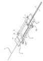
図4は光モジュールの従来例を示す外観斜視図である。
【0004】
光ファイバ1が導波路素子2に融着接続され、導波路素子2が非金属弾性体を介して台座3に固定されている。光ファイバ1は金属製のパッケージ4内に形成されたスロット5に樹脂で固定されている。パッケージ4の側面には長手方向に沿って素子固定用基準壁6が形成されている。導波路素子2はこの素子固定用基準壁6に押しあてられている。
【0005】
図5は光モジュールの他の従来例を示す外観斜視図である。
【0006】
同図に示すように光ファイバ1が導波路素子2に融着接続され、導波路素子2が非金属弾性体を介して台座3に固定されている。光ファイバ1はパッケージ4内に形成されたスロット5内に樹脂で固定されている。尚、融着部7から3〜5mmまでの光ファイバ1の被覆は除去されている。
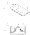
【0007】
図6は光モジュールの他の従来例を示す外観斜視図である。
【0008】
導波路アレイ部8を有する導波路素子2は丸みを帯びた長方形の台座3aに導波路アレイ部8ごと接着固定されている。
【0009】
【発明が解決しようとする課題】
ところで図4に示した光モジュールは、導波路素子2の長手方向の位置に対する基準がないため、目視により導波路素子2をパッケージ4の中心になるように位置合わせを行った後固定していた。そのため導波路素子2を固定した後、導波路素子2の位置を測定すると、固定位置の許容範囲からはみ出ていることがあった。
【0010】
また、図5に示した光モジュールは、光ファイバ1を固定するスロット5が0.5mm以下と細く、機械加工によりパッケージ4に形成されるため、目に見えない金属のバリが残っており、実装中にそのバリが飛散し、被覆が除去された光ファイバ1に傷が付いたり、プルーフ試験で光ファイバ1が破断してしまうことがあった。また、導波路素子2には目視では確認できないほど小さいカケ等の脆い部分が製造工程で発生することがある。外部からの衝撃や振動によりこれらの脆い部分からガラスが飛散して光ファイバ1に傷を付けることがあり、長期信頼性の保証が困難である。
【0011】
さらに図6に示した光モジュールは、導波路アレイ部8まで台座3aに固定されるが、導波路アレイ部8は応力に敏感であるため、導波路素子2の光学特性が固定前と比較すると変化する。特に中心波長が最大0.32nm(平均0.05nm)も移動することがある。
【0012】
そこで、本発明の目的は、上記課題を解決し、信頼性の高い光モジュールを提供することにある。
【0013】
【課題を解決するための手段】
上記目的を達成するために本発明は、金属パッケージと、該金属パッケージ上に形成された台座と、該台座に非金属弾性体を介して固定された導波路素子と、該導波路素子に固定された光ファイバとを備え、該光ファイバが上記金属パッケージの長手方向に形成されたスロットに固定されている光モジュールであって、
上記金属パッケージは、該金属パッケージの側面に長手方向に沿って形成された素子固定用基準壁と、上記導波路素子の長手方向の前後であり、かつ上記スロットから離間した位置に設けられ上記導波路素子の長手方向の移動を規制する凸状のストッパとを備えたものである。
【0014】
上記構成に加え本発明は、ストッパの間隔が、導波路素子の長手方向の長さ以上であり、導波路素子の長さに2mmを加えた値以下であるのが好ましい。
【0019】
本発明によれば、導波路素子が素子固定用基準壁と前後二つのストッパとで固定される場合には導波路素子の固定位置が規制されるので、許容固定位置の範囲からはみ出ることがなく、位置精度が高くなり信頼性が向上する。
【0020】
ストッパの間隔が、導波路素子の長手方向の長さ以上であり、導波路素子の長さに2mmを加えた値以下である場合には、JIS規格で定められている最も厳しい振動試験を行っても共振せずに耐えられるようになり、信頼性が向上する。
【0021】
光ファイバの被覆が除去された部分を樹脂でコーティングした場合には、光ファイバの被覆が除去された部分が保護されるので、実装中に光ファイバに傷が付くことがなくなり、プルーフ試験で光ファイバが破断することがなくなり、信頼性が向上する。
【0022】
導波路素子が導波路アレイ部以外の部分で台座に接着固定されている場合には、導波路アレイ部が台座に固定されていないので、台座に加わった応力が導波路アレイ部に加わることがなくなり、光学特性の変化が防止され、信頼性が向上する。
【0023】
【発明の実施の形態】
以下、本発明の実施の形態を添付図面に基づいて詳述する。
【0024】
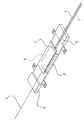
図1は本発明の一実施の形態を示す外観斜視図である。尚、従来例と同様の部材には共通の符号を用いた。
【0025】
図1に示すように光ファイバ1が導波路素子2に融着接続され、導波路素子2が非金属弾性体を介して台座3に固定されている。台座3はパッケージ4と一体的に形成されていてもよく、また別体に形成されてねじ止め等により固定されていてもよい。非金属弾性体としては、シリコーン系樹脂の接着剤が好ましい。光ファイバ1はパッケージ4内に形成されたスロット5内に樹脂で固定されている。パッケージ4の側面には長手方向に沿って素子固定用基準壁6が形成されている。素子固定用基準壁6の前後(光ファイバ側)にはストッパ10a,10bが設けられ、導波路素子2が素子固定用基準壁6に押しあてられている。
【0026】
ストッパ10a,10bの間隔Sは、導波路素子2の長手方向の長さL以上、導波路素子2の長さに2mmを加えた値以下である。
【0027】
ここで、ストッパ10a,10bの間隔Sが導波路素子2の長さLより狭いと、導波路素子2を素子固定用規準壁6に押しあてることができなくなってしまう。また、導波路素子2の長さLに2mmを加えた値以上の値になると、導波路素子2が許容固定範囲からはみ出してしまい、融着部7からスロット5までの距離と融着部12からスロット13までの距離が不均等となってしまう。そのため、JIS等で示されている最も厳しい振動試験(10〜2000Hz)を行うと、融着部7(12)からスロット5(13)までの距離が長い方の光ファイバ1が共振し、ついには光ファイバ1が融着部で破断してしまう。
【0028】
以上の点よりストッパ10a,10bの間隔Sは導波路素子2の長手方向の長さL以上であり、導波路素子2の長さLに2mmを加えた値以下でなければならない。
【0029】
本発明の光モジュールは、素子固定用規準壁6の長手方向の前後に、導波路素子2が前後方向に移動するのを規制するためのストッパ10a,10bが設けられているので、パッケージ4を10〜2000Hzの範囲で振動試験を行っても光ファイバ1が共振することがなく、しかも融着部7,12で光ファイバ1が破断することがなかった。
【0030】
以上において、本発明の光モジュールは、導波路素子を確実に許容された位置に固定することができ、外部からの振動に強い光モジュールを提供することができる。
【0031】
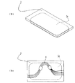
図2は本発明の光モジュールの他の実施の形態を説明するための説明図であり、図2(a)は処理前を示し、図2(b)は処理後を示している。尚、説明を簡単にするため金属パッケージは省略されている。
【0032】
導波路素子2に融着された光ファイバ1は、融着部7から3〜5mmまでの部分1aが除去されている(図2(a))。
【0033】
光ファイバ1の被覆が除去された部分1aに、ヤング率が0.1Kgf/mm2 以下の樹脂15がコーティングされる。コーティングは光ファイバ1を導波路素子2に融着した直後に行われる(図2(b))。
【0034】
被覆が除去された光ファイバ1に樹脂15をコーティングしたところ、実装中に光ファイバ1が傷付くことがなく、プルーフ試験で光ファイバ1が破断することもなく、長期的な信頼性を保証することができる。
【0035】
図3は本発明の光モジュールの他の実施の形態を説明するための説明図であり、図3(a)は導波路素子の外観斜視図であり、図3(b)は導波路素子の平面図である。尚、説明を簡単にするため金属パッケージは省略されている。
【0036】
図3(a)及び図3(b)に示すようにコの字形状の台座16上に導波路素子2として導波路アレイ素子がシリコーン系樹脂の接着剤により接着固定されている。導波路素子2は導波路アレイ部8以外の部分で台座16に接着固定されている。
【0037】
このような光モジュールは、導波路アレイ部8が台座16に固定されていないので、台座16に応力が加わっても導波路アレイ部8に応力が加わることがなくなり、光学特性の劣化が防止され、信頼性が向上する。
【0038】
尚、コの字形状の台座16を用いる代わりに従来と同様の台座上にコの字形状に接着剤を塗布してもよい。
【0039】
【発明の効果】
以上要するに本発明によれば、次のような優れた効果を発揮する。
【0040】
(1) 導波路素子が素子固定用基準壁と前後二つのストッパとで固定される場合には導波路素子の固定位置が規制されるので、許容固定位置の範囲からはみ出たり、光ファイバが振動で破断することがなくなり、信頼性が向上する。
【0041】
(2) 光ファイバの被覆が除去された部分を樹脂でコーティングした場合には、光ファイバの被覆が除去された部分が保護されるので、実装中に光ファイバに傷が付くことがなくなり、プルーフ試験で光ファイバが破断することがなくなり、信頼性が向上する。
【0042】
(3) 導波路素子が導波路アレイ部以外の部分で台座に接着固定されている場合には、導波路アレイ部が台座に固定されていないので、台座に加わった応力が導波路アレイ部に加わることがなくなり、光学特性の変化が防止され、信頼性が向上する。
【図面の簡単な説明】
【図1】本発明の一実施の形態を示す外観斜視図である。
【図2】本発明の光モジュールの他の実施の形態を説明するための説明図である。
【図3】本発明の光モジュールの他の実施の形態を説明するための説明図である。
【図4】光モジュールの従来例を示す外観斜視図である。
【図5】光モジュールの他の従来例を示す外観斜視図である。
【図6】光モジュールの他の従来例を示す外観斜視図である。
【符号の説明】
1 光ファイバ
2 導波路素子
4 パッケージ
6 素子固定用基準壁
8 導波路アレイ部
10a,10b ストッパ
16 台座[0001]
BACKGROUND OF THE INVENTION
The present invention relates to an optical module used for optical fiber communication.
[0002]
[Prior art]
One of optical components used for optical fiber communication is an optical module.
[0003]
FIG. 4 is an external perspective view showing a conventional example of an optical module.
[0004]
The
[0005]
FIG. 5 is an external perspective view showing another conventional optical module.
[0006]
As shown in the figure, the
[0007]
FIG. 6 is an external perspective view showing another conventional optical module.
[0008]
The
[0009]
[Problems to be solved by the invention]
Incidentally, since the optical module shown in FIG. 4 has no reference for the longitudinal position of the
[0010]
Further, in the optical module shown in FIG. 5, the slot 5 for fixing the
[0011]
Furthermore, although the optical module shown in FIG. 6 is fixed to the
[0012]
Therefore, an object of the present invention is to solve the above-described problems and provide a highly reliable optical module.
[0013]
[Means for Solving the Problems]
To achieve the above object, the present invention provides a metal package, a pedestal formed on the metal package, a waveguide element fixed to the pedestal via a non-metallic elastic body, and fixed to the waveguide element. An optical module , wherein the optical fiber is fixed to a slot formed in a longitudinal direction of the metal package ,
The metal package is provided on the side surface of the metal package along the longitudinal direction with the element fixing reference wall and the longitudinal direction of the waveguide element in the longitudinal direction and provided at a position spaced from the slot. And a convex stopper that restricts the longitudinal movement of the waveguide element.
[0014]
In addition to the above configuration, in the present invention, the distance between the stoppers is preferably not less than the length in the longitudinal direction of the waveguide element and not more than the value obtained by adding 2 mm to the length of the waveguide element.
[0019]
According to the present invention, when the waveguide element is fixed by the element fixing reference wall and the two front and rear stoppers, the fixed position of the waveguide element is regulated, so that it does not protrude from the range of the allowable fixed position. , Position accuracy is increased and reliability is improved.
[0020]
When the distance between the stoppers is not less than the length in the longitudinal direction of the waveguide element and not more than the value obtained by adding 2 mm to the length of the waveguide element, the most severe vibration test specified in JIS standard is performed. However, it can withstand without resonating, and the reliability is improved.
[0021]
When the part from which the optical fiber coating is removed is coated with resin, the optical fiber coating is removed so that the optical fiber is not damaged during mounting. The fiber is not broken and the reliability is improved.
[0022]
When the waveguide element is bonded and fixed to the pedestal at a portion other than the waveguide array portion, the waveguide array portion is not fixed to the pedestal, so that stress applied to the pedestal may be applied to the waveguide array portion. The change in optical characteristics is prevented, and the reliability is improved.
[0023]
DETAILED DESCRIPTION OF THE INVENTION
Hereinafter, embodiments of the present invention will be described in detail with reference to the accompanying drawings.
[0024]
FIG. 1 is an external perspective view showing an embodiment of the present invention. In addition, the same code | symbol was used for the member similar to a prior art example.
[0025]
As shown in FIG. 1, an
[0026]
The distance S between the
[0027]
Here, if the distance S between the
[0028]
From the above points, the distance S between the
[0029]
The optical module of the present invention is provided with
[0030]
As described above, the optical module of the present invention can provide an optical module that can reliably fix the waveguide element at a permitted position and is resistant to vibration from the outside.
[0031]
2A and 2B are explanatory views for explaining another embodiment of the optical module of the present invention. FIG. 2A shows a state before processing, and FIG. 2B shows a state after processing. Note that the metal package is omitted for the sake of simplicity.
[0032]
The
[0033]
The
[0034]
When the
[0035]
FIG. 3 is an explanatory diagram for explaining another embodiment of the optical module of the present invention, FIG. 3 (a) is an external perspective view of the waveguide element, and FIG. 3 (b) is an illustration of the waveguide element. It is a top view. Note that the metal package is omitted for the sake of simplicity.
[0036]
As shown in FIGS. 3A and 3B, a waveguide array element is bonded and fixed as a
[0037]
In such an optical module, since the waveguide array portion 8 is not fixed to the
[0038]
Instead of using the
[0039]
【The invention's effect】
In short, according to the present invention, the following excellent effects are exhibited.
[0040]
(1) When the waveguide element is fixed by the element fixing reference wall and the two front and rear stoppers, the fixed position of the waveguide element is restricted, so that the waveguide element protrudes from the allowable fixed position range or the optical fiber vibrates. This eliminates breakage and improves reliability.
[0041]
(2) When the part from which the optical fiber coating has been removed is coated with resin, the part from which the optical fiber coating has been removed is protected, so that the optical fiber is not damaged during mounting. In the test, the optical fiber is not broken and the reliability is improved.
[0042]
(3) When the waveguide element is bonded and fixed to the pedestal at a portion other than the waveguide array portion, the stress applied to the pedestal is applied to the waveguide array portion because the waveguide array portion is not fixed to the pedestal. It is not added, the change in optical characteristics is prevented, and the reliability is improved.
[Brief description of the drawings]
FIG. 1 is an external perspective view showing an embodiment of the present invention.
FIG. 2 is an explanatory diagram for explaining another embodiment of the optical module of the present invention.
FIG. 3 is an explanatory diagram for explaining another embodiment of the optical module of the present invention.
FIG. 4 is an external perspective view showing a conventional example of an optical module.
FIG. 5 is an external perspective view showing another conventional example of an optical module.
FIG. 6 is an external perspective view showing another conventional example of an optical module.
[Explanation of symbols]
DESCRIPTION OF
Claims (2)
上記金属パッケージは、該金属パッケージの側面に長手方向に沿って形成された素子固定用基準壁と、上記導波路素子の長手方向の前後であり、かつ上記スロットから離間した位置に設けられ上記導波路素子の長手方向の移動を規制する凸状のストッパとを備えたことを特徴とする光モジュール。 A metal package; a base formed on the metal package; a waveguide element fixed to the base via a non-metallic elastic body; and an optical fiber fixed to the waveguide element. Is an optical module fixed to a slot formed in the longitudinal direction of the metal package ,
The metal package is provided on the side surface of the metal package along the longitudinal direction with the element fixing reference wall and the longitudinal direction of the waveguide element in the longitudinal direction and provided at a position spaced from the slot. An optical module comprising a convex stopper for restricting movement of the waveguide element in the longitudinal direction.
Priority Applications (1)
| Application Number | Priority Date | Filing Date | Title |
|---|---|---|---|
| JP32392296A JP3697802B2 (en) | 1996-12-04 | 1996-12-04 | Optical module |
Applications Claiming Priority (1)
| Application Number | Priority Date | Filing Date | Title |
|---|---|---|---|
| JP32392296A JP3697802B2 (en) | 1996-12-04 | 1996-12-04 | Optical module |
Publications (2)
| Publication Number | Publication Date |
|---|---|
| JPH10160960A JPH10160960A (en) | 1998-06-19 |
| JP3697802B2 true JP3697802B2 (en) | 2005-09-21 |
Family
ID=18160130
Family Applications (1)
| Application Number | Title | Priority Date | Filing Date |
|---|---|---|---|
| JP32392296A Expired - Fee Related JP3697802B2 (en) | 1996-12-04 | 1996-12-04 | Optical module |
Country Status (1)
| Country | Link |
|---|---|
| JP (1) | JP3697802B2 (en) |
Families Citing this family (4)
| Publication number | Priority date | Publication date | Assignee | Title |
|---|---|---|---|---|
| JP2001337233A (en) * | 2000-05-26 | 2001-12-07 | Furukawa Electric Co Ltd:The | Array waveguide type diffraction grating module and optical module using it |
| JPWO2012002368A1 (en) * | 2010-07-02 | 2013-08-29 | 古河電気工業株式会社 | Arrayed waveguide grating optical multiplexer / demultiplexer |
| JP5390562B2 (en) | 2011-06-22 | 2014-01-15 | 日本電信電話株式会社 | Planar lightwave circuit |
| JP5922042B2 (en) | 2013-01-10 | 2016-05-24 | Nttエレクトロニクス株式会社 | Optical module |
-
1996
- 1996-12-04 JP JP32392296A patent/JP3697802B2/en not_active Expired - Fee Related
Also Published As
| Publication number | Publication date |
|---|---|
| JPH10160960A (en) | 1998-06-19 |
Similar Documents
| Publication | Publication Date | Title |
|---|---|---|
| JP2706164B2 (en) | Decoupling fiber optical feedthrough assembly | |
| EP1482336A3 (en) | Optical waveguide module having waveguide substrate made of predetermined material and ferrule made of material different from that of waveguide substrate | |
| EP1168536A1 (en) | Optical semiconductor module | |
| US6295398B1 (en) | Asymmetrical miniature bends in optical fibers and method of forming same | |
| JP3697802B2 (en) | Optical module | |
| JP3802844B2 (en) | Optical semiconductor module | |
| JP2005173534A (en) | Ferrule block and optical module using the same | |
| JP2001074982A (en) | Optical coupling device for optical module, and its optical coupling method | |
| JP3824879B2 (en) | Optical module | |
| JP2002341160A (en) | Optical waveguide module packaged component | |
| JP2004511009A (en) | Low stress internal structures for optoelectronic packages | |
| JP2001141645A (en) | Raindrop detecting device | |
| JP3500558B2 (en) | Fixing structure of optical circuit parts | |
| JPH1010372A (en) | Ld module | |
| JP4952219B2 (en) | Optical module | |
| JP4262136B2 (en) | Optical isolator module with transparent window and optical element module | |
| JPH09211276A (en) | Optical module and optical connection device using the same | |
| EP3628540B1 (en) | Windshield sensing device | |
| JP2848355B2 (en) | Package for photodiode | |
| JP2005049816A (en) | Optical waveguide package | |
| JP2877972B2 (en) | Power connector for laser | |
| JPS6029709A (en) | Optical transmission body | |
| JPH095567A (en) | Optical module | |
| JP4497810B2 (en) | Optical element | |
| JP2003195121A (en) | Optical connector |
Legal Events
| Date | Code | Title | Description |
|---|---|---|---|
| A131 | Notification of reasons for refusal |
Free format text: JAPANESE INTERMEDIATE CODE: A131 Effective date: 20040302 |
|
| A521 | Written amendment |
Free format text: JAPANESE INTERMEDIATE CODE: A523 Effective date: 20040506 |
|
| TRDD | Decision of grant or rejection written | ||
| A01 | Written decision to grant a patent or to grant a registration (utility model) |
Free format text: JAPANESE INTERMEDIATE CODE: A01 Effective date: 20050614 |
|
| A61 | First payment of annual fees (during grant procedure) |
Free format text: JAPANESE INTERMEDIATE CODE: A61 Effective date: 20050627 |
|
| R150 | Certificate of patent or registration of utility model |
Free format text: JAPANESE INTERMEDIATE CODE: R150 |
|
| S531 | Written request for registration of change of domicile |
Free format text: JAPANESE INTERMEDIATE CODE: R313531 |
|
| R350 | Written notification of registration of transfer |
Free format text: JAPANESE INTERMEDIATE CODE: R350 |
|
| FPAY | Renewal fee payment (event date is renewal date of database) |
Free format text: PAYMENT UNTIL: 20090715 Year of fee payment: 4 |
|
| LAPS | Cancellation because of no payment of annual fees |