JP3681528B2 - Graphic processor and data processing system - Google Patents
Graphic processor and data processing system Download PDFInfo
- Publication number
- JP3681528B2 JP3681528B2 JP35254397A JP35254397A JP3681528B2 JP 3681528 B2 JP3681528 B2 JP 3681528B2 JP 35254397 A JP35254397 A JP 35254397A JP 35254397 A JP35254397 A JP 35254397A JP 3681528 B2 JP3681528 B2 JP 3681528B2
- Authority
- JP
- Japan
- Prior art keywords
- pixel data
- command
- information
- weighted average
- image information
- Prior art date
- Legal status (The legal status is an assumption and is not a legal conclusion. Google has not performed a legal analysis and makes no representation as to the accuracy of the status listed.)
- Expired - Fee Related
Links
Images


Classifications
-
- G—PHYSICS
- G06—COMPUTING; CALCULATING OR COUNTING
- G06T—IMAGE DATA PROCESSING OR GENERATION, IN GENERAL
- G06T15/00—3D [Three Dimensional] image rendering
- G06T15/005—General purpose rendering architectures
-
- G—PHYSICS
- G09—EDUCATION; CRYPTOGRAPHY; DISPLAY; ADVERTISING; SEALS
- G09G—ARRANGEMENTS OR CIRCUITS FOR CONTROL OF INDICATING DEVICES USING STATIC MEANS TO PRESENT VARIABLE INFORMATION
- G09G5/00—Control arrangements or circuits for visual indicators common to cathode-ray tube indicators and other visual indicators
- G09G5/36—Control arrangements or circuits for visual indicators common to cathode-ray tube indicators and other visual indicators characterised by the display of a graphic pattern, e.g. using an all-points-addressable [APA] memory
- G09G5/363—Graphics controllers
-
- G—PHYSICS
- G09—EDUCATION; CRYPTOGRAPHY; DISPLAY; ADVERTISING; SEALS
- G09G—ARRANGEMENTS OR CIRCUITS FOR CONTROL OF INDICATING DEVICES USING STATIC MEANS TO PRESENT VARIABLE INFORMATION
- G09G2340/00—Aspects of display data processing
- G09G2340/10—Mixing of images, i.e. displayed pixel being the result of an operation, e.g. adding, on the corresponding input pixels
-
- G—PHYSICS
- G09—EDUCATION; CRYPTOGRAPHY; DISPLAY; ADVERTISING; SEALS
- G09G—ARRANGEMENTS OR CIRCUITS FOR CONTROL OF INDICATING DEVICES USING STATIC MEANS TO PRESENT VARIABLE INFORMATION
- G09G5/00—Control arrangements or circuits for visual indicators common to cathode-ray tube indicators and other visual indicators
- G09G5/36—Control arrangements or circuits for visual indicators common to cathode-ray tube indicators and other visual indicators characterised by the display of a graphic pattern, e.g. using an all-points-addressable [APA] memory
- G09G5/39—Control of the bit-mapped memory
- G09G5/393—Arrangements for updating the contents of the bit-mapped memory
-
- G—PHYSICS
- G09—EDUCATION; CRYPTOGRAPHY; DISPLAY; ADVERTISING; SEALS
- G09G—ARRANGEMENTS OR CIRCUITS FOR CONTROL OF INDICATING DEVICES USING STATIC MEANS TO PRESENT VARIABLE INFORMATION
- G09G5/00—Control arrangements or circuits for visual indicators common to cathode-ray tube indicators and other visual indicators
- G09G5/36—Control arrangements or circuits for visual indicators common to cathode-ray tube indicators and other visual indicators characterised by the display of a graphic pattern, e.g. using an all-points-addressable [APA] memory
- G09G5/39—Control of the bit-mapped memory
- G09G5/399—Control of the bit-mapped memory using two or more bit-mapped memories, the operations of which are switched in time, e.g. ping-pong buffers
-
- H—ELECTRICITY
- H04—ELECTRIC COMMUNICATION TECHNIQUE
- H04N—PICTORIAL COMMUNICATION, e.g. TELEVISION
- H04N7/00—Television systems
- H04N7/01—Conversion of standards, e.g. involving analogue television standards or digital television standards processed at pixel level
- H04N7/0127—Conversion of standards, e.g. involving analogue television standards or digital television standards processed at pixel level by changing the field or frame frequency of the incoming video signal, e.g. frame rate converter
- H04N7/0132—Conversion of standards, e.g. involving analogue television standards or digital television standards processed at pixel level by changing the field or frame frequency of the incoming video signal, e.g. frame rate converter the field or frame frequency of the incoming video signal being multiplied by a positive integer, e.g. for flicker reduction
Landscapes
- Engineering & Computer Science (AREA)
- Computer Graphics (AREA)
- Physics & Mathematics (AREA)
- General Physics & Mathematics (AREA)
- Theoretical Computer Science (AREA)
- Computer Hardware Design (AREA)
- Controls And Circuits For Display Device (AREA)
- Picture Signal Circuits (AREA)
Description
【0001】
【発明の属する技術分野】
本発明は、ノンインタレース走査による表示に向けられた画像情報をインタレース走査で表示するときに発生する虞のあるフリッカ(ちらつき)を防止する技術に関し、例えばコンピュータのディスプレイに対する表示及び描画制御を行なうグラフィックプロセッサ、更にはそのようなグラフィックプロセッサを用いたデータ処理システムに適用して有効な技術に関するものである。
【0002】
【従来の技術】
パーソナルコンピュータなどのコンピュータ装置に設けられたグラフィックプロセッサは、アプリケーションプログラムによって作成された画像データをディスプレイの表示タイミングに同期させビデオ信号としてディスプレイに供給する。コンピュータ装置ではノンインタレース走査でディスプレイを制御する。ノンインタレース走査方式は、走査フィールドの飛び越し走査を行なわず、毎回全ての走査線を走査して、1回の垂直走査期間で1画面を形成できるため、ちらつきの少ない良好な表示品質を得ることができる。
【0003】
一方テレビ等に採用されているインタレース走査方式は走査線を奇数フィールドと偶数フィールドに分け、垂直走査期間毎に、片方のフィールドのみを走査、即ち走査線を1本置きに飛び越し走査して、2回の垂直走査期間で1画面を形成する方式である。
【0004】
前記ノンインタレース走査方式では毎垂直走査期間毎に全ての走査線を走査するから走査された走査線の垂直方向の位置はどの画面でも同じである。しかしながら、インタレース走査方式では、奇数フィールドの走査線から成る画面と偶数フィールドの走査線から成る画面とを、垂直走査期間毎に交互に表示するから、表示に供される走査線の垂直位置は連続する前後の画面間で1走査線分ずれることになる。このため、インタレース走査方式では隣接する走査線の画像情報の差異(輝度若しくは色等の差異)が大きいと、偶数フィールド画面と奇数フィールド画面との間でちらつきを生じ易くなる。
【0005】
ところで、パーソナルコンピュータで作成された高解像度の画像データをNTSC(National Television System Committee )方式等のビデオ信号に変換することによって通常のテレビジョンセットにも表示させたいというニーズがある。しかしながら、走査方式を変えるだけでそのままコンピュータ画像をテレビジョンセットに表示させると、ノンインタレース走査方式のディスプレイに表示する場合と異なり、画面にちらつきが発生する。これは、テレビやビデオカメラ或いはVTRなどによる自然画に比べると、コンピュータ画像は主に文字などの線やシェードパターンで構成され、上下隣接する走査線間で画像情報の差異が大きいからである。例えば、上下隣接する走査線上の同一縦方向位置の画素が黒、白、黒のように輝度に大きな差異がある場合、当該画素部分の黒と白は2画面で表示され、これによってちらつきを生ずる。
【0006】
そのようなちらつきを防止する技術は、特開平6−83299、特開平7−274086、特開平6−46299、特開平8−317311の各号公報に記載が有る。それら技術は細部において夫々相違が有るが、何れも、表示制御系において走査線毎に画像情報を格納するラインバッファを複数走査線分用意し、複数本のラインバッファには現在の走査線の画像情報と共に其の前の走査線上の画像情報を蓄え、現走査線上の画素データを前の走査線上の対応位置の画素データを用いて補正し、走査線間で画像情報の差異が大きくならないようにするものである。
【0007】
【発明が解決しようとする課題】
ラインバッファは表示タイミングに同期して動作されなければならないから、ラインバッファには高速SRAM(スタティック・ランダム・アクセス・メモリ)などを用いなければならない。このとき、従来技術はラインバッファを複数本必要とするから、表示制御回路更にはグラフィック制御回路のコストを上昇させてしまう。また、表示制御系で前記ちらつきを防止する技術は、既に描画が完了されてフレームバッファに格納された画像データを表示走査に同期して出力するとき補正処理を行なうものであり、描画前のソース画像に着目してちらつき防止の処理を行なったり、その処理の度合いを任意に決定したりするという自由度について考慮されていない。
【0008】
本発明の目的は、隣接する走査線の画像情報の差異をラインバッファを増やすことなく緩和することができるグラフィックプロセッサ及びデータ処理システムを提供することになる。
【0009】
本発明の別の目的は、ノンインタレース走査表示に向けられた画像情報をインタレース走査で表示するときに発生する虞のあるちらつきの防止を、ラインバッファの数を増やすことなく実現できるグラフィックプロセッサ及びデータ処理システムを提供することにある。
【0010】
本発明の他の目的は、解像度の異なる画像情報をオーバーレイしてインタレース走査で表示したとき解像度の相違による画面のちらつきを防止する処理を自由に行なうことができるグラフィックプロセッサ及びデータ処理システムを提供することにある。
【0011】
本発明の他の目的は、ちらつき防止のための命令を有する低コストなグラフィックプロセッサを提供することにある。
【0012】
本発明の他の目的は、フレームバッファメモリでちらつき防止のための画像データ処理を行なうことが可能なデータ処理システムを提供することにある。
【0013】
本発明の前記並びにその他の目的と新規な特徴は本明細書の記述及び添付図面から明らかになるであろう。
【0014】
【課題を解決するための手段】
本願において開示される発明のうち代表的なものの概要を簡単に説明すれば下記の通りである。
【0015】
本発明の第1の観点によるグラフィックプロセッサ(1)は、例えば図1に例示されるように、コマンドの解読結果に従って画素データをフレームバッファとしてのメモリ(4)に描画するための制御を行なう描画制御手段(2)と、メモリに描画された画素データを表示走査のタイミングに同期して走査方向に読み出す制御を行なう表示制御手段(3)とを含む。前記描画制御手段は、画素の配列に対応して画素データが配列されたソース画像情報の画素データを、前記走査方向とは直交する方向に隣接する画素データと加重平均を行なって、前記ソース画像情報を補正するブレンド処理を実行可能である。グラフィックプロセッサに対しては、ブレンド処理を行うためのコマンド(命令)が定義されている。ブレンド処理において、隣接する画素データを用いて加重平均を行なうことにより、隣接する走査線間で画像情報の差異が大きい場合にもその差異を緩和する事ができる。このとき、描画制御手段はメモリから画素データを前記走査方向とは直交する方向に順次読み出して加重平均を行なえばよく、描画制御手段はもとより表示制御手段にもラインバッファのような記憶手段を新たに増設することを要しない。これにより、隣接する走査線の画像情報の差異をラインバッファを増やすことなく緩和することができる。そのようにして、ブレンド処理された画像情報をインタレース走査形式で表示しても、不所望なちらつきは発生しない。
【0016】
グラフィックプロセッサにちらつき防止の為の命令をもたせることによって、低コストでちらつき防止が可能なグラフィックプロセッサが提供できる。
【0017】
本発明の第2の観点によるグラフィックプロセッサは、コマンドの解読結果に従って画素データをメモリに描画するための制御を行なう描画制御手段と、メモリに描画された画素データを表示走査のタイミングに同期して走査方向に読み出す制御を行なう表示制御手段とを含み、前記描画制御手段は、画素の配列に対応して画素データが配列されたソース画像情報の所在を示すソース指定情報と、前記ソース指定情報で示されるソース画像情報の画素データを前記走査方向とは直交する方向に隣接する画素データと加重平均を行なうことを指示するコマンド情報と、加重平均された画素データを格納する所在を示すディスティネーション指定情報とを有するブレンド処理コマンドを実行可能である。これにより、前記描画制御手段は、画素の配列に対応して画素データが配列されたソース画像情報の画素データを前記メモリから読み込み、読み込んだ画素データを前記走査方向とは直交する方向に隣接する他の画素データと加重平均して前記メモリに書き戻すという、リード・モディファイ・ライトのような処理を行なうことによってブレンド処理を実行することができる。したがって、描画制御手段はもとより表示制御手段にもラインバッファのような記憶手段を新たに増設することを要せず、隣接する走査線間で画像情報の差異が大きい場合にもその差異を緩和することができる。
【0018】
ブレンド処理コマンドにおけるソース指定情報とディスティネーション指定情報とを任意に指定できるので、表示領域に対してブレンド処理を施す領域を任意に決定できるという自由度を得ることができる。例えば、自然画とコンピュータ画像とをオーバーレイするとき、コンピュータ画像に対してだけブレンド処理を施す事ができる。したがって、必要な部分の画像情報に対してだけブレンド処理を行なうことができ、無駄な処理を省くことができ、ブレンド処理時間の短縮と画質向上との双方を実現できる。
【0019】
前記ブレンド処理コマンドは更に、前記加重平均を行なう対象を、前記走査方向とは直交する方向に隣接する前後双方の画素データとするか、又は前記走査方向とは直交する方向に隣接する前後何れか一方の画素データとするかを指定する第1の属性情報を有することができる。過度な加重平均が行なわれると逆に画像がぼけてしまう虞もあるので、ブレンド処理対象とされるソースデータの特性に応じて加重平均の度合いを選択できる。これによって、高品質なちらつき防止を実現する。
【0020】
また、前記ブレンド処理コマンドは更に、前記ディスティネーション指定情報で指定される領域のうちクリッピング領域に含まれる領域に対してだけ前記加重平均された画像データを格納することを指示する第2の属性情報を有することができる。これにより、ディスティネーション指定情報に加えて、クリッピング領域も使用でき、ブレンド処理の操作性若しくはグラフィックプロセッサの使い勝手を更に向上させることができる。
【0021】
本発明の第3の観点によるデータ処理システムは、中央処理装置と、グラフィックプロセッサと、フレームバッファとしてのメモリ手段と、ディスプレイとを含む。前記グラフィックプロセッサは、前記中央処理装置が発行するコマンドの解読結果に従って画素データを前記メモリ手段に描画する制御を行なう描画制御手段と、前記メモリ手段に描画された画素データを前記ディスプレイによる表示走査のタイミングに同期して走査方向に読み出し前記ディスプレイに与える制御を行なう表示制御手段とを含む。前記描画制御手段は、画素の配列に対応して画素データが配列されたソース画像情報の画素データを前記メモリ手段から読み込み、読み込んだ画素データを前記走査方向とは直交する方向に隣接する他の画素データと加重平均して前記メモリ手段に書き戻すブレンド処理を実行可能である。これにより、グラフィックプロセッサは、リード・モディファイ・ライトのような処理を行なうことによってブレンド処理を実行し、メモリ手段上の画像データを処理することができる。したがって、描画制御手段はもとより表示制御手段にもラインバッファのような記憶手段を新たに増設することを要せず、隣接する走査線間で画像情報の差異が大きい場合にもその差異を緩和することができる。
【0022】
前記中央処理装置は前記グラフィックプロセッサに前記ブレンド処理を実行させるためにブレンド処理コマンドを発行可能であり、該ブレンド処理コマンドは、画素の配列に対応して画素データが配列されたソース画像情報の所在を示すソース指定情報と、前記ソース指定情報で示されるソース画像情報の画素データを前記走査方向とは直交する方向に隣接する画素データと加重平均を行なうことを指示するコマンド情報と、加重平均された画素データを格納する所在を示すディスティネーション指定情報とを含むことができる。
【0023】
前記ブレンド処理コマンドは更に第1の属性情報を含むことができる。このとき、前記描画制御手段は、前記第1の属性情報の値に応じて、前記加重平均を行なう対象を、前記走査方向とは直交する方向に隣接する前後双方の画素データとするか、又は前記走査方向とは直交する方向に隣接する前後何れか一方の画素データとするかを決定する。また、前記ブレンド処理コマンドは更に第2の属性情報を含むことができる。このとき、前記描画制御手段は、前記中央処理装置によってクリッピング領域の指定情報が設定されるクリッピングレジスタを有し、前記第2の属性情報が第1の状態では前記ディスティネーション指定情報で指定される領域のうちクリッピング領域に含まれる領域に対してだけ前記加重平均された画像データを格納し、前記第2の属性情報が第2の状態ではクリッピング領域を無視し前記ディスティネーション指定情報で指定される領域に前記加重平均された画像データを格納する。これにより、描画前のソース画像の特徴に着目してちらつき防止の処理の度合いを任意に決定したり、ディスティネーション指定情報とクリッピング領域との双方を利用してブレンド処理を行なうことができるという自由度を達成できる。
【0024】
上記の様にグラフィックプロセッサにちらつき防止用の命令を設けることで、ソフトウェア的にちらつき防止を行なうことができる。このことは、1つのグラフィックプロセッサの用途を複数のデータ処理システムに向けられることを意味する。
【0025】
【発明の実施の形態】
《データ処理システム》
図2には本発明の一例に係るデータ処理システムのブロック図が示される。アドレス、データ及び制御信号の各信号線を含むシステムバス5には、代表的に示されたマイクロプロセッサ若しくはマイクロコンピュータのようなCPU(中央処理装置)6、メモリ7、及びグラフィックプロセッサ1が結合されている。前記メモリ7はCPU6の作業領域若しくはデータ一時記憶領域として利用される所謂メインメモリを構成する。前記CPU6とグラフィックプロセッサ1の夫々は、単結晶シリコンのような1個の半導体基板に形成されて、別々に半導体集積回路化されている。
【0026】
図示されたデータ処理システムが例えばナビゲーションシステムに適用される場合、前記システムバス5には地図データをアクセスするための図示を省略するドライブ装置のインタフェース回路や位置検出回路とのインタフェース回路などが接続される。また、図示されたデータ処理システムがインタネットテレビに適用される場合、前記システムバス5には図示を省略するモデム若しくはターミナルアダプタなどが接続される。
【0027】
前記グラフィックプロセッサ1にはローカルメモリとしてユニファイドメモリ4が結合される。このユニファイドメモリ4は、コマンド領域、フレームバッファ領域、及び図形などの基礎データ(テキスチャー)領域などに利用される統合メモリであり、例えばシンクロナスDRAM(ダイナミック・ランダム・アクセス・メモリ)によって構成される。
【0028】
前記グラフィックプロセッサ1は、CPU6から発行されユニファイドメモリ4に書き込まれたるコマンドの解読結果に従って画素データをユニファイドメモリ4に描画するための制御や、ユニファイドメモリ4に描画された画素データを表示走査のタイミングに同期して走査方向に読み出す表示制御などを行なう。
【0029】
表示タイミングに同期してグラフィックプロセッサ1から出力される画像データは、特に制限されないが、1画素18ビットのディジタルRGBデータ10とされる。ディジタルRGBデータ10はD/Aコンバータ11でアナログRGB信号12に変換される。また、ディジタルRGBデータ10はミキサ13で外部ビデオ信号14と合成可能にされ、ミキサ13の出力信号はディジタルビデオエンコーダ15でNTSC規格に準拠したテレビジョン信号としてのアナログNTSC信号16にアナログ変換される。図2に示されるディスプレイ17がVGA(Video Graphics Array)又はSVGA(Supper VGA)等のアナログモニタである場合、前記アナログRGB信号12が当該モニタに供給される。ディスプレイ17がテレビジョンセットのモニタである場合にはアナログNTSC信号16が当該モニタに供給される。また、ディスプレイ17がナビゲーションシステムのディジタルモニタである場合には当該モニタにはディジタルRGB信号が直接供給される。尚、前記D/Aコンバータ11をグラフィックプロセッサ1に内蔵させれば、半導体集積回路化されたグラフィックプロセッサ1の外部端子(ピン)数削減に効果的である。
【0030】
《グラフィックプロセッサ》
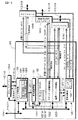
図3には前記グラフィックプロセッサ1の一例が示される。グラフィックプロセッサ1は、描画制御手段(2)を構成するレンダリングユニット100及びレンダリングバッファ101と、表示制御手段(3)を構成するディスプレイユニット102及びディスプレイバッファユニット103とを有する。前記ディジタルRGBデータ10はディスプレイユニット102からI/Oバッファ104を介して外部に出力される。CPU6とのインタフェース制御はCPUインタフェースユニット105が行い、前記ユニファイドメモリ4に対する外部インタフェース制御はメモリインタフェースユニット106が行なう。前記CPU6は前記システムバス5を介してI/Oバッファ107に接続され、前記ユニファイドメモリ4はI/Oバッファ108に接続される。CLK0はグラフィックプロセッサの動作基準クロック信号であり、CLK1は垂直同期信号、水平同期信号及びドットクロック信号などを総称する表示タイミング信号である。クロックパルスジェネレータ(CPG0)115はクロック信号を分周したりして各種内部同期信号を形成する。クロックパルスジェネレータ(CPG1)116は前記表示タイミング信号に基づいてディスプレイユニット102などの表示制御系をディスプレイに同期させる内部タイミング信号を形成する。
【0031】
前記レンダリングバッファユニット101は外部のユニファイドメモリ4とレンダリングユニット100との間のバッファとされ、ユニファイドメモリ4のフレームバッファに対するリード・ライトデータ、ユニファイドメモリ4から読み出されたコマンド、そしてユニファイドメモリ4から読み出されたテキスチャーなどを一時的に格納する。前記ディスプレイバッファユニット103はユニファイドメモリ4とディスプレイユニット102との間のバッファとされ、ユニファイドメモリ4のフレームバッファ領域から読み出された画像情報を一時的に格納してディスプレイユニット102に渡す。更にディスプレイバッファユニット103はカラーパレット1031を有し、1画素8ビットの画像データを1画素16ビットの画像データに変換する。前記CPUインタフェースユニット105はDMA(ダイレクト・メモリ・アクセス)制御回路1051及びデータフォーマット変換回路1052などを有する。データフォーマット変換回路1052はディジタルビデオフォーマットYUV(Yは輝度、U/Vは色差成分)又はナビゲーションシステム用のディジタルビデオフォーマットΔYUVをRGB(レッド、グリーン、ブルー)フォーマットのデータに変換する回路である。
【0032】
前記CPUインタフェースユニット105、レンダリングユニット100、ディスプレイバッファニット103及びI/Oバッファ107はCPUデータバス110を共有し、CPU6からI/Oバッファ107に供給されたアドレス信号はCPUアドレスバス111を介してCPUインタフェースユニット105、レンダリングユニット100及びディスプレイバッファニット103に供給される。これによってCPU6はCPUインタフェースユニット105のDMA制御回路1051、レンダリングユニット100及びディスプレイバッファユニット103のカラーパレット1031などに対する制御情報の初期設定等を行なうことができる。
【0033】
前記CPUインタフェースユニット105、レンダリングバッファユニット101、ディスプレイバッファニット103及びI/Oバッファ108はメモリデータバス112を共有し、CPUインタフェースユニット105又はレンダリングバッファユニット101から出力されるアドレス信号はメモリアドレスバス113を介してメモリインタフェースユニット106に供給され、これに基づいてメモリインタフェースユニット106はユニファイドメモリ4に対するインタフェース制御を行なう。
【0034】
レンダリングユニット100は、レンダリングバッファユニット101
、メモリデータバス112、メモリアドレスバス113及びメモリインタフェースユニット106を介してユニファイドメモリ4に対するリード・ライトを行なう。ユニファイドメモリ4のフレームバッファ領域からディスプレイバッファユニット103への画像データの転送は、特に制限されないが、DMA制御回路1051が行なう。
【0035】
ユニファイドメモリ4に対するコマンド列やテキスチャーの書き込みはDMA制御回路1051がCPU6による初期設定に従ってメモリアドレスバス113及びメモリデータバス112を介して行なうことができる。
【0036】
《レンダリングユニット》
図4には前記レンダリングユニット100及びレンダリングバッファユニット101の一例が示される。コマンドバッファ101A、ワークバッファ101B、ソースバッファ101C及びライトバッファ101Dはレンダリングバッファユニット101に含まれている。レンダリングユニット100は、コマンド制御部120、前処理演算部121、アドレス演算部122、及び画素演算部123に大別することができる。
【0037】
前記コマンド制御部120はコマンドフェッチ、コマンドデコード、及びパラメータ転送の各制御を行なう。レンダリングユニット100が実行するコマンドはユニファイドメモリ4に格納されている。ユニファイドメモリ4に格納されているコマンドは、特定の描画タスクを指示するための複数のコマンドのコマンド列とされる。前述のようにそのようなコマンド列は予めCPU6によって発行され、CPUインタフェースユニット105を介して所定のアドレス領域(コマンド領域)に格納されている。コマンド制御部120は前記コマンド領域の先頭アドレスが設定されるコマンド列開始アドレスレジスタ1201、システム制御レジスタ1202及びステータスレジスタ1203などを有する。コマンド列開始アドレスレジスタ1201及びシステム制御レジスタ1202はCPU6によって初期設定される。前記システム制御レジスタ1202は、コマンド列の実行開始を指示するスタートビットSB、コマンドの実行中断を指示する中断指示ビットRBRK等を有する。ステータスレジスタ1203は実行開始されたコマンド列の最後のコマンドの実行完了によってイネーブルにされる実行完了ビットTRA、コマンド実行の中断指示によって実際にコマンドの実行を中断したときイネーブルにされる中断完了ビットBRK等を含む。CPU6は、予めコマンド列をコマンドバッファ4に書き込ませた後、当該コマンド列の先頭アドレスを前記コマンド列開始アドレスレジスタ1201に設定する。そして、システム制御レジスタ1202のスタートビットSBをイネーブルに設定する。これにより、コマンド制御部120はコマンド列開始アドレスレジスタ1201のアドレスに従ってユニファイドメモリ4からコマンドバッファ101Aにコマンドを読み出し、これを順次フェッチし、フェッチしたコマンドを解読してレンダリングユニット100の内部を制御する。実行開始されたコマンド列の最終コマンドの実行完了は前記実行完了ビットTRAによってCPU6に伝えられる。コマンド列の実行開始後、CPU6が中断指示ビットRBRKを書き換えてコマンド実行の中断を指示したとき、CPU6は中断完了ビットBRKのイネーブルを検出することによって、レンダリングユニット100を別の描画タスクの実行に分岐させる処理を行なうことができる。
【0038】
前処理演算部121はコマンド制御部120で解読されたコマンドコード並びにコマンド引数(例えばポリゴン指定座標、パターンの色など)に従って、例えばポリゴンの左右側辺の端点の座標を抽出する側辺処理などの前処理を行なう。
【0039】
前記アドレス演算部122は、パラメータレジスタファイル1221、テキスチャ画像制御部1222、及び描画アドレス制御部1223などを有する。
【0040】
パラメータレジスタファイル1221はシステムクリッピング領域を指定するシステムクリッピング領域指定レジスタ1221Aや、ユーザクリッピング領域を指定するユーザクリッピング領域指定レジスタ1221B等を有する。それらレジスタにはCPU6から出力されるパラメータが、コマンド制御部120のパラメータ転送制御を介して初期設定される。
【0041】
テキスチャ画像制御部1222は描画に利用するソースデータのアドレス演算等を行なう。演算されたソースデータのアドレスはソースバッファ101Cを介してユニファイドメモリ4に与えられ、それによってアクセスされたソースデータがソースバッファ101Cに一時的に格納される。
【0042】
前記描画アドレス制御部1223は描画アドレスやワークデータのアドレスのような画素アドレスを演算する。例えば前記側辺処理にて得られた側辺の端点を水平に結ぶ位置の各画素の座標を演算する。
【0043】
前記画素演算部123は画素アドレスに対応する画素データの演算を行なう。画素データの演算には、ユニファイドメモリ4からワークバッファに取得されたワークデータやソースバッファに取得されたソースデータなどを用いて行なわれる。演算された画素データはユニファイドメモリ4のフレームバッファ領域への描画のためにライトバッファ101Dに出力される。
【0044】
この画素演算部123で行なわれる画素演算は、2値データの多値データへの変換、塗りつぶし等である。更に、その詳細は後述するが、ブレンドモジュール130により、ソース画像情報を補正するブレンド処理を実行可能である。ブレンド処理は、隣接する画素データを用いて加重平均を行なうことにより、隣接する走査線間で画像情報の差異が大きい場合にもその差異を緩和できるようにする処理である。
【0045】
《ブレンド処理》
図5にはレンダリングユニット100が実行する描画コマンドの一覧が示される。前記ブレンド処理を行なうブレンド処理コマンドはFRECTQ(フィルタ付き矩形描画)とされ、4頂点面描画の一種とされる。描画コマンドは図6に例示されるようにコマンドコードと描画属性情報を有する。描画属性情報は図7に示される。ブレンド処理コマンドFRECTQの描画属性情報は、FILT(第1の属性情報)とCLIP(第2の属性情報)とされる。描画属性情報FILT、CLIPの意味は後で説明する。
【0046】
図8には前記ブレンド処理コマンドとそのコマンド引数の一例が示される。図9にはブレンド処理コマンドによる処理が模式的に示されている。コマンド引数はTXS,TYS,TDX,TDY,DX1,DY1,DX2,DY2,DX3,DY3,DX4,DY4とされる。ブレンド処理コマンドは、TXS,TYS,TDX,TDYで指定される矩形のソース画像情報をリード・モディファイして、DX1,DY1,DX2,DY2,DX3,DY3,DX4,DY4で指定される描画座標にライトする処理である。モディファイ処理は、画素毎の画素データを縦方向(走査方向と直交する方向)に隣接した別の画素データと加重平均して、隣接走査線間で画像情報の差異(色や輝度)を緩和する処理(ブレンド演算処理)とされる。
【0047】
図10及び図11には前記ブレンド演算処理の基本的なアルゴリズムが示される。ブレンド演算処理は、図10に示されるように隣接する3本の走査線に対応される画素を用いて加重平均を行なう3ライン加重平均と、図11に示されるように隣接する2本の走査線に対応される画素を用いて加重平均を行なう2ライン加重平均とを行なうことができるようになっている。何れを選択するかは前記描画属性情報FILTの値によって決定され、FILT=1の場合は3ライン加重平均を行ない、FILT=0の場合は2ライン加重平均を行なう。
【0048】
3ライン加重平均の手法は、図10に示されるように、走査線方向(横方向)のi行目及び走査線方向に直交する列方向のj列目の画素データCi,jに対し、その列方向前後の画素データCi-1,jとCi+1,jとを用い、画素データCi-1,j、Ci,j、Ci+1,jを1:2:1の割合で重み付けして加算し、それを4で割って平均する。このときの割り算をビットシフト(2ビット下位方向(右方向)シフト)によって行なうので、割り算の結果が切り捨てではなく四捨五入となるように、予め2を余計に足した値に対して2ビット右シフトを行なうアルゴリズムが採用されている。尚、先頭及び最終行の画素データに対する加重平均演算では固定値0を用いて3ライン加重平均を行なうようになっている。
【0049】
2ライン加重平均の手法は、図11に示されるように、i行目及びj列目の画素データCi,jに対し、その列方向一つ前の画素データCi-1,jを用い、画素データCi-1,jとCi,jとを1:1の割合で重み付けして加算し、それを2で割って平均する。このときの割り算の結果が四捨五入となるように、予め1を余計に足した値に対して1ビット右シフトを行なうアルゴリズムが採用されている。尚、先頭の画素データに対する加重平均演算では固定値0を用いて2ライン加重平均を行なうようになっている。
【0050】
図10及び図11に例示された加重平均演算アルゴリズムから明らかなように、加重平均を行なう場合、画素データはC0,j〜CN,jのように走査線方向とは直交する縦方向に順次画素データを読み出して加重平均を行ない、加重平均された画素データを読み出した順に書き込む走査が行なわれることになる。したがって、加重平均演算異には、複数走査線分の画像情報を並列的に順次蓄えるためのラインバッファを全く必要としない。
【0051】
図12には前記ブレンドモジュール130のブロック図が示される。ブレンドモジュール130は制御部131と演算部132に大別される。in_red、in_green、in_blueは、夫々ソース画像データのレッド5ビット、グリーン6ビット、ブルー5ビットの画素データである。画素データin_red、in_green、in_blueが有効であるときin_valid=1、無効であるときin_valid=0にされる。ブレンド処理コマンド実行時はCMD=1、ブレンド処理コマンド以外のときはCMD=0にされる。画素データout_red、out_green、out_blueは加重平均処理された画素データである。画素データin_red、in_green、in_blueがファーストライン(ブレンド演算処理対象領域における横方向の画像データ並列ラインの先頭ライン)に含まれるものであるときfirst_line=1、それ以外のときはfirst_line=0にされる。画素データin_red、in_green、in_blueがエンドライン(ブレンド演算処理対象領域における横方向の画像データ並列ラインの最終ライン)に含まれるものであるときend_line=1、それ以外のときはend_line=0にされる。resetはリセット信号である。
【0052】
制御部131は信号FILT、first_line、end_line、reset、in_validの状態に応じて、制御信号sel0、sel1、state_valid、out_validを生成する。制御部131の具体的な一例は図13に示される。制御部131は図14の状態遷移図に従って状態遷移制御を行なう。状態はIDLE,S1,S2,S3,T1,T2とされる。各状態IDLE,S1,S2,S3,T1,T2への遷移条件と各状態における制御信号sel0、sel1、state_valid、out_validの状態は図15に示されている。reset=1のとき、全ての状態はIDLEに遷移される。尚、図15において、記号&は論理積を意味する。
【0053】
図13において次ステート判定論理140はラッチ141に保持されている直前の状態と信号FILT、first_line、end_line、reset、in_validによる遷移条件を判定して次に遷移すべき状態を判定する。デコーダ142はラッチ141に保持されている状態データと信号FILT、first_line、end_line、reset、in_validをデコードして制御信号sel0、sel1、state_valid、out_validを生成する。
【0054】
図16には演算部132の一例が示される。図16には一種類の画素データin_redに関する回路構成が代表的に示されているが、その他の画素データin_green、in_blueに関する回路構成も全く同じである。図16においてred_reg0,red_reg2,red_reg4はクロック信号clk2に同期動作されるラッチ回路、red_reg1,red_reg3,red_reg5はクロック信号clk1Eに同期動作されるラッチ回路である。クロック信号clk1Eはクロック信号clk1と制御信号state_validとの論理積信号とされる。前記クロック信号clk1,clk2はクロックパルスジェネレータ115で生成される。
【0055】
図16において2倍回路(×2)150は3ライン加重平均において画素データCi,jに重み2を与える回路であり、1ビット左シフト操作を行なう。1/2回路(下位方向1ビットシフト回路)151は2ライン加重平均における割り算の機能を実現する。1/4回路(下位方向2ビットシフト回路)152は3ライン加重平均における割り算の機能を実現する。加算回路153,154は加重平均のための加算項の加算演算を行なうと共に四捨五入のためにキャリー(Carry=1)が与えられる。セレクタ155,156は信号FILTに応じ2ライン加重平均か3ライン加重平均かによってデータパスを選択する。3ライン加重平均の場合(FILT=1)にはデータパスpa1、pd1を選択し、2ライン加重平均の場合(FILT=0)にはデータパスpa0、pd0を選択する。セレクタ156,157は信号sel0,sel1に応じ先頭ライン(前記ファーストライン)か最終ライン(前記エンドライン)かに従ってデータパスを選択する。セレクタ156は先頭ラインのブレンド処理の場合(sel0=0)データパスpb0を選択し、それ以外はデータパスpb1を選択する。セレクタ157は最終ラインのブレンド処理の場合(sel1=0)データパスpc0を選択し、それ以外はデータパスpc1を選択する。セレクタ159はブレンド処理を行なうとき(CMD=0)データパスpe1を選択し、ブレンド処理を行なわないとき(CMD=1)データパスpe0を選択する。
【0056】
次に、図16の演算部の動作を説明する。理解を容易化するため図17に示されるように、縦方向に並んだ画素a〜gに対する2ライン加重平均と3ライン加重平均とを一例として説明する。
【0057】
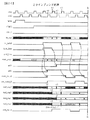
図18及び図19には図16の回路で3ライン加重平均処理を行なう場合のタイミングチャートが示される。図18と図19に示されるタイミングチャートはa−a線で連続する。
【0058】
前記属性情報FILT=1(3ライン加重平均)を伴うブレンド処理コマンドFRECTQがコマンド制御部120で解読されると、先ず、信号CMDがハイレベル(=1)にされ前記セレクタ159がデータパスpe1を選択し、信号FILTがハイレベル(=1)にされ前記セレクタ155、158がデータパスpa1、pd1を選択する。これによってブレンドモジュール132は3ライン加重平均によるブレンド演算処理が可能にされる。
【0059】
画素データin_redはa〜gの順番で入力され、入力データの有効性を示す信号in_validが画素データの入力に同期してハイレベル(=1)にされる。画素データaは、先頭ラインのデータであり、画素データaの入力に同期して信号first_lineがハイレベル(=1)にされ、これに同期して、信号sel1が時刻t0にハイレベル(=1)、信号sel0が時刻t2にハイレベル(=1)にされる。時刻t0にラッチ回路red_reg0にラッチされた画素データaは、時刻t1に同期して2倍回路150で2倍され、2倍された値は、セレクタ156で選択された値“0”及びキャリ(Carry=1)と共に加算される。その加算結果“0+2a+1”は、時刻t1に同期してラッチ回路red_reg3に、時刻t2にラッチ回路red_reg4にラッチされる。一方、時刻t2には初段ラッチ回路red_reg0に次の画素データbがラッチされ、セレクタ157を経由して加算回路154に供給される。ラッチ回路154は前記ラッチ回路red_reg4の出力“0+2a+1”に、画素データb及びキャリ(Carry=1)を加算し、且つ、1/4回路152がその加算結果を下位方向に2ビットのビットシフトを行って、時刻t3に同期して、ラッチ回路red_reg5に、3ライン加重平均された値“(0+2a+b+2)/4を得る。
【0060】
第2ライン目以降に関しては、その直前のラインの画素データが実在しているから、セレクタ156はデータパスpb1を選択することになる。例えば第2ライン目の画素データbが時刻t3に同期して前述と同様に加算回路153で加算されるとき、加算対象とされる直前の画素データaは時刻t2に画素データaをラッチしたラッチ回路red_reg2から与えられ、その加算結果“a+2b+1”が時刻t3にラッチ回路red_reg3にラッチされる。
【0061】
最終ラインの画素データeに関する3ライン加重平均では、その次のラインの画素データは供給されない。したがって、加算回路154はセレクタ157が出力する値“0”を加算対象とする。すなわち、最終ラインの画素データeが時刻t10にラッチ回路red_reg0にラッチされたとき、ラッチ回路red_reg2は直前の画素データdを保持している。画素データeは、2倍回路150及びセレクタ155を通して加算回路153に供給される。加算回路153は“d+2e+1”を演算し、演算結果は時刻t11にラッチ回路red_reg3に、時刻t12にラッチ回路red_reg4にラッチされる。その後、加算回路154は、ラッチ回路red_reg4の値をセレクタ157の出力“0”及びキャリ(carry=1)に加算し、加算結果を1/4して、時刻t13に最終ラインの画素データeに関する3ライン加重平均の値“(d+2e+0)/4”がラッチ回路red_reg5にラッチされる。そして再び、先頭ラインの画素データfから上記同様の演算処理が繰り返される。
【0062】
図20及び図21には図16の回路で2ライン加重平均処理を行なう場合のタイミングチャートが示される。図20と図21に示されるタイミングチャートはb−b線で連続する。
【0063】
前記属性情報FILT=0(2ライン加重平均)を伴うブレンド処理コマンドFRECTQがコマンド制御部120で解読されると、先ず、信号CMDがハイレベル(=1)にされ前記セレクタ159がデータパスpe1を選択し、信号FILTがローレベル(=0)に維持され前記セレクタ155、158がデータパスpa0、pd0を選択する。これによってブレンドモジュール132は2ライン加重平均によるブレンド演算処理が可能にされる。
【0064】
画素データin_redはa〜gの順番で入力され、入力データの有効性を示す信号in_validが画素データの入力に同期してハイレベル(=1)にされる。画素データaは、先頭ラインのデータであり、画素データaの入力に同期して信号first_lineがハイレベル(=1)にされ、これに同期して、信号sel1が時刻t0にハイレベル(=1)、信号sel0が時刻t2にハイレベル(=1)にされる。時刻t0にラッチ回路red_reg0にラッチされた画素データaはセレクタ155を介して加算回路153に供給され、この時セレクタ156は値“0”を選択して加算回路153に与える。加算回路153は、セレクタ155、156の出力をキャリ(Carry=1)と共に加算する。その加算結果“0+a+1”は、1/2回路151で下位方向に1ビットのビットシフトが行われ、時刻t1に同期して、ラッチ回路red_reg5に、2ライン加重平均された値“(0+a+1)/2を得る。
【0065】
第2ライン目以降に関しては、その直前のラインの画素データが実在しているから、セレクタ156はデータパスpb1を選択することになる。例えば第2ライン目の画素データbが時刻t1に同期して前述と同様に加算回路153で加算されるとき、加算対象とされる直前の画素データaは、時刻t2に画素データaをラッチしたラッチ回路red_reg2から与えられ、その加算結果“a+b+1”が得られる。加算結果に対しては1ビットシフト操作が行われ、時刻t3に、その画素データbに関する2ライン加重平均の結果がラッチ回路red_reg5にラッチされる。
【0066】
最終ラインの画素データeに関する2ライン加重平均では、その次のラインの画素データはブレンドモジュール130に供給されない。したがって、加算回路154はセレクタ157が出力する値“0”を加算対象とする。すなわち、最終ラインの画素データeが時刻t10にラッチ回路red_reg0にラッチされたとき、ラッチ回路red_reg2は直前の画素データdを保持している。画素データeは、セレクタ155を通して加算回路153に供給される。加算回路153は“d+e+1”を演算し、演算結果に対する1ビット右シフト操作が1/2回路151で行われ、その演算結果“(d+e+1)/2”がセレクタ158を介して時刻t13にラッチ回路red_reg5にラッチされる。そして再び、先頭ラインの画素データfから上記同様の演算処理が繰り返される。
【0067】
前記ブレンドモジュール130に供給されるソースデータとしての画素データはユニファイドメモリ4から図4に示されるようにワークバッファ101B又はソースバッファ101Cを介して与えられる。このソースデータのアドレスは、ブレンド処理コマンドの前記コマンド引数として与えられるソースアドレスTXS,TYS,TDX,TDY(図9参照)によって決定される。
【0068】
ブレンドモジュール130で加重平均演算された画像データはライトバッファ101Dを介してユニファイドメモリ4のフレームバッファ領域に与えられる。加重平均された画像データの書き込みアドレスは描画アドレス制御部1223で生成され、ライトバッファ101Dを介してユニファイドメモリに供給される。
【0069】
このときの書き込みアドレスは、ブレンド処理コマンドの前記コマンド引数として与えられるディスティネーションアドレスDX1,DY1,DX2,DY2,DX3,DY3,DX4,DY4及び属性情報CLIP(図9参照)によって決定される。
【0070】
例えば、図22に例示されるように、描画座標系にシステムクリッピング領域161が指定され、その中にユーザクリッピング領域163が指定されているとする。それら指定は前記領域指定レジスタ1221A,1221Bの設定値によって決定される。このとき、ブレンド処理コマンドの属性情報CLIP=0のときは、当該コマンドの実行においてユーザクリッピング領域163は無効とされ、ソース画像情報160に対して前記加重平均された画像情報は、ディスティネーションアドレスDX1,DY1,DX2,DY2,DX3,DY3,DX4,DY4で指定される領域162に書き込まれる。
【0071】
一方、ブレンド処理コマンドの属性情報CLIP=1のときは、当該コマンドの実行においてユーザクリッピング領域163は有効され、ソース画像情報160に対して前記加重平均された画像情報は、ディスティネーションアドレスDX1,DY1,DX2,DY2,DX3,DY3,DX4,DY4で指定される領域162とユーザクリッピング領域163とに共通の領域(斜線領域)だけに書き込まれる。
【0072】
このように、ブレンド処理コマンドによるリード・モディファイ・ライトの処理におけるリード及びライトアドレスを、コマンド引数によって任意に指定でき、更に、ユーザクリッピング領域を併用して、そのライト領域を指定することも可能である。したがって、表示領域に対してブレンド処理を施す領域を任意に決定できるという自由度を得ることができる。例えば、自然画とコンピュータ画像とをオーバーレイするとき、コンピュータ画像に対してだけブレンド処理を施す事ができるから、必要な部分の画像情報に対してだけブレンド処理を行なうことができ、無駄な処理を省くことができ、ブレンド処理時間の短縮と画質向上との双方を実現できる。
【0073】
ブレンド処理を経てフレームバッファ領域に格納された画像データがインタレース走査方式で表示されるとき、その1フレーム分の画像データは偶数フィールドと奇数フィールドに分けて前後する別画面として表示される。このとき、表示データはブレンド処理を経ているので、不所望なちらつきは発生しない。
【0074】
以上説明したグラフィックプロセッサ1によれば、描画制御を行なうレンダリングユニット100が隣接する画素データを用いて加重平均を行なうことにより、隣接する走査線間で画像情報の差異が大きい場合にもその差異を緩和する事ができる。このとき、グラフィックプロセッサ1はユニファイドメモリ4から画素データを前記走査方向とは直交する方向に順次読み出して加重平均を行なえばよい。したがって、レンダリングユニット100はもとよりディスプレイユニット102にもラインバッファのような記憶手段を新たに増設することを要しない。したがって、グラフィックプロセッサ1のコストを低減することができる。
【0075】
前記ブレンド処理コマンドは、3ライン加重平均を行なうか2ライン加重平均を行なうかを任意に指定する属性情報FILTを有する。過度な加重平均が行なわれると逆に画像がぼけてしまう虞もあるので、ブレンド処理対象とされるソースデータの特性に応じて加重平均の度合いを前記属性情報FILTで選択でき、これによって、高品質なちらつき防止を実現できる。
【0076】
また、前記ブレンド処理コマンドは、リード・モディファイ・ライトによるリード及びライトアドレスを任意に指定できる上、ユーザクリッピング領域による描画範囲の制限を有効とするか否かを任意に決定する属性情報CLIPを有する。 したがって、表示領域に対してブレンド処理を施す領域を任意に決定できるという自由度を得ることができる。例えば、自然画にコンピュータ画像をオーバーレイなどを考慮したとき、ソース画像の一部をオーバーレイする様な場合に、ソース画像データに対して、加重平均のためのリード・モディファイを行ない、モディファイされた画像データのライトアドレスを任意に指定でき、しかも、クリッピング領域内部だけのオーバレイも選択できる。これにより、フレームバッファ領域の任意の位置に対して、ブレンド処理によるちらつき防止を実現でき、良好な使い勝手を実現することができる。
【0077】
インタネットテレビやナビゲーションシステムなどのデータ処理システムに上記グラフィックプロセッサ1を適用することにより、データ処理システムのコストを低減することができる。
【0078】
以上本発明者によってなされた発明を実施形態に基づいて具体的に説明したが、本発明はそれに限定されるものではなく、その要旨を逸脱しない範囲において種々変更可能であることは言うまでもない。
【0079】
例えば、上記データ処理システムではユニファイドメモリ4を用いたが、例えば図23のように1個のユニファイドメモリ4を第1メモリ170及び第2メモリ171に分け、夫々32ビット、64ビット又は128ビット幅の専用バス172,173を介して描画制御手段2及び表示制御手段3がメモリ170,171を並列的にアクセスできるようにしてもよい。描画制御手段2及び表示制御手段3はバスコントローラ174を介してメモリ170,171の何れに対してもアクセスすることができる。例えば、図24に例示されるように、描画制御手段2と表示制御手段3がメモリ170,171を交互にアクセスしながら、バスネックを解消して描画制御と表示制御を効率化することができる。尚、図23に点線dlで示される部分をも含めて、各回路2,3,170,171,174,172,173を1つの半導体基板(チップ)上に形成されたグラフィックプロセッサ1とすれば、低コスト化及び高性能化を図ることができる。
【0080】
以上の説明では主として本発明者によってなされた発明をその背景となった利用分野であるインタネットテレビやナビゲーションシステムに適用した場合について説明したが、本発明はそれに限定されるものではなく、パーソナルコンピュータやゲーム機など、その他のデータ処理システムに広く適用することができる。
【0081】
【発明の効果】
本願において開示される発明のうち代表的なものによって得られる効果を簡単に説明すれば下記の通りである。
【0082】
すなわち、描画制御手段は、隣接する画素データを用いて加重平均を行なうことにより、隣接する走査線間で画像情報の差異が大きい場合にもその差異を緩和する事ができる。このとき、描画制御手段はメモリから画素データを前記走査方向とは直交する方向に順次読み出して加重平均を行なえばよく、描画制御手段はもとより表示制御手段にもラインバッファのような記憶手段を新たに増設することを要しない。これにより、隣接する走査線の画像情報の差異をラインバッファを増やすことなく緩和することができる。そのようにして、ブレンド処理された画像情報をインタレース走査形式で表示しても、不所望なちらつきは発生しない。
【0083】
ブレンド処理コマンドにおけるソース指定情報とディスティネーション指定情報とを任意に指定できるので、表示領域に対してブレンド処理を施す領域を任意に決定できるという自由度を得ることができる。したがって、必要な部分の画像情報に対してだけブレンド処理を行なうことができ、無駄な処理を省くことができ、ブレンド処理時間の短縮と画質向上との双方を実現できる。
【0084】
ブレンド処理対象とされるソースデータの特性に応じて加重平均の度合いを選択できることにより、過度な加重平均が行なわれることによって逆に画像がぼけてしまう虞を排除でき、高品質なちらつき防止を実現できる。
【0085】
ブレンド処理コマンドによるディスティネーション指定情報に加えて、クリッピング領域も使用してブレンド処理が可能である事により、ブレンド処理の操作性若しくはグラフィックプロセッサの使い勝手を更に向上させることができる。
【図面の簡単な説明】
【図1】本発明の一例に係るグラフィックプロセッサの描画制御手段によるブレンド処理の原理を示す説明図である。
【図2】本発明の一例に係るデータ処理システムのブロック図である。
【図3】グラフィックプロセッサの一例を示すブロック図である。
【図4】レンダリングユニットの一例説明図である。
【図5】レンダリングユニットが実行する描画コマンドの一例を示す説明図である。
【図6】描画コマンドのコマンドコードの一例を示す説明図である。
【図7】描画コマンドの描画属性情報の一例を示す説明図である。
【図8】ブレンド処理コマンドとそのコマンド引数の一例を示す説明図である。
【図9】ブレンド処理コマンドによる処理を模式的に示下説明図である。
【図10】3ラインを加重平均するブレンド演算処理の基本的なアルゴリズムの一例を示す説明図である。
【図11】2ラインを加重平均するブレンド演算処理の基本的なアルゴリズムの一例を示す説明図である。
【図12】ブレンドモジュールの一例を示すブロック図である。
【図13】ブレンドモジュールに含まれる制御部の一例を示すブロック図である。
【図14】制御部による制御の内容を示す状態遷移図である。
【図15】制御部による制御の遷移状態を個々に示す説明図である。
【図16】ブレンドモジュールに含まれる演算部の一例を示すブロック図である。
【図17】ソースデータ、ブレンドモジュール及びフレームバッファの関係の一例を示す説明図である。
【図18】図17のソースデータに対する3ラインブレンド処理の一例を示すタイミングチャートである。
【図19】図18のa−a線に連続する部分を示すタイミングチャートである。
【図20】図17のソースデータに対する2ラインブレンド処理の一例を示すタイミングチャートである。
【図21】図20のb−b線に連続する部分を示すタイミングチャートである。
【図22】ブレンド処理における属性情報CLIPの取り扱いに関する説明図である。
【図23】外部メモリに対するバスネックを解消するための変形例を示すブロック図である。
【図24】図23のメモリ構成を採用したとき描画制御と表示制御のためのメモリアクセス動作態様の一例を示す説明図である。
【符号の説明】
1 グラフィックプロセッサ
2 描画制御手段
3 表示制御手段
4 ユニファイドメモリ
6 CPU
7 メモリ
17 ディスプレイ
100 レンダリングユニット
101 レンダリングバッファユニット
102 ディスプレイユニット
103 ディスプレイバッファユニット
120 コマンド制御部
121 前処理演算部
122 アドレス演算部
123 画素演算部
130 ブレンドモジュール
131 制御部
132 演算部
1221A システムクリッピング領域指定レジスタ
1221B ユーザクリッピング領域指定レジスタ
FRECTQ ブレンド処理コマンド
FILT 第1の属性情報
CLIP 第2の属性情報
160 ソース画像情報
161 システムクリッピング領域
162 加重平均されたソース画像情報
163 ユーザクリッピング領域[0001]
BACKGROUND OF THE INVENTION
The present invention relates to a technique for preventing flicker that may occur when image information intended for display by non-interlaced scanning is displayed by interlaced scanning. For example, the present invention relates to display and drawing control on a computer display. The present invention relates to a graphic processor to be used, and a technique effective when applied to a data processing system using such a graphic processor.
[0002]
[Prior art]
A graphic processor provided in a computer device such as a personal computer supplies image data generated by an application program to the display as a video signal in synchronization with the display timing of the display. In the computer apparatus, the display is controlled by non-interlaced scanning. The non-interlaced scanning method does not perform interlaced scanning of the scanning field, but can scan all scanning lines every time and form one screen in one vertical scanning period, thus obtaining good display quality with little flicker. Can do.
[0003]
On the other hand, the interlaced scanning method adopted in televisions etc. divides the scanning lines into odd and even fields, and scans only one field every vertical scanning period, that is, scans every other scanning line, In this method, one screen is formed in two vertical scanning periods.
[0004]
In the non-interlaced scanning method, all the scanning lines are scanned every vertical scanning period, so the vertical positions of the scanned scanning lines are the same on any screen. However, in the interlaced scanning method, the screen composed of the odd-numbered field scanning lines and the screen composed of the even-numbered field scanning lines are alternately displayed every vertical scanning period. There will be a shift of one scanning line between the successive screens. For this reason, in the interlaced scanning method, if the difference in image information (difference in luminance or color) between adjacent scanning lines is large, flickering easily occurs between the even field screen and the odd field screen.
[0005]
By the way, there is a need to display high-resolution image data created by a personal computer on a normal television set by converting it into a video signal of the NTSC (National Television System Committee) system or the like. However, if the computer image is displayed on the television set as it is simply by changing the scanning method, flickering occurs on the screen, unlike the case of displaying on a non-interlaced scanning method display. This is because a computer image is mainly composed of lines such as characters and shade patterns, and there is a large difference in image information between upper and lower adjacent scanning lines as compared to a natural image by a television, a video camera, or a VTR. For example, when pixels at the same vertical direction on the scanning lines adjacent to each other in the vertical direction have a large difference in luminance such as black, white, and black, the black and white of the pixel portion are displayed on two screens, thereby causing flickering. .
[0006]
Techniques for preventing such flickering are described in JP-A-6-83299, JP-A-7-274086, JP-A-6-46299, and JP-A-8-317311. Each of these techniques has different details, but in each case, a line buffer for storing image information for each scanning line is prepared for each scanning line in the display control system, and an image of the current scanning line is stored in the plurality of line buffers. The image information on the previous scan line is stored together with the information, and the pixel data on the current scan line is corrected using the pixel data at the corresponding position on the previous scan line, so that the difference in image information between the scan lines does not increase. To do.
[0007]
[Problems to be solved by the invention]
Since the line buffer must be operated in synchronization with the display timing, a high-speed SRAM (Static Random Access Memory) or the like must be used for the line buffer. At this time, the prior art requires a plurality of line buffers, which increases the cost of the display control circuit and further the graphic control circuit. Further, the technique for preventing the flickering in the display control system is to perform correction processing when image data that has already been drawn and is stored in the frame buffer is output in synchronization with the display scan. The degree of freedom of performing flicker prevention processing by paying attention to the image or arbitrarily determining the degree of the processing is not considered.
[0008]
An object of the present invention is to provide a graphic processor and a data processing system that can alleviate the difference in image information of adjacent scanning lines without increasing the line buffer.
[0009]
Another object of the present invention is to provide a graphic processor capable of preventing flicker that may occur when image information intended for non-interlaced scanning display is displayed by interlaced scanning without increasing the number of line buffers. And providing a data processing system.
[0010]
Another object of the present invention is to provide a graphic processor and a data processing system capable of freely performing processing for preventing flickering of a screen due to a difference in resolution when image information with different resolutions is overlaid and displayed by interlace scanning. There is to do.
[0011]
It is another object of the present invention to provide a low cost graphic processor having instructions for preventing flicker.
[0012]
Another object of the present invention is to provide a data processing system capable of performing image data processing for preventing flicker in a frame buffer memory.
[0013]
The above and other objects and novel features of the present invention will be apparent from the description of this specification and the accompanying drawings.
[0014]
[Means for Solving the Problems]
The following is a brief description of an outline of typical inventions disclosed in the present application.
[0015]
The graphic processor (1) according to the first aspect of the present invention performs drawing for performing control for drawing pixel data in a memory (4) as a frame buffer in accordance with a command decoding result, as exemplified in FIG. Control means (2) and display control means (3) for controlling the pixel data drawn in the memory in the scanning direction in synchronization with the timing of display scanning. The drawing control means performs a weighted average of pixel data of source image information in which pixel data is arranged corresponding to an arrangement of pixels with pixel data adjacent in a direction orthogonal to the scanning direction, and the source image A blend process for correcting information can be executed. A command (instruction) for performing blend processing is defined for the graphic processor. In the blending process, by performing weighted averaging using adjacent pixel data, even when there is a large difference in image information between adjacent scanning lines, the difference can be reduced. At this time, the drawing control means may read out the pixel data from the memory in the direction orthogonal to the scanning direction and perform weighted averaging, and a new storage means such as a line buffer is added to the display control means as well as the display control means. It is not necessary to add to. Thereby, the difference in image information between adjacent scanning lines can be reduced without increasing the line buffer. In this way, even if the blended image information is displayed in the interlaced scanning format, unwanted flicker does not occur.
[0016]
By providing the graphic processor with an instruction for preventing flickering, a graphic processor capable of preventing flickering at low cost can be provided.
[0017]
A graphic processor according to a second aspect of the present invention comprises a drawing control means for performing control for drawing pixel data in a memory in accordance with a command decoding result, and the pixel data drawn in the memory in synchronization with a display scanning timing. Display control means for performing reading control in the scanning direction, and the drawing control means includes source designation information indicating a location of source image information in which pixel data is arranged corresponding to an arrangement of pixels, and the source designation information. Command information for instructing the pixel data of the source image information to be weighted averaged with the pixel data adjacent in the direction orthogonal to the scanning direction, and the destination designation indicating the location for storing the weighted averaged pixel data The blend processing command having the information can be executed. Thereby, the drawing control unit reads pixel data of the source image information in which pixel data is arranged corresponding to the arrangement of pixels from the memory, and the read pixel data is adjacent in a direction orthogonal to the scanning direction. The blending process can be executed by performing a process such as a read-modify-write process in which a weighted average with other pixel data is written back to the memory. Therefore, it is not necessary to add a storage means such as a line buffer to the display control means as well as the drawing control means, and the difference is alleviated even when there is a large difference in image information between adjacent scanning lines. be able to.
[0018]
Since the source designation information and the destination designation information in the blend processing command can be arbitrarily designated, it is possible to obtain a degree of freedom that an area to be blended can be arbitrarily determined for the display area. For example, when overlaying a natural image and a computer image, a blend process can be performed only on the computer image. Therefore, it is possible to perform the blending process only on the necessary part of the image information, omit unnecessary processing, and realize both shortening of the blending process time and improvement of the image quality.
[0019]
In the blend processing command, the object to be subjected to the weighted average is set as pixel data both before and after adjacent to the direction orthogonal to the scanning direction, or before and after adjacent to the direction orthogonal to the scanning direction. It can have first attribute information that designates whether to use one pixel data. If an excessive weighted average is performed, the image may be blurred, so that the weighted average degree can be selected in accordance with the characteristics of the source data to be blended. This realizes high-quality flicker prevention.
[0020]
The blend processing command further includes second attribute information for instructing to store the weighted average image data only for an area included in a clipping area among areas specified by the destination specification information. Can have. Thereby, in addition to the destination designation information, a clipping region can be used, and the operability of the blending process or the usability of the graphic processor can be further improved.
[0021]
A data processing system according to a third aspect of the present invention includes a central processing unit, a graphic processor, memory means as a frame buffer, and a display. The graphic processor includes: a drawing control unit that performs control for drawing pixel data in the memory unit according to a result of decoding a command issued by the central processing unit; and a display scan of the pixel data drawn in the memory unit by the display. Display control means for performing control to read in the scanning direction in synchronization with the timing and to give to the display. The drawing control means reads pixel data of source image information in which pixel data is arranged corresponding to the arrangement of pixels from the memory means, and reads the read pixel data in other directions adjacent to the direction orthogonal to the scanning direction. It is possible to execute a blending process in which the pixel data is weighted averaged and written back to the memory means. As a result, the graphic processor can execute blend processing by performing processing such as read-modify-write, and can process the image data on the memory means. Therefore, it is not necessary to add a storage means such as a line buffer to the display control means as well as the drawing control means, and the difference is alleviated even when there is a large difference in image information between adjacent scanning lines. be able to.
[0022]
The central processing unit can issue a blend process command to cause the graphic processor to execute the blend process, and the blend process command includes the location of source image information in which pixel data is arranged corresponding to the arrangement of pixels. Source designation information indicating, and pixel information of the source image information indicated by the source designation information, command information for instructing to perform weighted averaging with pixel data adjacent in a direction orthogonal to the scanning direction, and weighted average Destination designation information indicating the location where the pixel data is stored.
[0023]
The blend processing command may further include first attribute information. At this time, the drawing control means, depending on the value of the first attribute information, the target to be weighted average is the pixel data both before and after adjacent in the direction orthogonal to the scanning direction, or It is determined whether the pixel data is one of the pixel data before and after adjacent in the direction orthogonal to the scanning direction. The blend processing command may further include second attribute information. At this time, the drawing control means includes a clipping register in which clipping area designation information is set by the central processing unit, and the second attribute information is designated by the destination designation information in the first state. The weighted averaged image data is stored only for an area included in the clipping area among the areas, and the second attribute information is designated by the destination designation information while ignoring the clipping area in the second state. The weighted averaged image data is stored in the area. As a result, the degree of flicker prevention processing can be arbitrarily determined by paying attention to the characteristics of the source image before drawing, and blend processing can be performed using both the destination designation information and the clipping region. Degree can be achieved.
[0024]
By providing the graphic processor with an instruction for preventing flicker as described above, flicker can be prevented in terms of software. This means that one graphics processor application can be directed to multiple data processing systems.
[0025]
DETAILED DESCRIPTION OF THE INVENTION
<Data processing system>
FIG. 2 shows a block diagram of a data processing system according to an example of the present invention. A CPU (Central Processing Unit) 6 such as a microprocessor or a microcomputer, a
[0026]
When the illustrated data processing system is applied to, for example, a navigation system, the
[0027]
The
[0028]
The
[0029]
The image data output from the
[0030]
《Graphics processor》
FIG. 3 shows an example of the
[0031]
The
[0032]
The
[0033]
The
[0034]
The
The
[0035]
Writing of a command string and texture to the
[0036]
《Rendering unit》
FIG. 4 shows an example of the
[0037]
The
[0038]
The
[0039]
The
[0040]
The
[0041]
The texture
[0042]
The drawing
[0043]
The
[0044]
The pixel calculation performed by the
[0045]
《Blend processing》
FIG. 5 shows a list of drawing commands executed by the
[0046]
FIG. 8 shows an example of the blend process command and its command argument. FIG. 9 schematically shows processing by the blend processing command. The command arguments are TXS, TYS, TDX, TDY, DX1, DY1, DX2, DY2, DX3, DY3, DX4, and DY4. The blend processing command reads and modifies the rectangular source image information specified by TXS, TYS, TDX, TDY, and changes the drawing coordinates specified by DX1, DY1, DX2, DY2, DX3, DY3, DX4, DY4. This is the process of writing. In the modification process, pixel data for each pixel is weighted and averaged with other pixel data adjacent in the vertical direction (direction orthogonal to the scanning direction) to reduce differences in image information (color and luminance) between adjacent scanning lines. Processing (blend calculation processing).
[0047]
10 and 11 show a basic algorithm of the blend calculation process. As shown in FIG. 10, the blend calculation process includes a three-line weighted average for performing a weighted average using pixels corresponding to three adjacent scan lines, and two adjacent scans as shown in FIG. A two-line weighted average that performs a weighted average using pixels corresponding to a line can be performed. Which one is selected is determined by the value of the drawing attribute information FILT. When FILT = 1, 3-line weighted average is performed, and when FILT = 0, 2-line weighted average is performed.
[0048]
As shown in FIG. 10, the three-line weighted average method is applied to pixel data Ci, j in the i-th row in the scanning line direction (lateral direction) and the j-th column in the column direction orthogonal to the scanning line direction. Using pixel data Ci-1, j and Ci + 1, j before and after the column direction, the pixel data Ci-1, j, Ci, j, Ci + 1, j are weighted at a ratio of 1: 2: 1. Add and divide by 4 and average. The division at this time is performed by bit shift (2 bit lower direction (right direction) shift), so that the result of division is rounded off rather than rounded down, and 2 bits are shifted right with respect to a value obtained by adding 2 in advance. An algorithm for performing is used. In the weighted average calculation for the pixel data in the first and last rows, a three-line weighted average is performed using a fixed value of 0.
[0049]
As shown in FIG. 11, the two-line weighted average method uses pixel data Ci-1, j immediately before the column direction for pixel data Ci, j in the i-th row and j-th column, Data Ci-1, j and Ci, j are weighted at a ratio of 1: 1 and added, and then divided by 2 and averaged. An algorithm that shifts 1 bit to the right with respect to a value obtained by adding 1 in advance is employed so that the result of the division at this time is rounded off. In the weighted average calculation for the top pixel data, a fixed value of 0 is used to perform 2-line weighted average.
[0050]
As is apparent from the weighted average calculation algorithm illustrated in FIGS. 10 and 11, when performing weighted averaging, the pixel data is sequentially pixelated in the vertical direction perpendicular to the scanning line direction, such as C0, j to CN, j. Data is read and weighted average is performed, and weighted average pixel data is scanned in the order of reading. Therefore, a line buffer for sequentially storing image information for a plurality of scanning lines in parallel is not required for the weighted average calculation.
[0051]
A block diagram of the
[0052]
The
[0053]
In FIG. 13, the next
[0054]
FIG. 16 shows an example of the
[0055]
In FIG. 16, a double circuit (× 2) 150 is a circuit that gives
[0056]
Next, the operation of the calculation unit in FIG. 16 will be described. In order to facilitate understanding, as shown in FIG. 17, a two-line weighted average and a three-line weighted average for pixels a to g arranged in the vertical direction will be described as an example.
[0057]
FIG. 18 and FIG. 19 show timing charts when the 3-line weighted average processing is performed in the circuit of FIG. The timing charts shown in FIGS. 18 and 19 are continuous along the line aa.
[0058]
When the blend processing command FRECTQ with the attribute information FILT = 1 (3-line weighted average) is decoded by the
[0059]
Pixel data in_red is input in the order of a to g, and a signal in_valid indicating the validity of the input data is set to a high level (= 1) in synchronization with the input of the pixel data. The pixel data a is data of the first line, and the signal first_line is set to a high level (= 1) in synchronization with the input of the pixel data a, and in synchronization with this, the signal sel1 is set to a high level (= 1) at time t0. ), The signal sel0 is set to high level (= 1) at time t2. The pixel data a latched by the latch circuit red_reg0 at time t0 is doubled by the
[0060]
For the second and subsequent lines, the pixel data of the immediately preceding line actually exists, so the
[0061]
In the three-line weighted average for the pixel data e of the last line, the pixel data of the next line is not supplied. Therefore, the
[0062]
20 and 21 show timing charts when the 2-line weighted average processing is performed in the circuit of FIG. The timing charts shown in FIGS. 20 and 21 are continuous along the line bb.
[0063]
When the blend processing command FRECTQ with the attribute information FILT = 0 (2-line weighted average) is decoded by the
[0064]
Pixel data in_red is input in the order of a to g, and a signal in_valid indicating the validity of the input data is set to a high level (= 1) in synchronization with the input of the pixel data. The pixel data a is data of the first line, and the signal first_line is set to a high level (= 1) in synchronization with the input of the pixel data a, and in synchronization with this, the signal sel1 is set to a high level (= 1) at time t0. ), The signal sel0 is set to high level (= 1) at time t2. The pixel data a latched in the latch circuit red_reg0 at time t0 is supplied to the
[0065]
For the second and subsequent lines, the pixel data of the immediately preceding line actually exists, so the
[0066]
In the 2-line weighted average for the pixel data e of the last line, the pixel data of the next line is not supplied to the
[0067]
Pixel data as source data supplied to the
[0068]
The image data subjected to the weighted average calculation by the
[0069]
The write address at this time is determined by the destination addresses DX1, DY1, DX2, DY2, DX3, DY3, DX4, DY4 and attribute information CLIP (see FIG. 9) given as the command arguments of the blend processing command.
[0070]
For example, as illustrated in FIG. 22, it is assumed that a
[0071]
On the other hand, when the attribute information CLIP = 1 of the blend processing command, the
[0072]
In this way, the read and write addresses in the read / modify / write processing by the blend processing command can be arbitrarily specified by the command argument, and the write area can also be specified by using the user clipping area together. is there. Therefore, it is possible to obtain a degree of freedom that an area to be blended with respect to the display area can be arbitrarily determined. For example, when overlaying a natural image and a computer image, blending processing can be performed only on the computer image, so that blending processing can be performed only on the image information of a necessary part, and wasteful processing This can save both blending time and image quality.
[0073]
When the image data stored in the frame buffer area through the blending process is displayed by the interlace scanning method, the image data for one frame is displayed as a separate screen that is divided into an even field and an odd field. At this time, since the display data has undergone the blending process, undesired flicker does not occur.
[0074]
According to the
[0075]
The blend processing command has attribute information FILT for arbitrarily designating whether to perform 3-line weighted average or 2-line weighted average. If an excessive weighted average is performed, the image may be blurred. Therefore, the degree of the weighted average can be selected by the attribute information FILT according to the characteristics of the source data to be blended. Quality flicker prevention can be realized.
[0076]
Further, the blend processing command can arbitrarily specify the read and write addresses by read / modify / write, and has attribute information CLIP that arbitrarily determines whether or not the restriction of the drawing range by the user clipping area is valid. . Therefore, it is possible to obtain a degree of freedom that an area to be blended with respect to the display area can be arbitrarily determined. For example, when a computer image is overlaid on a natural image, when a part of the source image is overlaid, the source image data is read-modified for weighted averaging, and the modified image is displayed. The data write address can be arbitrarily specified, and an overlay only within the clipping area can be selected. As a result, flicker prevention by blending processing can be realized at any position in the frame buffer area, and good usability can be realized.
[0077]
By applying the
[0078]
Although the invention made by the present inventor has been specifically described based on the embodiments, it is needless to say that the present invention is not limited thereto and can be variously modified without departing from the gist thereof.
[0079]
For example, although the
[0080]
In the above description, the case where the invention made mainly by the inventor is applied to the Internet TV and navigation system, which are the fields of use behind the invention, has been described. However, the present invention is not limited thereto, and the personal computer, It can be widely applied to other data processing systems such as game machines.
[0081]
【The invention's effect】
The effects obtained by the representative ones of the inventions disclosed in the present application will be briefly described as follows.
[0082]
That is, the drawing control means can reduce the difference even when there is a large difference in image information between adjacent scanning lines by performing weighted averaging using adjacent pixel data. At this time, the drawing control means may read out the pixel data from the memory in the direction orthogonal to the scanning direction and perform weighted averaging, and a new storage means such as a line buffer is added to the display control means as well as the display control means. It is not necessary to add to. Thereby, the difference in image information between adjacent scanning lines can be reduced without increasing the line buffer. In this way, even if the blended image information is displayed in the interlaced scanning format, unwanted flicker does not occur.
[0083]
Since the source designation information and the destination designation information in the blend processing command can be arbitrarily designated, it is possible to obtain a degree of freedom that an area to be blended can be arbitrarily determined for the display area. Therefore, it is possible to perform the blending process only on the necessary part of the image information, omit unnecessary processing, and realize both shortening of the blending process time and improvement of the image quality.
[0084]
By selecting the degree of weighted average according to the characteristics of the source data to be blended, it is possible to eliminate the possibility that the image will be blurred due to excessive weighted average and to prevent high-quality flicker. it can.
[0085]
In addition to the destination designation information by the blend process command, the blend process can be performed using the clipping region, so that the operability of the blend process or the usability of the graphic processor can be further improved.
[Brief description of the drawings]
FIG. 1 is an explanatory diagram illustrating the principle of blend processing by a drawing control unit of a graphic processor according to an example of the present invention;
FIG. 2 is a block diagram of a data processing system according to an example of the present invention.
FIG. 3 is a block diagram illustrating an example of a graphic processor.
FIG. 4 is an explanatory diagram of an example of a rendering unit.
FIG. 5 is an explanatory diagram illustrating an example of a drawing command executed by a rendering unit.
FIG. 6 is an explanatory diagram illustrating an example of a command code of a drawing command.
FIG. 7 is an explanatory diagram illustrating an example of drawing attribute information of a drawing command.
FIG. 8 is an explanatory diagram showing an example of a blend processing command and its command argument.
FIG. 9 is an explanatory diagram schematically showing processing by a blend processing command.
FIG. 10 is an explanatory diagram showing an example of a basic algorithm of blend calculation processing for weighted averaging of three lines.
FIG. 11 is an explanatory diagram showing an example of a basic algorithm of blend calculation processing for weighted averaging of two lines.
FIG. 12 is a block diagram illustrating an example of a blend module.
FIG. 13 is a block diagram illustrating an example of a control unit included in a blend module.
FIG. 14 is a state transition diagram showing the contents of control by the control unit.
FIG. 15 is an explanatory diagram individually showing transition states of control by the control unit.
FIG. 16 is a block diagram illustrating an example of a calculation unit included in a blend module.
FIG. 17 is an explanatory diagram illustrating an example of a relationship between source data, a blend module, and a frame buffer.
18 is a timing chart showing an example of a three-line blend process for the source data in FIG.
FIG. 19 is a timing chart showing a portion continuing from the aa line in FIG. 18;
20 is a timing chart showing an example of a two-line blend process for the source data of FIG.
FIG. 21 is a timing chart showing a portion continuing from the line bb in FIG. 20;
FIG. 22 is an explanatory diagram regarding handling of attribute information CLIP in blend processing;
FIG. 23 is a block diagram showing a modified example for eliminating a bus neck with respect to an external memory.
24 is an explanatory diagram showing an example of a memory access operation mode for drawing control and display control when the memory configuration of FIG. 23 is adopted.
[Explanation of symbols]
1 Graphics processor
2 Drawing control means
3 Display control means
4 Unified memory
6 CPU
7 memory
17 Display
100 rendering units
101 Rendering buffer unit
102 Display unit
103 Display buffer unit
120 Command control unit
121 Preprocessing operation unit
122 Address calculator
123 Pixel operation unit
130 Blend Module
131 Control unit
132 Calculation unit
1221A System clipping area designation register
1221B User clipping area specification register
FRECQ blend processing command
FILT First attribute information
CLIP second attribute information
160 Source image information
161 System clipping area
162 Weighted average source image information
163 User clipping area
Claims (8)
前記メモリから画素データを表示走査のタイミングに同期して走査方向に読み出す操作を制御する表示制御回路とを有し、
前記ソース画像情報の画素データは、前記メモリに配置されて画素配列に対応する画素データ配列を形成し、前記画素データ配列の列は前記走査方向とは直交され、
前記描画制御回路は前記ブレンド処理を実行可能であり、前記ブレンド処理は、第1の画素データとそれと同一列に配置された前後双方に配置される第2の画素データとを加重平均処理して前記ソース画像情報を補正する第1平均処理と、前記第1の画素データと前記前後何れか一方に配置される第2の画素データとを加重平均処理して前記ソース画像情報を補正する第2平均処理とであり、
前記ブレンド処理コマンドは第1の属性情報を含み、
前記第1の属性情報は、前記第1平均処理と第2平均処理との何れを実行するかを選択的に指定することを特徴とするグラフィックプロセッサ。A drawing control circuit for controlling an operation of storing pixel data of source image information of a rectangular area in a memory according to a decoding result of a plurality of commands including a blend processing command for starting a blend process;
A display control circuit that controls an operation of reading pixel data from the memory in a scanning direction in synchronization with a display scanning timing;
The pixel data of the source image information is arranged in the memory to form a pixel data array corresponding to the pixel array, and the columns of the pixel data array are orthogonal to the scanning direction,
The drawing control circuit can execute the blending process, and the blending process performs a weighted average process on the first pixel data and the second pixel data arranged on both the front and rear sides arranged in the same column as the first pixel data. A first averaging process for correcting the source image information; and a second averaging process for correcting the source image information by performing a weighted averaging process on the first pixel data and the second pixel data arranged on either one of the front and rear sides. With average processing,
The blend processing command includes first attribute information,
The graphic processor according to claim 1, wherein the first attribute information selectively designates which of the first average process and the second average process is executed.
前記メモリから画素データを表示走査のタイミングに同期して走査方向に読み出す操作を制御する表示制御回路とを含み、
前記描画制御回路は、ブレンド処理を実行させるブレンド処理コマンドを実行可能であり、
前記ブレンド処理コマンドは、画素の配列に対応して画素データが配列されたソース画像情報の所在を示すソース指定情報と、前記走査方向と直交する前記画素データ配列と同一列に配置されている互いに隣接配置された画素データの加重平均の計算を要求するコマンド情報と、前記加重平均された画素データを格納する所在を示すディスティネーション指定情報と、を有し、
前記描画制御回路は、第1の画素データとそれと同一列に配置された前後双方に配置される第2の画素データとを加重平均処理して前記ソース画像情報を補正する第1平均処理と、前記第1の画素データと前記前後何れか一方に配置される第2の画素データとを加重平均処理して前記ソース画像情報を補正する第2平均処理とを実行可能であり、
前記ブレンド処理コマンドは更に第1の属性情報を含み、
前記第1の属性情報は、前記第1平均処理と第2平均処理との何れを実行するかを選択的に指定することを特徴とするグラフィックプロセッサ。A drawing control circuit that controls an operation of storing pixel data of source image information of a rectangular area in a memory according to a result of decoding a command;
A display control circuit that controls an operation of reading pixel data from the memory in a scanning direction in synchronization with a display scanning timing;
The drawing control circuit can execute a blend process command for executing a blend process,
The blend processing command includes source designation information indicating the location of source image information in which pixel data is arranged corresponding to the pixel arrangement, and the pixel data arrangement orthogonal to the scanning direction. Command information requesting calculation of a weighted average of adjacently arranged pixel data, and destination designation information indicating a location for storing the weighted average pixel data ,
The drawing control circuit includes a first averaging process that corrects the source image information by performing a weighted average process on the first pixel data and the second pixel data arranged on both the front and rear sides arranged in the same column as the first pixel data; A second averaging process for correcting the source image information by performing a weighted averaging process on the first pixel data and the second pixel data arranged on either one of the front and rear sides;
The blend processing command further includes first attribute information,
The graphic processor according to claim 1, wherein the first attribute information selectively designates which of the first average process and the second average process is executed .
前記メモリから画素データを表示走査のタイミングに同期して走査方向に読み出す操作を制御する表示制御回路とを有し、
前記描画制御回路はブレンド処理コマンドを実行可能であって、
前記ブレンド処理コマンドは、画素の配列に対応して画素データが配列されたソース画像情報の所在を示すソース指定情報と、前記走査方向と直交する前記画素データ配列と同一列に配置され互いに隣接配置された画素データの加重平均の計算を要求するコマンド情報と、前記加重平均された画素データを格納する所在を示すディスティネーション指定情報とを有し、
前記描画制御回路は前記ブレンド処理コマンドに基づいて第1の画素データとそれと同一列に配置された前後双方に配置される第2の画素データとを加重平均処理して前記ソース画像情報を補正する第1平均処理と、前記第1の画素データと前記前後何れか一方に配置される第2の画素データとを加重平均処理して前記ソース画像情報を補正する第2平均処理とを実行可能で、
前記ブレンド処理コマンドは更に第1の属性情報を含み、
前記第1の属性情報は、前記第1平均処理と第2平均処理との何れを実行するかを選択的に指定することを特徴とするグラフィックプロセッサ。A drawing control circuit for controlling an operation of storing pixel data of the source image information in a memory according to a result of decoding the command;
A display control circuit that controls an operation of reading pixel data from the memory in a scanning direction in synchronization with a display scanning timing;
The drawing control circuit can execute a blend processing command,
The blend processing command is arranged adjacent to each other in the same column as the source designation information indicating the location of the source image information in which pixel data is arranged corresponding to the pixel arrangement, and the pixel data arrangement orthogonal to the scanning direction. Command information requesting calculation of a weighted average of the pixel data, and destination designation information indicating a location for storing the weighted average pixel data,
The drawing control circuit corrects the source image information by performing a weighted average process on the first pixel data and the second pixel data arranged on both the front and rear sides arranged in the same column based on the blend processing command. It is possible to execute a first averaging process and a second averaging process that corrects the source image information by performing a weighted averaging process on the first pixel data and the second pixel data arranged in any one of the front and rear sides. ,
The blend processing command further includes first attribute information,
The graphic processor according to claim 1, wherein the first attribute information selectively designates which of the first average process and the second average process is executed .
前記メモリから画素データを表示走査のタイミングに同期して走査方向に読み出す操作を制御する表示制御回路とを有し、
前記描画制御回路はブレンド処理コマンドを実行可能であって、
前記ブレンド処理コマンドは、画素の配列に対応して画素データが配列されたソース画像情報の所在を示すソース指定情報と、前記走査方向とは直交する方向に前記画素データの配列の同じ列上に配置され互いに隣接する画素データの加重平均の計算を要求するコマンド情報と、前記加重平均された画素データを格納する所在を示すディスティネーション指定情報とを有し、
前記ブレンド処理コマンドは更に、前記ディスティネーション指定情報で指定される領域のうちクリッピング領域に含まれる領域に対してだけ前記加重平均された画像データを格納することを指定する属性情報を含むものであり、
前記描画制御回路は、前記ソース画像情報の画素データと共に前記走査方向と直交する列に隣接配置された前後双方に配置される画素データを加重平均処理する第1処理と、前記ソース画像情報の画素データと共に前後何れか一方に配置される画素データを加重平均処理する第2処理とを実行可能であり、
前記ブレンド処理コマンドは更に第1の属性情報を含み、
前記第1の属性情報は、前記第1処理及び第2処理の何れを実行するかを指定することを特徴とするグラフィックプロセッサ。A drawing control circuit that controls an operation of storing pixel data of source image information of a rectangular area in a memory according to a result of decoding a command;
A display control circuit that controls an operation of reading pixel data from the memory in a scanning direction in synchronization with a display scanning timing;
The drawing control circuit can execute a blend processing command,
The blend processing command includes source designation information indicating the location of source image information in which pixel data is arranged corresponding to the pixel arrangement, and the same column of the pixel data arrangement in a direction orthogonal to the scanning direction. Command information that requests calculation of a weighted average of pixel data that are arranged and adjacent to each other, and destination designation information that indicates where to store the weighted averaged pixel data,
The blend processing command further includes attribute information for designating that the weighted averaged image data is stored only for a region included in a clipping region among regions designated by the destination designation information . ,
The drawing control circuit includes a first process for performing a weighted average process on pixel data arranged on both sides of the pixel image of the source image information and adjacent to a column orthogonal to the scanning direction, and pixels of the source image information A second process for performing a weighted average process on pixel data arranged on either the front side or the rear side of the data,
The blend processing command further includes first attribute information,
The graphic processor according to claim 1, wherein the first attribute information specifies which of the first process and the second process is executed .
前記グラフィックプロセッサは、前記中央処理装置により発行されるブレンド処理コマンドを含むコマンドの解読結果に従って画像情報の画素データを前記メモリに格納する操作を制御する描画制御回路と、前記メモリから画素データを前記表示装置の表示走査のタイミングに同期して走査方向に読み出し、前記読み出した画素データを前記表示装置に供給する操作を制御する表示制御回路とを含み、
前記ブレンド処理コマンドは、画素の配列に対応して画素データが配列された画像情報の所在を示すソース指定情報を含み、
前記ソース画像情報の画素データは、前記メモリに配置されて画素配列に対応する画素データ配列を形成し、前記画素データ配列の列は前記走査方向とは直交され、
前記描画制御回路は前記ブレンド処理を実行可能であり、前記ブレンド処理は、前記走査方向と直交する前記画素データ配列と同一列に配置されている互いに隣接配置された画素データの加重平均を行なって前記ソース画像情報を補正する処理であり、
前記描画制御回路は前記メモリに画素データの加重平均結果を格納することができ、
前記中央処理装置は前記ブレンド処理コマンドを実行する前記グラフィックプロセッサにブレンド処理コマンドを出すことができ、
前記ブレンド処理コマンドは、前記走査方向と直交する前記画素データ配列と同一列に配置されている互いに隣接配置された画素データの加重平均の計算を要求するコマンド情報と、前記加重平均された画素データを格納する所在を示すディスティネーション指定情報と、を有し、
前記描画処理回路は、第1の画素データとそれと同一列に配置された前後双方に配置される第2の画素データとを加重平均処理して前記ソース画像情報を補正する第1平均処理と、前記第1の画素データと前記前後何れか一方に配置される第2の画素データとを加重平均処理して前記ソース画像情報を補正する第2平均処理とを実行可能であり、
前記ブレンド処理コマンドは更に第1の属性情報を含み、
前記第1の属性情報は、前記第1平均処理と第2平均処理との何れを実行するかを選択的に指定し、
前記ブレンド処理コマンドは更に、前記ディスティネーション指定情報で指定される領域のうち、クリッピング領域に含まれる領域に対してだけ前記加重平均された画像データを格納することを指定する第2の属性情報を有し、
前記第2の属性情報の第1の状態では前記ディスティネーション指定情報で指定される領域のうちクリッピング領域に含まれる領域に対してだけ前記加重平均された画像データを格納し、
前記第2の属性情報が第2の状態では、前記クリッピング領域を無視し前記ディスティネーション指定情報で指定される領域に前記加重平均された画像データを格納することを特徴とするデータ処理装置。A central processing unit, a graphic processor, a memory, and a display device;
The graphic processor includes a drawing control circuit that controls an operation of storing pixel data of image information in the memory according to a decoding result of a command including a blend processing command issued by the central processing unit, and pixel data from the memory. A display control circuit that controls an operation of reading in the scanning direction in synchronization with a display scanning timing of the display device and supplying the read pixel data to the display device;
The blend processing command includes source designation information indicating the location of image information in which pixel data is arranged corresponding to the arrangement of pixels,
The pixel data of the source image information is arranged in the memory to form a pixel data array corresponding to the pixel array, and the columns of the pixel data array are orthogonal to the scanning direction ,
The drawing control circuit can execute the blending process, and the blending process performs a weighted average of pixel data arranged adjacent to each other arranged in the same column as the pixel data array orthogonal to the scanning direction. A process of correcting the source image information,
The drawing control circuit can store a weighted average result of pixel data in the memory;
The central processing unit can issue a blend processing command to the graphic processor that executes the blend processing command;
The blend processing command includes command information requesting calculation of a weighted average of pixel data arranged adjacent to each other arranged in the same column as the pixel data array orthogonal to the scanning direction, and the weighted averaged pixel data Destination designation information indicating where to store
The drawing processing circuit includes a first averaging process that corrects the source image information by performing a weighted average process on the first pixel data and the second pixel data arranged on both sides of the first pixel data, A second averaging process for correcting the source image information by performing a weighted averaging process on the first pixel data and the second pixel data arranged on either one of the front and rear sides;
The blend processing command further includes first attribute information,
The first attribute information selectively specifies whether to execute the first average process or the second average process,
The blend processing command further includes second attribute information specifying that the weighted average image data is stored only for an area included in a clipping area among areas specified by the destination specification information. Have
In the first state of the second attribute information, the weighted averaged image data is stored only for a region included in a clipping region among regions specified by the destination specification information,
In the second attribute information is a second state, the data processing, wherein the benzalkonium to store the weighted average image data in the area specified by ignoring the clipping region said destination designation information apparatus.
Priority Applications (5)
| Application Number | Priority Date | Filing Date | Title |
|---|---|---|---|
| JP35254397A JP3681528B2 (en) | 1997-12-22 | 1997-12-22 | Graphic processor and data processing system |
| TW087120543A TW428161B (en) | 1997-12-22 | 1998-12-10 | Graphic processor and data processing system |
| US09/213,172 US6384831B1 (en) | 1997-12-22 | 1998-12-17 | Graphic processor and data processing system |
| KR1019980055956A KR19990063179A (en) | 1997-12-22 | 1998-12-18 | Graphic Processor and Data Processing System |
| US09/983,716 US6587111B2 (en) | 1997-12-22 | 2001-10-25 | Graphic processor and data processing system |
Applications Claiming Priority (1)
| Application Number | Priority Date | Filing Date | Title |
|---|---|---|---|
| JP35254397A JP3681528B2 (en) | 1997-12-22 | 1997-12-22 | Graphic processor and data processing system |
Publications (2)
| Publication Number | Publication Date |
|---|---|
| JPH11184454A JPH11184454A (en) | 1999-07-09 |
| JP3681528B2 true JP3681528B2 (en) | 2005-08-10 |
Family
ID=18424786
Family Applications (1)
| Application Number | Title | Priority Date | Filing Date |
|---|---|---|---|
| JP35254397A Expired - Fee Related JP3681528B2 (en) | 1997-12-22 | 1997-12-22 | Graphic processor and data processing system |
Country Status (4)
| Country | Link |
|---|---|
| US (2) | US6384831B1 (en) |
| JP (1) | JP3681528B2 (en) |
| KR (1) | KR19990063179A (en) |
| TW (1) | TW428161B (en) |
Families Citing this family (23)
| Publication number | Priority date | Publication date | Assignee | Title |
|---|---|---|---|---|
| US6636222B1 (en) * | 1999-11-09 | 2003-10-21 | Broadcom Corporation | Video and graphics system with an MPEG video decoder for concurrent multi-row decoding |
| US7982740B2 (en) | 1998-11-09 | 2011-07-19 | Broadcom Corporation | Low resolution graphics mode support using window descriptors |
| US6501480B1 (en) | 1998-11-09 | 2002-12-31 | Broadcom Corporation | Graphics accelerator |
| US6661422B1 (en) * | 1998-11-09 | 2003-12-09 | Broadcom Corporation | Video and graphics system with MPEG specific data transfer commands |
| US6768774B1 (en) | 1998-11-09 | 2004-07-27 | Broadcom Corporation | Video and graphics system with video scaling |
| DE19934208A1 (en) * | 1999-07-21 | 2001-01-25 | Grundig Ag | Method and device for reproducing a line flicker-reduced graphic signal on a television display operating with interlaced display |
| US6954195B2 (en) * | 2000-03-01 | 2005-10-11 | Minolta Co., Ltd. | Liquid crystal display device having a liquid crystal display driven by interlace scanning and/or sequential scanning |
| JP4029253B2 (en) * | 2000-04-10 | 2008-01-09 | 富士フイルム株式会社 | Image resizing apparatus and method |
| US7184059B1 (en) * | 2000-08-23 | 2007-02-27 | Nintendo Co., Ltd. | Graphics system with copy out conversions between embedded frame buffer and main memory |
| JP2002163671A (en) * | 2000-11-27 | 2002-06-07 | Namco Ltd | Game system, program and information storage medium |
| JP2003233366A (en) * | 2002-02-13 | 2003-08-22 | Nec Access Technica Ltd | Display composing circuit and portable electronic equipment |
| KR100450680B1 (en) * | 2002-07-29 | 2004-10-01 | 삼성전자주식회사 | Memory controller for increasing bus bandwidth, data transmitting method and computer system having the same |
| WO2004072934A2 (en) * | 2003-02-11 | 2004-08-26 | Research In Motion Limited | Display processing system and method |
| KR101076900B1 (en) * | 2003-06-12 | 2011-10-25 | 마이크로소프트 코포레이션 | System and method for displaying images utilizing multi-blending |
| US8063916B2 (en) | 2003-10-22 | 2011-11-22 | Broadcom Corporation | Graphics layer reduction for video composition |
| JP2006013701A (en) * | 2004-06-23 | 2006-01-12 | Seiko Epson Corp | Display controller, electronic apparatus, and image data supply method |
| US7695365B2 (en) * | 2004-09-10 | 2010-04-13 | Wms Gaming Inc. | Slot machine with persistent change in symbol function |
| WO2007049449A1 (en) * | 2005-10-26 | 2007-05-03 | Matsushita Electric Industrial Co., Ltd. | Video reproducing device, video recorder, video reproducing method, video recording method, and semiconductor integrated circuit |
| JP4723427B2 (en) * | 2006-06-30 | 2011-07-13 | ルネサスエレクトロニクス株式会社 | Image processing circuit, image processing system, and image processing method |
| ES2621989T3 (en) * | 2009-01-27 | 2017-07-05 | Mitsubishi Electric Corporation | State presentation device and state presentation device presentation method |
| JP5137866B2 (en) * | 2009-01-28 | 2013-02-06 | 三菱電機株式会社 | Equipment operation display device |
| WO2011051756A1 (en) * | 2009-11-02 | 2011-05-05 | Freescale Semiconductor, Inc. | Pixel data processing apparatus and method of processing pixel data |
| US8259120B2 (en) | 2010-06-02 | 2012-09-04 | Dell Products L.P. | Seamless switching between graphics controllers |
Family Cites Families (21)
| Publication number | Priority date | Publication date | Assignee | Title |
|---|---|---|---|---|
| JPH06309425A (en) * | 1990-10-12 | 1994-11-04 | Internatl Business Mach Corp <Ibm> | Equipment and method for graphic display |
| JPH0646299A (en) | 1992-07-27 | 1994-02-18 | Matsushita Electric Ind Co Ltd | Picture display device |
| JPH0683299A (en) | 1992-08-31 | 1994-03-25 | Nec Home Electron Ltd | Scan conversion circuit |
| US5481275A (en) * | 1992-11-02 | 1996-01-02 | The 3Do Company | Resolution enhancement for video display using multi-line interpolation |
| US6130660A (en) * | 1993-10-01 | 2000-10-10 | Maxvision Corporation | System and method for synthesizing high resolution video |
| JPH07274086A (en) | 1994-03-28 | 1995-10-20 | Toshiba Corp | Display controller |
| DE69521741T2 (en) * | 1994-05-03 | 2002-05-23 | Sun Microsystems Inc | Random access memory and system for raster buffers |
| JPH07334669A (en) * | 1994-06-07 | 1995-12-22 | Matsushita Electric Ind Co Ltd | Method and device for graphic processing |
| WO1996007175A1 (en) * | 1994-08-31 | 1996-03-07 | S3 Incorporated | Apparatus for correction of video tearing |
| US6014125A (en) * | 1994-12-08 | 2000-01-11 | Hyundai Electronics America | Image processing apparatus including horizontal and vertical scaling for a computer display |
| US5657047A (en) * | 1995-01-12 | 1997-08-12 | Accelgraphics, Inc. | Method and apparatus for zooming images on a video display |
| JP3075505B2 (en) | 1995-05-10 | 2000-08-14 | インターナショナル・ビジネス・マシーンズ・コーポレ−ション | Display control device and control method thereof |
| WO1997005598A1 (en) * | 1995-07-27 | 1997-02-13 | Magix | Flicker reduction system for computer graphical interlaced display |
| US5936621A (en) * | 1996-06-28 | 1999-08-10 | Innovision Labs | System and method for reducing flicker on a display |
| US5963192A (en) * | 1996-10-11 | 1999-10-05 | Silicon Motion, Inc. | Apparatus and method for flicker reduction and over/underscan |
| US5867180A (en) * | 1997-03-13 | 1999-02-02 | International Business Machines Corporation | Intelligent media memory statically mapped in unified memory architecture |
| US6229521B1 (en) * | 1997-04-10 | 2001-05-08 | Sun Microsystems, Inc. | Method for antialiasing fonts for television display |
| US5963262A (en) * | 1997-06-30 | 1999-10-05 | Cirrus Logic, Inc. | System and method for scaling images and reducing flicker in interlaced television images converted from non-interlaced computer graphics data |
| US6061094A (en) * | 1997-11-12 | 2000-05-09 | U.S. Philips Corporation | Method and apparatus for scaling and reducing flicker with dynamic coefficient weighting |
| US6130723A (en) * | 1998-01-15 | 2000-10-10 | Innovision Corporation | Method and system for improving image quality on an interlaced video display |
| US6034733A (en) * | 1998-07-29 | 2000-03-07 | S3 Incorporated | Timing and control for deinterlacing and enhancement of non-deterministically arriving interlaced video data |
-
1997
- 1997-12-22 JP JP35254397A patent/JP3681528B2/en not_active Expired - Fee Related
-
1998
- 1998-12-10 TW TW087120543A patent/TW428161B/en active
- 1998-12-17 US US09/213,172 patent/US6384831B1/en not_active Expired - Fee Related
- 1998-12-18 KR KR1019980055956A patent/KR19990063179A/en not_active Application Discontinuation
-
2001
- 2001-10-25 US US09/983,716 patent/US6587111B2/en not_active Expired - Lifetime
Also Published As
| Publication number | Publication date |
|---|---|
| TW428161B (en) | 2001-04-01 |
| US6384831B1 (en) | 2002-05-07 |
| KR19990063179A (en) | 1999-07-26 |
| US20020033827A1 (en) | 2002-03-21 |
| US6587111B2 (en) | 2003-07-01 |
| JPH11184454A (en) | 1999-07-09 |
Similar Documents
| Publication | Publication Date | Title |
|---|---|---|
| JP3681528B2 (en) | Graphic processor and data processing system | |
| JP2656737B2 (en) | Data processing device for processing video information | |
| US5270687A (en) | Palette devices, computer graphics systems and method with parallel lookup and input signal splitting | |
| US6191772B1 (en) | Resolution enhancement for video display using multi-line interpolation | |
| US6788309B1 (en) | Method and apparatus for generating a video overlay | |
| JP3818662B2 (en) | Image processing system having a single frame buffer | |
| US5838389A (en) | Apparatus and method for updating a CLUT during horizontal blanking | |
| JPH08202318A (en) | Display control method and its display system for display device having storability | |
| US7796095B2 (en) | Display specific image processing in an integrated circuit | |
| US7307667B1 (en) | Method and apparatus for an integrated high definition television controller | |
| JP3065021B2 (en) | Image mixing processor | |
| WO2005093709A1 (en) | Error accumulation dithering of image data | |
| JPH0432593B2 (en) | ||
| US6232955B1 (en) | Palette devices, systems and methods for true color mode | |
| US5341470A (en) | Computer graphics systems, palette devices and methods for shift clock pulse insertion during blanking | |
| US5815143A (en) | Video picture display device and method for controlling video picture display | |
| JP2010081024A (en) | Device for interpolating image | |
| JPH10116061A (en) | Simultaneously plural image display system and display control method | |
| EP0593012B1 (en) | Video picture display device and method for controlling video picture display | |
| JP3613985B2 (en) | Image processing apparatus and projection display apparatus | |
| EP0465102A2 (en) | Palette devices selection of multiple pixel depths packing the entire width of the bus | |
| JPH0764530A (en) | Control system for image display device | |
| JP3557067B2 (en) | Scanning image generation circuit means | |
| EP0667023A1 (en) | Method and apparatus for updating a clut during horizontal blanking | |
| JP2820068B2 (en) | Image data synthesis display device |
Legal Events
| Date | Code | Title | Description |
|---|---|---|---|
| A521 | Request for written amendment filed |
Free format text: JAPANESE INTERMEDIATE CODE: A523 Effective date: 20040323 |
|
| A621 | Written request for application examination |
Free format text: JAPANESE INTERMEDIATE CODE: A621 Effective date: 20040323 |
|
| A977 | Report on retrieval |
Free format text: JAPANESE INTERMEDIATE CODE: A971007 Effective date: 20040723 |
|
| A131 | Notification of reasons for refusal |
Free format text: JAPANESE INTERMEDIATE CODE: A131 Effective date: 20040803 |
|
| A521 | Request for written amendment filed |
Free format text: JAPANESE INTERMEDIATE CODE: A523 Effective date: 20041001 |
|
| A131 | Notification of reasons for refusal |
Free format text: JAPANESE INTERMEDIATE CODE: A131 Effective date: 20050111 |
|
| A521 | Request for written amendment filed |
Free format text: JAPANESE INTERMEDIATE CODE: A523 Effective date: 20050311 |
|
| TRDD | Decision of grant or rejection written | ||
| A01 | Written decision to grant a patent or to grant a registration (utility model) |
Free format text: JAPANESE INTERMEDIATE CODE: A01 Effective date: 20050510 |
|
| A61 | First payment of annual fees (during grant procedure) |
Free format text: JAPANESE INTERMEDIATE CODE: A61 Effective date: 20050518 |
|
| R150 | Certificate of patent or registration of utility model |
Free format text: JAPANESE INTERMEDIATE CODE: R150 |
|
| FPAY | Renewal fee payment (event date is renewal date of database) |
Free format text: PAYMENT UNTIL: 20080527 Year of fee payment: 3 |
|
| FPAY | Renewal fee payment (event date is renewal date of database) |
Free format text: PAYMENT UNTIL: 20090527 Year of fee payment: 4 |
|
| LAPS | Cancellation because of no payment of annual fees |