JP3678050B2 - Power supply device and electrodeless discharge lamp lighting device - Google Patents
Power supply device and electrodeless discharge lamp lighting device Download PDFInfo
- Publication number
- JP3678050B2 JP3678050B2 JP11730299A JP11730299A JP3678050B2 JP 3678050 B2 JP3678050 B2 JP 3678050B2 JP 11730299 A JP11730299 A JP 11730299A JP 11730299 A JP11730299 A JP 11730299A JP 3678050 B2 JP3678050 B2 JP 3678050B2
- Authority
- JP
- Japan
- Prior art keywords
- circuit
- switching element
- output
- power supply
- short
- Prior art date
- Legal status (The legal status is an assumption and is not a legal conclusion. Google has not performed a legal analysis and makes no representation as to the accuracy of the status listed.)
- Expired - Fee Related
Links
Images


Description
【0001】
【発明の属する技術分野】
本発明は、高周波電力を負荷に供給する電源装置およびこの電源装置を用いて無電極放電灯を点灯させる無電極放電灯点灯装置に関するものである。
【0002】
【従来の技術】
従来から、図6に示すような電源装置が知られている(特開平7−326483号公報参照)。この電源装置は、直流電源Eが電源として供給され、発振回路1aで発生させた高周波をプリアンプ1bで増幅し、プリアンプ1bの出力を出力回路5でさらに増幅して負荷である無電極放電灯20に供給することにより、無電極放電灯20を点灯させるものである。
【0003】
発振回路1aは、水晶振動子XとトランジスタQ2とを用いて高周波を発生するものであり、インダクタL6とコンデンサC15とにより低Qの同調回路を構成した無調整の発振回路である。プリアンプ1bは、トランジスタQ4を用いて発振回路1aの出力をC級増幅するものであり、抵抗R8〜R10は減衰器を構成している。出力回路5は、MOSFETよりなるスイッチング素子Q5によってプリアンプ1bから出力された高周波を増幅する。
【0004】
直流電源Eと出力回路5との間にはフィルタ回路3が挿入され、出力回路5からの高周波が直流電源Eに帰還することを防いでいる。出力回路5と無電極放電灯20との間にはマッチング回路4が挿入され、出力回路5と無電極放電灯20とのインピーダンスマッチングをとり、高周波電力の反射をなくして無電極放電灯20への電力供給の効率をよくしている。
【0005】
無電極放電灯20は、ガラスバルブ内に不活性ガスや金属蒸気などの放電ガスを封入したバルブ7と、バルブ7の外周に近接して巻回された数ターンの空芯コイルよりなる誘導コイル8とによって構成され、誘導コイル8はバルブ7内の放電ガスに高周波電力を供給する。
【0006】
また、図6に示す電源装置では、外部からの出力制御信号に応じてトランジスタQ4のベース・エミッタおよびスイッチング素子Q5のゲート・ソースをそれぞれ短絡させる短絡回路6を調光用に設けている。短絡回路6はMOSFETよりなるスイッチング素子Q3を備え、スイッチング素子Q3のゲート・ソースには外部からの出力制御信号が入力される。スイッチング素子Q3のソースは接地され、ドレインは2個のダイオードD1,D2を介してトランジスタQ4のベースおよびスイッチング素子Q5のゲートにそれぞれ接続される。
【0007】
上述の回路で直流電源Eが供給されると、出力回路5から高周波電力が誘導コイル8に供給され、誘導コイル8には数MHz〜数百MHzの高周波電流が流れる。このとき、誘導コイル8の周囲に生じる高周波電磁界によりバルブ7内の放電ガスが放電して無電極放電灯20が点灯し、バルブ7から紫外線もしくは可視光線が放射される。
【0008】
短絡回路6に入力される出力制御信号には、HレベルまたはLレベルの2値信号が用いられる。短絡回路6への出力制御信号がLレベルである期間には、スイッチング素子Q3はオフ状態であるから、短絡回路6はプリアンプ1bおよび出力回路5に影響を与えず、無電極放電灯20は点灯する。一方、短絡回路6への出力制御信号がHレベルである期間には、スイッチング素子Q3はオン状態となり、トランジスタQ4のベース・エミッタおよびスイッチング素子Q5のゲート・ソースがともに短絡されるので、出力回路5から高周波電力が出力されなくなり、無電極放電灯20は消灯する。
【0009】
上述したように、図6に示す電源装置では、出力制御信号に応じて短絡回路6により出力回路5の出力を制御することができ、無電極放電灯20を点灯・消灯させることができる。ここで、無電極放電灯20を目にチラツキ感を与えない程度の高い繰り返し周期で点滅させ、出力制御信号のHレベルの期間とLレベルの期間との比率を調節すると、無電極放電灯20の光出力を調節することができ、調光制御が可能になる。この種の制御を時分割制御と呼ぶことがある。
【0010】
【発明が解決しようとする課題】
ところで、図7に示すように、出力回路5のスイッチング素子Q5のゲート・ソース間に入力される高周波を適切な振幅に調整するため、あるいは、プリアンプ1bのトランジスタQ4での損失を低減させるために、プリアンプ1bと出力回路5との間に駆動トランスCT1を挿入することが考えられる。この駆動トランスCT1の1次巻線n1はトランジスタQ4のコレクタとエミッタとの間に接続され、2次巻線n2はスイッチング素子Q5のゲート(制御端子)とソースとの間に接続される。
【0011】
図7に示す電源装置では、図6に示した構成と同様に短絡回路6を備える。この回路において短絡回路6のスイッチング素子Q3をオンオフさせたとすると、誘導コイル8の両端電圧は、図8に示すような波形になり、誘導コイル8の両端には無電極放電灯20の始動時(図に示す時刻t)ごとにパルス状の高電圧Pが発生する。このようなパルス状の高電圧Pが発生すると、出力回路5のスイッチング素子Q5にストレスがかかるので、スイッチング素子Q5に耐圧の高い部品が必要となり、場合によってはスイッチング素子Q5が破壊されることがある。
【0012】
パルス状の高電圧Pが発生する原因は、次のように推測される。すなわち、無電極放電灯20の始動時言い換えると短絡回路6のスイッチング素子Q3がオフする瞬間には、トランジスタQ4のベース・エミッタおよびスイッチング素子Q5のゲート・ソースはそれぞれ短絡状態から非短絡状態に移行する。ここで、駆動トランスCT1を介してスイッチング素子Q5を高周波(例えば0.5〜数百MHz)で動作させると、プリアンプ1bから出力回路5までの配線容量や駆動トランスCT1の各巻線の両端間における浮遊容量などの影響により、パルス状の高電圧Pが発生すると推測される。
【0013】
本発明は上記事由に鑑みてなされたものであり、その目的は、電源投入時や外部からの出力制御信号に応じて出力回路の出力電力を制御する際における出力回路のスイッチング素子の破壊を防止した電源装置およびこの電源装置を用いて無電極放電灯を点灯させる無電極放電灯点灯装置を提供することにある。
【0014】
【課題を解決するための手段】
請求項1の発明は、高周波を発生する高周波発生回路と、第1のスイッチング素子を用いて負荷に高周波電力を出力する出力回路と、上記高周波発生回路の出力が1次巻線に供給され上記第1のスイッチング素子の制御端子が2次巻線に接続された駆動トランスと、上記駆動トランスの1次巻線の両端間を短絡させるとともに上記第1のスイッチング素子の制御端子を接地する状態を短絡状態として選択可能とする短絡回路とを備えた電源装置である。この構成によれば、短絡回路によって駆動トランスの1次巻線の両端間を短絡させるとともに出力回路の第1のスイッチング素子の制御端子を接地することにより、高周波発生回路から出力回路までの配線容量や駆動トランスの各巻線の両端間における浮遊容量などの影響が小さくなるので、出力回路の始動時において負荷の両端に高電圧のパルス状の高電圧が発生することがなく、第1のスイッチング素子にかかるストレスを低減させて第1のスイッチング素子の破壊を防止することができる。
【0015】
請求項2の発明は、請求項1の発明において、上記高周波発生回路は出力端間に接続された第2のスイッチング素子を含み、上記短絡回路は、短絡状態として上記第2のスイッチング素子の制御端子を接地する状態を含んでいるものである。この構成によれば、短絡回路が高周波発生回路の第2のスイッチング素子の制御端子を接地することにより、高周波発生回路における配線容量などの影響も小さくなるので、請求項1の発明よりも確実にパルス状の高電圧の発生を防止することができる。
【0016】
請求項3の発明は、請求項2の発明において、上記高周波発生回路はインダクタおよびコンデンサよりなる共振回路を有し、上記コンデンサは上記第2のスイッチング素子と並列接続されるとともに上記第2のスイッチング素子の近傍に配置されているものである。この構成によれば、共振回路のコンデンサが高周波発生回路の第2のスイッチング素子と並列接続されるとともに第2のスイッチング素子の近傍に配置されているから、第2のスイッチング素子と上記コンデンサとの間の配線におけるインダクタンスが小さくなり、第2のスイッチング素子における波形歪みが小さくなるので、請求項2の発明よりもさらにパルス状の高電圧の発生を防止することができる。
【0017】
請求項4の発明は、請求項1または請求項2の発明において、上記短絡回路は、少なくとも電源投入直後からあらかじめ設定された期間に短絡状態を選択するものである。この構成によれば、電源投入直後からあらかじめ設定された期間は短絡回路が駆動トランスの1次巻線の両端間を短絡するとともに出力回路の第1のスイッチング素子の制御端子を接地するので、電源投入直後に電源電圧が安定した後に出力回路の動作を開始させることができる。
【0018】
請求項5の発明は、請求項1ないし請求項3の発明において、上記短絡回路は、外部からの出力制御信号に応じて短絡状態の選択・非選択を繰り返すとともにその比率が制御されることにより、上記出力回路の出力電力を制御するものである。この構成によれば、出力制御信号を用いて出力電力を調節することができる。
【0019】
請求項6の発明は、請求項1ないし請求項5の発明において、上記出力回路の出力周波数は0.5〜数百MHzに設定されているものである。
【0020】
請求項7の発明は、請求項1ないし請求項6の発明において、上記高周波発生回路と上記駆動トランスの1次巻線との間に両者のインピーダンスを整合させるマッチング回路を設けたものである。この構成によれば、マッチング回路によって高周波発生回路と駆動トランスの1次巻線との間のインピーダンスを整合させることができるので、高周波発生回路で発生した高周波を効率よく駆動トランスに伝達することができる。
【0021】
請求項8の発明は、請求項1ないし請求項7の発明において、上記高周波発生回路は、水晶振動子を含む発振回路を有するものである。この構成によれば、水晶振動子によって、高周波発生回路の出力周波数を設定することができるとともに、高周波発生回路の出力周波数を安定させることができる。
【0022】
請求項9の発明は、請求項1ないし請求項7の発明において、上記高周波発生回路は、上記出力回路で生じる振動電流の一部を上記駆動トランスの1次巻線に流すように帰還するものである。この構成によれば、高周波発生回路が出力回路で生じる振動電流の一部を駆動トランスの1次巻線に流すように帰還することにより、第1のスイッチング素子が自励駆動され、第1のスイッチング素子を他励駆動させる構成よりも部品点数が少なくなり回路構成が簡単になる。
【0023】
請求項10の発明は、請求項1ないし請求項9の発明において、上記短絡回路は、一端が接地された第3のスイッチング素子の他端に一端が共通接続された複数個のダイオードを有し、上記複数個のダイオードには、上記第1のスイッチング素子の制御端子に他端が接続された第1のダイオードと、上記駆動トランスの1次巻線に他端が接続された第2のダイオードとが含まれているものである。この構成によれば、短絡回路の第3のスイッチング素子の他端に複数個のダイオードの一端が共通接続されているから、第3のスイッチング素子によって複数個のダイオードの他端が接続された複数箇所を同時に短絡させることができ、複数箇所を短絡させるために複数個のスイッチング素子を設ける必要がない。
【0024】
請求項11の発明は、請求項10の発明において、上記第3のスイッチング素子と上記第1のダイオードとの直列回路は、上記第1のスイッチング素子の制御端子の近傍に配置されているものである。この構成によれば、短絡回路の第3のスイッチング素子と第1のダイオードとの直列回路が出力回路の第1のスイッチング素子の近傍に配置されているから、第3のスイッチング素子から第1のダイオードを介した第1のスイッチング素子までの配線容量が小さくなり、第1のスイッチング素子における波形歪みが小さくなるので、これによってもパルス状の高電圧の発生を抑制することができる。
【0025】
請求項12の発明は、請求項1ないし請求項11のいずれかに記載の電源装置と、上記電源装置からの高周波電力により点灯する上記負荷としての無電極放電灯とを備えた無電極放電灯点灯装置である。
【0026】
請求項13の発明は、水晶振動子を含む発振回路を有し0.5〜数百MHzの高周波を発生する高周波発生回路と、第1のスイッチング素子を用いて高周波電力を出力する出力回路と、上記高周波発生回路の出力が1次巻線に供給され上記第1のスイッチング素子の制御端子が2次巻線に接続された駆動トランスと、上記出力回路からの高周波電力により点灯される無電極放電灯と、一端が接地された第2のスイッチング素子の他端に一端が共通接続され他端が上記駆動トランスの1次巻線および上記第1のスイッチング素子の制御端子にそれぞれ接続された2個のダイオードを有する短絡回路とを備え、上記短絡回路は、上記駆動トランスの1次巻線の両端間を短絡させるとともに上記第1のスイッチング素子の制御端子を接地する状態を選択可能とされている無電極放電灯点灯装置である。
【0027】
【発明の実施の形態】
以下、本発明の実施の形態を図面に基づいて説明する。
【0028】
(実施形態1)
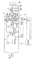
本実施形態は、図1に示すように、図7に示した電源装置において、プリアンプ1bのトランジスタQ4のベースに接続したダイオードD1に代えて、駆動トランスCT1の1次巻線n1とスイッチング素子Q3のドレインとの接続点にダイオードD3のアノードを接続したものである。
【0029】
本実施形態では、発振回路1aとプリアンプ1bとにより高周波発生回路1を構成している。また、直流電源Eが投入されてからあらかじめ設定された期間は出力回路5を始動させないためにタイマ回路9を設けている。他の構成は図7に示した従来構成と同様である。
【0030】
タイマ回路9は、抵抗R50,R51の直列回路、抵抗R52,R53の直列回路、コンデンサC50、コンパレータIC1により構成され、抵抗R50,R51の直列回路と抵抗R52,R53の直列回路とは直流電源Eにそれぞれ並列接続される。抵抗R50,R51の接続点にはコンパレータIC1の非反転入力端が接続され、抵抗R52,R53の接続点にはコンパレータIC1の反転入力端が接続され、抵抗R53の両端間にはコンデンサC50が接続される。コンパレータIC1の出力端は、短絡回路6を構成するスイッチング素子Q3のゲートに接続される。
【0031】
タイマ回路9では、直流電源Eが投入されると、抵抗R52を介してコンデンサC50の充電が始まり、コンデンサC50の両端電圧が抵抗R51の両端電圧よりも低い期間には、コンパレータIC1の出力はHレベルとなる。その後、コンデンサC50が充電されて、コンデンサC50の両端電圧が抵抗R51の両端電圧よりも高くなると、コンパレータIC1の出力はLレベルとなる。したがって、コンパレータIC1の出力は、電源投入から一定時間はHレベルであって、その後Lレベルに移行する。
【0032】
次に、本実施形態の電源装置の動作について説明する。図2(b)に示すように、時刻t0において直流電源Eが投入されると、上述したようにタイマ回路9の出力はHレベルとなる。このとき、短絡回路6のスイッチング素子Q3がオンし、駆動トランスCT1の1次巻線n1の両端間およびスイッチング素子Q5のゲート・ソースがともに短絡されるから、スイッチング素子Q5はオフする。その結果、出力回路5から無電極放電灯20の誘導コイル8に高周波電力が供給されず、無電極放電灯20は消灯した状態に保たれる。ここに、スイッチング素子Q3がオンになったときの状態を短絡状態と呼ぶことにする。
【0033】
その後、タイマ回路9により設定された時間が経過して時刻t1になると、タイマ回路9の出力はLレベルとなる。このとき、スイッチング素子Q3がオフし、駆動トランスCT1の1次巻線n1の両端間およびスイッチング素子Q5のゲート・ソースはともに短絡されなくなるから、スイッチング素子Q5は動作を開始する。こうして、出力回路5から誘導コイル8に高周波電力が供給され、無電極放電灯20は点灯する。
【0034】
上述した動作によって、誘導コイル8の両端電圧は、図2(a)に示す波形になる。つまり、出力回路5の始動時(時刻t1)において、図8に示したパルス状の高電圧Pは発生しなくなる。その結果、出力回路5のスイッチング素子Q5にかかるストレスを低減させてスイッチング素子Q5の破壊を防止することができる。
【0035】
また、直流電源Eの投入直後からタイマ回路9により設定された期間は、短絡回路6が短絡状態であって出力回路5の動作が停止しているから、直流電源Eの投入直後にスイッチング素子Q5に過大な電流が流れることがなく、しかも誘導コイル8には通電開始時から大きい電流を流すことができ、無電極放電灯20が始動しやすくなる。
【0036】
(実施形態2)
本実施形態は、図3に示すように、プリアンプ1bがMOSFETよりなるスイッチング素子Q53を備え、このスイッチング素子Q53のゲート・ソースも短絡回路6により短絡状態が選択可能になっているものである。また、出力回路5にMOSFETよりなる2個のスイッチング素子Q51,Q52を用い、各スイッチング素子Q51,Q52が交互にオンオフすることによって高周波電力を出力する構成を採用している。さらに、出力回路5が2個のスイッチング素子Q51,Q52を備えるから、1次巻線n21と2個の2次巻線n22,n23とを備える駆動トランスCT2を用いている。また、本実施形態では、商用電源ACを直流電源回路E1により直流に変換して直流電源を得ている。
【0037】
プリアンプ1bは、スイッチング素子Q53と、インダクタL51とコンデンサC51との直列回路よりなる共振回路とによって構成され、発振回路1aから出力された高周波をスイッチング素子Q53により増幅して駆動トランスCT2の1次巻線n21に出力する。コンデンサC51はスイッチング素子Q53に並列接続されるとともに、スイッチング素子Q53の近傍に配置されている。
【0038】
プリアンプ1bと駆動トランスCT2の1次巻線n21との間には、2個のコンデンサC52,C53により構成されたマッチング回路10が挿入され、プリアンプ1bと駆動トランスCT2の1次巻線n21との間のインピーダンスを整合させている。
【0039】
出力回路5は、スイッチング素子Q51,Q52の直列回路と、インダクタLsとコンデンサCsとの直列回路よりなる共振回路とによって構成される。スイッチング素子Q51,Q52の直列回路の両端には直流電源回路E1の出力端が接続される。各スイッチング素子Q51,Q52のゲートとソースとの間には駆動トランスCT2の2次巻線n22,n23と抵抗R61,R62との並列回路がそれぞれ接続され、スイッチング素子Q52のドレインとソースとの間にはインダクタLsとコンデンサCsとからなる共振回路およびマッチング回路4を介して無電極放電灯20の誘導コイル8が接続される。マッチング回路4は、3個のコンデンサC30〜C32を用いて構成され、出力回路5と誘導コイル8との間のインピーダンスを整合させている。
【0040】
プリアンプ1bの出力は駆動トランスCT2を介して出力回路5の各スイッチング素子Q51,Q52を交互にオンオフさせる。つまり、プリアンプ1bから出力された高周波は出力回路5でD級増幅されて、誘導コイル8に供給される。
【0041】
短絡回路6は、カソードがスイッチング素子Q3に共通接続された3個のダイオードD2,D3,D4を備える。各ダイオードD2,D3,D4のアノードは、スイッチング素子Q52のゲート、駆動トランスCT2の1次巻線n21の一端、スイッチング素子Q53のゲートにそれぞれ接続される。
【0042】
次に、本実施形態の動作について説明する。商用電源ACが投入されると直流電源回路E1から直流電力が供給され、実施形態1と同様にタイマ回路9の出力がHレベルとなる。このとき、スイッチング素子Q3がオンし、駆動トランスCT2の1次巻線n21の両端間および各スイッチング素子Q52,Q53のゲート・ソースがともに短絡されるので、スイッチング素子Q53はオフを保持してプリアンプ1bでの増幅が行われず、スイッチング素子Q51,Q52もオフに保たれる。その結果、出力回路5から誘導コイル8に高周波電力が供給されず、無電極放電灯20は点灯しない。以後の動作は実施形態1と同様である。
【0043】
本実施形態では、短絡回路6によって、駆動トランスCT2の1次巻線n21の両端間および出力回路5のスイッチング素子Q52のゲート・ソースだけでなく、高周波発生回路1(プリアンプ1b)のスイッチング素子Q53のゲート・ソースも短絡させることにより、高周波発生回路1における配線容量などの影響も小さくなるので、実施形態1よりも確実にパルス状の高電圧Pの発生を防止することができる。
【0044】
また、高周波発生回路1のスイッチング素子Q53の近傍に第1の共振回路のコンデンサC51を配置することにより、スイッチング素子Q53とコンデンサC51との間の配線におけるインダクタンスが小さくなり、スイッチング素子Q53における波形歪みが小さくなるので、これによってもパルス状の高電圧Pの発生を抑制することができる。
【0045】
さらにまた、高周波発生回路1と駆動トランスCT2の1次巻線n21との間にマッチング回路10を挿入していることにより、高周波発生回路1と駆動トランスCT2の1次巻線n21とのインピーダンスが整合するので、高周波発生回路1で発生した高周波を効率よく駆動トランスCT2に伝達することができる。
【0046】
(実施形態3)
本実施形態は、図4に示すように、実施形態2の構成において、タイマ回路9に代えて、短絡回路6に2値信号である出力制御信号を与える制御回路11を外部回路として設けたものである。
【0047】
本実施形態では、制御回路11からの出力制御信号によって、短絡回路6で出力回路5から無電極放電灯20に与える出力電力を制御することができる。つまり、目にチラツキ感を与えない程度の高い繰り返し周期で無電極放電灯20を点滅させ、制御回路11で出力制御信号のデューティー比を変化させると、無電極放電灯20の明るさを変化させる調光制御を行うことができる。
【0048】
本実施形態では、無電極放電灯20の調光制御を行う際に、出力回路5の動作開始と動作停止とを繰り返しているが、動作開始前まで短絡回路6によって駆動トランスCT2の1次巻線n21の両端間および各スイッチング素子Q52,Q53のゲート・ソースがともに短絡されているので、無電極放電灯20の誘導コイル8の両端にパルス状の高電圧Pが発生することがない。
【0049】
(実施形態4)
本実施形態は、図5に示すように、出力回路5としてMOSFETよりなる2個のスイッチング素子Q54,Q55の直列回路とインダクタLsとコンデンサCsとの直列回路よりなる共振回路とによって構成したものを用い、スイッチング素子Q54,Q55を自励駆動するようにしたものである。したがって、出力回路5で発生する高周波電力の一部を帰還する回路を高周波発生回路1として用いている。この高周波電力は、1次巻線n31と2個の2次巻線n32,n33とを備えた駆動トランスCT3を介してスイッチング素子Q54,Q55の駆動に用いられる。
【0050】
スイッチング素子Q54,Q55の直列回路の両端には直流電源回路E1の出力端が接続される。スイッチング素子Q55のドレインとソースとの間には上記共振回路を介して無電極放電灯20の誘導コイル8が接続される。駆動トランスCT3の1次巻線n31、コンデンサC54、上記共振回路、誘導コイル8により閉回路が構成され、駆動トランスCT3の各2次巻線n32,n33には各スイッチング素子Q54,Q55のゲート・ソースがそれぞれ接続される。
【0051】
本実施形態では、電源投入直後に出力回路5に起動パルスを与える起動回路12を設けてある。この起動パルスはスイッチング素子Q55のゲート・ソースに与えられる。スイッチング素子Q54のドレインとソースとの間には抵抗R60が接続され、出力回路5を起動しやすくしている。
【0052】
また、実施形態3と同様に制御回路11および短絡回路6を設けており、短絡回路6はスイッチング素子Q3のドレインにカソードを共通接続した2個のダイオードD5,D6を備える。各ダイオードD5,D6のアノードは、駆動トランスCT3の1次巻線n31とスイッチング素子Q55のゲートとにそれぞれ接続される。
【0053】
次に、本実施形態の電源装置の動作について説明する。商用電源ACが投入されると、直流電源回路E1から直流電力が供給される。そして、起動回路12からスイッチング素子Q55のゲート・ソースに起動パルスが与えられてスイッチング素子Q55がオンし、上記共振回路の共振作用によって振動電流が発生する。この振動電流がコンデンサC54を介して駆動トランスCT3の1次巻線n31に流れることにより、駆動トランスCT3の各2次巻線n32,n33から各スイッチング素子Q54,Q55のゲート・ソースにそれぞれ高周波が与えられ、スイッチング素子Q54,Q55は交互にオンオフされる。その結果、スイッチング素子Q55のドレイン・ソースから上記共振回路を介して誘導コイル8に高周波電力が供給され、無電極放電灯20が点灯する。すなわち、上記共振回路から発生した振動電流を駆動トランスCT3の1次巻線n31に流すことにより、スイッチング素子Q54,Q55は自励駆動される。
【0054】
本実施形態では、無電極放電灯20の調光制御を行う際に、短絡回路6によって駆動トランスCT3の1次巻線n31の両端間およびスイッチング素子Q55のゲート・ソースがともに短絡されるので、出力回路5bのスイッチング素子Q54,Q55を自励駆動しながらも、無電極放電灯20の誘導コイル8の両端にパルス状の高電圧Pが発生することがなく、スイッチング素子Q54,Q55の破壊を防止することができる。他の構成および動作は実施形態3と同様である。
【0055】
なお、上述した各実施形態では、タイマ回路9を用いて電源投入直後からあらかじめ設定された期間は出力回路を始動させないようにする例と、制御回路11を用いて無電極放電灯20の調光制御を行う例とを示したが、無負荷時などに何らかの異常を検出して出力回路の出力を断続させる回路にも本発明の技術思想は適用可能である。つまり、駆動トランスの1次巻線の両端間を短絡させるとともに出力回路のスイッチング素子の制御端子を接地するという動作を行うか否かによって出力回路の出力を制御するものであれば、どのようなものにも適用することができる。
【0056】
【発明の効果】
請求項1の発明は、高周波を発生する高周波発生回路と、第1のスイッチング素子を用いて負荷に高周波電力を出力する出力回路と、上記高周波発生回路の出力が1次巻線に供給され上記第1のスイッチング素子の制御端子が2次巻線に接続された駆動トランスと、上記駆動トランスの1次巻線の両端間を短絡させるとともに上記第1のスイッチング素子の制御端子を接地する状態を短絡状態として選択可能とする短絡回路とを備えた電源装置であり、短絡回路によって駆動トランスの1次巻線の両端間を短絡させるとともに出力回路の第1のスイッチング素子の制御端子を接地することにより、高周波発生回路から出力回路までの配線容量や駆動トランスの各巻線の両端間における浮遊容量などの影響が小さくなるので、出力回路の始動時において負荷の両端に高電圧のパルス状の高電圧が発生することがなく、第1のスイッチング素子にかかるストレスを低減させて第1のスイッチング素子の破壊を防止することができるという効果がある。
【0057】
請求項2の発明は、請求項1の発明において、上記高周波発生回路は出力端間に接続された第2のスイッチング素子を含み、上記短絡回路は、短絡状態として上記第2のスイッチング素子の制御端子を接地する状態を含んでいるものであり、短絡回路が高周波発生回路の第2のスイッチング素子の制御端子を接地することにより、高周波発生回路における配線容量などの影響も小さくなるので、請求項1の発明よりも確実にパルス状の高電圧の発生を防止することができるという効果がある。
【0058】
請求項3の発明は、請求項2の発明において、上記高周波発生回路はインダクタおよびコンデンサよりなる共振回路を有し、上記コンデンサは上記第2のスイッチング素子と並列接続されるとともに上記第2のスイッチング素子の近傍に配置されているから、第2のスイッチング素子と上記コンデンサとの間の配線におけるインダクタンスが小さくなり、第2のスイッチング素子における波形歪みが小さくなるので、請求項2の発明よりもさらにパルス状の高電圧の発生を防止することができるという効果がある。
【0059】
請求項4の発明は、請求項1または請求項2の発明において、上記短絡回路は、少なくとも電源投入直後からあらかじめ設定された期間に短絡状態を選択するものであり、電源投入直後からあらかじめ設定された期間は短絡回路が駆動トランスの1次巻線の両端間を短絡するとともに出力回路の第1のスイッチング素子の制御端子を接地するので、電源投入直後に電源電圧が安定した後に出力回路の動作を開始させることができるという利点がある。
【0060】
請求項5の発明は、請求項1ないし請求項3の発明において、上記短絡回路は、外部からの出力制御信号に応じて短絡状態の選択・非選択を繰り返すとともにその比率が制御されることにより、上記出力回路の出力電力を制御するものであり、出力制御信号を用いて出力電力を調節することができるという利点がある。
【0061】
請求項7の発明は、請求項1ないし請求項6の発明において、上記高周波発生回路と上記駆動トランスの1次巻線との間に両者のインピーダンスを整合させるマッチング回路を設けたものであり、マッチング回路によって高周波発生回路と駆動トランスの1次巻線との間のインピーダンスを整合させることができるので、高周波発生回路で発生した高周波を効率よく駆動トランスに伝達することができるという利点がある。
【0062】
請求項8の発明は、請求項1ないし請求項7の発明において、上記高周波発生回路は、水晶振動子を含む発振回路を有するものであり、水晶振動子によって、高周波発生回路の出力周波数を設定することができるとともに、高周波発生回路の出力周波数を安定させることができるという利点がある。
【0063】
請求項9の発明は、請求項1ないし請求項7の発明において、上記高周波発生回路は、上記出力回路で生じる振動電流の一部を上記駆動トランスの1次巻線に流すように帰還するから、第1のスイッチング素子が自励駆動され、第1のスイッチング素子を他励駆動させる構成よりも部品点数が少なくなり回路構成が簡単になるという利点がある。
【0064】
請求項10の発明は、請求項1ないし請求項9の発明において、上記短絡回路は、一端が接地された第3のスイッチング素子の他端に一端が共通接続された複数個のダイオードを有し、上記複数個のダイオードには、上記第1のスイッチング素子の制御端子に他端が接続された第1のダイオードと、上記駆動トランスの1次巻線に他端が接続された第2のダイオードとが含まれているものであり、短絡回路の第3のスイッチング素子の他端に複数個のダイオードの一端が共通接続されているから、第3のスイッチング素子によって複数個のダイオードの他端が接続された複数箇所を同時に短絡させることができ、複数箇所を短絡させるために複数個のスイッチング素子を設ける必要がないという利点がある。
【0065】
請求項11の発明は、請求項10の発明において、上記第3のスイッチング素子と上記第1のダイオードとの直列回路は、上記第1のスイッチング素子の制御端子の近傍に配置されているから、第3のスイッチング素子から第1のダイオードを介した第1のスイッチング素子までの配線容量が小さくなり、第1のスイッチング素子における波形歪みが小さくなるので、これによってもパルス状の高電圧の発生を抑制することができるという利点がある。
【図面の簡単な説明】
【図1】本発明の実施形態1の回路図である。
【図2】同上の動作波形図である。
【図3】本発明の実施形態2の回路図である。
【図4】本発明の実施形態3の回路図である。
【図5】本発明の実施形態4の回路図である。
【図6】従来例の回路図である。
【図7】別の従来例の回路図である。
【図8】同上の動作波形図である。
【符号の説明】
1 高周波発生回路
1a 発振回路
5 出力回路
6 短絡回路
10 マッチング回路
20 無電極放電灯
C51 コンデンサ
CT1〜CT3 駆動トランス
D2〜D6 ダイオード
L51 インダクタ
n1,n21,n31 1次巻線
Q3,Q5 スイッチング素子
Q51〜Q55 スイッチング素子
X 水晶振動子[0001]
BACKGROUND OF THE INVENTION
The present invention relates to a power supply device that supplies high-frequency power to a load and an electrodeless discharge lamp lighting device that lights an electrodeless discharge lamp using the power supply device.
[0002]
[Prior art]
Conventionally, a power supply device as shown in FIG. 6 is known (see Japanese Patent Application Laid-Open No. 7-326483). In this power supply apparatus, a DC power source E is supplied as a power source, the high frequency generated by the
[0003]
The
[0004]
A
[0005]
The
[0006]
Further, in the power supply device shown in FIG. 6, a
[0007]
When the DC power source E is supplied in the above-described circuit, high frequency power is supplied from the
[0008]
As an output control signal input to the
[0009]
As described above, in the power supply device shown in FIG. 6, the output of the
[0010]
[Problems to be solved by the invention]
Incidentally, as shown in FIG. 7, in order to adjust the high frequency input between the gate and source of the switching element Q5 of the
[0011]
The power supply device shown in FIG. 7 includes the
[0012]
The cause of the generation of the pulsed high voltage P is estimated as follows. That is, when the
[0013]
The present invention has been made in view of the above reasons, and its purpose is to prevent the switching elements of the output circuit from being destroyed when the power is turned on or when the output power of the output circuit is controlled in accordance with an external output control signal. Another object is to provide an electrodeless discharge lamp lighting device that lights an electrodeless discharge lamp using the power supply device.
[0014]
[Means for Solving the Problems]
According to the first aspect of the present invention, there is provided a high frequency generation circuit for generating a high frequency, an output circuit for outputting high frequency power to a load using a first switching element, and an output of the high frequency generation circuit being supplied to a primary winding. A state in which the control terminal of the first switching element is short-circuited between both ends of the drive transformer connected to the secondary winding and the primary winding of the drive transformer and the control terminal of the first switching element is grounded The power supply device includes a short circuit that can be selected as a short circuit state. According to this configuration, both ends of the primary winding of the drive transformer are short-circuited by the short-circuit, and the control terminal of the first switching element of the output circuit is grounded, so that the wiring capacitance from the high-frequency generation circuit to the output circuit And the influence of stray capacitance between both ends of each winding of the drive transformer is reduced, so that a high voltage pulsed high voltage is not generated at both ends of the load when starting the output circuit, and the first switching element It is possible to reduce the stress applied to the first switching element and prevent the first switching element from being destroyed.
[0015]
According to a second aspect of the present invention, in the first aspect of the invention, the high-frequency generation circuit includes a second switching element connected between output terminals, and the short circuit is controlled to control the second switching element as a short circuit state. This includes a state in which the terminal is grounded. According to this configuration, since the short-circuit circuit grounds the control terminal of the second switching element of the high-frequency generation circuit, the influence of the wiring capacitance in the high-frequency generation circuit is reduced, so that it is more reliable than the invention of
[0016]
According to a third aspect of the present invention, in the second aspect of the present invention, the high frequency generation circuit includes a resonance circuit including an inductor and a capacitor, and the capacitor is connected in parallel to the second switching element and the second switching element. It is arranged in the vicinity of the element. According to this configuration, the capacitor of the resonance circuit is connected in parallel with the second switching element of the high frequency generation circuit and is disposed in the vicinity of the second switching element. Since the inductance in the wiring between them becomes small and the waveform distortion in the second switching element becomes small, it is possible to prevent the generation of a pulsed high voltage further than in the invention of claim 2.
[0017]
According to a fourth aspect of the invention, in the first or second aspect of the invention, the short circuit selects a short-circuit state at least during a preset period from immediately after power-on. According to this configuration, since the short circuit short-circuits both ends of the primary winding of the drive transformer and grounds the control terminal of the first switching element of the output circuit for a preset period immediately after the power is turned on. The operation of the output circuit can be started after the power supply voltage is stabilized immediately after being turned on.
[0018]
According to a fifth aspect of the present invention, in the first to third aspects of the invention, the short circuit repeats selection / non-selection of the short circuit state according to an output control signal from the outside and the ratio is controlled. The output power of the output circuit is controlled. According to this configuration, the output power can be adjusted using the output control signal.
[0019]
According to a sixth aspect of the present invention, in the first to fifth aspects of the invention, the output frequency of the output circuit is set to 0.5 to several hundred MHz.
[0020]
According to a seventh aspect of the present invention, in the first to sixth aspects of the present invention, a matching circuit is provided between the high frequency generating circuit and the primary winding of the drive transformer to match the impedances of the two. According to this configuration, since the impedance between the high frequency generating circuit and the primary winding of the drive transformer can be matched by the matching circuit, the high frequency generated by the high frequency generating circuit can be efficiently transmitted to the drive transformer. it can.
[0021]
According to an eighth aspect of the present invention, in the first to seventh aspects of the present invention, the high frequency generation circuit includes an oscillation circuit including a crystal resonator. According to this configuration, the output frequency of the high-frequency generation circuit can be set by the crystal resonator, and the output frequency of the high-frequency generation circuit can be stabilized.
[0022]
According to a ninth aspect of the present invention, in the first to seventh aspects of the invention, the high-frequency generating circuit feeds back a part of the oscillating current generated in the output circuit to the primary winding of the drive transformer. It is. According to this configuration, the first switching element is driven by self-excitation by feeding back a part of the oscillating current generated in the output circuit to the primary winding of the drive transformer by the high-frequency generating circuit. The number of parts is reduced and the circuit configuration is simplified as compared with the configuration in which the switching element is driven separately.
[0023]
According to a tenth aspect of the present invention, in the first to ninth aspects, the short circuit includes a plurality of diodes having one end commonly connected to the other end of the third switching element having one end grounded. The plurality of diodes include a first diode having the other end connected to the control terminal of the first switching element, and a second diode having the other end connected to the primary winding of the drive transformer. Are included. According to this configuration, since one end of the plurality of diodes is commonly connected to the other end of the third switching element of the short circuit, the plurality of diodes having the other end of the plurality of diodes connected by the third switching element. The places can be short-circuited simultaneously, and there is no need to provide a plurality of switching elements in order to short-circuit a plurality of places.
[0024]
The invention of
[0025]
The invention of
[0026]
According to a thirteenth aspect of the present invention, there is provided a high frequency generation circuit that has an oscillation circuit including a crystal resonator and generates a high frequency of 0.5 to several hundreds of MHz, and an output circuit that outputs high frequency power using a first switching element. A drive transformer in which the output of the high-frequency generating circuit is supplied to the primary winding and the control terminal of the first switching element is connected to the secondary winding; and an electrodeless electrode that is lit by the high-frequency power from the output circuit One end is commonly connected to the other end of the discharge lamp and the second switching element whose one end is grounded, and the other end is connected to the primary winding of the drive transformer and the control terminal of the first switching element, respectively. A short circuit having a number of diodes, wherein the short circuit shorts both ends of the primary winding of the drive transformer and grounds the control terminal of the first switching element. It is an electrodeless discharge lamp lighting device which is capable-option.
[0027]
DETAILED DESCRIPTION OF THE INVENTION
Hereinafter, embodiments of the present invention will be described with reference to the drawings.
[0028]
(Embodiment 1)
As shown in FIG. 1, the present embodiment is different from the diode D1 connected to the base of the transistor Q4 of the
[0029]
In the present embodiment, the high
[0030]
The
[0031]
In the
[0032]
Next, the operation of the power supply device of this embodiment will be described. As shown in FIG. 2B, when the DC power source E is turned on at time t0, the output of the
[0033]
Thereafter, when the time set by the
[0034]
With the above-described operation, the voltage across the
[0035]
Further, during the period set by the
[0036]
(Embodiment 2)
In the present embodiment, as shown in FIG. 3, the
[0037]
The
[0038]
A matching
[0039]
The
[0040]
The output of the
[0041]
The
[0042]
Next, the operation of this embodiment will be described. When the commercial power supply AC is turned on, DC power is supplied from the DC power supply circuit E1, and the output of the
[0043]
In the present embodiment, the short-
[0044]
Further, by disposing the capacitor C51 of the first resonance circuit in the vicinity of the switching element Q53 of the high
[0045]
Furthermore, since the matching
[0046]
(Embodiment 3)
As shown in FIG. 4, in this embodiment, in the configuration of the second embodiment, a
[0047]
In the present embodiment, the output power supplied from the
[0048]
In the present embodiment, when the dimming control of the
[0049]
(Embodiment 4)
In the present embodiment, as shown in FIG. 5, the
[0050]
The output terminal of the DC power supply circuit E1 is connected to both ends of the series circuit of the switching elements Q54 and Q55. The
[0051]
In the present embodiment, a
[0052]
Further, similarly to the third embodiment, a
[0053]
Next, the operation of the power supply device of this embodiment will be described. When the commercial power supply AC is turned on, DC power is supplied from the DC power supply circuit E1. Then, a start pulse is given from the
[0054]
In the present embodiment, when the dimming control of the
[0055]
In each of the above-described embodiments, an example in which the output circuit is not started for a preset period immediately after the power is turned on using the
[0056]
【The invention's effect】
According to the first aspect of the present invention, there is provided a high frequency generation circuit for generating a high frequency, an output circuit for outputting high frequency power to a load using a first switching element, and an output of the high frequency generation circuit being supplied to a primary winding. A state in which the control terminal of the first switching element is short-circuited between both ends of the drive transformer connected to the secondary winding and the primary winding of the drive transformer and the control terminal of the first switching element is grounded A power supply device including a short circuit that can be selected as a short circuit state, short-circuiting both ends of the primary winding of the drive transformer by the short circuit and grounding a control terminal of the first switching element of the output circuit This reduces the influence of the wiring capacitance from the high frequency generation circuit to the output circuit and the stray capacitance between both ends of each winding of the drive transformer. In this case, no high voltage pulsed high voltage is generated at both ends of the load, and it is possible to reduce the stress applied to the first switching element and prevent the first switching element from being destroyed. .
[0057]
According to a second aspect of the present invention, in the first aspect of the invention, the high-frequency generation circuit includes a second switching element connected between output terminals, and the short circuit is controlled to control the second switching element as a short circuit state. The terminal includes a state in which the terminal is grounded, and since the short-circuit circuit grounds the control terminal of the second switching element of the high-frequency generation circuit, the influence of the wiring capacitance in the high-frequency generation circuit is reduced, and thus the claim There is an effect that generation of a pulsed high voltage can be prevented more reliably than in the first invention.
[0058]
According to a third aspect of the present invention, in the second aspect of the present invention, the high frequency generation circuit includes a resonance circuit including an inductor and a capacitor, and the capacitor is connected in parallel to the second switching element and the second switching element. Since it is arranged in the vicinity of the element, the inductance in the wiring between the second switching element and the capacitor is reduced, and the waveform distortion in the second switching element is reduced. There is an effect that generation of a pulsed high voltage can be prevented.
[0059]
According to a fourth aspect of the present invention, in the first or second aspect of the present invention, the short circuit selects a short-circuit state at least in a preset period from immediately after power-on, and is preset from immediately after power-on. During this period, the short circuit shorts both ends of the primary winding of the drive transformer and grounds the control terminal of the first switching element of the output circuit, so that the operation of the output circuit is performed after the power supply voltage is stabilized immediately after the power is turned on. There is an advantage that can be started.
[0060]
According to a fifth aspect of the present invention, in the first to third aspects of the invention, the short circuit repeats selection / non-selection of the short circuit state according to an output control signal from the outside and the ratio is controlled. The output power of the output circuit is controlled, and there is an advantage that the output power can be adjusted using the output control signal.
[0061]
The invention of
[0062]
According to an eighth aspect of the present invention, in the first to seventh aspects of the present invention, the high frequency generation circuit includes an oscillation circuit including a crystal resonator, and an output frequency of the high frequency generation circuit is set by the crystal resonator. There is an advantage that the output frequency of the high frequency generation circuit can be stabilized.
[0063]
According to a ninth aspect of the present invention, in the first to seventh aspects of the invention, the high frequency generating circuit feeds back a part of the oscillating current generated in the output circuit so as to flow to the primary winding of the drive transformer. The first switching element is self-excited and has the advantage that the number of components is reduced and the circuit configuration is simplified as compared with the configuration in which the first switching element is driven separately.
[0064]
According to a tenth aspect of the present invention, in the first to ninth aspects, the short circuit includes a plurality of diodes having one end commonly connected to the other end of the third switching element having one end grounded. The plurality of diodes include a first diode having the other end connected to the control terminal of the first switching element, and a second diode having the other end connected to the primary winding of the drive transformer. Since one end of a plurality of diodes is commonly connected to the other end of the third switching element of the short circuit, the other end of the plurality of diodes is connected by the third switching element. A plurality of connected locations can be short-circuited at the same time, and there is an advantage that it is not necessary to provide a plurality of switching elements in order to short-circuit a plurality of locations.
[0065]
The invention of
[Brief description of the drawings]
FIG. 1 is a circuit diagram according to a first embodiment of the present invention.
FIG. 2 is an operation waveform diagram of the above.
FIG. 3 is a circuit diagram of Embodiment 2 of the present invention.
FIG. 4 is a circuit diagram of
FIG. 5 is a circuit diagram of
FIG. 6 is a circuit diagram of a conventional example.
FIG. 7 is a circuit diagram of another conventional example.
FIG. 8 is an operation waveform diagram of the above.
[Explanation of symbols]
1 High frequency generator
1a Oscillator circuit
5 Output circuit
6 Short circuit
10 Matching circuit
20 Electrodeless discharge lamp
C51 capacitor
CT1-CT3 drive transformer
D2-D6 diode
L51 Inductor
n1, n21, n31 primary winding
Q3, Q5 switching element
Q51-Q55 switching element
X crystal unit
Claims (13)
Priority Applications (1)
| Application Number | Priority Date | Filing Date | Title |
|---|---|---|---|
| JP11730299A JP3678050B2 (en) | 1999-04-23 | 1999-04-23 | Power supply device and electrodeless discharge lamp lighting device |
Applications Claiming Priority (1)
| Application Number | Priority Date | Filing Date | Title |
|---|---|---|---|
| JP11730299A JP3678050B2 (en) | 1999-04-23 | 1999-04-23 | Power supply device and electrodeless discharge lamp lighting device |
Publications (2)
| Publication Number | Publication Date |
|---|---|
| JP2000312485A JP2000312485A (en) | 2000-11-07 |
| JP3678050B2 true JP3678050B2 (en) | 2005-08-03 |
Family
ID=14708398
Family Applications (1)
| Application Number | Title | Priority Date | Filing Date |
|---|---|---|---|
| JP11730299A Expired - Fee Related JP3678050B2 (en) | 1999-04-23 | 1999-04-23 | Power supply device and electrodeless discharge lamp lighting device |
Country Status (1)
| Country | Link |
|---|---|
| JP (1) | JP3678050B2 (en) |
-
1999
- 1999-04-23 JP JP11730299A patent/JP3678050B2/en not_active Expired - Fee Related
Also Published As
| Publication number | Publication date |
|---|---|
| JP2000312485A (en) | 2000-11-07 |
Similar Documents
| Publication | Publication Date | Title |
|---|---|---|
| RU2390977C2 (en) | Device and method of operating gas-discharge lamps | |
| JP2007535101A (en) | Circuit device for operating high-pressure discharge lamp and method for operating high-pressure discharge lamp | |
| US4525650A (en) | Starting and operating method and apparatus for discharge lamps | |
| US9232627B2 (en) | Radio-frequency oscillation circuit | |
| US20120194070A1 (en) | Operating an electrodeless discharge lamp | |
| US7145293B2 (en) | Electronic ballast having resonance excitation for generating a transfer voltage | |
| JP2636239B2 (en) | Ballast for fluorescent lamp | |
| US7982405B2 (en) | Igniter circuit for an HID lamp | |
| JP3678050B2 (en) | Power supply device and electrodeless discharge lamp lighting device | |
| US6144173A (en) | Single switch electronic ballast | |
| JP4155249B2 (en) | Electrodeless discharge lamp lighting device and lighting device | |
| KR20070101858A (en) | High intensity discharge ballast | |
| JP4293743B2 (en) | Electrodeless discharge lamp lighting device | |
| NL1005035C2 (en) | An oscillator. | |
| US20090153067A1 (en) | High frequency high intensity discharge ballast | |
| JP4014577B2 (en) | Electrodeless discharge lamp power supply | |
| JP3385885B2 (en) | Electrodeless discharge lamp lighting device | |
| JP3387212B2 (en) | Electrodeless discharge lamp lighting device | |
| JPH062598U (en) | Electrodeless discharge lamp lighting device | |
| JPH0757886A (en) | Electrodeless dischage lamp lighting device | |
| JPH11308876A (en) | Power unit | |
| JPH04292896A (en) | Discharge lamp lighting device | |
| JPH0917588A (en) | Electrodeless discharge lamp lighting device | |
| JPH088080A (en) | Electrodeless discharge lamp lighting device | |
| JPH0636882A (en) | Electrodeless lighting device |
Legal Events
| Date | Code | Title | Description |
|---|---|---|---|
| A977 | Report on retrieval |
Free format text: JAPANESE INTERMEDIATE CODE: A971007 Effective date: 20050119 |
|
| A131 | Notification of reasons for refusal |
Free format text: JAPANESE INTERMEDIATE CODE: A131 Effective date: 20050125 |
|
| TRDD | Decision of grant or rejection written | ||
| A01 | Written decision to grant a patent or to grant a registration (utility model) |
Free format text: JAPANESE INTERMEDIATE CODE: A01 Effective date: 20050419 |
|
| A61 | First payment of annual fees (during grant procedure) |
Free format text: JAPANESE INTERMEDIATE CODE: A61 Effective date: 20050502 |
|
| FPAY | Renewal fee payment (event date is renewal date of database) |
Free format text: PAYMENT UNTIL: 20080520 Year of fee payment: 3 |
|
| FPAY | Renewal fee payment (event date is renewal date of database) |
Free format text: PAYMENT UNTIL: 20090520 Year of fee payment: 4 |
|
| S533 | Written request for registration of change of name |
Free format text: JAPANESE INTERMEDIATE CODE: R313533 |
|
| FPAY | Renewal fee payment (event date is renewal date of database) |
Free format text: PAYMENT UNTIL: 20090520 Year of fee payment: 4 |
|
| R350 | Written notification of registration of transfer |
Free format text: JAPANESE INTERMEDIATE CODE: R350 |
|
| FPAY | Renewal fee payment (event date is renewal date of database) |
Free format text: PAYMENT UNTIL: 20100520 Year of fee payment: 5 |
|
| FPAY | Renewal fee payment (event date is renewal date of database) |
Free format text: PAYMENT UNTIL: 20100520 Year of fee payment: 5 |
|
| FPAY | Renewal fee payment (event date is renewal date of database) |
Free format text: PAYMENT UNTIL: 20110520 Year of fee payment: 6 |
|
| FPAY | Renewal fee payment (event date is renewal date of database) |
Free format text: PAYMENT UNTIL: 20120520 Year of fee payment: 7 |
|
| FPAY | Renewal fee payment (event date is renewal date of database) |
Free format text: PAYMENT UNTIL: 20120520 Year of fee payment: 7 |
|
| FPAY | Renewal fee payment (event date is renewal date of database) |
Free format text: PAYMENT UNTIL: 20130520 Year of fee payment: 8 |
|
| LAPS | Cancellation because of no payment of annual fees |