JP3677097B2 - Turnout - Google Patents
Turnout Download PDFInfo
- Publication number
- JP3677097B2 JP3677097B2 JP26590295A JP26590295A JP3677097B2 JP 3677097 B2 JP3677097 B2 JP 3677097B2 JP 26590295 A JP26590295 A JP 26590295A JP 26590295 A JP26590295 A JP 26590295A JP 3677097 B2 JP3677097 B2 JP 3677097B2
- Authority
- JP
- Japan
- Prior art keywords
- motherboard
- terminal
- screw
- cable
- input
- Prior art date
- Legal status (The legal status is an assumption and is not a legal conclusion. Google has not performed a legal analysis and makes no representation as to the accuracy of the status listed.)
- Expired - Fee Related
Links
- 230000005540 biological transmission Effects 0.000 claims description 43
- 239000004020 conductor Substances 0.000 claims description 12
- 238000003780 insertion Methods 0.000 claims description 10
- 230000037431 insertion Effects 0.000 claims description 10
- 238000010586 diagram Methods 0.000 description 7
- NJPPVKZQTLUDBO-UHFFFAOYSA-N novaluron Chemical compound C1=C(Cl)C(OC(F)(F)C(OC(F)(F)F)F)=CC=C1NC(=O)NC(=O)C1=C(F)C=CC=C1F NJPPVKZQTLUDBO-UHFFFAOYSA-N 0.000 description 5
- 210000000078 claw Anatomy 0.000 description 4
- 230000002829 reductive effect Effects 0.000 description 4
- 230000000694 effects Effects 0.000 description 3
- 229920005989 resin Polymers 0.000 description 3
- 239000011347 resin Substances 0.000 description 3
- 230000002441 reversible effect Effects 0.000 description 3
- 229910001369 Brass Inorganic materials 0.000 description 2
- 229920005177 Duracon® POM Polymers 0.000 description 2
- XEEYBQQBJWHFJM-UHFFFAOYSA-N Iron Chemical compound [Fe] XEEYBQQBJWHFJM-UHFFFAOYSA-N 0.000 description 2
- 239000010951 brass Substances 0.000 description 2
- 239000003990 capacitor Substances 0.000 description 2
- 239000002184 metal Substances 0.000 description 2
- 229910052751 metal Inorganic materials 0.000 description 2
- 230000004048 modification Effects 0.000 description 2
- 238000012986 modification Methods 0.000 description 2
- 230000001681 protective effect Effects 0.000 description 2
- RYGMFSIKBFXOCR-UHFFFAOYSA-N Copper Chemical compound [Cu] RYGMFSIKBFXOCR-UHFFFAOYSA-N 0.000 description 1
- 230000002411 adverse Effects 0.000 description 1
- 229910052782 aluminium Inorganic materials 0.000 description 1
- XAGFODPZIPBFFR-UHFFFAOYSA-N aluminium Chemical compound [Al] XAGFODPZIPBFFR-UHFFFAOYSA-N 0.000 description 1
- 230000006835 compression Effects 0.000 description 1
- 238000007906 compression Methods 0.000 description 1
- 229910052802 copper Inorganic materials 0.000 description 1
- 239000010949 copper Substances 0.000 description 1
- 238000005336 cracking Methods 0.000 description 1
- 230000003247 decreasing effect Effects 0.000 description 1
- 230000020169 heat generation Effects 0.000 description 1
- 238000010438 heat treatment Methods 0.000 description 1
- 238000009413 insulation Methods 0.000 description 1
- 229910052742 iron Inorganic materials 0.000 description 1
- 239000000463 material Substances 0.000 description 1
- 230000000149 penetrating effect Effects 0.000 description 1
- 230000008054 signal transmission Effects 0.000 description 1
- 238000005476 soldering Methods 0.000 description 1
- 229920003002 synthetic resin Polymers 0.000 description 1
- 239000000057 synthetic resin Substances 0.000 description 1
Images


Classifications
-
- H—ELECTRICITY
- H01—ELECTRIC ELEMENTS
- H01R—ELECTRICALLY-CONDUCTIVE CONNECTIONS; STRUCTURAL ASSOCIATIONS OF A PLURALITY OF MUTUALLY-INSULATED ELECTRICAL CONNECTING ELEMENTS; COUPLING DEVICES; CURRENT COLLECTORS
- H01R24/00—Two-part coupling devices, or either of their cooperating parts, characterised by their overall structure
- H01R24/38—Two-part coupling devices, or either of their cooperating parts, characterised by their overall structure having concentrically or coaxially arranged contacts
- H01R24/40—Two-part coupling devices, or either of their cooperating parts, characterised by their overall structure having concentrically or coaxially arranged contacts specially adapted for high frequency
- H01R24/52—Two-part coupling devices, or either of their cooperating parts, characterised by their overall structure having concentrically or coaxially arranged contacts specially adapted for high frequency mounted in or to a panel or structure
-
- H—ELECTRICITY
- H01—ELECTRIC ELEMENTS
- H01R—ELECTRICALLY-CONDUCTIVE CONNECTIONS; STRUCTURAL ASSOCIATIONS OF A PLURALITY OF MUTUALLY-INSULATED ELECTRICAL CONNECTING ELEMENTS; COUPLING DEVICES; CURRENT COLLECTORS
- H01R4/00—Electrically-conductive connections between two or more conductive members in direct contact, i.e. touching one another; Means for effecting or maintaining such contact; Electrically-conductive connections having two or more spaced connecting locations for conductors and using contact members penetrating insulation
- H01R4/28—Clamped connections, spring connections
- H01R4/30—Clamped connections, spring connections utilising a screw or nut clamping member
-
- H—ELECTRICITY
- H01—ELECTRIC ELEMENTS
- H01R—ELECTRICALLY-CONDUCTIVE CONNECTIONS; STRUCTURAL ASSOCIATIONS OF A PLURALITY OF MUTUALLY-INSULATED ELECTRICAL CONNECTING ELEMENTS; COUPLING DEVICES; CURRENT COLLECTORS
- H01R12/00—Structural associations of a plurality of mutually-insulated electrical connecting elements, specially adapted for printed circuits, e.g. printed circuit boards [PCB], flat or ribbon cables, or like generally planar structures, e.g. terminal strips, terminal blocks; Coupling devices specially adapted for printed circuits, flat or ribbon cables, or like generally planar structures; Terminals specially adapted for contact with, or insertion into, printed circuits, flat or ribbon cables, or like generally planar structures
- H01R12/70—Coupling devices
- H01R12/71—Coupling devices for rigid printing circuits or like structures
- H01R12/75—Coupling devices for rigid printing circuits or like structures connecting to cables except for flat or ribbon cables
-
- H—ELECTRICITY
- H01—ELECTRIC ELEMENTS
- H01R—ELECTRICALLY-CONDUCTIVE CONNECTIONS; STRUCTURAL ASSOCIATIONS OF A PLURALITY OF MUTUALLY-INSULATED ELECTRICAL CONNECTING ELEMENTS; COUPLING DEVICES; CURRENT COLLECTORS
- H01R2103/00—Two poles
Description
【0001】
【産業上の利用分野】
本発明は分岐器、殊にCATV用として好適な分岐器に関する。
【0002】
【従来の技術】
CATVにおいて使用される分岐器は、入出力用ケーブル接続部の位置や分岐数の違いにより複数の機種を設定しなくてはならないが、内部機構を例えば、電流通過回路を備えたマザーボードと分岐回路と分岐回路とを夫々ユニット化し、用途に応じて各ユニットを組み替えて使用目的に適合させる汎用タイプが提案されている。
一方、CATVの伝送ケーブルには、テレビ信号やコントロール信号などの高周波信号とともに、幹線増幅器のアンプ類動作用の電流も送り出されている。
そのため分岐器には電流通過仕様も設定さていて、電流通過仕様の場合、電流が分岐回路や分波回路内を通過させることは好ましくないから、電流通過用の専用回路をマザーボードに設け、その電流通過回路を介して入出力用ケーブル接続部間を接続する構造となっている。
そして前記入出力用ケーブル接続部に直結された伝送ケーブルとマザーボードとの接続部には、差込みタイプが採用されている。
【0003】
【発明が解決しようとする課題】
電流通過仕様の場合、各分岐端子に送られる電流値は低いが、少なくともケーブル接続部間には幹線に流れる最大電流が通過するから、入出力用ケーブル接続部間の伝送損失を少なくすると共に、電波の特性に影響を及ぼすことを極力避けなくてはならない。
しかし接続部が差込みタイプであると、伝送損失を起こしやすいばかりか、幹線に流れる電流値が高いと発熱し、その影響でマザーボードに搭載された回路の特性を損ねることもありうる。
【0004】
【課題を解決するための手段】
本発明は、ケース内の略中央に、入力端子から入力された高周波信号を分岐出力する分岐回路と入出力端子間に電流通過を許容する電流通過回路とを備えたマザーボードを内蔵し、伝送ケーブルの途中に挿入接続される分岐器であって、ケースの側部に設けられたケーブル接続部と前記マザーボードの入出力端子とを電気的に接続する伝送線の中心導体端部にねじ穴を設ける一方、マザーボードにおけるねじ挿通孔の周囲にランド部を設け、前記ねじ挿通孔に挿通した導電性を有するねじを中心導体のねじ穴に螺合させ、そのねじを介して伝送線とマザーボードの入出力端子とを電気的に接続すしたことにある。
そして前記分岐器には、三回線以上のケーブル接続部を設定し、マザーボードの接続対象となる二つのケーブル接続部を、前記三回線以上のケーブル接続部の中から選択可能としたり、前記伝送線を、中心導体がケースの内壁面に形成された凹溝内に、その凹溝と非接触状態で配置され、その凹溝のデッドエンド部に、マザーボードに対する接続部を組み付けることができる。
【0005】
【実施例】
本発明に係る分岐器の実施例を、ケーブル接続部を三回線分設定し、エアリアルタイプとペデスタルタイプとの使い分けと、分岐端子の数の変更をも可能とした機種につき、図面に基づいて説明する。
図1、図2及び図3において、1は一面が開放されたアルミダイキャスト製の蓋体であり、この蓋体1はケース構成部材の一つであって、蓋体1には、片側に一回線分のケーブル接続部2が、他側に二回線分のケーブル接続部3,4が設けられ、それらのケーブル接続部2,3,4は、いずれも隅角部に位置していて、長手方向端面にはケーブル挿入用のコネクタねじ込み孔2a,3a,4aが、又長手方向に沿った面には、ねじ締め操作用孔が夫々設けられ、それらねじ締め操作用穴は、盲ボルト2b,3b,4bによって閉塞されるようになっている。
又、蓋体1内の中央にあたる回路収容部5には、蓋体1の中心点Pを挟んだ上部左右の二箇所と、その二箇所のうちの右側に対して上下関係となる一箇所との計三箇所に幹線接続端子5a,5b,5cが設けられており、それら幹線接続端子5a,5b,5cは、前記ケーブル接続部2,3,4に対し、幹線接続端子5aとケーブル接続部2、幹線接続端子5bとケーブル接続部3、幹線接続端子5cとケーブル接続部4とが夫々電送線6,6,6で接続されている。
【0006】
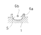
前記電送線6は、図4のa,bに示すように、蓋体1の内面に一体形成された断面半円形で、両側にシールド壁が立設されたの凹溝6a内に、中心導体として、真鍮や銅製の導電性ロッド6bを、凹溝6aの内壁と非接触状態にて配置した同軸構造となっている。
又、前記電送線6には、断面外形が凹溝6aに等しく、ロッド挿通孔が貫設された誘電体ブロック7が、凹溝6a内に、部分的且つ溝方向へ移動可能に介在されている。
このような構造の伝送線6は、ケースの内壁面に組み込まれ、中心導体としての導電性ロッド6bの太さに自由度を持たせることができるし、A−A線端面を示す図5の如く、外部導体としての凹溝6aの内壁と導電性ロッド6bとの間に空気層Sが確保されるため、伝送損失が少なく、高い電流値に対応させることができるばかりか、誘電体ブロック7を溝方向へ移動させることによって高周波特性を変化させ、適正な高周波特性に調整できる。
この誘電体ブロック7は、ジュラコン(商品名:ポリプラスチックス株式会社製)で形成することが好ましく、前記ジュラコンと電気的特性が同様な他の合成樹脂で形成したり、設計段階で予め位置が決まっている場合は、図6に例示するように、凹溝6a内に複数(二個)設けたり、固定式とすることができる。
その場合、図示のように各誘電体ブロック7,7を上下二つニ分割し、上半分の2個をアーム7aで連結し、そのアーム7aを蓋体1にねじ止めするようにすれば、効率良く組み込むことができる。
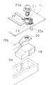
又、導電性ロッド6bには、その一端の延長上に、スリット入りの割り筒8が一体的に固着されており、その割り筒8はケーブル接続部3(2,4)において、挟持ブロック9により挟持した状態で支持されている。
前記挟持ブロック9は、片側をヒンジ構造とし、分割面に割り筒保持用の保持溝9aが形成されていて、その挟持ブロック9を、蓋体1の内面におけるケーブル接続位置に、部前記凹溝6aと連続して形成されたブロック収納部9b内に位置決めし、前記割り筒8を保持溝9aに当てがって挟み込んで、B−B端面を示す図7の如く、側方よりねじ9cにより締着されるようになっている。
従って、電送ケーブルの端部に取り付けたコネクタ10を蓋体1のコネクタねじ込み孔3a(2b,4c)にねじ込み、コネクタ10のピン10aを前記割り筒8に挿し込んでねじ9cを締着すれば、コネクタ10のピン10aと割り筒8とが挟持ブロック8にて強固且つ確実に締着結合される。
尚、前記挟持ブロック8には、ねじとの当接面に金属製の当て板8aが取り付けられていて、挟持ブロック8の割れや変形の防止とともに、締着圧が全面に作用する働きを持っており、前記ねじ9cの締着操作は、盲ボルト3b(2b,4b)を外すことによりねじ締め操作用孔を介して外部より可能となる。
【0007】
11はマザーボードで、裏面には前記幹線接続端子5a,5b(5b,5c)の距離に相当する間隔で、入出力端子としての送電端子12,12が、又表面には、中継端子13,13が設けられ、その中継端子13と前記送電端子12とは、夫々コンデンサ14aを介在させ、高周波信号の通過を許容した高周波通過回路14で結ばれ、更に前記送電端子12,12間は、コイル15aを介在させた電流通過回路15により接続されている。
尚、前記電流通過回路15はカバーで覆われている。
マザーボード11には、蓋体1に突設されたガイドピン16,16・・に対応してガイド穴17,17・・が設けられており、前記幹線接続端子5a,5b、5cが装着時に見えなくてもそのガイド穴17に前記ガイドピン16を夫々挿入することによって、例えば送電端子12,12が夫々幹線接続端子5a,5bに接続されるよう容易に位置決めすることができ、ねじ18,18により蓋体1に固定される。
前記マザーボード11には、送電端子12,12の位置にもねじが設けられ、送電端子12と幹線接続端子5b(5a,5c)とが圧接状態で接続される。
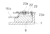
即ち、各幹線接続端子5a,5b、5cは、前記凹溝6aのデッドエンド部(図4参照)に、樹脂製の台座19を設け、その台座19の上に、ねじ穴20が形成された導電性ロッド6bの端部を位置せしめ、一方マザーボード11には、図8の如く、ねじ穴21の周囲に第1のランド部22を設け、導電性を有する例えば真鍮や鉄などの材質で形成されたねじ22aを幹線接続端子5bのねじ穴20に螺合させることによって、ねじ22aの頭部を前記第1のランド部22に密着させ、第1のランド部22と導電性ロッド6bとを電気的に接続する。
尚幹線接続端子5b(5a,5c)は、導電性ロッド6bが前記図6のように、二個の誘電体ブロック7,7によって凹溝6a内で確実に支持されている場合は、台座を省略することもできる。
又、前記第1のランド部22の外側には、その第1のランド部22と絶縁され、一部が切り欠かれたリング状の第2のランド部23が同心円上に形成され、その第2のランド部23は、裏面に突設された接触片23aを介して蓋体1と電気的に接続され、幹線接続端子5b(5a,5c)は送電端子12と同軸に接続される(図9)。
更に、マザーボード11には、送電端子12,12の外側にあたる位置に、夫々スリット状の係止孔24,24が形成されている。
【0008】
25は、箱状の分岐ユニットであり、この分岐ユニット25の片面には前記マザーボード11の中継端子13,13に対応した接続端子26,26´が、他面には分岐端子27が夫々設けられ、それら接続端子26,26´と分岐端子27とは、内蔵された分岐回路に接続されている。
又前記分岐ユニット25は、一方の接続端子26が入力側、他方の接続端子26´が出力側に設定され、高周波信号に対して方向性を有しており、その分岐ユニット25の両側には、接続端子26,26´が設けられている面側に向けて係止爪28,28が突設されている。
そしてこの分岐ユニット25は、前記マザーボード11に対し、係止爪28,28を係止孔24,24に挿入することにより係止させれば、各中継端子13,13と接続端子26,26´とが接続された状態で装着される。
尚、マザーボードに対する分岐ユニットの装着手段は、案内片を係止孔に係止させたり、ねじやクリップを利用して固定する等、適宜変更して差し支えない。前記マザーボード11にはプッシュ式のスイッチ29が設けられており、分岐ユニット25を装着すると、その分岐ユニット25の外表面で押圧操作されることによってOFF作動し、分岐ユニット25を外すことによって押圧が解除されるとON作動して両中継端子13,13間を短絡させ、送電端子12,12間に、高周波信号の通過を許容するようになっている。
前記マザーボード11は電流通過回路15を備えているから、分岐ユニット25が装着されているか否かに拘らず、送電端子12,12には、電流と高周波信号との通過機能が確保されるのである。
【0009】
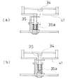
30はタップボードであり、このタップボード30は、ケースを構成するもう一方の部材である本体31の内面に組み付けられていて、分配回路と、本体表面に露出される4つの分岐出力端子として機能する分配端子32,32・・とを有し、内面には前記分岐ユニット25の分岐端子27に対応した入力端子33を備え、又、蓋体1のケーブル接続部3aと本体31の分配回路との相互間には、電流の通過を許容する電流通過用接点34,35が設けられていると共に、その電流通過用接点34と各分岐出力端子としての分配端子32,32・・との間を個々に結ぶ電流通過用回線36がタップボード30に組み込まれていて、本体31を、蓋体1の開口面を覆うように取り付けることによって、入力端子33が前記分岐端子27に接続されると共に、電流通過用接点34,35同士が接続状態となり、高周波通過経路とは別に、独立した電流通過経路が形成される。
前記電流通過用接点35は、図10に示すように、タップボード30のプリント基板に対し、基端部をハンダ付けすることによって起立固定され、コイルスプリング35aによって突出先端方向に付勢されたピンタイプであって、挿入タイプの電流通過用接点34に対して位置ずれしている場合には、電流通過用接点35の先端が例えば後述する保護プレート41に当接するので、電流通過用接点35がコイルスプリング35aを圧縮させて後退していて(図11のa)、蓋体1を本体31に対して相対的にずらせると、そのずれ量に応じてスムーズに移動し、両接点が一致したときに、電流通過用接点35が突出し、その電流通過用接点35は、コイルスプリング35aの圧縮力によって確実に接続される(図11のb)ようになっている。
又、電流通過用回線36には、正特性サーミスタ(商品名:ポリスイッチRXE065・株式会社レイケム製)37が介在され、その正特性サーミスタ37は、各分配出力端子に対して個々に設けられると共に、電流通過用回線に接続されているコネクタ(商品名:VHシリーズコネクタ・日本圧着端子株式会社製)38に対して抜き挿し操作することにより、ワンタッチで着脱できる状態にて備えられている。
そして前記蓋体1と本体31とは、左右の嵌合部を異なる形状にして、組み付ける場合に方向性を持たせてあり、蓋体1に突設された舌片39を本体31に形成された案内溝40内に挿入させることによってのみ組み付け可能で、左右逆の場合は組み付けができず、組み付けた場合には必ず前記電流通過用接点34,35が接続されるようになっている。
又前記電流通過用接点34は、ケーブル接続部3に位置する割り筒と電流通過ケーブル34aで接続され、通常その上面が、端子差込み孔41aを有した保護プレート41で覆われており、作業中に指先等を誤って電流通過用接点34に接触させる感電事故から守られている。
そして前記保護プレート41は、絶縁性に優れ、且つ電流通過用接点35の先端を当接させたままでスムーズにずらせられるよう、ABZ樹脂等の滑りやすい材料で形成されている。
【0010】
このように形成された分岐器は、分岐ユニット25の接続端子26がケーブル接続部2側に、接続端子26´がケーブル接続部3側に夫々接続されるように装着すれば、図12のaに示す如く、ケーブル接続部2を入力端子、ケーブル接続部3を出力端子としたエアリアルタイプとして機能する。
ここで入力端子と出力端子とを逆の配置にしたい場合は、分岐ユニット25を一旦外し、180度水平回転させ、中継端子13,13に対して接続端子26,26´を逆に接続するだけで簡単に変更できる(図12のb)。
又、ペデスタルタイプに対応できるようにするには、マザーボード11を一旦外し、図12のcの如く時計方向に90度回転させれば、接続端子26,26´が送電端子12,12を介して夫々幹線接続端子5b,5cに接続され、ケーブル接続部3を入力端子、ケーブル接続部4を出力端子に変更できる。
入力端子と出力端子とを逆の配置にしたい場合は、図示はしないが、前記エアリアルタイプと同様に、分岐ユニット25を一旦外し、180度水平回転させて逆に接続されるよう付け替えるだけで簡単に変更できる。
更に、分岐数を変更したい場合は、タップボード30が組み付けられた本体31と、マザーボード11に装着されている分岐ユニット25とを所望の分岐数に対応した分配器が組み付けられた別の本体と分岐ユニットに交換することにより可能である。
この交換に際し、分岐ユニット25は、係止爪28と係止穴24との係止を解除するだけで外すことができ、又、分岐ユニット25を外すと、スイッチ29がON作動して送電端子12,12間が短絡され、高周波信号の通過が許容されるので、ケーブル接続部間における高周波信号の伝達が途絶えることはない。
【0011】
このように実施例の分岐器は、マザーボードを90度回動させたり、分岐ユニットと本体とを交換するだけで、ケーブル接続部の位置や分岐数を変更できるから、操作性に優れ、一機種で複数タイプに対応できるし、分岐ユニットや本体を外しても入力側から出力側への電流や高周波信号の通過が遮断されることがなく、チェック機能が維持される。
又このとき伝送ケーブルを電話回線として使用している場合でも、電話は低周波領域をを利用しているので、電流通過用回路及び回線の使用によって通話が中断されることはない。
一方、電流通過用回線には正特性サーミスタが介在されているので、分岐端子側で短絡事故があった場合、正特性サーミスタの抵抗値が0.数Ωから数KΩ以上にまで増大し、伝送ケーブルに対するケーブル接続部と分岐出力端子間の電流の通過が阻止され、分岐器内の回路を保護すると共に、伝送ケーブルに接続されている機器への悪影響を阻止し、15アンペアを通電するような大電流通過型であっても安心して採用できる。
而もその際、高周波信号の伝送回路(分岐回路)が電流通過用回線と別個独立し、且つ正特性サーミスタが個々の分岐出力端子に対して個々に介在されているので、電流の通過が阻止されても、テレビ信号が途絶えたりすることはないばかりか、短絡した分岐出力端子へのみの電力通過機能が阻止されるに留まる。
又正特性サーミスタは、各分岐端子に対して個々に、而も着脱自在に設けられているので、電話回線利用加入者の家庭に接続される特定の端子のみを電流通過タイプとし、未加入者の家庭に接続される端子に対しては、正特性サーミスタをコネクタから外し、電流の供給がされないように設定することが簡単にできるし、一見しただけで確認も容易である。
このような効果は、コネクタに対して正特性サーミスタを着脱自在とすることなく、図示はしないが、電流通過用回線にスイッチを設け、そのスイッチのON/OFF操作で制御することによっても可能である。
【0012】
そして各端子接続部は、二回線分のみとしたり、分岐数は、増加させるばかりでなく減少させる場合もあって、本体の分岐数はいくつでもかまわない。
又実施例は、幹線接続端子を、蓋体の中心を挟んだ上部左右の二箇所と、その二箇所のうちの片側に対して上下関係となる一箇所との計三箇所に配置し、マザーボードを回転させてそのマザーボードの送電端子に接続される幹線接続端子を選択するものであるが、対として選択される幹線接続端子を、相互の間隔が等しくなるよう配置し、マザーボードをずらせたり移動させて組み付け位置を変えることにより、接続すべき幹線接続端子と接続されるようにすることもできるし、そのようなケーブル接続部の使い分け、或は分岐端子の数の変更を要しない機種にも適用される。
マザーボードの組み付け位置を替える場合は、ねじの着脱操作によって可能であり、そのねじの締着操作で、伝送線の中心導体である金属ロッドの端部と、マザーボードの入出力端子としての送電端子とが確実に接続され、加熱の虞れはない。
【0013】
【発明の効果】
本発明によれば、マザーボードの入出力端子と、樹脂製の台座上に位置決めされた伝送線の中心導体端部とが、ねじによって確実に接続されるから、大電流に対して充分な容量が確保され、電流通過回路を介して接続される入出力用ケーブル接続部間の伝送損失が低減され、発熱による特性への影響がなくなる。
又、複数のケーブル接続部を設定しておき、そのケーブル接続部を選択可能とすれば、エアリアルタイプとぺデスタルタイプとに使い分けできる。
更に、伝送線を、ケースの内壁面に形成された凹溝内に、その凹溝と非接触状態で配置した構造とすることで、伝送損失を極限にまで減らすことができる。
【図面の簡単な説明】
【図1】 本発明に係る分岐器の実施例を示す分解説明図である。
【図2】 各部材の平面図である。
【図3】 各部材の回路を示す説明図である。
【図4】 伝送線の説明図である。
【図5】 図4のA−A線端面図である。
【図6】 伝送線の変更例を示す説明図である。
【図7】 図4のB−B線端面図である。
【図8】 幹線接続端子の説明図である。
【図9】 幹線接続端子とマザーボドとの接続部を示す説明図である。
【図10】 電流通過用接点の説明図である。
【図11】 電流通過用接点の動作説明図である。
【図12】 ケーブル接続部の変更例を示す説明図である。
【符号の説明】
1・・蓋体、2,3,4・・ケーブル接続部、2a,3a,4a・・コネクタねじ込み孔、2b,3b,4b・・盲ボルト、5・・回路収容部、5a、5b,5c・・幹線接続端子、6・・伝送線、6a・・凹溝、6b・・導電性ロッド、7・・誘電体ブロック、7a・・アーム、8・・割り筒、8a・・当て板、9・・挟持ブロック、9a・・保持溝、9b・・ブロック収納部、9c・・ねじ、10・・コネクタ、10a・・ピン、11・・マザーボード、12・・送電端子、13・・中継端子、14・・高周波通過回路、14a・・コンデンサ、15・・電流通過回路、15a・・コイル、16・・ガイドピン、17・・ガイド穴、18・・ねじ、19・・台座、20・・ねじ孔、21・・ねじ挿通孔、22・・第1のランド部、22a・・ねじ、23・・第2のランド部、23a・・接触片、24・・係止孔、25・・分岐ユニット、26・・接続端子(入力側)26´・・接続端子(出力側)、27・・分岐端子、28・・係止爪、29・・スイッチ、30・・タップボード、31・・本体、32・・分配端子(分岐出力端子)、33・・入力端子、34,35・・電流通過用接点、34a・・電流通過ケーブル、35a・・コイルスプリング、36・・電流通過用回線、37・・正特性サーミスタ、38・・コネクタ、39・・舌片、40・・案内溝、41・・保護プレート、41a・・端子差込み孔、P・・中心点、S・・空気層。[0001]
[Industrial application fields]
The present invention relates to a branching device, particularly to a branching device suitable for CATV.
[0002]
[Prior art]
For the branching device used in CATV, a plurality of models must be set depending on the position of the input / output cable connection part and the number of branches, but the internal mechanism is, for example, a motherboard with a current passing circuit and a branching circuit. A general-purpose type has been proposed in which a branch circuit and a branch circuit are unitized, and each unit is recombined according to the application to suit the purpose of use.
On the other hand, the CATV transmission cable is supplied with a high-frequency signal such as a television signal and a control signal, and also a current for operating amplifiers of the trunk amplifier.
For this reason, the branching device also has a current passing specification, and in the case of the current passing specification, it is not preferable that the current pass through the branch circuit or the branching circuit. The structure is such that the input / output cable connection portions are connected via a current passage circuit.
A plug-in type is adopted for the connection portion between the transmission cable and the mother board directly connected to the input / output cable connection portion.
[0003]
[Problems to be solved by the invention]
In the case of current passing specifications, the current value sent to each branch terminal is low, but since the maximum current flowing through the trunk line passes at least between the cable connection parts, the transmission loss between the input / output cable connection parts is reduced, We must avoid affecting the characteristics of radio waves as much as possible.
However, if the connection portion is a plug-in type, not only transmission loss is likely to occur, but if the value of the current flowing through the main line is high, heat is generated, which may impair the characteristics of the circuit mounted on the motherboard.
[0004]
[Means for Solving the Problems]
The present invention has a built-in motherboard including a branch circuit that branches and outputs a high-frequency signal input from an input terminal and a current passage circuit that allows current to pass between input and output terminals at a substantially central position in the case. A branching device that is inserted and connected in the middle of the cable, and is provided with a screw hole at the end portion of the center conductor of the transmission line that electrically connects the cable connection portion provided on the side portion of the case and the input / output terminal of the motherboard. On the other hand, a land portion is provided around the screw insertion hole in the mother board, and a conductive screw inserted through the screw insertion hole is screwed into the screw hole of the central conductor, and the transmission line and the input / output of the mother board through the screw. This is because the terminals are electrically connected.
In the branching device, three or more cable connection portions are set, and two cable connection portions to be connected to the motherboard can be selected from the three or more cable connection portions, or the transmission line The central conductor is disposed in a concave groove formed on the inner wall surface of the case in a non-contact state with the concave groove, and a connecting portion for the mother board can be assembled to the dead end portion of the concave groove.
[0005]
【Example】
An embodiment of a branching device according to the present invention will be described based on the drawings with respect to a model in which cable connection portions are set for three lines, and aerial type and pedestal type can be selectively used and the number of branch terminals can be changed. To do.
1, 2, and 3,
In addition, the
[0006]
As shown in FIGS. 4a and 4b, the
In addition, a
The
The
In that case, if each
In addition, a
The
Therefore, if the
The
[0007]
The
The
The
That is, each main
The main
A ring-shaped
Further, the
[0008]
Further, the
When the
Note that the branch unit mounting means for the mother board may be changed as appropriate, such as locking the guide piece in the locking hole or fixing it using a screw or clip. The
Since the
[0009]
As shown in FIG. 10, the current passing
Further, a positive temperature coefficient thermistor (trade name: Polyswitch RXE065, manufactured by Raychem Co., Ltd.) 37 is interposed in the current passing
The
The current passing
The
[0010]
When the branching device thus formed is mounted so that the
Here, if the input terminal and the output terminal are to be reversed, the
Also, in order to be compatible with the pedestal type, once the
If you want to reverse the input terminal and the output terminal, not shown, but as with the aerial type, simply remove the
Further, when it is desired to change the number of branches, the
At the time of this replacement, the
[0011]
In this way, the branching device of the embodiment is excellent in operability because the position of the cable connection part and the number of branches can be changed by simply rotating the motherboard 90 degrees or replacing the branching unit and the main body. It can handle multiple types, and even if the branch unit or main body is removed, the current and high-frequency signal from the input side to the output side are not blocked, and the check function is maintained.
Even when the transmission cable is used as a telephone line at this time, since the telephone uses the low frequency region, the telephone call is not interrupted by the use of the current passing circuit and the line.
On the other hand, since a positive temperature coefficient thermistor is interposed in the current passing line, if there is a short circuit accident on the branch terminal side, the resistance value of the positive temperature coefficient thermistor is 0. Increases from several Ω to several KΩ or more, prevents the passage of current between the cable connection to the transmission cable and the branch output terminal, protects the circuit in the branching unit, and connects to the equipment connected to the transmission cable. Even a large current passing type that prevents adverse effects and energizes 15 amps can be used with confidence.
At that time, the high-frequency signal transmission circuit (branch circuit) is independent of the current passage line, and the positive temperature coefficient thermistor is individually provided for each branch output terminal, thus preventing the passage of current. In this case, the television signal is not interrupted, and the power passing function only to the shorted branch output terminal is prevented.
In addition, since the positive temperature coefficient thermistor is detachably provided individually for each branch terminal, only a specific terminal connected to the home of the telephone line subscriber is a current passing type, and the non-subscriber For the terminals connected to the home, it is easy to remove the positive temperature coefficient thermistor from the connector and set it so that no current is supplied, and it is easy to confirm at first glance.
Such an effect can also be achieved by providing a switch on the current passing line and controlling it by ON / OFF operation of the switch, although not shown, without making the positive thermistor detachable from the connector. is there.
[0012]
Each terminal connection section may have only two lines, or the number of branches may be decreased as well as increased, and the number of branches in the main body is not limited.
Further, in the embodiment, the main line connection terminals are arranged at three places in total, that is, two places on the upper left and right sides of the center of the lid, and one place that is vertically related to one of the two places. The main line connection terminals that are connected to the power transmission terminal of the motherboard are selected, but the main line connection terminals that are selected as a pair are arranged so that the distance between them is the same, and the motherboard is shifted or moved. By changing the assembly position, it can be connected to the main connection terminal to be connected, and it is also applicable to models that do not require different use of such cable connection parts or change of the number of branch terminals Is done.
When changing the assembly position of the motherboard, it can be done by attaching and detaching the screw, and by fastening the screw, the end of the metal rod that is the center conductor of the transmission line and the power transmission terminal as the input / output terminal of the motherboard Are securely connected and there is no risk of heating.
[0013]
【The invention's effect】
According to the present invention, the input / output terminals of the motherboard and the center conductor end of the transmission line positioned on the resin base are securely connected by the screw, so that a sufficient capacity for a large current is obtained. The transmission loss between the input / output cable connecting portions secured through the current passing circuit is reduced, and the influence of the heat generation on the characteristics is eliminated.
If a plurality of cable connection portions are set and the cable connection portions can be selected, the aerial type and the pedestal type can be used properly.
Furthermore, the transmission loss can be reduced to the utmost by adopting a structure in which the transmission line is disposed in a concave groove formed on the inner wall surface of the case in a non-contact state with the concave groove.
[Brief description of the drawings]
FIG. 1 is an exploded explanatory view showing an embodiment of a branching device according to the present invention.
FIG. 2 is a plan view of each member.
FIG. 3 is an explanatory diagram showing a circuit of each member.
FIG. 4 is an explanatory diagram of a transmission line.
FIG. 5 is an end view taken along line AA in FIG. 4;
FIG. 6 is an explanatory diagram showing a modification example of a transmission line.
7 is an end view taken along the line BB in FIG. 4. FIG.
FIG. 8 is an explanatory diagram of a main line connection terminal.
FIG. 9 is an explanatory diagram showing a connection portion between a main line connection terminal and a motherboard.
FIG. 10 is an explanatory diagram of a current passing contact.
FIG. 11 is an operation explanatory diagram of a current passing contact;
FIG. 12 is an explanatory view showing a modification example of the cable connecting portion.
[Explanation of symbols]
1 .. Lid, 2, 3, 4 .. Cable connection part, 2a, 3a, 4a .. Connector screw hole, 2b, 3b, 4b .. Blind bolt, 5 .. Circuit housing part, 5a, 5b, 5c ..Main line connection terminal, 6 ..Transmission line, 6a ..Concave groove, 6b ..Conductive rod, 7 ..Dielectric block, 7a ..Arm, 8 .. Split tube, 8a. ··· Holding block, 9a · · Holding groove, 9b · · Block housing portion, 9c · · Screw, 10 · · Connector, 10a · · Pin, 11 · · Motherboard, 12 · · Power transmission terminal, · · · Relay terminal, 14 .. High frequency passing circuit, 14 a .. Capacitor, 15 .. Current passing circuit, 15 a .. Coil, 16 .. Guide pin, 17 .. Guide hole, 18 .. Screw, 19 .. Pedestal, 20. Hole, 21 .. screw insertion hole, 22 .. first land portion, 22a · Screw, 23 ··· Second land portion, 23a · · Contact
Claims (3)
Priority Applications (3)
| Application Number | Priority Date | Filing Date | Title |
|---|---|---|---|
| JP26590295A JP3677097B2 (en) | 1995-10-13 | 1995-10-13 | Turnout |
| PCT/JP1996/002111 WO1997014197A1 (en) | 1995-10-13 | 1996-07-24 | Branching device |
| US08/849,698 US5973262A (en) | 1995-10-13 | 1996-07-24 | Multi-tap distribution apparatus |
Applications Claiming Priority (1)
| Application Number | Priority Date | Filing Date | Title |
|---|---|---|---|
| JP26590295A JP3677097B2 (en) | 1995-10-13 | 1995-10-13 | Turnout |
Publications (2)
| Publication Number | Publication Date |
|---|---|
| JPH09116369A JPH09116369A (en) | 1997-05-02 |
| JP3677097B2 true JP3677097B2 (en) | 2005-07-27 |
Family
ID=17423695
Family Applications (1)
| Application Number | Title | Priority Date | Filing Date |
|---|---|---|---|
| JP26590295A Expired - Fee Related JP3677097B2 (en) | 1995-10-13 | 1995-10-13 | Turnout |
Country Status (3)
| Country | Link |
|---|---|
| US (1) | US5973262A (en) |
| JP (1) | JP3677097B2 (en) |
| WO (1) | WO1997014197A1 (en) |
Families Citing this family (8)
| Publication number | Priority date | Publication date | Assignee | Title |
|---|---|---|---|---|
| US6157548A (en) * | 1999-03-25 | 2000-12-05 | Illinois Tool Works Inc. | Electrically shielded housing |
| US20060150232A1 (en) * | 2004-12-30 | 2006-07-06 | Karpati George S | Tap bypass assembly |
| US7198491B2 (en) * | 2005-01-18 | 2007-04-03 | Lockheed Martin Corporation | Multi-pin RF field replaceable coaxial mounting flange structure |
| US7830225B2 (en) * | 2005-06-13 | 2010-11-09 | Gale Robert D | Electric signal splitters |
| US7375533B2 (en) * | 2005-06-15 | 2008-05-20 | Gale Robert D | Continuity tester adaptors |
| JP6370429B2 (en) | 2016-03-31 | 2018-08-08 | モレックス エルエルシー | Cable tray assembly |
| JP6939663B2 (en) * | 2018-03-14 | 2021-09-22 | オムロン株式会社 | socket |
| CN217485687U (en) * | 2019-07-31 | 2022-09-23 | 康普技术有限责任公司 | Phase line keeper |
Family Cites Families (15)
| Publication number | Priority date | Publication date | Assignee | Title |
|---|---|---|---|---|
| US3617811A (en) * | 1970-07-22 | 1971-11-02 | Coaxial Scient Corp | Cable television tapoff unit |
| JPS5255962A (en) * | 1975-10-31 | 1977-05-07 | Yanmar Agricult Equip | Thresher |
| JPS62196435A (en) * | 1986-02-21 | 1987-08-29 | Babcock Hitachi Kk | Deviated-load cylindrical article rotating device |
| JPS6320156A (en) * | 1986-07-14 | 1988-01-27 | Hitachi Metals Ltd | Parts for solder processor |
| JPS6325801A (en) * | 1986-07-17 | 1988-02-03 | Matsushita Electric Ind Co Ltd | Magnetic field generating method |
| US4755776A (en) * | 1987-03-06 | 1988-07-05 | Broadband Networks, Inc. | Tap device for broadband communications systems |
| JPH02119362A (en) * | 1988-10-27 | 1990-05-07 | Nec Corp | Telephone number mobile service system |
| JPH02119362U (en) * | 1989-03-10 | 1990-09-26 | ||
| US5058198A (en) * | 1989-03-31 | 1991-10-15 | Am Communications, Inc. | Radio frequency tap unit which can be reconfigured with minimal disruption of service |
| US4963966A (en) * | 1989-12-04 | 1990-10-16 | Scientific Atlanta, Inc. | CATV distribution system, especially adapted for off-premises premium channel interdiction |
| US4995815A (en) * | 1990-02-26 | 1991-02-26 | At&T Bell Laboratories | Coaxial transmission line to strip line coupler |
| NL9200272A (en) * | 1992-02-14 | 1993-09-01 | Du Pont Nederland | COAX CONNECTOR MODULE FOR MOUNTING ON A PRINTED WIRING PLATE. |
| JPH06283871A (en) * | 1993-03-29 | 1994-10-07 | Nec Kansai Ltd | Fixing structure for printed board |
| JPH08181559A (en) * | 1994-12-22 | 1996-07-12 | Maspro Denkoh Corp | High frequency signal branching device |
| US5613859A (en) * | 1995-11-28 | 1997-03-25 | Watkins-Johnson Company | Connector asembly for detachably connecting a printed wiring board to a coaxial transmission lines connector |
-
1995
- 1995-10-13 JP JP26590295A patent/JP3677097B2/en not_active Expired - Fee Related
-
1996
- 1996-07-24 US US08/849,698 patent/US5973262A/en not_active Expired - Fee Related
- 1996-07-24 WO PCT/JP1996/002111 patent/WO1997014197A1/en active Application Filing
Also Published As
| Publication number | Publication date |
|---|---|
| WO1997014197A1 (en) | 1997-04-17 |
| JPH09116369A (en) | 1997-05-02 |
| US5973262A (en) | 1999-10-26 |
Similar Documents
| Publication | Publication Date | Title |
|---|---|---|
| US10269524B2 (en) | Multiple fuse device | |
| JP3677097B2 (en) | Turnout | |
| US5545848A (en) | Cassette splitter for television antenna signals | |
| JP3677099B2 (en) | Turnout | |
| JP3700869B2 (en) | Turnout | |
| JP3076960B2 (en) | Switch | |
| EP0786832B1 (en) | Branching device | |
| WO1995004392A1 (en) | Multi-position electrical connector and electrical devices incorporating same | |
| JP3703887B2 (en) | Turnout | |
| AU6872400A (en) | Switch/inlet unit and entertainment device | |
| JP4076183B2 (en) | Switch device-Printed wiring board-Combination | |
| US5928021A (en) | Electrical connector with internal switch and mating connector therefor | |
| JPH08293363A (en) | Connection converting connector | |
| JPH06223892A (en) | Terminal board | |
| JP3664323B2 (en) | High frequency signal processor | |
| US6653559B2 (en) | Complex-shaped terminal board, in particular for high-current applications | |
| JPH0594755A (en) | Electronic circuit breaker having terminal connecting block | |
| JPH0688076U (en) | I / O connector | |
| JPH1093372A (en) | Branching device | |
| JP2802888B2 (en) | connector | |
| EP1360743A1 (en) | Printed circuit board and connector assembly | |
| JPH09115620A (en) | Coaxial conversion connector | |
| JPH0279378A (en) | Wiring accessory for image signal | |
| JPH03270288A (en) | Electric connector | |
| JPH03149929A (en) | Interception preventing device |
Legal Events
| Date | Code | Title | Description |
|---|---|---|---|
| TRDD | Decision of grant or rejection written | ||
| A01 | Written decision to grant a patent or to grant a registration (utility model) |
Free format text: JAPANESE INTERMEDIATE CODE: A01 Effective date: 20050405 |
|
| A61 | First payment of annual fees (during grant procedure) |
Free format text: JAPANESE INTERMEDIATE CODE: A61 Effective date: 20050506 |
|
| R150 | Certificate of patent or registration of utility model |
Free format text: JAPANESE INTERMEDIATE CODE: R150 |
|
| FPAY | Renewal fee payment (event date is renewal date of database) |
Free format text: PAYMENT UNTIL: 20090513 Year of fee payment: 4 |
|
| FPAY | Renewal fee payment (event date is renewal date of database) |
Free format text: PAYMENT UNTIL: 20100513 Year of fee payment: 5 |
|
| FPAY | Renewal fee payment (event date is renewal date of database) |
Free format text: PAYMENT UNTIL: 20110513 Year of fee payment: 6 |
|
| FPAY | Renewal fee payment (event date is renewal date of database) |
Free format text: PAYMENT UNTIL: 20120513 Year of fee payment: 7 |
|
| LAPS | Cancellation because of no payment of annual fees |