JP3671859B2 - Portable radio - Google Patents
Portable radio Download PDFInfo
- Publication number
- JP3671859B2 JP3671859B2 JP2001130783A JP2001130783A JP3671859B2 JP 3671859 B2 JP3671859 B2 JP 3671859B2 JP 2001130783 A JP2001130783 A JP 2001130783A JP 2001130783 A JP2001130783 A JP 2001130783A JP 3671859 B2 JP3671859 B2 JP 3671859B2
- Authority
- JP
- Japan
- Prior art keywords
- antenna
- flip
- metal shield
- ground
- shield housing
- Prior art date
- Legal status (The legal status is an assumption and is not a legal conclusion. Google has not performed a legal analysis and makes no representation as to the accuracy of the status listed.)
- Expired - Fee Related
Links
Images


Description
【0001】
【産業上の利用分野】
この発明は携帯無線機に関し、特に小型化されたものに適用して好適なものである。
【0002】
【従来の技術】
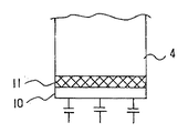
従来、この種の携帯無線機は、図11に示すように、スリーブアンテナやλ/2、3λ/8又はλ/4系のホイップアンテナ5が無線部を内蔵する金属シールド筐体4に装着されている。スリーブアンテナやλ/2系のホイップアンテナは金属シールド筐体4の下端、すなわちアンテナ接地部の反対側において、アンテナ電流分布が0となるためインピーダンスがオープンであり、放射パターンにおいて金属シールド筐体4の大きさや長さ等から影響を受けることはほとんどない。
【0003】
ところが給電側とのマッチングが困難なことや、アンテナ全長が長くなることから、一般には3λ/8又はλ/4系のホイップアンテナ5が使用されることが多い。これらのアンテナ5では、金属シールド筐体4もアンテナの一部となるため金属シールド筐体4の大きさ、長さといったパラメータは、放射パターン、指向性といったアンテナの性能にとって非常に重要である。
【0004】
また携帯無線機は、フリップがないか又はフリップが有ってもフリップ内に部品がなく、フリップ自体で集音効果をねらった構造が主となっていた。実際上フリップがない構造では、マイク等は金属シールド筐体4内に納められている。そしてこれらのリード線は金属シールド筐体4内部に配されているため、金属シールド筐体4からは突出がなく、アンテナの地板としては金属シールド筐体4のみをとらえ、この結果放射パターン、指向性といったアンテナの性能に影響を与えることはなかった。
【0005】
【発明が解決しようとする課題】
ところで最近の携帯無線機においては、小型化が進んだために集音効果や通話時の安定感を考慮して、フリップ構造を持つものが多くなってきた。そして、このフリップ内にマイク、スイッチ、その他いろいろな電子部品を納める構成のものがある。
【0006】
ところがこのようにフリップ内に電子部品を納めるようになされた携帯無線機において、フリップを閉じているときはそれらのリード線のグランド側は、金属シールド筐体4に非常に近いために、リード線のインピーダンスは低くアンテナ性能に影響を与えないが、フリップを開くとリード線のインピーダンスが高くなり、金属シールド筐体4より突き出たグランドの一部となる。
【0007】
このためアンテナの電流分布が変化し、アンテナ放射パターンに大きな影響を与える。金属シールド筐体4をアンテナの一部と考えるλ/4、3λ/8系のアンテナを有する携帯無線機においては、金属シールド筐体4にも電流が多く流れているので、特に顕著に指向性や放射パターン等のアンテナの性能に影響が現れてしまう問題があった。
【0008】
この発明は上記のような課題を解消しようとするもので、フリップ内に電子部品を配置した場合の放射パターンや指向性等のアンテナの性能に与える影響を有効に除去すると共に、フリップの有無にかかわらずアンテナの指向性や放射パターンを任意に設定し得る携帯無線機を提供することを目的とする。
【0009】
【課題を解決するための手段】
上記の課題を解決するため、この発明の請求項1に係る携帯無線機は、アンテナ、このアンテナの地板となるグランドを有する基板、この基板上に設けられ誘導性または容量性を有する素子を備え、この素子の一端がオープンであり、他端が前記グランドのアンテナ設置部から離れた端部に接続されるものである。
【0010】
また、この発明の請求項2に係る携帯無線機は、アンテナ、このアンテナの地板となるグランドを有する基板、この基板上に形成され誘導性を有するパターンを備え、このパターンの一端がオープンであり、他端が前記グランドのアンテナ設置部から離れた端部に接続されるものである。
【0012】
【作用】
金属シールド筐体でアンテナ設置部に対して反対の下部に、または金属シールド筐体の下部より下に内蔵された基板のグランド部分がある場合にはその基板のグランド部分に、片端オープンのチップ部品を配し、金属シールド筐体のみかけ上の長さを調節することにより、アンテナの指向性や放射パターンを任意に設定できる。
【0013】
また、内蔵された基板のグランド部分より下方に、パターンによって片端オープンのインダクタンスを形成することにより、アンテナの指向性や放射パターンを任意に設定できる。
【0015】
【実施例】
以下図面を参照しながら、この発明の参考例、実施例を詳述する。
【0016】
参考例1.
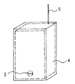
図1に、この発明による携帯無線機の参考例1の外観を示す。図中1は例えばABS樹脂等の誘電体で構成されたフリップであり、マイク2はこのフリップ中に納められている。マイクリード線3のグランド側は金属シールド筐体4に直接又は基板を介してつながっており、その長さは使用周波数のほぼλ/2(例えば周波数 900〔MHz〕の場合には、約17〔cm〕)に設定されている。フリップ1の全長に比べて使用周波数のλ/2が長い場合には、図1のようにマイクリード線3がくねらせて収納される。
【0017】
このとき、金属シールド筐体4側からマイクリード線3のグランド側を見たとき、その場所での電流分布が最少となりインピーダンスがオープンの状態となされている。すなわちフリップ1を開くと、マイクリード線3のグランド側は、使用周波数においてあたかも接続されていないように見える。またフリップ1を閉じた状態ではマイクリード線3は、金属シールド筐体4に非常に近いため、マイクロストリップラインにおいて、ライン間距離が縮まるとラインのインピーダンスが下がるのと同じ原理で、マイクリード線3のインピーダンスは低くなる。電気的には、マイクリード線3が金属シールド筐体4に埋め込まれたことと等価になる。
【0018】
従って、内部にマイク2等の電子部品を配したフリップ1が取り付けられた携帯無線機において、フリップ1を開閉しても金属シールド筐体4のアンテナ電流分布に変化は生じない。これにより、フリップ1内にマイク2を配置した場合でも、放射パターンや指向性等のアンテナの性能に与える影響を有効に除去し得る。なお、このことを考慮しないで設計すると、フリップ1を開いたときに閉じたときのアンテナ放射パターンとは全く異なる放射パターンを持つことになり、放射が所望の方向に行われずに、結果的には携帯無線機の発着呼率の低下の原因となる。
【0019】
このような構成によれば、マイク2のマイクリード線3のグランド側の長さを、使用周波数の波長λに対してλ/2に設定し、金属シールド筐体4側より見たマイクリード線3のグランド側をオープンの状態にすることにより、フリップ1の開閉によるアンテナ性能や放射パターンの影響を有効に除去し得る。
【0020】
参考例2.
図2に、この発明による参考例2の携帯無線機の外観を示す。上述の参考例1ではマイクリード線3の長さをほぼ使用周波数の波長λのλ/2としたが、この参考例2では量産時の作業性を考慮して、マイクリード線3の途中若しくはマイクリード線3と金属シールド筐体4又は基板のグランド部分との間にインダクタンス素子6を挿入することにより、電気的にλ/2の状態を作り出している。
【0021】
このようにしても、上述した参考例1と同様の効果を得ることができ、この場合、フリップ1内のマイクリード線3の配線を量産性を考慮した最短の長さに設定した後、マイクリード線3の長さとインダクタンス素子6の等価長とを加えて、使用周波数の波長λに対してλ/2となるように、インダクタンス素子6の諸元を決定でき、その分製造工程を簡略化し得ると共に量産性を向上し得る。
【0022】
参考例3.
図3に、この発明による参考例3の携帯無線機のフリップ1を示す。この参考例の場合、導電性シート7はフリップ1の中にあってどこにもつながっていない独立したグランドとなっている。このグランド上にマイクリード線3のグランド線側を近づけることによってマイクロストリップラインにおける線間距離を近づけたことと同様に、マイクリード線3のグランド側のインピーダンスを低くすることができる。
【0023】
これにより、マイクリード線3のグランド側が使用周波数の波長λに対してλ/2より短くても、フリップ1を開いた際のアンテナの性能、放射パターンに影響を与えない。この方法の場合、上述した参考例1や参考例2よりも、周波数特性に強い特徴があり、送受信周波数の帯域が離れている場合等に、極めて有効性である。フリップ1を開いても所望の方向の放射を得ることにより、携帯無線機の発着呼率をフリップ1を閉じたときと同様にできる。
【0024】
参考例4.
図4に、この発明による参考例4の携帯無線機のフリップ1を示す。この参考例では上述した参考例3における導電性シート7の代わりに、銅やアルミニウム等を金属蒸着したり、または図4に示すように部分メッキ8を施したものである。これにより参考例3と同様の効果を得ることができる。このとき、その厚みは使用周波数によって異なる表皮効果の厚さより厚くする必要がある。この方法により導電性シート7をフリップ1に貼り付ける作業を行わないで済み、その分量産性を向上し得る。
【0025】
参考例5.
図5に、この発明による参考例5の携帯無線機の本体下部及びフリップ1を示す。この実施例では、上述の参考例1〜4で行ったようにフリップ1の開閉時にアンテナ性能や放射パターンに影響を与えないようにするのでなく、通話時すなわちフリップ1を開いた状態での放射パターンが人体の影響を出来るだけ受けないようなパターンとなるようにする。フリップ1内で人体の口側に導電性シート7を貼り付けたり、または金属蒸着や部分メッキ8等を施し、電子部品のリード線3のグランド側をフリップ内の反対側に配置する。
【0026】
さらに導電性シート7と電子部品のリード線3との間に高誘電率の誘電体9を挿入することにより、両者の電気的な距離をλ/4とする。これにより、電子部品のリード線3のグランド側より放射する電波は、導電性シート7等によって反射し、人の頭と反対側に反射波と直接波が強め合って放射され、人体や頭等に吸収されることを有効に防止し得る。かくして、通話時においては発着呼率を向上することができる。
【0027】
なお上述の参考例1〜5では、フリップ1内部にマイク2を配置したが、電子部品はマイク2に限らず、スイッチやアンテナ等、さらにはLED表示手段等の種々の電子部品を配置する場合でも良く、要は電子部品のグランド側のリード線を使用周波数の波長λに対してλ/2に設定するようにすれば、上述の参考例と同様の効果を実現できる。
【0028】
実施例1.
図6及び図7に、この発明による実施例1の携帯無線機を示す。この実施例1では基板10のグランドの最下端部11にインダクタンス素子6を取付ける。このときインダクタンス素子6の片端、すなわち基板10のグランド最下端部11に接続されていない方はオープンにしておく。このインダクタンス素子6の値を変化させることにより、金属シールド筐体4の電気長を長くなる方向に変化させて、そのアンテナ電流分布を変化させる。
【0029】
例えばアンテナ5がλ/4系アンテナのとき、金属シールド筐体4の電気長も使用周波数の約λ/4であれば、アンテナ放射パターンが最適となる。金属シールド筐体4の電気長がλ/4より短いとき、この方法を用いれば、金属シールド筐体4の形状変更等を行わなくても、最適の放射パターンとすることができる。なお取付ける個数を増やすことで、金属シールド筐体4の全部を長くしたイメージができることにより、比帯域を増加させることができる。
【0030】
実施例2.
図6及び図8に、この発明による実施例2の携帯無線機を示す。この実施例2では上述した実施例1のインダクタンス素子6の代わりに、コンデンサ16を取付ける。このコンデンサ16の値を変化させることにより、金属シールド筐体4の電気長を短くなる方向に変化させて、そのアンテナ電流分布を変化させる。
【0031】
例えばアンテナ5がλ/4系アンテナのとき、金属シールド筐体4の電気長も使用周波数の約λ/4であれば、アンテナ放射パターンが最適となる。金属シールド筐体4の電気長がλ/4より長いとき、この方法を用いれば、金属シールド筐体4の形状変更等を行わなくても、最適の放射パターンとすることができる。なお取付ける個数を増やすことで、金属シールド筐体4の全部を短くしたイメージができることにより、上述の実施例1と同様に比帯域を増加させることができる。
【0032】
実施例3.
図9に、この発明による実施例3の携帯無線機を示す。この実施例3は上述した実施例1のインダクタンス素子6を部品ではなく基板のグランドの最下端部11にパターンインダクタンス12を作ることによって同様の効果を得るものである。パターンインダクタンス12の個数を増やすことで、金属シールド筐体4の全部を長くしたイメージができることにより、上述の実施例1と同様に比帯域を増加させることができる。
【0033】
実施例4.
図10に、この発明による実施例4の携帯無線機を示す。上述した実施例ではアンテナのグランド側の電気長を変えることによって、最適の放射パターンを得るようにしているが、アンテナ側を変更することでも同様の効果を得ることができる。内蔵アンテナ13は普通放射板の大きさ等を調整して共振周波数を変えるが、この実施例4では、放射板の給電点14から離れた箇所15に、片端オープンのインダクタンス素子6を取付けてアンテナの電気長を変化させ共振周波数の調整を行う。
【0034】
これにより、今までよりも少ない空間、かつ簡易な方法で共振周波数を調整できる。内蔵アンテナ13が液晶ポリマー等の成形品にメッキを施したものであれば自装も可能であり、量産性を向上し得ると共に共振周波数の調整を格段的に容易に実行し得る。
【0035】
【発明の効果】
以上のようにこの発明によれば、金属シールド筐体でアンテナ設置部に対して反対の下部に、または金属シールド筐体の下部より下に内蔵された基板のグランド部分がある場合にはその基板のグランド部分に、片端オープンのチップ部品を配し、金属シールド筐体のみかけ上の長さを調節することにより、アンテナの指向性や放射パターンを任意に設定し得る携帯無線機を実現できる。
【0036】
また、次の発明によれば、内蔵された基板のグランド部分より下方に、パターンによって片端オープンのインダクタンスを形成することにより、アンテナの指向性や放射パターンを任意に設定し得る携帯無線機を実現できる。
【図面の簡単な説明】
【図1】 この発明による携帯無線機の参考例1の全体構成を示す略線的斜視図である。
【図2】 この発明による携帯無線機の参考例2の全体構成を示す略線的斜視図である。
【図3】 この発明による携帯無線機の参考例3のフリップの構成を示す略線図である。
【図4】 この発明による携帯無線機の参考例4のフリップの構成を示す略線図である。
【図5】 この発明による携帯無線機の参考例5のフリップ廻りの構成を示す断面図である。
【図6】 この発明による携帯無線機の実施例1及び2の構成を示す略線的斜視図である。
【図7】 図6を補足してこの発明による携帯無線機の実施例1を示す略線図である。
【図8】 図6を補足してこの発明による携帯無線機の実施例2を示す略線図である。
【図9】 この発明による携帯無線機の実施例3の全体構成を示す略線的斜視図である。
【図10】 この発明による携帯無線機の実施例4の全体構成を示す略線的斜視図である。
【図11】 従来の携帯無線機の全体構成を示す略線的斜視図である。
【符号の説明】
1 フリップ
2 マイク
3 マイクリード線
4 金属シールド筐体
5 アンテナ
6 インダクタンス素子
7 導電性シート
8 部分メッキ
9 誘電体
10 基板
12 パターンインダクタンス
13 内蔵アンテナ
14 給電点[0001]
[Industrial application fields]
The present invention relates to a portable wireless device, and is particularly suitable for application to a miniaturized device.
[0002]
[Prior art]
Conventionally, as shown in FIG. 11, this type of portable wireless device has a sleeve antenna or a λ / 2, 3λ / 8 or λ / 4
[0003]
However, since matching with the power feeding side is difficult and the total length of the antenna becomes long, generally a 3λ / 8 or λ / 4
[0004]
In addition, the portable wireless device has a structure in which there is no flip, or there is no part in the flip even if there is a flip, and the flip itself has a sound collecting effect. In a structure where there is practically no flip, the microphone or the like is housed in the
[0005]
[Problems to be solved by the invention]
By the way, recent portable wireless devices have been increasingly miniaturized, so that many have a flip structure in consideration of a sound collecting effect and a sense of stability during a call. In addition, there is a configuration in which a microphone, a switch, and various other electronic components are housed in the flip.
[0006]
However, in the portable wireless device in which electronic parts are placed in the flip as described above, when the flip is closed, the ground side of those lead wires is very close to the
[0007]
For this reason, the current distribution of the antenna changes, which greatly affects the antenna radiation pattern. In a portable wireless device having a λ / 4, 3λ / 8 system antenna in which the
[0008]
The present invention is intended to solve the above-described problems, and it effectively removes the influence on the antenna performance such as the radiation pattern and directivity when the electronic component is arranged in the flip, and whether or not the flip is present. It is an object of the present invention to provide a portable radio that can arbitrarily set antenna directivity and radiation pattern.
[0009]
[Means for Solving the Problems]
In order to solve the above problems, a portable wireless device according to
[0010]
According to a second aspect of the present invention, there is provided a portable wireless device including an antenna, a substrate having a ground as a ground plate of the antenna, and an inductive pattern formed on the substrate, and one end of the pattern is open. The other end is connected to the end portion away from the ground antenna installation portion.
[0012]
[Action]
A chip part that is open at one end in the ground part of the board if there is a ground part of the board built in the lower part opposite to the antenna installation part in the metal shield case or below the lower part of the metal shield case The antenna directivity and radiation pattern can be set arbitrarily by adjusting the apparent length of the metal shield housing.
[0013]
In addition, the directivity and radiation pattern of the antenna can be arbitrarily set by forming an open-ended inductance below the ground portion of the built-in substrate.
[0015]
【Example】
Hereinafter, reference examples and examples of the present invention will be described in detail with reference to the drawings.
[0016]
Reference Example 1
FIG. 1 shows the appearance of Reference Example 1 of the portable wireless device according to the present invention. In the figure,
[0017]
At this time, when the ground side of the
[0018]
Therefore, in the portable wireless device in which the
[0019]
According to such a configuration, the length of the ground side of the
[0020]
Reference Example 2
FIG. 2 shows an appearance of a portable wireless device according to the second embodiment of the present invention. In the reference example 1 described above, the length of the
[0021]
Even in this case, it is possible to obtain the same effect as in Reference Example 1 described above. In this case, after setting the wiring of the
[0022]
Reference Example 3.
FIG. 3 shows a
[0023]
Thus, even if the ground side of the
[0024]
Reference Example 4
FIG. 4 shows a
[0025]
Reference Example 5
FIG. 5 shows the lower part of the main body and the
[0026]
Further, by inserting a dielectric 9 having a high dielectric constant between the
[0027]
In the reference examples 1 to 5 described above, the
[0028]
Example 1.
6 and 7 show a portable radio apparatus according to the first embodiment of the present invention. In the first embodiment, the
[0029]
For example, when the
[0030]
Example 2
6 and 8 show a portable radio apparatus according to the second embodiment of the present invention. In the second embodiment, a capacitor 16 is attached instead of the
[0031]
For example, when the
[0032]
Example 3 FIG.
FIG. 9 shows a portable radio apparatus according to the third embodiment of the present invention. In the third embodiment, the same effect can be obtained by forming the
[0033]
Example 4
FIG. 10 shows a portable radio apparatus according to the fourth embodiment of the present invention. In the above-described embodiments, the optimum radiation pattern is obtained by changing the electrical length on the ground side of the antenna. However, the same effect can be obtained by changing the antenna side. The built-in
[0034]
As a result, the resonance frequency can be adjusted by a simple method with less space than before. If the built-in
[0035]
【The invention's effect】
As described above, according to the present invention, when there is a ground portion of a substrate built in a metal shield housing at a lower portion opposite to the antenna installation portion or below the metal shield housing, the substrate By arranging a chip part that is open at one end on the ground part and adjusting the apparent length of the metal shield housing, it is possible to realize a portable radio that can arbitrarily set the antenna directivity and radiation pattern.
[0036]
In addition, according to the following invention, a portable radio that can arbitrarily set the antenna directivity and radiation pattern is realized by forming an open-ended inductance below the ground portion of the built-in substrate. it can.
[Brief description of the drawings]
FIG. 1 is a schematic perspective view showing an overall configuration of Reference Example 1 of a portable wireless device according to the present invention.
FIG. 2 is a schematic perspective view showing an overall configuration of Reference Example 2 of the portable wireless device according to the present invention.
FIG. 3 is a schematic diagram showing a flip configuration of Reference Example 3 of the portable wireless device according to the present invention;
FIG. 4 is a schematic diagram showing a flip configuration of a reference example 4 of the portable wireless device according to the present invention;
FIG. 5 is a cross-sectional view showing a configuration around a flip in Reference Example 5 of the portable wireless device according to the present invention;
FIG. 6 is a schematic perspective view showing configurations of first and second embodiments of the portable wireless device according to the present invention.
FIG. 7 is a schematic diagram showing Example 1 of the portable wireless device according to the present invention supplementing FIG. 6;
FIG. 8 is a schematic diagram showing Example 2 of the portable wireless device according to the present invention, supplementing FIG. 6;
FIG. 9 is a schematic perspective view showing an overall configuration of
FIG. 10 is a schematic perspective view showing an overall configuration of a portable wireless device according to a fourth embodiment of the present invention.
FIG. 11 is a schematic perspective view showing an overall configuration of a conventional portable wireless device.
[Explanation of symbols]
DESCRIPTION OF
Claims (2)
このアンテナの地板となるグランドを有する基板、
この基板上に設けられ誘導性または容量性を有する素子を備え、
この素子の一端がオープンであり、他端が前記グランドのアンテナ設置部から離れた端部に接続されることを特徴とする携帯無線機。antenna,
A substrate having a ground as a ground plane of the antenna,
Provided with an inductive or capacitive element provided on this substrate,
One end of the element is open, and the other end is connected to an end portion away from the ground antenna installation portion.
このアンテナの地板となるグランドを有する基板、
この基板上に形成され誘導性を有するパターンを備え、
このパターンの一端がオープンであり、他端が前記グランドのアンテナ設置部から離れた端部に接続されることを特徴とする携帯無線機。antenna,
A substrate having a ground as a ground plane of the antenna,
Provided with an inductive pattern formed on this substrate,
One end of this pattern is open, and the other end is connected to an end portion away from the ground antenna installation portion.
Priority Applications (1)
| Application Number | Priority Date | Filing Date | Title |
|---|---|---|---|
| JP2001130783A JP3671859B2 (en) | 2001-04-27 | 2001-04-27 | Portable radio |
Applications Claiming Priority (1)
| Application Number | Priority Date | Filing Date | Title |
|---|---|---|---|
| JP2001130783A JP3671859B2 (en) | 2001-04-27 | 2001-04-27 | Portable radio |
Related Parent Applications (1)
| Application Number | Title | Priority Date | Filing Date |
|---|---|---|---|
| JP13392795A Division JP3293407B2 (en) | 1995-05-31 | 1995-05-31 | Portable radio |
Publications (2)
| Publication Number | Publication Date |
|---|---|
| JP2002009521A JP2002009521A (en) | 2002-01-11 |
| JP3671859B2 true JP3671859B2 (en) | 2005-07-13 |
Family
ID=18979088
Family Applications (1)
| Application Number | Title | Priority Date | Filing Date |
|---|---|---|---|
| JP2001130783A Expired - Fee Related JP3671859B2 (en) | 2001-04-27 | 2001-04-27 | Portable radio |
Country Status (1)
| Country | Link |
|---|---|
| JP (1) | JP3671859B2 (en) |
Families Citing this family (6)
| Publication number | Priority date | Publication date | Assignee | Title |
|---|---|---|---|---|
| EP1329985A3 (en) | 2002-01-18 | 2004-12-22 | Matsushita Electric Industrial Co., Ltd. | Antenna apparatus; communication apparatus; and antenna apparatus designing method |
| JP2003304111A (en) * | 2002-04-09 | 2003-10-24 | Nec Corp | Antenna |
| CN1708915B (en) | 2002-11-07 | 2010-05-12 | 松下电器产业株式会社 | Communication terminal |
| WO2005053089A1 (en) * | 2003-11-26 | 2005-06-09 | Sharp Kabushiki Kaisha | Cellular wireless unit |
| CN100530987C (en) * | 2004-03-04 | 2009-08-19 | 株式会社村田制作所 | Antenna device and radio communication device using the same |
| JP4840189B2 (en) * | 2007-02-26 | 2011-12-21 | 日本電気株式会社 | Mobile communication terminal |
-
2001
- 2001-04-27 JP JP2001130783A patent/JP3671859B2/en not_active Expired - Fee Related
Also Published As
| Publication number | Publication date |
|---|---|
| JP2002009521A (en) | 2002-01-11 |
Similar Documents
| Publication | Publication Date | Title |
|---|---|---|
| JP3789424B2 (en) | Mobile device | |
| US7362271B2 (en) | Antenna apparatus, communication apparatus, and antenna apparatus designing method | |
| US6590539B2 (en) | Antenna device in radio communication terminal | |
| US20040027298A1 (en) | Antenna device and communication equipment using the device | |
| CN1328823C (en) | Antenna structure and communication equipment including it | |
| CN108281759B (en) | A kind of electronic equipment | |
| JP3409069B2 (en) | Antenna assembly for wireless communication device | |
| US11342949B2 (en) | Transmission system for a body-worn electronic device | |
| CN207800895U (en) | A kind of electronic equipment | |
| JPH11163756A (en) | Portable radio equipment | |
| JP3671859B2 (en) | Portable radio | |
| CN107293858B (en) | Antenna device | |
| JP2013074361A (en) | Radio communication terminal, and exposure reduction method of electromagnetic wave in radio communication terminal | |
| JP2004040524A (en) | Radio communication equipment | |
| JP2004533785A (en) | Antenna for portable wireless communication device | |
| CN110933580A (en) | Hearing device with antenna function in support structure | |
| JP3293407B2 (en) | Portable radio | |
| CN105356038B (en) | Mobile terminal | |
| CN104205490B (en) | Antenna assembly | |
| JP2003133842A (en) | Monopole antenna | |
| JP2002009520A (en) | Portable wireless unit | |
| JP4229772B2 (en) | Portable wireless communication device | |
| JP2004040154A (en) | Antenna for portable radio apparatus and portable radio apparatus | |
| JP2003008319A (en) | Portable terminal | |
| TWI837989B (en) | Antenna structure and electronic device |
Legal Events
| Date | Code | Title | Description |
|---|---|---|---|
| RD01 | Notification of change of attorney |
Free format text: JAPANESE INTERMEDIATE CODE: A7421 Effective date: 20040624 |
|
| A977 | Report on retrieval |
Free format text: JAPANESE INTERMEDIATE CODE: A971007 Effective date: 20040813 |
|
| A131 | Notification of reasons for refusal |
Free format text: JAPANESE INTERMEDIATE CODE: A131 Effective date: 20040817 |
|
| A521 | Written amendment |
Free format text: JAPANESE INTERMEDIATE CODE: A523 Effective date: 20040924 |
|
| TRDD | Decision of grant or rejection written | ||
| A01 | Written decision to grant a patent or to grant a registration (utility model) |
Free format text: JAPANESE INTERMEDIATE CODE: A01 Effective date: 20050329 |
|
| A61 | First payment of annual fees (during grant procedure) |
Free format text: JAPANESE INTERMEDIATE CODE: A61 Effective date: 20050411 |
|
| FPAY | Renewal fee payment (event date is renewal date of database) |
Free format text: PAYMENT UNTIL: 20080428 Year of fee payment: 3 |
|
| FPAY | Renewal fee payment (event date is renewal date of database) |
Free format text: PAYMENT UNTIL: 20090428 Year of fee payment: 4 |
|
| FPAY | Renewal fee payment (event date is renewal date of database) |
Free format text: PAYMENT UNTIL: 20100428 Year of fee payment: 5 |
|
| FPAY | Renewal fee payment (event date is renewal date of database) |
Free format text: PAYMENT UNTIL: 20100428 Year of fee payment: 5 |
|
| FPAY | Renewal fee payment (event date is renewal date of database) |
Free format text: PAYMENT UNTIL: 20110428 Year of fee payment: 6 |
|
| LAPS | Cancellation because of no payment of annual fees |