JP3668046B2 - Polishing cloth and method for manufacturing semiconductor device using the polishing cloth - Google Patents
Polishing cloth and method for manufacturing semiconductor device using the polishing cloth Download PDFInfo
- Publication number
- JP3668046B2 JP3668046B2 JP11811399A JP11811399A JP3668046B2 JP 3668046 B2 JP3668046 B2 JP 3668046B2 JP 11811399 A JP11811399 A JP 11811399A JP 11811399 A JP11811399 A JP 11811399A JP 3668046 B2 JP3668046 B2 JP 3668046B2
- Authority
- JP
- Japan
- Prior art keywords
- polishing
- polishing cloth
- fine particles
- water
- base material
- Prior art date
- Legal status (The legal status is an assumption and is not a legal conclusion. Google has not performed a legal analysis and makes no representation as to the accuracy of the status listed.)
- Expired - Fee Related
Links
Images


Landscapes
- Finish Polishing, Edge Sharpening, And Grinding By Specific Grinding Devices (AREA)
- Mechanical Treatment Of Semiconductor (AREA)
Description
【0001】
【発明の属する技術分野】
本発明は、化学的機械研磨(CMP)に用いられる研磨布及びこの研磨布を用いた半導体装置の製造方法に関する。
【0002】
【従来の技術】
現在、絶縁材又は配線材等の研磨を行い、その表面を平坦化する化学的機械研磨(CMP)法が注目されている。
研磨に用いられる研磨布には、大きく分けて2種類ある。一つはポリテックス(Politex)(Rodel社製)に代表されるもので、パッドコンディショニング処理(ドレッシング)が必要のないものである。
【0003】
ポリテックスは、たこつぼが並んだような断面構造のため、研磨の際使用されるスラリー(水、SiO2、Al203、薬品(酸化剤)等)の保持性が非常に優れている。又、その表面は非常にしなやかであり、研磨後に被研磨材の表面に鋭い傷(スクラッチ)をつけることもない。
【0004】
しかしながら、この研磨布の圧縮弾性率は、10MPaにも満たないので非常に軟らかい。その為、ポリテックスを被研磨材の平坦化工程に使用した場合、研磨速度は非常に遅く、又平坦化性が劣るという問題があった。
【0005】
また、もう一つは、IC−1000(Rodel社製)に代表される布である。IC−1000の内部には気泡が形成され、その圧縮弾性率は約200MPaとポリテックスに比べてかなり硬いものである。
【0006】
通常、IC−1000の研磨布は、ダイヤモンドコンディショニングプレートを用い、パッドコンディショニング処理を半導体装置にあっては被研磨剤としてのウェハを1枚毎に研磨し、IC−1000の研磨布の表面層を掻きむしって軟らかい層を形成する。
【0007】
これは、コンディショニング処理を行わないと、表面層が硬くスラリーの保持する割合が少なくなるので研磨速度が極端に遅くなるのでこれを防ぐためである。
【0008】
一方、IC−1000の研磨布の寿命は、コンディショニング処理の回数によって決まってしまう。コンディショニング処理によって表面層が掻きむしられるからである。
【0009】
ちなみに、被研磨材としてのウェハ1000枚をコンディショニング処理した後には、処理前の状態に比べて、研磨布の表面層が約850μm失われる。寿命を長くするため、研磨布の表面層の掻きむしられる量を少なくするようにコンディショニング条件を和らげた場合、研磨速度が遅くなったり安定しなかったりする。
【0010】
また、コンディショニング直後の研磨布の表面には、数10μm程度の厚さの軟らかい層(圧縮弾性率10MPa以下)が形成されており、この軟らかい層が平坦性を阻害する。
【0011】
更に、この軟らかい層は、研磨の進行と共に、圧縮され硬くなってゆく。そのため、研磨開始直後には被研磨材の表面層には、スクラッチの発生が少ないが、長時間研磨を続けて研磨布が圧縮されて硬くなると被研磨材の表層面に発生するスクラッチが大きくなる。
【0012】
上述したように、ポリテックスに代表される研磨布は、その表面層である軟らかい層が形成されるため、被研磨材の表面層に生ずるスクラッチは少ないが研磨速度及び平坦性が劣るという問題があった。
【0013】
また、IC−1000に代表される研磨布は、コンディショニング処理を行わないと研磨時間が長くなるにつれて、被研磨材の表面層にスクラッチが多く発生するという問題があった。
【0014】
逆にコンディショニングを行うと、研磨布の表面は、掻きむしられて厚さが薄くなるので、寿命が短かくなるいという問題もあった。
【0015】
更に、上述した従来の研磨布を用いて半導体装置の、例えば埋め込み配線(ダマシン配線)形成のための研磨をする際に、オーバーポリシング(Over Polishing)によってディッシング(Dishing)やシンニング(Thinning)が生ずる。
【0016】
これは、リソグラフィ行程において上層に形成された配線をショートさせたり、配線の長さがうねりの上で長くなり高抵抗となってしまうなどの欠点をもたらす。
【0017】
【発明が解決しようとする課題】
本発明の目的は、上述した従来の研磨布が指摘されていた欠点を解消し、被研磨材に対する平坦化性能が高く、安定した研磨速度が得られ、被研磨材表面におけるスクラッチの発生の抑制を図り得る研磨布及びこの研磨布を用いた半導体装置の製造方法を提供するにある。
【0018】
【課題を解決するための手段】
本発明は、上記目的を達成するため、以下のように構成されている。
【0019】
本発明の研磨布(請求項1)は、表面でスラリーを保持し、且つ被処理基体の表面を機械的に研磨する母材と、この母材中に分散され、水に対して可溶であり且つその表面に前記水に対して不溶であるコーティング層が形成されている微粒子と、より成ることを特徴とする。
【0020】
このとき、前記母材(請求項2)の表面には、前記被処理基体の表面を機械的に研磨する際、その表面に存在する前記微粒子が前記水に溶けて前記微粒子に対応する凹部が形成されることを特徴としている。
【0021】
前記微粒子(請求項1)は、その表面に、前記水に対して不溶であるコーティング層を有しているから、前記母材内部で複数の微粒子が接触し、接触する全ての微粒子が溶け、表面から内部に向け大きな凹部を形成し、内部まで柔らかくしてしまうのを防ぐことができる。
【0022】
このとき、前記母材(請求項4)は、内部に空孔が存在しない。被研磨材の表面が研磨されたときの平坦性を確保するための硬さを保持するためである。
【0024】
又、前記微粒子(請求項5)は、研磨速度を速めるのに好ましくはその粒径が5乃至30μmである。
【0025】
本発明の研磨布(請求項3)は、水に対して可溶でありその表面に前記水に対して不溶であるコーティング層が形成されて成る微粒子が分散され、被研磨材の表面が機械的に研磨されている際、表面にスラリーを保持し、且つ前記微粒子が前記水に溶けて前記表面に微粒子に対応する凹部が形成される母材と、より成る。この場合、研磨中に前記母材の表面層が少しづつ減ってゆきながら前記微粒子が露出し、前記水によって、前記微粒子が溶けてしまい、新たな凹部が表面層に形成される。
【0026】
このときの前記微粒子(請求項3)は、その表面に、前記水に対して不溶であるコーティング層を形成しているから、前記母材内部で複数の微粒子が接触し、接触する全ての微粒子が溶け、表面から内部に向け大きな凹部を形成し、内部まで柔らかくしてしまうのを防ぐ。
【0027】
このとき、前記母材(請求項4)は、内部に空孔が存在しない。被研磨材の表面が研磨されたときの平坦性を確保するための硬さを保持するためである。
【0029】
又、前記微粒子(請求項5)は、研磨速度を速めるのに好ましくはその粒径が5乃至30μmである。
【0030】
又、この発明の研磨布を用いた半導体装置の製造方法(請求項6)は、基板上に絶縁膜を形成した後、前記絶縁膜を通して前記基板に配線溝を設ける工程と、前記基板及び前記配線溝上に金属配線層を設ける工程と、前記配線溝中に前記金属配線を埋設する工程と、表面でスラリーを保持し、且つ被研磨材の表面を機械的に研磨する母材と、前記母材中に分散され、溶媒に対して可溶であり且つその表面に前記溶媒に対して不溶であるコーティング層を形成した微粒子とより成る研磨布によって、前記配線溝中に埋設された前記金属配線の不要部分を研磨し除去し、前記金属配線の表面を平坦化する工程と、を含む。
【0031】
このとき、前記金属配線は、主成分がAl(請求項7)であり、主成分がCu(請求項8)であり、又は、主成分がW(請求項9)である。
【0032】
更に、この発明の研磨布を用いた半導体装置の製造方法(請求項10)は、基板に溝を設ける工程と、前記基板上に酸化膜を設け、前記溝内に前記酸化膜を埋設する工程と、表面でスラリーを保持し、且つ被研磨材の表面を機械的に研磨する母材と、前記母材中に分散され、溶媒に対して可溶であり且つその表面に前記溶媒に対して不溶であるコーティング層を形成した微粒子とより成る研磨布によって、前記溝中に埋設された酸化膜の不要部分を研磨し除去し、前記酸化膜の表面を平坦化する工程と、を含む。
【0033】
このとき、前記酸化膜(請求項11)は、好ましくはSiO2である。
【0034】
【発明の実施の形態】
本発明の実施形態を説明する前に、性能上、理想的な研磨布の構成について図13を参照して説明する。
【0035】
安定した研磨速度、被研磨材の表面の高い平坦化性能、及びスクラッチ発生の抑制及び長寿命の条件を満足させるには、図13に示すような研磨布が考えられる。
【0036】
内層51は、平坦化性を確保するために硬い方がよい。表面層52は、スクラッチの発生を低減させるために、軟らかいことが好ましい。ただし、軟らかい表面層52は、平坦化性の悪化を防ぐため、極薄い方が好ましい。また、表面層52は、スラリーを保持するために、適度の表面積を有している方がよい。
【0037】
本発明の研磨布は、上記した条件を全て兼ね備えている。研磨布の内部は、母材中に微粒子が分散されているので、硬い構成となっている。また、従来の研磨布IC−1000のように空孔が存在しないので硬くなっている。
【0038】
また、研磨布の表面層は、表面に露出した水溶性の微粒子が溶媒に溶けて凹部が形成されている為、表面に凹凸が形成されて表面層が広くなり、スラリーの保持性が良い。
【0039】
また、表面に凹凸が形成されると、内部に比べて軟らかくなるので、スクラッチの発生が抑制される。
【0040】
又、本発明の他の実施形態であるが、前記微粒子の表面をコーティングすると、複数の微粒子同士が接触していても、接触していた微粒子が全て溶けることがない。
【0041】
接触する全ての微粒子が溶けると大きな凹部が形成されて内部の層まで軟らかくなってしまうが、表面をコーティングすることによって、溶媒に溶けるのは、表面に露出した微粒子だけであり、接触する全ての微粒子が溶けることがないので大きな凹部が形成されることがない。
【0042】
前記溶媒が、水またはスラリーであると、研磨工程の際に表面が削られても、新たに露出した微粒子が、水またはスラリーにとけ出すので、研磨中の性能の劣化が少ない。
【0043】
また、微粒子の粒径が5乃至30μmの場合、研磨速度が速い。
【0044】
より具体的に、本発明の実施の形態を図1以降の図面を参照して説明する。
【0045】
[第1の実施形態]
図2は、本発明の第1の実施形態に係わるCMP用研磨布の構成を示す断面図である。この研磨布10は、例えばポリスチレンからなる母材11中に、25wt%程度に例えばセルロースからなる水溶性フィラー12が分散混入されている。
【0046】
母材11は硬く、水溶性フィラー12は、固体であるため圧縮されにくいため、研磨布10の圧縮弾性率は、10GPa以上である。
【0047】
研磨布10の表面に水溶性フィラー12が露出すると、水に対して溶けてしまうので、凹部が形成されて表面積が大きくなる。表面積が大きくなると、軟らかくなるので、研磨の際に被研磨材の表面にスクラッチが形成されず、且つスラリーの保持性が良くなる。
【0048】
また、この軟らかい表面層は、水溶性フィラーの粒径及び混入率を制御することによって、表面に形成される凹部の密度及びその厚さが変化するので、その厚さを容易に制御することが可能である。従って、水溶性フィラーの粒径及び混入率の制御によって、表面層の柔らかさ及びその厚さを制御することが容易にできる。
【0049】
研磨布10、並びに従来の代表的な研磨布であるポリテックス及びIC−1000を用いて、0.5%のCuを含むAl材の研磨を行った場合の研磨速度及びスクラッチ発生の有無を表1に示す。
【0050】
【表1】
従来の研磨布IC−1000の場合、コンディショニング処理を行わないと、研磨速度が60nm/minであり、コンディショニング処理を行った場合の研磨速度210nm/minに比べて極端に遅くなっている。
【0052】
コンディショニング処理を行わない研磨速度が遅いのは、研磨布の表面層でスラリーの保持が行われていないためだと考えられる。
【0053】
それに対し、本実施形態の研磨布は、コンディショニング処理を行わなくても205nm/minと大きな研磨速度が得られた。これは、研磨布表面に露出した水溶性フィラーが水(スラリー)に溶け、水溶性フィラーの存在していた領域が凹部となって表面積が大きくなるため、スラリーの保持性が良くなるためである。
【0054】
コンディショニング処理を行わない研磨速度が遅いのは、表面層でスラリーの保持が行われていないためだと考えられる。
【0055】
それに対し、本実施形態の研磨布は、コンディショニング処理を行わなくても205nm/minと大きな研磨速度が得られた。これは、研磨布表面に露出した水溶性フィラーが水(スラリー)に溶け、水溶性フィラーの存在していた領域が凹部となって表面積が大きくなるため、スラリーの保持性が良くなるためである。
【0056】
コンディショニング処理を行わない研磨速度が遅いのは、表面層でスラリーの保持が行われていないためだと考えられる。
【0057】
それに対し、本実施形態の研磨布は、コンディショニング処理を行わなくても205nm/minと大きな研磨速度が得られた。これは、研磨布表面に露出した水溶性フィラーが水(スラリー)に溶け、水溶性フィラーの存在していた領域が凹部となって表面積が大きくなるため、スラリーの保持性が良くなるためである。
【0058】
コンディショニング処理を行わない研磨速度が遅いのは、研磨布の表面層でスラリーの保持が行われていないためだと考えられる。
【0059】
それに対し、本実施形態の研磨布は、コンディショニング処理を行わなくても205nm/minと大きな研磨速度が得られた。これは、研磨布表面に露出した水溶性フィラーが水(スラリー)に溶け、水溶性フィラーの存在していた領域が凹部となって表面積が大きくなるため、スラリーの保持性が良くなるためである。
【0060】
また、本実施形態の研磨布は、研磨速度が安定して得られていた。これは、研磨中に母材11の表面層が少しずつすり減ってゆきながら、水溶性フィラー12が露出し、スラリーによって水溶性フィラー12が溶けてしまい、新たな凹部が形成されるためである。
【0061】
また、研磨布10のコンディショニングを行いながら使用した場合、コンディショニングを行わないものや、ポリテックスや従来の研磨布IC−1000に比べて非常に大きな、310nm/minの研磨速度が得られた。
【0062】
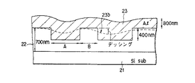
また、被研磨材としての図3に示す試料を用いて、ディッシング量の評価を行った。前記試料は、Si基板21上に凹凸を有するシリコン酸化膜22が形成され、このシリコン酸化膜22の全面にAl膜23が堆積されている。
【0063】
なお、Al膜23の膜厚は800nm、シリコン酸化膜22の膜厚は、700nm、シリコン酸化膜22に形成された凹部の高さは400nmである。また、凹部の幅Aと、凹部の配置間隔Bの関係が、A/(A+B)が0.7になるようにしつつ、凹部の幅Aを10μmと100μmの場合で評価を行った。
【0064】
なお、Al膜23が研磨され、表面が23bまで研磨された際のディッシング量で評価を行った。
【0065】
ディッシング量の評価結果を表2に示す。
【0066】
【表2】
非常に軟らかい研磨布であるポリテックスを用いて研磨を行った場合のディッシング量は、10nmの配線間隔でも160nmあり、100nmの配線間隔Aでは350nm以上もあった。
【0068】
また、コンディショニングが行われた従来の研磨布IC−1000を用いて研磨を行った場合のディッシング量は、80nm(A=10μm),210nm(A=100μm)であり、ポリテックスを用いた場合よりは改善されているが、やはり非常に大きい値である。
【0069】
コンディショニングによりIC−1000の表面層には軟らかい層が形成されて研磨の際に被研磨材の表面層における平坦化性に悪影響を及ぼすため、コンディショニングを行わないで研磨を行ったほうが、ディッシング量が小さくなると考えられる。
【0070】
ところが、結果は逆で、コンディショニングを行わずに研磨を行った場合のディッシング量は、200nm(A=10μm),250nm(A=100μm)であり、コンディショニングを行った場合よりも悪くなっている。
【0071】
これは、コンディショニングを行わないと、Alの表面に深い傷(>200nm)がつき、傷が拡大する形でAlの浸食が進むためである。
【0072】
これらの結果に対し、コンディショニングが行われていない本発明の上記実施形態の研磨布10を用いて研磨を行った場合のディッシング量は、間隔Aが10μmのもので8nm、間隔Aが100μmのもので40nmであり、ディッシングが著しく改善されている。
【0073】
母材自体の圧縮弾性率が10GPaと非常に硬いこと、また表面層の軟らかい層が、被研磨材表面にスクラッチを生じさせず、且つ母材表面がスラリーを十分に保持し、この表面層の軟らかい層の厚さが、非常に薄くなるよう制御されていることのためディッシングの改善がなされた。
【0074】
また、コンディショニング処理が行われた研磨布10を用いて研磨した場合のディッシング量は、20nm(A=10μm),80nm(A=100μm)であった。
【0075】
ディッシング量が悪化したのは、コンディショニングにより、研磨布の表面の軟らかい層がより軟らかくなった為か、軟らかい層が厚くなった為、若しくはその両方のためである。
【0076】
次に、水溶性フィラー12の粒径を変えてAl膜に対する研磨速度の評価を行った。なお、全ての粒径で水溶性フィラーの濃度を25wt%に固定して研磨布を製造した。その結果を表3に示す。
【0077】
【表3】
表3から、水溶性フィラー12の粒径に応じて研磨速度が変化していることが確認された。粒径が1μmの場合、被研磨材であるAl膜の表面に多数のスクラッチが発生していた。
【0079】
これは、研磨布の粒径が小さすぎるため、研磨布の表面に形成される凹凸が微細すぎて、表面に軟らかな層が形成されなかったのと同時に、スラリーの保持が困難であったためである。
【0080】
一方、粒径が50μm及び100μmの場合、研磨速度が遅くなっている。これは、凹凸が大きすぎたためと考えられる。以上の結果から、水溶性フィラーの粒径は、5乃至30μm程度が好ましいと言える。
【0081】
以上説明したように、本実施形態の研磨布は、凹凸が形成され軟らかい表面層と、母材及び固体の水溶性フィラーからなる硬い内部層とから構成されているので、理想的な研磨布にほぼ等しくなる。
【0082】
従って、研磨布の凹凸のある軟らかい表面層によって、研磨速度の向上及び被研磨材の表面層に生ずるスクラッチの形成が抑制されると共に、研磨布の内部の硬い層によって平坦化の向上を図ることができる。
【0083】
また、本発明の研磨布は、母材の表面層が削れても新しい、水溶性フィラーが露出して水又はスラリーに溶け出すので、常に表面層に軟らかい層が存在するので、安定した研磨速度を得ることができる。
【0084】
また、軟らかい表面層が自動的に形成されるので、コンディショニング処理をほとんど必要としないので、研磨布の寿命が長くなる。
【0085】
(第2実施形態)
図4は、本発明の第2実施形態に係わる研磨布の構成を示す断面図である。
【0086】
なお、図4において、図2と同一なものには同一符号を付し、その詳細な説明を省略する。
【0087】
本実施形態の特徴は、水溶性フィラー12の表面が、水(スラリー)に対して不溶性の材料からなるコーティング層31でコーティングされていることである。
【0088】
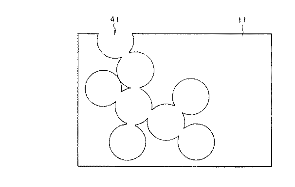
水溶性フィラーを多量に母材中に混入させた場合、水溶性フィラー同士が接触する確率が高くなる。複数の水溶性フィラー同士が接触した状態で、水につけると、図5に示すように、深い凹部41が形成されてしまう。
【0089】
しかし、本実施形態のように、コーティング層でコーティングすることで、接触している水溶性フィラー12が、全て溶けることがない。従って、母材内の奥深くまで凹部が形成されることによる、弾性率の低下を防ぐことができる。
【0090】
なお、本発明は、上記実施形態に限定されるものではない。例えば、上記実施形態では、母材としてポリスチレンを、また水溶性フィラーとしてセルロースを例として挙げたが、他の材料を用いることができる。
【0091】
また、固体の水溶性フィラーの代わりに、液体を母材中に分散混入させても良い。液体は、固体に比べて軟らかいが、気体に比べれば十分硬いので、水溶性フィラーの替わりに用いることができる。もちろん、表面に露出した液体は流れ出るので、液体が存在していた領域に凹部が形成され、固体の水溶性フィラーと同様の効果を持つ。
【0092】
また、母材中に混入される微粒子としては、水溶性だけでなく、他の溶媒に対して溶けるようなもので有ればよい。研磨処理を行う前に、研磨布の表面に微粒子を溶かし得る溶媒を浴びせることによって微粒子を溶かし凹部を形成すればよい。
【0093】
次に、上記研磨布を用いて、配線溝を有するダマシン配線構造の半導体装置を製造する方法の実施態様について説明する。
【0094】
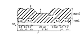
図6は、SiO2基板1に設けられた配線溝2中にAl配線3を埋め込むダマシン配線構造の部分的な断面図を示している。
【0095】
配線溝2の深さは、4,000Å(オングストローム)、幅は、100μm、及び研磨前におけるAl配線3のAl層の厚さを8,000Å(オングストローム)とする。
【0096】
このような構造で、配線溝2にAl配線3を埋め込み、上方からAl配線3の表面を研磨布で研磨したとき、SiO2基板1の表面以下の溝内にまでオーバーポリシング(Over Polishing)してしまい、いわゆるデッシング(Dishing)又は シニング(Thinning)が生じてしまう。
【0097】
この実施態様において、荷重300g/cm2 、テーブル及びキャリアの回転数50rpmで平坦性の評価を行った。その結果、配線溝2に埋め込まれたAl配線3上のスクラッチは、KLAで評価を行ったところ、従来の研磨布IC−1000では、42,328個/Wafer、観察された。
【0098】
これに対し、本発明の研磨布は、320個の/Waferのスクラッチが観察されたに過ぎなかった。
本発明の研磨布において、デッシング(Dishing)の発生が従来の研磨布と比較して格段に改善されたことを図7に示す。
【0099】
従来の研磨布IC−1000を用いてAl配線3を研磨したときに発生するデッシング(Dishing)の数は、点線で示すようにオーバーポリシング(Over Polishing)が溝の深さの60%に至ると3500Dishing(Å)を越えてしまう。
【0100】
これに対して本発明の内部に分散された微粒子を含む研磨布は、Al2O3を3wt%、(NH4)2S2O8を1wt%、及びベンズトリアゾールを0.02%としたスラリーを表面に保持させたものを採用して、Al配線3の表面を研磨したとき、発生するデッシング(Dishing) の数は、実線で示すようにオーバポリシングス(Over Polishing)が溝の深さの60%に達したときであっても、殆ど増加しない。
【0101】
このことは、Al配線3の品質、特性が向上したことを意味し配線形成が良好に行われたと言える。
【0102】
図8は、SiO2基板1に設けられた配線溝2中にCu配線4を埋め込むダマシン配線構造の部分的な断面図を示している。
【0103】
配線溝2の深さは、4,000Å(オングストローム)、幅は、100μm、及び研磨前におけるCu配線4のCu層の厚さを8,000Å(オングストローム)とする。
【0104】
本発明の研磨布において、デッシング(Dishing)の発生が従来の研磨布と比較して格段に改善されたことを図9に示す。
【0105】
従来の研磨布IC−1000を用いてCu配線4を研磨したときに発生するデッシング(Dishing)の数は、点線で示すようにオーバポリシング(Over Polishing)が溝の深さの60%に至ると3500Dishing (Å)の近傍に達する。
【0106】
これに対して、本発明の実施態様の、内部に分散された微粒子を含む研磨布は、Al2O3を1wt%、(NH4)2S2O8を1wt% 及びベンズトリアゾールを0.05%としたスラリーを表面に保持させたものを採用して、Cu配線4の表面を研磨したとき、発生するデッシング(Dishing) の数は、実線で示すようにオーバポリシング(Over Polishing)が溝の深さの60%に達したときであっても、僅かしか増加しない。
【0107】
図10は、SiO2基板1に設けられた配線溝2中にW配線層5を埋め込むダマシン配線構造の部分的な断面図を示している。
【0108】
配線溝2の深さは、4,000Å(オングストローム)、幅は、100μm、及び研磨前におけるW配線層5のW層の厚さを8,000Å(オングストローム)とする。
【0109】
本発明の研磨布において、デッシング(Dishing)の発生が従来の研磨布と比較して格段に改善されたことを図11に示す。
【0110】
従来の研磨布IC−1000を用いてW配線5を研磨したときに発生する
デッシング(Dishing)の数は、点線で示すようにオーバポリシング(Over Polishing)が溝の深さの60%に至ると3500Dishing /Åを越える。
【0111】
これに対して本発明の内部に分散された微粒子を含む研磨布は、Al2O3を3wt%、Fe(NO3)3を5wt% としたスラリーを表面に保持させたものを採用して、W配線5の表面を研磨したとき、発生するデッシング(Dishing)の数は、実線で示すようにオーバポリシング(Over Polishing)が溝の深さの60%に達したときであっても、僅かしか増加しない。
【0112】
次に、本発明の他の実施態様として、図12に示すように、Si基板1上の厚さ14,000Å(オングストローム)の酸化膜6を、深さ7,000Å(オングストローム)、幅が、100μmの配線溝2内に埋設し、本発明の研磨布で酸化膜6を上面から研磨する。このときのスラリーは、Cabot社製SC−1を純水で3倍希釈したものを用いる。
【0113】
その結果、図13に示すように、従来の研磨布IC−1000と本発明の研磨布とを比較したとき、同一のオキサイド・リムーバル(Oxide Removal)量Å(オングストローム)を得るのに、リメイニング・ステップ(Remaining Step)量Å(オングストローム)は、本発明の研磨布の方がより理想的曲線に近付いていることが分かる。
【0114】
それによって、本発明の研磨布を用いて酸化膜の表面を研磨することによって、ばらつきのない平坦化が実現できる。
【0115】
その他、本発明は、その要旨を逸脱しない範囲で、種々変形して実施することが可能である。
【0116】
【発明の効果】
以上説明したように本発明の研磨布によれば、被研磨材の表面を機械的に研磨するための母材中に、溶媒に対して可溶である微粒子を分散混入することによって、特に、研磨中に前記微粒子が前記溶媒に溶けて、研磨布の表面に凹部を形成するので、被研磨材の表面層上において、高い平坦化性能,安定した研磨速度が得られ、被研磨材の表面でのスクラッチの発生を抑制できる。
【0117】
又、基板上に配線溝を設け、この配線溝中に金属配線を埋め込み、前記金属配線の不要部分を、母材中に溶媒に対して可溶である微粒子を分散混入して構成した研磨布で研磨し除去することにより、前記金属配線(特にダマシン配線)のクオリティを高めることができる。
【0118】
更に、この発明の研磨布を用いた半導体の製造方法は、配線溝中に金属配線に替え酸化膜を埋設した場合でも、本発明の研磨布で研磨することにより、前記酸化膜の表面を良好に平坦化できる。
【図面の簡単な説明】
【図1】理想的な研磨布の構成を示す模式図。
【図2】本発明の第1実施形態に係わる研磨布の構成を示す部分的断面図。
【図3】研磨布の評価に用いた被研磨体の構成を部分的に示す断面図。
【図4】本発明の第2の実施形態に係わる研磨布の構成を示す部分的断面図。
【図5】研磨布の微粒子同士が接触することによって生ずる問題点を説明するための研磨布の断面図。
【図6】本発明の研磨布を用いて研磨される埋め込み配線(ダマシン配線)構造の金属配線がAl である場合の半導体装置の形成過程を示す要部断面図。
【図7】本発明の研磨布を用いて図5に示す金属配線Alを研磨したときのデッシング(Dishing)の発生を従来例と比較したときの図。
【図8】本発明の研磨布を用いて研磨される埋め込み配線(ダマシン配線)構造の金属配線がCu である場合の半導体装置の形成過程を示す要部断面図。
【図9】本発明の研磨布を用いて図7に示す金属配線Cuを研磨したときのデッシング(Dishing)の発生を従来例と比較したときの図。
【図10】本発明の研磨布を用いて研磨される埋め込み配線(ダマシン配線)構造の金属配線がW である場合の半導体装置の形成過程を示す要部断面図。
【図11】本発明の研磨布を用いて図9に示す金属配線Wを研磨したときのデッシング(Dishing)の発生を従来例と比較したときの図。
【図12】本発明の半導体装置の製造方法に係る応用例を示し、基板に設けられた溝中に埋め込まれた酸化膜を本発明の研磨布を用いて研磨する半導体装置の形成過程を示す要部断面図。
【図13】本発明の研磨布を用いて図10に示す酸化膜を研磨したときの同一リメイニングステップ(Remaining step)/Åにおいてオキサイド・リムーバル(Oxide Removal)の値が従来例と比較して改善されたことを示す図。
【符号の説明】
10…研磨布
11…母材
12…水溶性フィラー(微粒子)
31…コーティング層
1…SiO2 基板
2…配線溝
3…金属配線Al
4…金属配線Cu
5…金属配線W
6…酸化膜[0001]
BACKGROUND OF THE INVENTION
The present invention relates to a polishing cloth used for chemical mechanical polishing (CMP) and a method for manufacturing a semiconductor device using the polishing cloth.
[0002]
[Prior art]
At present, a chemical mechanical polishing (CMP) method in which an insulating material or a wiring material is polished and its surface is flattened is attracting attention.
There are roughly two types of polishing cloths used for polishing. One is represented by Politex (Rodel) and does not require pad conditioning (dressing).
[0003]
Since Polytex has a cross-sectional structure in which takotsubo are arranged, it has excellent retention of slurry (water, SiO2, Al203, chemicals (oxidant), etc.) used during polishing. Further, the surface is very flexible and does not cause a sharp scratch on the surface of the material to be polished after polishing.
[0004]
However, the compression elastic modulus of this polishing cloth is very soft because it is less than 10 MPa. Therefore, when politex is used in the planarization process of the material to be polished, there is a problem that the polishing rate is very slow and the planarization property is inferior.
[0005]
The other is a cloth represented by IC-1000 (Rodel). Bubbles are formed inside IC-1000, and the compression elastic modulus is about 200 MPa, which is considerably harder than that of Polytex.
[0006]
Normally, the polishing cloth of IC-1000 uses a diamond conditioning plate, and in the case of a semiconductor device, the wafer as the polishing agent is polished one by one for the pad conditioning process, and the surface layer of the polishing cloth of IC-1000 is formed. Scratch to form a soft layer.
[0007]
This is to prevent the polishing rate from being extremely slow because the surface layer is hard and the ratio of the slurry held is reduced unless the conditioning treatment is performed.
[0008]
On the other hand, the life of the polishing cloth of IC-1000 is determined by the number of conditioning processes. This is because the surface layer is scratched by the conditioning treatment.
[0009]
Incidentally, after the conditioning treatment of 1000 wafers as the material to be polished, the surface layer of the polishing cloth is lost by about 850 μm compared to the state before the processing. In order to prolong the service life, when the conditioning conditions are eased so as to reduce the amount of scratching of the surface layer of the polishing cloth, the polishing rate becomes slow or unstable.
[0010]
Further, a soft layer (compression elastic modulus of 10 MPa or less) having a thickness of about several tens of μm is formed on the surface of the polishing pad immediately after conditioning, and this soft layer inhibits flatness.
[0011]
Furthermore, this soft layer is compressed and hardened with the progress of polishing. Therefore, the surface layer of the material to be polished has little scratch immediately after the start of polishing, but the scratch generated on the surface layer of the material to be polished increases when the polishing cloth is compressed and hardened for a long time after polishing. .
[0012]
As described above, the polishing cloth represented by POLITEX has a soft layer, which is the surface layer, and therefore there is a problem that the polishing rate and flatness are inferior although there are few scratches generated on the surface layer of the material to be polished. there were.
[0013]
Further, the polishing cloth represented by IC-1000 has a problem that many scratches are generated on the surface layer of the material to be polished as the polishing time becomes long unless conditioning treatment is performed.
[0014]
On the other hand, when conditioning is performed, the surface of the polishing cloth is scratched and thins, resulting in a short life.
[0015]
Further, when the semiconductor device is polished for forming a buried wiring (damascene wiring), for example, using the above-described conventional polishing cloth, dishing or thinning occurs due to over polishing. .
[0016]
This brings about drawbacks such as short-circuiting the wiring formed in the upper layer in the lithography process, and increasing the resistance due to the length of the wiring becoming wavy.
[0017]
[Problems to be solved by the invention]
The object of the present invention is to eliminate the above-mentioned drawbacks of the conventional polishing cloth, to have a high leveling performance on the material to be polished, to obtain a stable polishing speed, and to suppress the generation of scratches on the surface of the material to be polished. And a method of manufacturing a semiconductor device using the polishing cloth.
[0018]
[Means for Solving the Problems]
In order to achieve the above object, the present invention is configured as follows.
[0019]
The polishing cloth of the present invention (Claim 1) is dispersed in the base material that holds the slurry on the surface and mechanically polishes the surface of the substrate to be processed. water Soluble on the surface and the surface water And fine particles on which a coating layer that is insoluble is formed.
[0020]
At this time, when the surface of the substrate to be processed is mechanically polished on the surface of the base material (Claim 2), the fine particles present on the surface are water A concave portion corresponding to the fine particles is formed by being dissolved in the material.
[0021]
The fine particles (Claim 1) are formed on the surface of the fine particles. water Since the coating layer is insoluble to the inside of the base material, a plurality of fine particles come into contact with each other inside the base material, and all the fine particles in contact with the base material melt, forming a large recess from the surface to the inside, and softening the inside Can be prevented.
[0022]
At this time, the base material (Claim 4) has no voids inside. This is for maintaining the hardness for ensuring flatness when the surface of the material to be polished is polished.
[0024]
The fine particles ( Claim 5 ) Preferably has a particle size of 5 to 30 μm in order to increase the polishing rate.
[0025]
The polishing cloth of the present invention (Claim 3) water Soluble on the surface water When the fine particles formed by forming a coating layer insoluble in the dispersion are dispersed and the surface of the material to be polished is mechanically polished, the slurry is held on the surface, and the fine particles are water And a base material in which concave portions corresponding to the fine particles are formed on the surface. In this case, the fine particles are exposed while the surface layer of the base material gradually decreases during polishing, water As a result, the fine particles are melted and a new recess is formed in the surface layer.
[0026]
At this time, the fine particles (Claim 3) water Since a coating layer that is insoluble in the base material is formed, a plurality of fine particles come into contact with each other inside the base material, and all the fine particles that come into contact melt, forming a large recess from the surface to the inside, and softening the inside. To prevent it.
[0027]
At this time, the base material ( Claim 4 ) Has no voids inside. This is for maintaining the hardness for ensuring flatness when the surface of the material to be polished is polished.
[0029]
The fine particles ( Claim 5 ) Preferably has a particle size of 5 to 30 μm in order to increase the polishing rate.
[0030]
Also, a method of manufacturing a semiconductor device using the polishing cloth of the present invention ( Claim 6 ) Forming an insulating film on the substrate and then providing a wiring groove on the substrate through the insulating film; providing a metal wiring layer on the substrate and the wiring groove; and the metal wiring in the wiring groove A base material that holds the slurry on the surface and mechanically polishes the surface of the material to be polished, and is dispersed in the base material, is soluble in a solvent, and is on the surface. A step of polishing and removing unnecessary portions of the metal wiring embedded in the wiring groove with a polishing cloth comprising fine particles forming a coating layer insoluble in a solvent, and flattening the surface of the metal wiring And including.
[0031]
At this time, the metal wiring is mainly composed of Al ( Claim 7 ) And the main component is Cu ( Claim 8 ) Or the main component is W ( Claim 9 ).
[0032]
Furthermore, a method for manufacturing a semiconductor device using the polishing cloth of the present invention ( Claim 10 ) Providing a groove in the substrate; providing an oxide film on the substrate; embedding the oxide film in the groove; and holding the slurry on the surface and mechanically polishing the surface of the material to be polished. A polishing cloth comprising a base material to be polished and fine particles that are dispersed in the base material and have a coating layer that is soluble in a solvent and insoluble in the solvent on the surface thereof. Polishing and removing unnecessary portions of the oxide film buried in the substrate, and planarizing the surface of the oxide film.
[0033]
At this time, the oxide film ( Claim 11 ) Is preferably SiO 2 It is.
[0034]
DETAILED DESCRIPTION OF THE INVENTION
Before describing the embodiment of the present invention, the configuration of an ideal polishing cloth in terms of performance will be described with reference to FIG.
[0035]
A polishing cloth as shown in FIG. 13 is conceivable in order to satisfy the conditions of stable polishing speed, high planarization performance of the surface of the material to be polished, suppression of generation of scratches and long life.
[0036]
The
[0037]
The polishing cloth of the present invention has all the above conditions. The inside of the polishing cloth has a hard structure because fine particles are dispersed in the base material. Further, unlike the conventional polishing cloth IC-1000, since there is no hole, it is hard.
[0038]
Further, the surface layer of the polishing cloth has water-soluble fine particles exposed on the surface dissolved in a solvent to form a concave portion. Therefore, the surface layer is widened by forming irregularities on the surface, and the slurry retainability is good.
[0039]
Further, when the surface is uneven, the surface becomes softer than the inside, so that the generation of scratches is suppressed.
[0040]
In another embodiment of the present invention, when the surface of the fine particles is coated, even if a plurality of fine particles are in contact with each other, all of the fine particles in contact are not melted.
[0041]
When all the fine particles that come in contact melt, a large recess is formed and the inner layer becomes soft, but by coating the surface, only the fine particles exposed on the surface are soluble in the solvent, Since the fine particles are not melted, a large concave portion is not formed.
[0042]
When the solvent is water or slurry, even if the surface is scraped during the polishing step, the newly exposed fine particles are dissolved into the water or slurry, so that there is little deterioration in performance during polishing.
[0043]
Further, when the particle size of the fine particles is 5 to 30 μm, the polishing rate is fast.
[0044]
More specifically, an embodiment of the present invention will be described with reference to FIG.
[0045]
[First Embodiment]
FIG. 2 is a cross-sectional view showing the structure of the CMP polishing cloth according to the first embodiment of the present invention. In this polishing
[0046]
Since the base material 11 is hard and the water-
[0047]
When the water-
[0048]
In addition, since the soft surface layer changes the density and thickness of the concave portions formed on the surface by controlling the particle size and mixing ratio of the water-soluble filler, the thickness can be easily controlled. Is possible. Therefore, it is possible to easily control the softness and thickness of the surface layer by controlling the particle size and mixing rate of the water-soluble filler.
[0049]
Table 1 shows the polishing rate and the occurrence of scratches when polishing an Al material containing 0.5% Cu using the polishing
[0050]
[Table 1]
In the case of the conventional polishing cloth IC-1000, if the conditioning process is not performed, the polishing rate is 60 nm / min, which is extremely slow compared to the polishing rate 210 nm / min when the conditioning process is performed.
[0052]
The reason why the polishing rate without the conditioning treatment is low is considered to be because the slurry is not retained on the surface layer of the polishing pad.
[0053]
On the other hand, the polishing cloth of this embodiment has a large polishing rate of 205 nm / min even without conditioning treatment. This is because the water-soluble filler exposed on the surface of the polishing cloth is dissolved in water (slurry), and the area where the water-soluble filler was present becomes a concave portion and the surface area is increased, so that the retention of the slurry is improved. .
[0054]
The reason why the polishing rate without the conditioning treatment is low is considered to be because the slurry is not retained in the surface layer.
[0055]
On the other hand, the polishing cloth of this embodiment has a large polishing rate of 205 nm / min even without conditioning treatment. This is because the water-soluble filler exposed on the surface of the polishing cloth is dissolved in water (slurry), and the area where the water-soluble filler was present becomes a concave portion and the surface area is increased, so that the retention of the slurry is improved. .
[0056]
The reason why the polishing rate without the conditioning treatment is low is considered to be because the slurry is not retained in the surface layer.
[0057]
On the other hand, the polishing cloth of this embodiment has a large polishing rate of 205 nm / min even without conditioning treatment. This is because the water-soluble filler exposed on the surface of the polishing cloth is dissolved in water (slurry), and the area where the water-soluble filler was present becomes a concave portion and the surface area is increased, so that the retention of the slurry is improved. .
[0058]
The reason why the polishing rate without the conditioning treatment is low is considered to be because the slurry is not retained on the surface layer of the polishing pad.
[0059]
On the other hand, the polishing cloth of this embodiment has a large polishing rate of 205 nm / min even without conditioning treatment. This is because the water-soluble filler exposed on the surface of the polishing cloth is dissolved in water (slurry), and the area where the water-soluble filler was present becomes a concave portion and the surface area is increased, so that the retention of the slurry is improved. .
[0060]
In addition, the polishing cloth of this embodiment was obtained with a stable polishing rate. This is because the water-
[0061]
Further, when the
[0062]
In addition, the dishing amount was evaluated using the sample shown in FIG. 3 as the material to be polished. In the sample, a
[0063]
The film thickness of the
[0064]
The evaluation was performed using the dishing amount when the
[0065]
Table 2 shows the evaluation results of the dishing amount.
[0066]
[Table 2]
The amount of dishing when polishing using a politex, which is a very soft polishing cloth, was 160 nm even at a wiring interval of 10 nm, and 350 nm or more at a wiring interval A of 100 nm.
[0068]
In addition, the amount of dishing when polishing is performed using a conventional polishing cloth IC-1000 that has been conditioned is 80 nm (A = 10 μm) and 210 nm (A = 100 μm), which is greater than when using a tex. Is improved, but still very large.
[0069]
Since a soft layer is formed on the surface layer of the IC-1000 by conditioning and adversely affects the flatness of the surface layer of the material to be polished during polishing, the amount of dishing is better when polishing is performed without conditioning. It will be smaller.
[0070]
However, the results are opposite, and the dishing amounts when polishing is performed without conditioning are 200 nm (A = 10 μm) and 250 nm (A = 100 μm), which are worse than those obtained when conditioning is performed.
[0071]
This is because if conditioning is not performed, deep scratches (> 200 nm) are formed on the surface of Al, and Al erosion proceeds in such a manner that the scratches expand.
[0072]
In response to these results, the dishing amount when polishing was performed using the polishing
[0073]
The compression modulus of the base material itself is very hard as 10 GPa, and the soft layer of the surface layer does not cause scratches on the surface of the material to be polished, and the base material surface sufficiently holds the slurry. The dishing was improved because the thickness of the soft layer was controlled to be very thin.
[0074]
Moreover, the dishing amount at the time of grinding | polishing using the polishing
[0075]
The dishing amount deteriorated because the softening layer on the surface of the polishing cloth became softer, the softening layer became thicker, or both.
[0076]
Next, the polishing rate for the Al film was evaluated by changing the particle size of the water-
[0077]
[Table 3]
From Table 3, it was confirmed that the polishing rate was changed according to the particle size of the water-
[0079]
This is because the particle size of the polishing cloth was too small, the irregularities formed on the surface of the polishing cloth were too fine, and a soft layer was not formed on the surface, and at the same time it was difficult to hold the slurry. is there.
[0080]
On the other hand, when the particle size is 50 μm and 100 μm, the polishing rate is slow. This is probably because the irregularities were too large. From the above results, it can be said that the particle size of the water-soluble filler is preferably about 5 to 30 μm.
[0081]
As described above, the polishing cloth of this embodiment is composed of a soft surface layer with irregularities formed thereon and a hard inner layer made of a base material and a solid water-soluble filler. Almost equal.
[0082]
Therefore, the soft surface layer with unevenness of the polishing cloth suppresses the improvement of the polishing rate and the formation of scratches on the surface layer of the material to be polished, and the flattening is improved by the hard layer inside the polishing cloth. Can do.
[0083]
In addition, the polishing cloth of the present invention has a stable polishing rate since a new water-soluble filler is exposed and dissolves in water or slurry even if the surface layer of the base material is scraped, and a soft layer always exists in the surface layer. Can be obtained.
[0084]
In addition, since the soft surface layer is automatically formed, almost no conditioning treatment is required, so the life of the polishing cloth is prolonged.
[0085]
(Second Embodiment)
FIG. 4 is a cross-sectional view showing the configuration of the polishing pad according to the second embodiment of the present invention.
[0086]
4 that are the same as those in FIG. 2 are assigned the same reference numerals, and detailed descriptions thereof are omitted.
[0087]
The feature of this embodiment is that the surface of the water-
[0088]
When a large amount of water-soluble filler is mixed in the base material, the probability that the water-soluble fillers come into contact with each other increases. If the water-soluble fillers are in contact with each other and put on water, deep recesses 41 are formed as shown in FIG.
[0089]
However, as in this embodiment, the water-
[0090]
The present invention is not limited to the above embodiment. For example, in the above embodiment, polystyrene is used as an example of the base material and cellulose is used as an example of the water-soluble filler. However, other materials can be used.
[0091]
Further, instead of the solid water-soluble filler, a liquid may be dispersed and mixed in the base material. The liquid is softer than the solid, but is sufficiently harder than the gas, and can be used instead of the water-soluble filler. Of course, since the liquid exposed on the surface flows out, a recess is formed in the area where the liquid was present, and the effect is similar to that of a solid water-soluble filler.
[0092]
Further, the fine particles mixed in the base material need only be soluble in other solvents as well as water-soluble. Before performing the polishing treatment, the concave portions may be formed by dissolving the fine particles by exposing the surface of the polishing cloth to a solvent capable of dissolving the fine particles.
[0093]
Next, an embodiment of a method for manufacturing a semiconductor device having a damascene wiring structure having a wiring groove using the polishing cloth will be described.
[0094]
FIG. 6 shows SiO 2 A partial cross-sectional view of a damascene wiring structure in which an
[0095]
The depth of the
[0096]
With such a structure, when the
[0097]
In this embodiment, the load is 300 g / cm. 2 The flatness of the table and carrier was evaluated at 50 rpm. As a result, scratches on the
[0098]
On the other hand, in the polishing cloth of the present invention, only 320 / Wafer scratches were observed.
FIG. 7 shows that the occurrence of dishing in the polishing cloth of the present invention is remarkably improved as compared with the conventional polishing cloth.
[0099]
The number of dishing that occurs when the
[0100]
On the other hand, the polishing cloth containing fine particles dispersed inside the present invention is made of Al. 2
[0101]
This means that the quality and characteristics of the
[0102]
FIG. 8 shows SiO 2 A partial sectional view of a damascene wiring structure in which a
[0103]
The depth of the
[0104]
FIG. 9 shows that the occurrence of dishing in the polishing cloth of the present invention is remarkably improved as compared with the conventional polishing cloth.
[0105]
The number of dishing that occurs when the
[0106]
On the other hand, the polishing cloth containing fine particles dispersed in the embodiment of the present invention is Al. 2
[0107]
FIG. 10 shows SiO 2 A partial cross-sectional view of a damascene wiring structure in which a
[0108]
The depth of the
[0109]
FIG. 11 shows that the occurrence of dishing in the polishing cloth of the present invention is remarkably improved as compared with the conventional polishing cloth.
[0110]
Occurs when the
As indicated by the dotted line, the number of dishing exceeds 3500 Dishing / Å when over polishing reaches 60% of the groove depth.
[0111]
On the other hand, the polishing cloth containing fine particles dispersed inside the present invention is made of Al. 2
[0112]
Next, as another embodiment of the present invention, as shown in FIG. 12, an
[0113]
As a result, as shown in FIG. 13, when the conventional polishing cloth IC-1000 is compared with the polishing cloth of the present invention, the same Oxide Removal amount angstrom is obtained. It can be seen that the Remaining Step amount Å is closer to the ideal curve for the polishing cloth of the present invention.
[0114]
Thereby, flattening without variation can be realized by polishing the surface of the oxide film using the polishing cloth of the present invention.
[0115]
In addition, the present invention can be variously modified and implemented without departing from the scope of the invention.
[0116]
【The invention's effect】
As described above, according to the polishing cloth of the present invention, by dispersing and mixing fine particles soluble in a solvent into a base material for mechanically polishing the surface of a material to be polished, Since the fine particles dissolve in the solvent during polishing and form a recess on the surface of the polishing cloth, high planarization performance and a stable polishing speed are obtained on the surface layer of the material to be polished, and the surface of the material to be polished It is possible to suppress the occurrence of scratches in
[0117]
Also, a polishing cloth provided with a wiring groove on the substrate, metal wiring embedded in the wiring groove, and unnecessary portions of the metal wiring dispersed and mixed with fine particles soluble in a solvent in the base material The quality of the metal wiring (particularly, damascene wiring) can be improved by polishing and removing with.
[0118]
Furthermore, the semiconductor manufacturing method using the polishing cloth of the present invention provides a good surface of the oxide film by polishing with the polishing cloth of the present invention even when an oxide film is buried in the wiring groove instead of the metal wiring. Can be flattened.
[Brief description of the drawings]
FIG. 1 is a schematic diagram showing a configuration of an ideal polishing cloth.
FIG. 2 is a partial cross-sectional view showing a configuration of a polishing cloth according to the first embodiment of the present invention.
FIG. 3 is a cross-sectional view partially showing a configuration of an object to be polished used for evaluation of a polishing cloth.
FIG. 4 is a partial cross-sectional view showing a configuration of a polishing cloth according to a second embodiment of the present invention.
FIG. 5 is a cross-sectional view of a polishing cloth for explaining a problem caused by contact between fine particles of the polishing cloth.
FIG. 6 is a fragmentary cross-sectional view showing the process of forming a semiconductor device when the metal wiring of the embedded wiring (damascene wiring) structure polished using the polishing cloth of the present invention is Al.
7 is a diagram when the occurrence of dishing when the metal wiring Al shown in FIG. 5 is polished using the polishing cloth of the present invention is compared with a conventional example.
FIG. 8 is a fragmentary cross-sectional view showing the process of forming a semiconductor device when the metal wiring of the embedded wiring (damascene wiring) structure polished using the polishing cloth of the present invention is Cu.
FIG. 9 is a view when the occurrence of dishing when the metal wiring Cu shown in FIG. 7 is polished using the polishing cloth of the present invention is compared with the conventional example.
FIG. 10 is a fragmentary cross-sectional view showing the process of forming a semiconductor device when the metal wiring of the embedded wiring (damascene wiring) structure polished using the polishing cloth of the present invention is W.
11 is a diagram in which the occurrence of dishing when the metal wiring W shown in FIG. 9 is polished using the polishing cloth of the present invention is compared with a conventional example.
FIG. 12 shows an application example related to a method for manufacturing a semiconductor device of the present invention, and shows a process of forming a semiconductor device for polishing an oxide film embedded in a groove provided in a substrate using the polishing cloth of the present invention. FIG.
FIG. 13 shows the value of Oxide Removal compared with the conventional example in the same remaining step / reduction when the oxide film shown in FIG. 10 is polished using the polishing cloth of the present invention. The figure which shows having improved.
[Explanation of symbols]
10 ... Polishing cloth
11 ... Base material
12 ... Water-soluble filler (fine particles)
31 ... Coating layer
1 ... SiO 2 substrate
2. Wiring groove
3 ... Metal wiring Al
4 ... Metal wiring Cu
5 ... Metal wiring W
6 ... Oxide film
Claims (11)
前記母材中に分散され、水に対して可溶であり、且つその表面に前記水に対して不溶であるコーティング層が形成されている微粒子と、より成ることを特徴とする研磨布。A base material that holds the slurry on the surface and mechanically polishes the surface of the substrate to be treated;
A polishing cloth comprising fine particles dispersed in the base material, soluble in water and having a coating layer formed on the surface thereof insoluble in water .
内部に前記微粒子が分散され、被研磨材の表面を機械的に研磨する際、その表面にスラリーを保持し、且つその表面に存在する前記微粒子が前記水に溶けて前記表面に微粒子に対応する凹部が形成される母材と、より成ることを特徴とする研磨布。Soluble in water, and a particulate coating layer is formed is insoluble in the water on its surface,
When the fine particles are dispersed inside and the surface of the material to be polished is mechanically polished, the slurry is held on the surface, and the fine particles present on the surface dissolve in the water and correspond to the fine particles on the surface. A polishing cloth comprising a base material on which a recess is formed.
前記基板及び前記配線溝上に金属配線層を設ける工程と、
前記配線溝中に金属配線を埋設する工程と、
表面でスラリーを保持し且つ被研磨材の表面を機械的に研磨する母材と、前記母材中に分散され、溶媒に対して可溶であり且つその表面に前記溶媒に対して不溶であるコーティング層が形成されている微粒子とより成る研磨布によって、前記配線溝中に埋設された金属配線の不要部分を研磨し除去し、前記金属配線の表面を平坦化する工程と、を含むことを特徴とする研磨布を用いた半導体装置の製造方法。Forming an insulating film on the substrate, and then providing a wiring groove in the substrate through the insulating film;
Providing a metal wiring layer on the substrate and the wiring groove;
Burying metal wiring in the wiring groove;
A base material that holds the slurry on the surface and mechanically polishes the surface of the material to be polished, and is dispersed in the base material, is soluble in a solvent, and is insoluble in the solvent on the surface Polishing and removing unnecessary portions of the metal wiring embedded in the wiring groove with a polishing cloth made of fine particles on which a coating layer is formed, and planarizing the surface of the metal wiring. A method for manufacturing a semiconductor device using a polishing cloth.
前記基板上に酸化膜を設け、前記溝内に前記酸化膜を埋設する工程と、
表面でスラリーを保持し、且つ被研磨材の表面を機械的に研磨する母材と、前記母材中に分散され、溶媒に対して可溶であり、且つその表面に前記溶媒に対して不溶であるコーティング層が形成されている微粒子とより成る研磨布によって、前記溝中に埋設された酸化膜の不要部分を研磨し除去し、前記酸化膜の表面を平坦化する工程と、を含むことを特徴とする研磨布を用いた半導体装置の製造方法。Providing a groove in the substrate;
Providing an oxide film on the substrate, and burying the oxide film in the groove;
A base material that holds the slurry on the surface and mechanically polishes the surface of the material to be polished, and is dispersed in the base material, is soluble in a solvent, and is insoluble in the solvent on the surface. Polishing and removing unnecessary portions of the oxide film embedded in the groove with a polishing cloth made of fine particles on which the coating layer is formed, and planarizing the surface of the oxide film. A manufacturing method of a semiconductor device using a polishing cloth characterized by the above.
Priority Applications (1)
| Application Number | Priority Date | Filing Date | Title |
|---|---|---|---|
| JP11811399A JP3668046B2 (en) | 1998-05-11 | 1999-04-26 | Polishing cloth and method for manufacturing semiconductor device using the polishing cloth |
Applications Claiming Priority (3)
| Application Number | Priority Date | Filing Date | Title |
|---|---|---|---|
| JP10-127441 | 1998-05-11 | ||
| JP12744198 | 1998-05-11 | ||
| JP11811399A JP3668046B2 (en) | 1998-05-11 | 1999-04-26 | Polishing cloth and method for manufacturing semiconductor device using the polishing cloth |
Publications (2)
| Publication Number | Publication Date |
|---|---|
| JP2000033552A JP2000033552A (en) | 2000-02-02 |
| JP3668046B2 true JP3668046B2 (en) | 2005-07-06 |
Family
ID=26456105
Family Applications (1)
| Application Number | Title | Priority Date | Filing Date |
|---|---|---|---|
| JP11811399A Expired - Fee Related JP3668046B2 (en) | 1998-05-11 | 1999-04-26 | Polishing cloth and method for manufacturing semiconductor device using the polishing cloth |
Country Status (1)
| Country | Link |
|---|---|
| JP (1) | JP3668046B2 (en) |
Families Citing this family (16)
| Publication number | Priority date | Publication date | Assignee | Title |
|---|---|---|---|---|
| US6953388B2 (en) | 1999-12-22 | 2005-10-11 | Toray Industries, Inc. | Polishing pad, and method and apparatus for polishing |
| JP3925041B2 (en) | 2000-05-31 | 2007-06-06 | Jsr株式会社 | Polishing pad composition and polishing pad using the same |
| JP2002190460A (en) * | 2000-10-12 | 2002-07-05 | Toshiba Corp | Polishing cloth, polishing apparatus, and method of manufacturing semiconductor device |
| US6685540B2 (en) * | 2001-11-27 | 2004-02-03 | Cabot Microelectronics Corporation | Polishing pad comprising particles with a solid core and polymeric shell |
| JP4039214B2 (en) | 2002-11-05 | 2008-01-30 | Jsr株式会社 | Polishing pad |
| US20040224622A1 (en) | 2003-04-15 | 2004-11-11 | Jsr Corporation | Polishing pad and production method thereof |
| JP4292025B2 (en) | 2003-05-23 | 2009-07-08 | Jsr株式会社 | Polishing pad |
| JP4877448B2 (en) * | 2003-11-04 | 2012-02-15 | Jsr株式会社 | Chemical mechanical polishing pad |
| US7442116B2 (en) | 2003-11-04 | 2008-10-28 | Jsr Corporation | Chemical mechanical polishing pad |
| KR100640141B1 (en) | 2004-04-21 | 2006-10-31 | 제이에스알 가부시끼가이샤 | Chemical mechanical polishing pad, manufacturing process thereof and chemical mechanical polishing method |
| DE602005007125D1 (en) | 2004-09-17 | 2008-07-10 | Jsr Corp | Chemical-mechanical polishing pad and chemical-mechanical polishing process |
| JP4475404B2 (en) | 2004-10-14 | 2010-06-09 | Jsr株式会社 | Polishing pad |
| KR100804275B1 (en) * | 2006-07-24 | 2008-02-18 | 에스케이씨 주식회사 | CPM polishing pad comprising a liquid organic core surrounded by a polymer shell and a method of manufacturing the same |
| JP2009255271A (en) * | 2007-08-01 | 2009-11-05 | Toray Ind Inc | Polishing pad and its manufacturing method |
| US7635290B2 (en) * | 2007-08-15 | 2009-12-22 | Rohm And Haas Electronic Materials Cmp Holdings, Inc. | Interpenetrating network for chemical mechanical polishing |
| CN102284916A (en) * | 2011-07-04 | 2011-12-21 | 南京航空航天大学 | Grinding and polishing pad with composite chip removal structure |
-
1999
- 1999-04-26 JP JP11811399A patent/JP3668046B2/en not_active Expired - Fee Related
Also Published As
| Publication number | Publication date |
|---|---|
| JP2000033552A (en) | 2000-02-02 |
Similar Documents
| Publication | Publication Date | Title |
|---|---|---|
| JP6030703B2 (en) | Use of CsOH in dielectric CMP slurry | |
| JP3668046B2 (en) | Polishing cloth and method for manufacturing semiconductor device using the polishing cloth | |
| US6376381B1 (en) | Planarizing solutions, planarizing machines, and methods for mechanical and/or chemical-mechanical planarization of microelectronic substrate assemblies | |
| CN1292460C (en) | Slurry for CMP, polishing method and method of manufacturing semiconductor device | |
| US20020197935A1 (en) | Method of polishing a substrate | |
| JP2003530713A (en) | Priority removal system for silicon oxide | |
| KR20030036740A (en) | Slurry for use with fixed-abrasive polishing pads in polishing semiconductor device conductive structures that include copper and tungsten and polishing methods | |
| KR100578596B1 (en) | Slurry composition for chemical mechanical polishing, method of planarizing surface of semiconductor device using the same and method of controlling selectivity of slurry composition | |
| JP3895949B2 (en) | CMP slurry and method for manufacturing semiconductor device using the same | |
| EP1292971A2 (en) | Ceria slurry and process for the chemical-mechanical polishing of silicon dioxide | |
| TWI629324B (en) | Method of grinding a substrate | |
| TW202104524A (en) | Chemical mechanical polishing compositions and methods having enhanced defect inhibition and selectively polishing silcon nitiride over silicon dioxide in an acid environment | |
| US5752875A (en) | Method of chemically-mechanically polishing an electronic component | |
| US6337280B1 (en) | Polishing cloth and method of manufacturing semiconductor device using the same | |
| JP2007157841A (en) | Aqueous dispersion for CMP, polishing method, and method for manufacturing semiconductor device | |
| US20040127045A1 (en) | Chemical mechanical planarization of wafers or films using fixed polishing pads and a nanoparticle composition | |
| JP5319887B2 (en) | Slurry for polishing | |
| JP4202955B2 (en) | Chemical mechanical polishing method of organic film | |
| KR102896433B1 (en) | Slurry composition for polishing copper of through silicon via comprising a plate-shaped nanomaterial of multiple size | |
| JP2004523123A (en) | Methods and compositions for CMP polishing | |
| JP2005311011A (en) | Polishing composition | |
| JP2003347244A (en) | Method of polishing semiconductor wafer | |
| JP2007123759A (en) | Semiconductor polishing composition and polishing method | |
| JP2005306977A (en) | Polishing composition | |
| See et al. | 1, 2,* K. Goh,'F. Chen,'S Balakumar, 2G. Higelin |
Legal Events
| Date | Code | Title | Description |
|---|---|---|---|
| A131 | Notification of reasons for refusal |
Free format text: JAPANESE INTERMEDIATE CODE: A131 Effective date: 20041109 |
|
| A521 | Written amendment |
Free format text: JAPANESE INTERMEDIATE CODE: A523 Effective date: 20041203 |
|
| A02 | Decision of refusal |
Free format text: JAPANESE INTERMEDIATE CODE: A02 Effective date: 20050104 |
|
| A521 | Written amendment |
Free format text: JAPANESE INTERMEDIATE CODE: A523 Effective date: 20050304 |
|
| A911 | Transfer of reconsideration by examiner before appeal (zenchi) |
Free format text: JAPANESE INTERMEDIATE CODE: A911 Effective date: 20050309 |
|
| TRDD | Decision of grant or rejection written | ||
| A01 | Written decision to grant a patent or to grant a registration (utility model) |
Free format text: JAPANESE INTERMEDIATE CODE: A01 Effective date: 20050405 |
|
| A61 | First payment of annual fees (during grant procedure) |
Free format text: JAPANESE INTERMEDIATE CODE: A61 Effective date: 20050407 |
|
| FPAY | Renewal fee payment (event date is renewal date of database) |
Free format text: PAYMENT UNTIL: 20080415 Year of fee payment: 3 |
|
| FPAY | Renewal fee payment (event date is renewal date of database) |
Free format text: PAYMENT UNTIL: 20090415 Year of fee payment: 4 |
|
| FPAY | Renewal fee payment (event date is renewal date of database) |
Free format text: PAYMENT UNTIL: 20100415 Year of fee payment: 5 |
|
| FPAY | Renewal fee payment (event date is renewal date of database) |
Free format text: PAYMENT UNTIL: 20100415 Year of fee payment: 5 |
|
| FPAY | Renewal fee payment (event date is renewal date of database) |
Free format text: PAYMENT UNTIL: 20110415 Year of fee payment: 6 |
|
| FPAY | Renewal fee payment (event date is renewal date of database) |
Free format text: PAYMENT UNTIL: 20130415 Year of fee payment: 8 |
|
| LAPS | Cancellation because of no payment of annual fees |