JP3668024B2 - Network interface module - Google Patents
Network interface module Download PDFInfo
- Publication number
- JP3668024B2 JP3668024B2 JP34140598A JP34140598A JP3668024B2 JP 3668024 B2 JP3668024 B2 JP 3668024B2 JP 34140598 A JP34140598 A JP 34140598A JP 34140598 A JP34140598 A JP 34140598A JP 3668024 B2 JP3668024 B2 JP 3668024B2
- Authority
- JP
- Japan
- Prior art keywords
- signal
- circuit
- channel
- analog
- output
- Prior art date
- Legal status (The legal status is an assumption and is not a legal conclusion. Google has not performed a legal analysis and makes no representation as to the accuracy of the status listed.)
- Expired - Fee Related
Links
Images
Landscapes
- Two-Way Televisions, Distribution Of Moving Picture Or The Like (AREA)
Description
【0001】
【発明の属する技術分野】
この発明はCATV(ケーブルテレビジョンの略)向けのケーブルモデムまたはSTB(セットトップボックスの略)に好適に使用されるNIM(ネットワークインターフェイスモジュールの略)に関し、特に、回路構成が改善されるNIMに関する。
【0002】
【従来の技術】
CATVの事業者は、多チャンネル化や、空きチャンネルを利用した広帯域データ通信サービスなどの提供のために、家庭の引込み線が同軸ケーブルであって、幹線ネットワークを光ファイバ化したHFC(Hybrid Fiber Coax )の導入を進めている。これによって、たとえば64値のQAM(直交位相変調)を用いることによって、1チャンネルの帯域幅6MHzで、伝送速度30Mビット/秒の高速データラインを作成できる。このようなCATV用のケーブルモデムまたはSTB内には、ケーブルネットワークと家庭側とを通信接続するためにNIMが搭載される。
【0003】
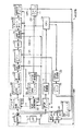
図8は、従来のSTB40Aのブロック構成図である。
図8ではSTB40Aは図示されないケーブル回線を介して図示されないCATV局と該STB40Aとを接続するために入力端子1を含む。
【0004】
入力端子1からケーブル回線を介してCATV局に送信される信号は上り信号と呼び、CATV局側からケーブル回線を介して入力端子1に送信される信号は下り信号と呼ぶ。CATVでは、たとえば上り信号は5〜42MHzにて運用され下り信号は54〜860MHzにて運用される。
【0005】
STB40AはNIM1、ビットストリームから映像および音声の信号を取出すトランスポートデコーダ15、MPEG2デコーダ16、マルチプレクサ17、RF(高周波の略)モジュレータ18、CPU19、QPSK(quadrature
phase shift keying)変調器20、パワーアンプ21および出力端子23を含む。
【0006】
NIM1は、入力端子1、HPF(ハイパスフィルタの略)、LPF(ローパスフィルタの略)4、方向性結合器5、デジタルチューナ6、アナログチューナ7、QPSKチューナ8、デジタルSAWフィルタ9、NTSC( national
television system committee )復調器10、QPSK復調器11、ダウンコンバータ12、ADC(アナログ/デジタルコンバータの略)13、QAM復調器14、2分配器22、データ端子26、両側隣接トラップ回路32、アナログSAWフィルタ33およびIF(中間周波の略)増幅器34を含む。
【0007】
上り信号はQPSK変調器20により直交位相偏位変調(QPSK)されたデータ信号としてパワーアンプ21により増幅された後にデータ端子26に与えられる。データ端子26へ与えられたデータ信号はアップストリーム回路であるLPF4および入力端子1を介してケーブル回線に送出される。
【0008】
チューナ6〜8のぞれぞれは470〜860MHzを受信するUHFバンド(B3バンド)、170MHz〜470MHzを受信するVHF Highバンド(B2バンド)、54〜170MHzを受信するVHF Lowバンド(B1バンド)に分割され、各バンドごとの受信回路からなる。ただし、バンド分割はこれに特定されない。
【0009】
下り信号は、入力端子1とIFフィルタであるHPF3を通過の後、方向性結合器5にてチューナ6および2分配器22へ分配して供給される。2分配器22へ与えられる下り信号は分配されてアナログ信号受信用のアナログチューナ7およびQPSK信号受信用のQPSKチューナ8に与えられる。
【0010】
近年のCATV信号の種類はQPSK変調された上り信号および下り信号、アナログのNTSC映像信号およびデジタルのQAM映像信号に分かれる。図8のCATV信号受信用STB40Aではこれらの各信号の送受信を行ない双方向にて処理される。
【0011】
アナログのNTSC映像信号はアナログ映像信号受信回路(回路7〜10)にて、デジタルのQAM映像信号はQAM信号受信回路(回路6、9、12、13、14、15および16)にて処理される。次に、下り信号であるQPSK変調されたデータ信号はQPSK信号受信回路(回路8と11)にて処理され、また上りのQPSK変調されたデータ信号はQPSK信号送信回路(回路20と21)にて処理される。
【0012】
まず、下りのアナログ信号であるNTSC映像信号は入力端子1、HPF3および方向性結合器5および2分配器22を通過の後、アナログチューナ7に与えられて、ここで選局が所望されるアナログチャンネル(アナログ放送受信用チャンネル)に対応のIF信号に変換されて、両側隣接トラップ回路32、IF増幅器34およびアナログSAWフィルタ33を介してNTSC復調器10にて映像信号および音声信号であるコンポジット信号CP1に変換されマルチプレクサ17に出力される。
【0013】
一方、QAM変調されたデジタル信号は方向性結合器5を通過した後、デジタルチューナ6にて選局が所望されるデジタルチャンネル(デジタル放送受信用チャンネル)に対応のIF信号に変換されデジタルSAWフィルタ9を通過しダウンコンバータ12にて低周波のIF信号に変換された後、ADC13にて8ビットまたは10ビットのデジタル信号に変換される。
【0014】
このデジタル信号はQAM復調器14にてI、Q復調され誤り訂正された後、直列ビットストリームとしてトランスポートデコーダ15に出力される。
【0015】
トランスポートデコーダ15は入力した直列ビットストリームからなる映像および音声信号を取出してMPEG2デコーダ16に出力する。MPEG2デコーダ16は入力された映像および音声信号を帯域伸長してアナログのコンポジット信号CP2としてマルチプレクサ17に出力する。
【0016】
マルチプレクサ17は与えられる2つのコンポジット信号CP1およびCP2のいずれか一方をCPU19の指示に従い選択してRFモジュレータ18に出力する。RFモジュレータ18においては、与えられたコンポジット信号は所望されるチャンネルのTV信号に変調されて出力端子23からTV受像機のアンテナ入力端子(図示せず)へ出力される。
【0017】
次に、CATV局であるセンター側と加入者側のSTB40Aとの通信のため、上り信号および下り信号にはQPSK変調信号が用いられる。まず、下りのQPSK変調されせたデータ信号は入力端子1、HPF3および方向性結合器5ならびに2信号分配器22を通過した後にQPSKチューナ8にて選局されて、選局されたデータ信号はQPSK復調器11によりQPSK復調されCPU19に転送される。
【0018】
課金情報などの上りデータ信号はCPU19からQPSK変調器20に与えられて、ここで変調された後、パワーアンプ21にて増幅された後、LPF4を介して入力端子1からケーブル回線に送出される。
【0019】
【発明が解決しようとする課題】
CATV向けのSTBまたはケーブルモデムは小型化が要求されるので、これに搭載されるNIMもRFモジュールとして小型化が要求される。
【0020】
しかしながら、図8に示された従来のNIMをそのままモジュール化したのでは大型となってしまい、NIMが搭載されるSTBまたはケーブルモデムの小型化も阻害される。
【0021】
それゆえにこの発明の目的は、構成が簡単化されて小型化が図られるネットワークインターフェイスモジュールを提供することである。
【0022】
【課題を解決するための手段】
請求項1に記載のネットワークインターフェイスモジュールは、CATV局とケーブル回線を介して信号を送受信するためのものであって、以下の特徴を有する。
【0023】
つまり、信号送受信の端子を介してケーブル回線にCATV局への上りデータ信号を送出するためのローパスフィルタと、ローパスフィルタとは異なる通過帯域を有しCATV局からのアナログ放送用の信号、デジタル放送用の信号および下りデータ信号を含む下り信号を前述の端子を介してケーブル回線から導入するためのハイパスフィルタと、ハイパスフィルタにより導入された下り信号を受信するための受信回路とを、少なくとも備える。
【0024】
そして、受信回路は、以下の特徴を有する。つまり、下り信号を入力して復調して下りデータ信号を出力するデータ復調回路と、下り信号を入力して所定利得で増幅した後にアナログ放送用およびデジタル放送用いずれかの所望チャンネルの中間周波信号に変換して出力する1つのチューナと、ハイパスフィルタにより導入された下り信号を入力してデータ復調回路とチューナに分岐して出力する分岐部と、チューナから出力される所望チャンネルの中間周波信号を入力して、帯域制限しながら所望チャンネルにおける近接チャンネルによる妨害波を除去して出力するSAWフィルタと、SAWフィルタから出力された所望チャンネルの中間周波信号を入力して増幅して出力する増幅部と、増幅部から出力された所望チャンネルの中間周波信号を入力して復調して出力する復調部と、復調部から出力されるアナログ放送用またはデジタル放送用の信号を入力して、所望チャンネルのアナログ放送用およびデジタル放送用の別に基づき、いずれか一方の入力信号に切換えて出力する信号切換部と、分岐部とチューナとの間に設けられて分岐部により出力された下り信号を入力してチューナおよび外部のいずれか一方に選択的に出力するとともに、信号切換部から出力された信号を入力して、外部に出力するか出力しないように選択的に切換える高周波リレー回路とを備える。
【0025】
請求項1によれば、アナログ放送用の信号およびデジタル放送用の信号を含む下り信号を処理するチューナは1つであり、かつSAWフィルタは所望チャンネルにおける近接チャンネルによる妨害波を除去する機能を有する。
【0026】
したがって、従来のアナログ放送用の信号およびデジタル放送用の信号について個別にチューナを設け、さらに近接チャンネルによる妨害波を除去するための回路を個別に設けて信号処理するような構成に比較して、回路点数が少なくなり構成が簡単になる。また、信号に関する遅延時間も改善されて受信品質は良好となる。
【0027】
また、下り信号を1つのチューナで処理できて、従来の2つのチューナで処理していた場合に比較して消費電力が削減される。
【0028】
また、従来に比較して受信した下り信号を2つのチューナに分配するための回路からなる経路が不要となり、その分、信号分配ロスが改善されて受信品質は向上する。
【0029】
請求項2に記載のネットワークインターフェイスモジュールは、請求項1に係るネットワークインターフェイスモジュールのチューナが、入力する下り信号を、与えられる選局信号のレベルに基づいて所望チャンネルの中間周波信号に変換するための変換回路と、変換回路に選局信号を出力する選局回路とを含み、選局回路は、所望チャンネルの情報に基づいて選局信号のレベルを決定する。
【0030】
請求項2によれば所望チャンネルの情報に基づいてアナログ放送用およびデジタル放送用の所望チャンネルのそれぞれに対応の中間周波信号を得ることができる。
【0031】
したがって、チューナにおいて選局回路と変換回路とはアナログ放送用およびデジタル放送用に共用されるから、チューナ自体の構成も簡単となる。
【0032】
請求項3に記載のネットワークインターフェイスモジュールは請求項1または2に係るネットワークインターフェイスモジュールのチューナにおける所定利得は、復調部の復調結果に従い可変設定される。
【0033】
請求項3によれば、チューナにおいて下り信号は復調結果に従う利得にて増幅される。
【0034】
したがって、チューナにおいて高周波である下り信号の増幅のための回路部もアナログ放送用およびデジタル放送用で共用されて、チューナ自体の構成が簡単となる。
【0035】
請求項4に記載のネットワークインターフェイスモジュールは、請求項1ないし3のいずれかに係るネットワークインターフェイスモジュールの復調部が以下のように構成される。つまり、復調部は、増幅部から出力された所望チャンネルの中間周波信号を入力して、所望チャンネルがアナログ放送用のチャンネルである場合に一方向に、デジタル放送用のチャンネルである場合に他方向にそれぞれ出力する切換回路を有し、そして一方向において、切換回路から出力される所望チャンネルの中間周波信号を入力して復調するアナログ復調回路と、他方向において、切換回路から出力される所望チャンネルの中間周波信号を入力して復調するデジタル復調回路とを分離して有する。
【0036】
請求項4によれば、復調部において所望チャンネルの中間周波信号は、アナログ放送用およびデジタル放送用のいずれの信号であるかに応じて、相互に分離されたアナログ復調回路およびデジテル復調回路のいずれかにおいて選択的に復調処理される。
【0037】
したがって、両復調回路間では信号について相互干渉が回避されて受信品質は良好となる。
【0040】
請求項1に従えば受信した下り信号をチューナをスルーさせて該ネットワークインターフェイスモジュールの外部に出力させて該ネットワークインターフェイスモジュールの汎用性を向上させるような場合に、高周波リレー回路は電子スイッチ回路に比べて省スペースであり、他の回路とのモジュール化が容易であり、かつ信号分配器に比べて信号分配時の損失は低い。
【0041】
【発明の実施の形態】
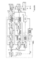
図1は、この発明の実施の形態によるNIMを搭載するCATV向けSTB40のブロック構成図である。STB40では、図8のSTB40Aの構成が簡単化される。
【0042】
STB40はNIMと、STB40Aと同様のトランスポートデコーダ15、MPEG2デコーダ16、マルチプレクサ17、CPU19、QPSK復調器20およびパワーアンプ21とを含む。
【0043】
NIMは入力端子1、HPF3、LPF4、方向性結合器5、アナログデジタル共用チューナ6A、QPSKチューナ8、デジタルSAWフィルタ9A、NTSC復調器10、QPSK復調器11、ダウンコンバータ12、ADC13、QAM復調器14、RFモジュレータ18、出力端子23、RFリレー回路24、データ端子26、AGC切換回路29、IF増幅器30、SW回路31およびアナログSAWフィルタ33を含む。
【0044】
STB40のNIMとSTB40AのNIM1とを比較して異なる点は、NIMはNIM1のデジタルチューナ6、アナログチューナ7、デジタルSAWフィルタ9、両側隣接トラップ回路32およびIF増幅器34に代替して、アナログデジタル共用チューナ6A、デジタルSAWフィルタ9AおよびAGC切換回路29を設け、NIM1の2分配器22に代替してRFリレー回路24を設けた点にある。STB40のNIMの他の構成はSTB40のNIM1のそれと同じであり説明を省略する。
【0045】
図示されるようにNIMではNIM1におけるアナログチューナ7、2分配器22、両側隣接トラップ回路32およびIF増幅器34の削減によりシステムの簡素化が図られて経済的である。
【0046】
このシステムの簡素化のために、アナログデジタル共用チューナ6AとAGC切換回路29とにより図8のアナログチューナ7の機能とデジタルチューナ6の機能とを兼ね備えることができる。
【0047】
また、デジタルSAWフィルタ9Aは図8のデジタルSAWフィルタ9と両側隣接トラップ回路32との機能を兼ね備える。
【0048】
次に、図1に示されたSTB40における動作について説明する。CPU19の出力するデータ信号はQPSK変調器20でQPSK変調されてパワーアンプ21で増幅されて上り信号としてデータ端子26、LPF4、入力端子1および図示されないケーブル回線を介して、たとえば5〜42MHzの帯域を有してCATV局へ送信される。
【0049】
CATV局からケーブル回線を介してSTB40へ送信される、たとえば54〜860MHzの帯域を有する下り信号は入力端子1にて受信される。受信された下り信号は5〜46MHzを減衰域とし54MHz以上を通過域とするHPF3を通って方向性結合器5に与えられる。
【0050】
方向性結合器5に与えられた下り信号は、QPSKチューナ8、QPSK復調器11およびCPU19からなるQPSK信号受信回路とRFリレー回路24に与えられる。
【0051】
RFリレー回路24は接点S1とS2を有して、この2つの接点はCPU19の制御により相互に連動して切換えられる。
【0052】
具体的には、CPU19はNIMを含むSTB40の動作時には、接点S1によって方向性結合器5からの下り信号をアナログデジタル共用チューナ6Aへ出力するとともに接点S2によってRFモジュレータ18からのTV信号を出力端子23へ出力するように、接点S1とS2を切換制御する。逆に動作待機時は、信号がNIMをスルー動作するように、接点S1とS2は連通するように切換制御されて、方向性結合器5から出力される下り信号は直接に出力端子23から外部へ出力される。
【0053】
方向性結合器5で分割された下り信号は、QPSKチューナ8に入力されて選局され、QPSK復調器11によってデータ信号に復調された後、CPU19に与えられて処理される。これに対して、課金情報などの上りデータ信号はCPU19からQPSK変調器20に入力されて変調され、パワーアンプ21で増幅された後、データ端子26に導入され、アップストリーム回路であるLPF4を介して入力端子1からCATVケーブルへ送出される。
【0054】
CPU19はあらかじめプログラムされた手続に従い動作するICであり以下の動作をする。つまり、上述したようにNIMを含むSTB40が受信状態にあるのか待機状態にあるのかを判定して、RFリレー回路24の接点S1とS2を連動して切換制御するとともに、所望の受信チャンネルに応じてアナログデジタル共用チューナ6Aの同調周波数の制御やマルチプレクサ17の切換制御をし、さらにQPSKチューナ8およびQPSK復調器11を用いる下りデータ受信処理およびQPSK変調器20およびパワーアンプ21を用いる上りデータ送信処理を行なう。
【0055】
RFリレー回路24を介してアナログデジタル共用チューナ6Aにて受信された下り信号は、前述したようにアナログ信号であるNTSC映像信号およびデジタル信号であるQAM映像信号を含み、これらの信号はアナログデジタル共用チューナ6AにおいてCPU19の制御に従う同調周波数に基づいて選局処理されて、所望チャンネルのIF信号として出力される。
【0056】
このように、図1の構成ではアナログ放送およびデジタル放送の受信に共用されるアナログデジタル共用チューナ6Aを設けているので、図8の2分配器22によるアナログチューナ7とデジタルチューナ6への信号分配時に入力端子1からデジタルチューナ6までに生じていたロスが低減される。この結果、図1では、受信チャンネルがアナログチャンネルの場合には映像信号に関するSN比が3〜5dB改善され、デジタルチャンネルの場合にはSNRの改善となり、低入力レベル時のBERTの改善となる。
【0057】
また、アナログデジタル共用チューナ6Aを設けて一方のチューナ(図8のアナログチューナ7)および2分配器22が削除されたので、NIMに関してはNIM1に比べて消費電力が約20%削減される。
【0058】
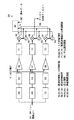
図2は、図1のアナログデジタル共用チューナ6Aのブロック図である。
アナログデジタル共用チューナ6Aはアナログ放送受信用のアナログチャンネルとデジタル方送受信用のデジタルチャンネルの両方についての選局機能を有する。
【0059】
アナログデジタル共用チューナ6Aは前述したB3〜B1バンドのそれぞれについて受信回路を含む。受信回路のそれぞれは入力切換回路68〜70のそれぞれと、高周波増幅入力同調回路53〜55のそれぞれと、高周波増幅部56〜58のぞれぞれと、高周波増幅出力同調回路71〜73のそれぞれと、混合回路59〜61のそれぞれと、局部発振回路62〜64のそれぞれとを含むとともにB3〜B1バンドについて共用されるPLL選局回路95を含む。
【0060】
局部発振回路62〜64のそれぞれは、PLL選局回路95から与えられる同調電圧TVに応じた周波数で発振するとともに発振出力fvをPLL選局回路95と対応の混合回路に与える。
【0061】
上述した各バンドの受信回路ごとに設けられた混合回路と局部発振回路と各バンドに共通して設けられたPLL選局回路95とにより各バンドごとの周波数変換回路が形成される。
【0062】
各バンドの周波数変換回路は同様の動作をする。つまり、局部発振回路はPLL選局回路95により印加される所望チャンネルに対応の同調電圧TVのレベルに従う同調周波数で発振動作するので、混合回路では前段の高周波増幅出力同調回路から入力されるRF信号は対応の局部発振回路から出力される発振出力fvと混合されて、所望チャンネルに対応のIF信号に変換されて出力される。
【0063】
アナログデジタル共用チューナ6Aの動作において、RFリレー回路24から出力されたCATV局からの下り信号は各バンドの受信回路に与えられる。
【0064】
各バンドの受信回路は所望される受信チャンネルに応じて択一的に選択されて、選択された受信回路のみが動作状態となり、選択されないものは非動作状態となる。
【0065】
具体的にはCPU19によりPLL選局回路95に選局データSDとして与えられる所望される受信チャンネル情報とバンド情報とに応じて入力切換回路68〜70のいずれか1つが選択的に動作して、動作した入力切換回路により対応するバンドの受信回路への電源供給切換が行なわれて、機能の動作制御が行なわれる。
【0066】
たとえば、B3バンドのチャンネル受信時には入力切換回路68、高周波増幅入力同調回路53、高周波増幅部56、高周波増幅出力同調回路71、混合回路59、局部発振回路62およびPLL選局回路95は動作状態であり、B2およびB1バンドの受信回路、すなわち入力切換回路69と70、高周波増幅入力同調回路54と55、高周波増幅部57と58、高周波増幅出力同調回路72と73、混合回路60と61および局部発振回路63と64は非動作状態となる。
【0067】
なお、PLL選局回路95は各バンドに共通な回路なので、常時動作状態となる。
【0068】
同様にして、B2バンドのチャンネル受信時にはB2バンドの受信回路のみ動作状態となり、B1およびB3の受信回路は非動作状態となる。同様にB3バンドのチャンネル受信時にはB3バンドの受信回路のみ動作状態となり、B1およびB2の受信回路は非動作状態となる。
【0069】
次に、各バンドの受信回路での動作を説明する。
各バンドの受信回路での動作は同じなので、ここではB3バンドの受信回路を例にして説明し、B2およびB1バンドの受信回路の動作は説明を省略する。
【0070】
入力切換回路68を介してRFリレー回路24から入力された下り信号(RF信号)は、高周波増幅入力同調回路53にて所望受信チャンネルに対応の周波数の信号が取り出されて、高周波増幅部56に与えられる。高周波増幅部56では、AGC切換回路29から印加されるAGC電圧Vに従って入力信号を増幅して高周波増幅出力同調回路71に出力する。
【0071】
図1のAGC切換回路29はアナログデジタル共用チューナ6Aに関連して設けられる。アナログデジタル共用チューナ6Aの高周波増幅部56〜58に印加される自動利得制御のためのAGC電圧Vは、アナログ放送受信時とデジタル放送受信時とで、利得が減衰し始める値および傾きが異なっているので、AGC切換回路29はアナログ放送受信時とデジタル放送受信時とでAGC電圧Vのレベルを切換えることによってアナログ放送受信およびデジタル放送受信のためのチューナの共用化を可能としている。
【0072】
このAGC切換回路29の切換え動作は以下のように行なわれる。つまり、AGC切換回路29はデジタル放送受信時はQAM復調回路14からの復調結果S1に基づいて、アナログ放送受信時はNTSC復調回路10からの復調結果S2に基づいてAGC電圧Vのレベルを切換える。
【0073】
高周波増幅出力同調回路71は、与えられる信号を入力して再度、所望受信チャンネルに対応する周波数の信号を取出して混合回路59、局部発振回路62およびPLL選局回路95からなる周波数変換回路に与える。
【0074】
周波数変換回路では、前述したように与えられた所望チャンネルに対応のRF信号がIF信号に変換される。
【0075】
ここで、デジタル放送受信のためのチャンネルおよびアナログ放送受信のためのチャンネルのチューニングに共用されるPLL選局回路95について説明する。
【0076】
デジタル放送受信専用のチューナに適用されるPLL選局方式およびアナログ放送受信専用のチューナに適用されるPLL選局方式の相違点は、PLLにおける比較周波数およびチューニングステップにおいて相違する。具体的には、アナログ系では変調信号は残留側波帯(VSB)方式を採用しているためにIF周波数精度を高くする必要があるので、比較周波数において10KHz以下の低い周波数が用いられるのに対し、デジタル系ではVCO(Voltage Control Oscillatorの略)におけるフェーズノイズを低減させるために、比較周波数において62.5KHz、125KHzおよび250KHzなどの比較的高い周波数が用いられる。
【0077】
そこで、本実施の形態では、アナログデジタル共用チューナ6Aにおいて1個のPLL ICにてデジタルチューナおよびアナログチューナの両機能を満たすようにするため、基準周波数を分周する機能を有して、特に所望受信チャンネルがアナログチャンネルである場合およびデジタルチャンネルである場合に応じて基準周波数の分周比を可変設定するよう構成される。
【0078】
具体的には、PLLシステムにおける基準発振信号を分周し位相検波器に印加される従来方式を、分周回路をプログラム設定が可能なシステムに変更する。たとえば、デジタルチャンネル受信の場合、4MHzの基準信号周波数を32分周することにより125KHzの比較周波数に、アナログチャンネルの受信の場合、256分周または512分周により15.625KHzまたは7.8125KHzの比較周波数になるよう分周比を各チャンネルごとにプログラム設定するシステムとすることにより、チューナのアナログ放送およびデジタル放送での共用化が可能となる。
【0079】
図3は、図2のPLL選局回路のブロック構成図である。PLL選局回路95は1チップICからなり、前置分周器951、プログラマブル可変分周器952と954、周波数位相比較器953、LPF(ループフィルタ)955および水晶発振器等からなる基準発振器956を含む。
【0080】
プログラマブル可変分周器954には、前述したようにCPU19からの選局データSDに基づいて受信チャンネルがアナログチャンネルであるかデジタルチャンネルであるかに応じた分周比Mが予めプログラム設定される。同様に、プログラマブル分周器952には、CPU19からの選局データSDに基づいて所望受信チャンネルに応じた分周比Nが予めプログラム設定される。
【0081】
動作において、基準発振器956の発振出力はプログラマブル可変分周器954においてCPU19からの選局データSDに基づく分周比Mで分周されて比較周波数信号として周波数位相比較器953に与えられる。また、局部発振回路(62,63、64)の発振出力fvは、RF信号であるのでまず前置分周器951により後段の回路で処理しやすい周波数にまで分周されてプログラマブル分周器952に与えられる。プログラマブル分周器952では発振出力fvは選局データSDに基づく分周比Nで分周された後、周波数位相比較器953に与えられて、ここで可変分周器954からの比較周波数信号と比較されて、比較結果に基づきLPF(ループフィルタ)955を介して両信号の位相差が一定となるような同調電圧TVが局部発振回路(62,63、64)に印加される。
【0082】
このようにして、アナログデジタル共用チューナ6Aから出力された所望受信チャンネルに対応するIF信号はデジタルSAWフィルタ9Aに与えられる。
【0083】
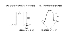
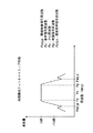
図4(A)と(B)は、図1のデジタルSAWフィルタ9Aの両側隣接チャンネル妨害の除去比について説明する図である。ここで、デジタルSAWフィルタ9Aについて説明する。
【0084】
従来、デジタル放送用のSAWフィルタは通信速度に応じて伝送帯域幅が決定されているので、復調系ではアナログ放送およびデジタル放送についてそれぞれ専用にSAWフィルタが設けられるのが通例である。また、一方では、近年世界各国のデジタル放送の信号波に関する規格(DVB−C、MCMSなど)が決定されており通信速度が定まりつつある。このような背景から、デジタル放送用のSAWフィルタの伝送帯域幅は、たとえばアメリカ合衆国向けの仕様であれば6MHzに、ヨーロッパ向けの仕様であれば8MHzにセットされる。
【0085】
これに対して従来のアナログ放送用のSAWフィルタの伝送帯域幅は、アメリカ合衆国向け仕様でNTSCの帯域幅、ヨーロッパの仕様でPALの帯域幅に相当する。通過帯域幅はNTSCで4.5MHz、PALで5.5MHzがそれぞれ必要とされる。このことから、SAWフィルタに必要とされるアナログ放送向けの通過帯域幅は、デジタル放送向けの通過帯域幅に含まれるので、アナログチャンネル受信時、アナログ放送のIF信号をデジタル放送向けのSAWフィルタ9Aを用いて処理することが可能となる。これにより、SAWフィルタ9Aを用いて処理する方法によれば所望受信チャンネルにおける信号が両側隣接チャンネルの信号により変調されて混信状態が生じる現象(以下、両側隣接チャンネル妨害という)において変調を引き起こす妨害波の除去比が以下のように改善される。
【0086】
つまり、アナログのIF信号に関して図4(B)の従来の両側隣接トラップ回路32を用いた場合の妨害波の除去比H2と、図4(A)の図1のデジタルSAWフィルタ9Aを用いた場合の妨害波の除去比H1とを比較すると、H1>H2となり除去比H1は除去比H2に対して10dB以上改善される。また、NIMに関して両側隣接チャンネル妨害を除去するためのトラップ調整が必要ない構成となるので経済的である。
【0087】
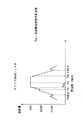
図5は、アナログIF信号における両側隣接トラップ特性を示す図である。図示されるようにアナログIF信号の両側隣接チャンネル妨害の除去比は10数dBである。
【0088】
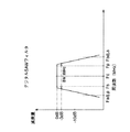
図6は、アナログSAWフィルタ33の特性を示す図である。ここに示されるようにアナログSAWフィルタ33では両側隣接チャンネル妨害の除去比は40dB以上である。それゆえに、図5に示されるアナログIF信号に関する両側隣接チャンネルのトラップ特性を満足させるためには、図8に示されるアナログSAWフィルタ33の他に、両側隣接チャンネル妨害を十分に減衰させるための両側隣接トラップ回路32が必要とされるが、この場合でも計算上除去比として60dB以上確保することは困難である。
【0089】
図7は、デジタルSAWフィルタ9Aの特性を示す図である。図示されるようにアナログIF信号に関してデジタルSAWフィルタ9Aを従来の両側隣接トラップ回路32の代わりに用いることにより、両側隣接チャンネル妨害の除去比を60dB以上確保することが可能となる。
【0090】
また、デジタルSAWフィルタ9Aを用いた構成では、バンドエッジ(受信チャンネルの帯域の両エッジ)において群遅延時間が良好である。すなわち、従来の図8の構成では、信号は両側隣接トラップ回路32を通過するのでその分の群遅延時間が生じていたが、図1のデジタルSAWフィルタ9Aを用いた構成では両側隣接トラップ回路32が削除されるのでその分の群遅延時間が除かれる。
【0091】
このように、本来の帯域制限特性の他に両側隣接チャンネル妨害に関するトラップ特性を有したデジタルSAWフィルタ9Aから出力されたIF信号はIF増幅器30にて増幅された後、SW回路31に与えられる。
【0092】
SW回路31はQAM復調器14の出力する切換信号CHにより切換制御されて動作する電子スイッチ回路である。すなわちQAM復調器14が直列ビットストリームを出力しているデジタル放送受信時は、SW回路31は切換信号CHに従い、与えられるデジタルのIF信号を入力してデジタル復調系側のダウンコンバータ12に出力する。逆に、QAM復調器14が直列ビットストリームを出力していないアナログ放送受信時は、SW回路31は切換信号CHに従って、与えられるアナログのIF信号を入力してアナログ復調系側のアナログSAWフィルタ33に与える。
【0093】
このように、アナログチャンネルの信号およびデジタルチャンネルの信号は電子SW回路31によりアナログ復調系側の回路群およびデジタル復調系側の回路群でそれぞれ個別に処理されるように分岐されるから、互いの干渉は防止されて良好な受信状態が得られる。
【0094】
アナログのIF信号がアナログSAWフィルタ33を介してNTSC復調器10にて復調されてコンポジット信号CP1としてマルチプレクサ17に与えられる。
【0095】
デジタルのIF信号はダウンコンバータ12にて低周波のIF信号に変換されて、ADC13に与えられる。
【0096】
ADC13ではデジタルのIF信号は、8ビットまたは10ビットのデジタル信号に変換されてQAM復調器14に与えられる。
【0097】
QAM復調器14は与えられるデジタル信号をI、Q復調して、誤り訂正した後、直列のビットストリームとしてトランスポートデコーダ15に出力する。
【0098】
トランスポートデコーダ15は、与えられる直列ビットストリームから映像および音声信号を取出してMPEG2デコーダ16に出力する。
【0099】
MPEG2デコーダ16は、入力する映像および音声信号の帯域伸長を行ない、アナログのNTSCのコンポジット信号CP2としてマルチプレクサ17に出力する。
【0100】
マルチプレクサ17はCPU19の制御に従い、コンポジット信号CP1およびCP2のうち所望される受信チャンネルに該当するいずれか一方のコンポジット信号をRFモジュレータ18に出力する。
【0101】
つまり、CPU19は所望受信チャンネルがデジタルチャンネルである場合にはコンポジット信号CP2が、逆にアナログチャンネルである場合にはコンポジット信号CP1が選択されてRFモジュレータ18に出力されるようにマルチプレクサ17を切換制御する。
【0102】
RFモジュレータ18は、与えられるコンポジット信号を所望されるチャンネルのTV信号に変換して出力する。このTV信号はRFリレー回路24の接点S2を介して出力端子23から図示されないTV受像機のアンテナ入力端子に出力される。
【0103】
今回開示された実施の形態はすべての点で例示であって制限的なものではないと考えられるべきである。本発明の範囲は上記した説明ではなくて特許請求の範囲によって示され、特許請求の範囲と均等の意味および範囲内でのすべての変更が含まれることが意図される。
【図面の簡単な説明】
【図1】この発明の実施の形態によるNIMを搭載するCATV向けSTBのブロック構成図である。
【図2】図1のアナログデジタル共用チューナ6Aのブロック図である。
【図3】図2のPLL選局回路のブロック構成図である。
【図4】(A)と(B)は、図1のデジタルSAWフィルタ9Aの両側隣接チャンネル妨害の除去比について説明する図である。
【図5】アナログIF信号における両側隣接トラップ特性を示す図である。
【図6】アナログSAWフィルタの特性を示す図である。
【図7】デジタルSAWフィルタの特性を示す図である。
【図8】従来のSTBのブロック構成図である。
【符号の説明】
6A アナログデジタル共用チューナ
9A デジタルSAWフィルタ
10 NTSC復調器
14 QAM復調器
19 CPU
24 RFリレー回路
29 AGC切換回路
30 IF増幅器
31 SW回路
40 STB[0001]
BACKGROUND OF THE INVENTION
The present invention relates to a NIM (abbreviation of network interface module) suitably used for a cable modem or STB (abbreviation of set top box) for CATV (abbreviation of cable television), and more particularly to an NIM whose circuit configuration is improved. .
[0002]
[Prior art]
CATV operators are using HFC (Hybrid Fiber Coax), which uses coaxial cables for home service lines and optical fiber for the trunk network to provide multi-channel and broadband data communication services using empty channels. ). Thus, for example, by using 64-value QAM (Quadrature Phase Modulation), a high-speed data line having a transmission rate of 30 Mbit / s can be created with a bandwidth of 6 MHz for one channel. In such a cable modem or STB for CATV, a NIM is mounted for communication connection between the cable network and the home side.
[0003]
FIG. 8 is a block diagram of a
In FIG. 8, the STB 40A includes an
[0004]
A signal transmitted from the
[0005]
The STB 40A is a NIM1, a
phase shift keying) including a
[0006]
The NIM 1 includes an
television system committee)
[0007]
The upstream signal is amplified by the
[0008]
Each of the tuners 6 to 8 is a UHF band (B3 band) that receives 470 to 860 MHz, a VHF High band (B2 band) that receives 170 MHz to 470 MHz, and a VHF Low band (B1 band) that receives 54 to 170 MHz. It consists of a receiving circuit for each band. However, the band division is not specified in this.
[0009]
The downstream signal passes through the
[0010]
The types of CATV signals in recent years are divided into QPSK-modulated upstream and downstream signals, analog NTSC video signals, and digital QAM video signals. In the
[0011]
Analog NTSC video signals are processed by analog video signal receiving circuits (circuits 7 to 10), and digital QAM video signals are processed by QAM signal receiving circuits (
[0012]
First, the NTSC video signal, which is a downstream analog signal, passes through the
[0013]
On the other hand, the QAM-modulated digital signal passes through the
[0014]
This digital signal is subjected to I and Q demodulation and error correction by the
[0015]
The
[0016]
The
[0017]
Next, for communication between the center side which is a CATV station and the
[0018]
An upstream data signal such as billing information is supplied from the
[0019]
[Problems to be solved by the invention]
Since the STB or cable modem for CATV is required to be downsized, the NIM mounted thereon is also required to be downsized as an RF module.
[0020]
However, if the conventional NIM shown in FIG. 8 is modularized as it is, it becomes large in size, and downsizing of the STB or cable modem on which the NIM is mounted is hindered.
[0021]
SUMMARY OF THE INVENTION Therefore, an object of the present invention is to provide a network interface module that is simplified in configuration and reduced in size.
[0022]
[Means for Solving the Problems]
The network interface module according to
[0023]
That means Via the terminal for signal transmission / reception A low-pass filter for sending the upstream data signal to the CATV station on the cable line; Has a different passband from the low-pass filter Analog broadcast signal from CATV station , Signals for digital broadcasting And downstream data signal Downstream signal including Via the aforementioned terminal At least a high-pass filter for introducing from a cable line and a receiving circuit for receiving a downlink signal introduced by the high-pass filter are provided.
[0024]
The receiving circuit has the following characteristics. That means A data demodulation circuit that inputs and demodulates a downstream signal and outputs a downstream data signal; A downstream signal is input and amplified with a predetermined gain, and then converted to an intermediate frequency signal of a desired channel for analog broadcasting or digital broadcasting and output. One Tuner, A branching unit that inputs the downstream signal introduced by the high-pass filter, branches to the data demodulating circuit and the tuner, and outputs; The intermediate frequency signal of the desired channel output from the tuner is input, the SAW filter that removes the interference wave due to the adjacent channel in the desired channel while outputting the band is limited, and the intermediate frequency signal of the desired channel output from the SAW filter Amplification unit that inputs and amplifies and outputs, and intermediate frequency signal of desired channel output from amplification unit is input and demodulated Then output Demodulator And a signal switching unit that inputs an analog broadcast signal or a digital broadcast signal output from the demodulation unit, and switches to one of the input signals based on whether the desired channel is for analog broadcast or digital broadcast. In addition, a downstream signal provided between the branching unit and the tuner and output from the branching unit is input and selectively output to either the tuner or the outside, and the signal output from the signal switching unit is input High frequency relay circuit to selectively switch to output or not output to the outside With.
[0025]
According to the first aspect of the present invention, there is one tuner that processes a downstream signal including an analog broadcast signal and a digital broadcast signal, and the SAW filter has a function of removing interference waves caused by adjacent channels in a desired channel. .
[0026]
Therefore, compared to a conventional analog broadcast signal and a digital broadcast signal individually provided with a tuner, and further provided with a circuit for individually removing the interference wave due to the adjacent channel to perform signal processing, The number of circuit points is reduced and the configuration is simplified. Also, the delay time related to the signal is improved, and the reception quality is improved.
[0027]
Further, the downstream signal can be processed by one tuner, and the power consumption is reduced as compared with the case where the downstream signal is processed by two conventional tuners.
[0028]
In addition, a path including a circuit for distributing the downlink signal received to the two tuners is not necessary as compared with the conventional one, and the signal distribution loss is improved correspondingly, and the reception quality is improved.
[0029]
According to a second aspect of the present invention, there is provided the network interface module according to the first aspect, wherein the tuner of the network interface module according to the first aspect converts an incoming downlink signal into an intermediate frequency signal of a desired channel based on a level of a selected channel selection signal. A conversion circuit and a channel selection circuit that outputs a channel selection signal to the conversion circuit, and the channel selection circuit determines the level of the channel selection signal based on information of a desired channel.
[0030]
According to the second aspect, an intermediate frequency signal corresponding to each of the desired channels for analog broadcasting and digital broadcasting can be obtained based on the information of the desired channel.
[0031]
Therefore, since the tuning circuit and the conversion circuit are shared for analog broadcasting and digital broadcasting in the tuner, the configuration of the tuner itself is simplified.
[0032]
In the network interface module according to claim 3, the predetermined gain in the tuner of the network interface module according to
[0033]
According to the third aspect, the downstream signal is amplified by the tuner with a gain according to the demodulation result.
[0034]
Therefore, a circuit unit for amplifying a downstream signal having a high frequency in the tuner is also shared for analog broadcasting and digital broadcasting, and the configuration of the tuner itself is simplified.
[0035]
In the network interface module according to a fourth aspect, the demodulator of the network interface module according to any one of the first to third aspects is configured as follows. That is, the demodulator inputs the intermediate frequency signal of the desired channel output from the amplifying unit, and in one direction when the desired channel is an analog broadcast channel, and in the other direction when the desired channel is a digital broadcast channel. The analog demodulation circuit for inputting and demodulating the intermediate frequency signal of the desired channel output from the switching circuit in one direction, and the desired channel output from the switching circuit in the other direction. And a digital demodulator circuit that receives and demodulates the intermediate frequency signal.
[0036]
According to the fourth aspect of the present invention, in the demodulator, the intermediate frequency signal of the desired channel is either an analog demodulator circuit or a digital demodulator circuit which is separated from each other depending on whether the signal is for analog broadcast or digital broadcast. Is selectively demodulated.
[0037]
Accordingly, mutual interference is avoided between signals between both demodulation circuits, and the reception quality is improved.
[0040]
[0041]
DETAILED DESCRIPTION OF THE INVENTION
FIG. 1 is a block diagram of a
[0042]
The
[0043]
NIM is
[0044]
The difference between the NIM of STB40 and NIM1 of STB40A is that NIM replaces NIM1's digital tuner 6, analog tuner 7,
[0045]
As shown in the figure, the NIM is economical because the system is simplified by reducing the analog tuner 7, the two
[0046]
In order to simplify this system, the analog / digital shared
[0047]
The digital SAW filter 9A also has the functions of the
[0048]
Next, the operation of the
[0049]
A downlink signal having a bandwidth of 54 to 860 MHz, for example, transmitted from the CATV station to the
[0050]
The downstream signal supplied to the
[0051]
The
[0052]
Specifically, the
[0053]
The downlink signal divided by the
[0054]
[0055]
The downstream signal received by the analog / digital shared
[0056]
As described above, in the configuration of FIG. 1, the analog / digital shared
[0057]
Also, A Since one tuner (analog tuner 7 in FIG. 8) and the two
[0058]
FIG. 2 is a block diagram of the analog / digital shared
The analog / digital shared
[0059]
The analog / digital shared
[0060]
Each of the local oscillation circuits 62 to 64 oscillates at a frequency corresponding to the tuning voltage TV supplied from the PLL
[0061]
A frequency conversion circuit for each band is formed by the above-described mixing circuit, local oscillation circuit, and PLL
[0062]
The frequency conversion circuit of each band performs the same operation. That is, since the local oscillation circuit oscillates at a tuning frequency according to the level of the tuning voltage TV corresponding to the desired channel applied by the PLL
[0063]
In the operation of the analog / digital shared
[0064]
The reception circuit of each band is alternatively selected according to a desired reception channel, and only the selected reception circuit is in an operating state, and those not selected are in an inoperative state.
[0065]
Specifically, any one of the
[0066]
For example, when receiving the B3 band channel, the
[0067]
Since the PLL
[0068]
Similarly, when the B2 band channel is received, only the B2 band receiving circuit is activated, and the B1 and B3 receiving circuits are deactivated. Similarly, at the time of B3 band channel reception, only the B3 band receiving circuit is activated, and the B1 and B2 receiving circuits are deactivated.
[0069]
Next, the operation of the receiving circuit for each band will be described.
Since the operation of the reception circuit in each band is the same, the description will be given by taking the reception circuit of the B3 band as an example, and the description of the operation of the reception circuit of the B2 and B1 bands will be omitted.
[0070]
As for the downstream signal (RF signal) input from the
[0071]
The
[0072]
The switching operation of the
[0073]
The high frequency amplification
[0074]
In the frequency conversion circuit, the RF signal corresponding to the given desired channel is converted into an IF signal as described above.
[0075]
Here, the PLL
[0076]
The difference between the PLL channel selection method applied to the tuner dedicated to digital broadcast reception and the PLL channel selection method applied to the tuner dedicated to analog broadcast reception differ in the comparison frequency and the tuning step in the PLL. Specifically, in the analog system, since the modulation signal uses the residual sideband (VSB) method, it is necessary to increase the IF frequency accuracy, so a low frequency of 10 KHz or less is used as the comparison frequency. On the other hand, in the digital system, relatively high frequencies such as 62.5 KHz, 125 KHz, and 250 KHz are used in the comparison frequency in order to reduce phase noise in a VCO (abbreviation of Voltage Control Oscillator).
[0077]
Therefore, in this embodiment, in order to satisfy both the functions of the digital tuner and the analog tuner with one PLL IC in the analog / digital shared
[0078]
Specifically, the conventional method in which the reference oscillation signal in the PLL system is divided and applied to the phase detector is changed to a system in which the frequency dividing circuit can be programmed. For example, in the case of digital channel reception, a reference signal frequency of 4 MHz is divided by 32 to a comparison frequency of 125 KHz, and in the case of reception of an analog channel, comparison is made by 15.625 KHz or 7.8125 KHz by division by 256 or 512. By adopting a system in which the frequency division ratio is set for each channel so as to obtain a frequency, the tuner can be shared by analog broadcasting and digital broadcasting.
[0079]
FIG. 3 is a block diagram of the PLL channel selection circuit of FIG. The PLL
[0080]
The programmable
[0081]
In operation, the oscillation output of the
[0082]
In this way, the IF signal corresponding to the desired reception channel output from the analog / digital shared
[0083]
4A and 4B are diagrams for explaining the rejection ratio of the adjacent channel interference on both sides of the digital SAW filter 9A of FIG. Here, the digital SAW filter 9A will be described.
[0084]
Conventionally, since the transmission bandwidth of a SAW filter for digital broadcasting is determined according to the communication speed, a SAW filter is usually provided exclusively for analog broadcasting and digital broadcasting in the demodulation system. On the other hand, in recent years, standards (DVB-C, MCMS, etc.) relating to digital broadcast signal waves in various countries around the world have been determined, and the communication speed is being determined. From such a background, the transmission bandwidth of the SAW filter for digital broadcasting is set to 6 MHz for the specification for the United States, for example, and 8 MHz for the specification for Europe.
[0085]
On the other hand, the transmission bandwidth of a conventional analog broadcast SAW filter corresponds to the NTSC bandwidth in the US specification and the PAL bandwidth in the European specification. The passband width is 4.5 MHz for NTSC and 5.5 MHz for PAL. Therefore, the pass bandwidth for analog broadcasting required for the SAW filter is included in the pass bandwidth for digital broadcast. Therefore, when receiving an analog channel, the analog broadcast IF signal is converted into a digital broadcast SAW filter 9A. It becomes possible to process using. Thus, according to the method of processing using the SAW filter 9A, the interference wave that causes the modulation in the phenomenon that the signal in the desired reception channel is modulated by the signal of the adjacent channel on both sides and the interference state occurs (hereinafter referred to as the adjacent channel interference on both sides). The removal ratio is improved as follows.
[0086]
That is, for the analog IF signal, the interference wave rejection ratio H2 in the case where the conventional both-side
[0087]
FIG. 5 is a diagram illustrating both-side adjacent trap characteristics in an analog IF signal. As shown in the figure, the rejection ratio of the adjacent channel interference on the analog IF signal is 10 and several dB.
[0088]
FIG. 6 is a diagram illustrating the characteristics of the
[0089]
FIG. 7 is a diagram showing the characteristics of the digital SAW filter 9A. As shown in the figure, by using the digital SAW filter 9A in place of the conventional both-side
[0090]
In the configuration using the digital SAW filter 9A, the group delay time is good at the band edge (both edges of the band of the reception channel). That is, in the conventional configuration of FIG. 8, since the signal passes through the both-side
[0091]
As described above, the IF signal output from the digital SAW filter 9A having the trap characteristic regarding the adjacent channel interference in addition to the original band limiting characteristic is amplified by the
[0092]
The
[0093]
In this way, the analog channel signal and the digital channel signal are branched by the
[0094]
The analog IF signal is demodulated by the
[0095]
The digital IF signal is converted into a low-frequency IF signal by the
[0096]
In the
[0097]
The
[0098]
The
[0099]
The
[0100]
The
[0101]
That is, the
[0102]
The
[0103]
The embodiment disclosed this time should be considered as illustrative in all points and not restrictive. The scope of the present invention is defined by the terms of the claims, rather than the description above, and is intended to include any modifications within the scope and meaning equivalent to the terms of the claims.
[Brief description of the drawings]
FIG. 1 is a block diagram of a STB for CATV equipped with a NIM according to an embodiment of the present invention.
FIG. 2 is a block diagram of the analog / digital shared
3 is a block configuration diagram of the PLL channel selection circuit of FIG. 2;
4A and 4B are diagrams for explaining a rejection ratio of adjacent channel interference on both sides of the digital SAW filter 9A of FIG.
FIG. 5 is a diagram showing both-side adjacent trap characteristics in an analog IF signal.
FIG. 6 is a diagram illustrating characteristics of an analog SAW filter.
FIG. 7 is a diagram illustrating characteristics of a digital SAW filter.
FIG. 8 is a block diagram of a conventional STB.
[Explanation of symbols]
6A Analog digital tuner
9A Digital SAW filter
10 NTSC demodulator
14 QAM demodulator
19 CPU
24 RF relay circuit
29 AGC switching circuit
30 IF amplifier
31 SW circuit
40 STB
Claims (4)
信号送受信の端子を介して前記ケーブル回線に前記CATV局への上りデータ信号を送出するためのローパスフィルタと、
前記ローパスフィルタとは異なる通過帯域を有し前記CATV局からのアナログ放送用の信号、デジタル放送用の信号および下りデータ信号を含む下り信号を前記端子を介して前記ケーブル回線から導入するためのハイパスフィルタと、
前記ハイパスフィルタにより導入された前記下り信号を受信するための受信回路とを、少なくとも備え、
前記受信回路は、
前記下り信号を入力して復調して前記下りデータ信号を出力するデータ復調回路と、
前記下り信号を入力して所定利得で増幅した後に前記アナログ放送用および前記デジタル放送用のいずれかの所望チャンネルの中間周波信号に変換して出力する1つのチューナと、
前記ハイパスフィルタにより導入された前記下り信号を入力して前記データ復調回路と前記チューナに分岐して出力する分岐部と、
前記チューナから出力される前記所望チャンネルの中間周波信号を入力して、帯域制限しながら前記所望チャンネルにおける近接チャンネルによる妨害波を除去して出力するSAWフィルタと、
前記SAWフィルタから出力された前記所望チャンネルの中間周波信号を入力して増幅して出力する増幅部と、
前記増幅部から出力された前記所望チャンネルの中間周波信号を入力して、復調して出力する復調部と、
前記復調部から出力される前記アナログ放送用または前記デジタル放送用の信号を入力して、前記所望チャンネルの前記アナログ放送用および前記デジタル放送用の別に基づき、いずれか一方の入力信号に切換えて出力する信号切換部と、
前記分岐部と前記チューナとの間に設けられて、前記分岐部により出力された前記下り信号を入力して前記チューナおよび外部のいずれか一方に選択的に出力するとともに、前記信号切換部から出力された信号を入力して、前記外部に出力するか出力しないように選択的に切換える高周波リレー回路とを備える、ネットワークインターフェイスモジュール。A network interface module for transmitting / receiving signals to / from a CATV station via a cable line,
A low-pass filter for sending an upstream data signal to the CATV station via the signal transmission / reception terminal ;
Pass for introducing from the cable line a downlink signal through the terminal including the signals for analog broadcast from the CATV station has a different pass band than the low pass filter, signal and downlink data signals for digital broadcast Filters,
A reception circuit for receiving the downlink signal introduced by the high-pass filter, at least,
The receiving circuit is
A data demodulation circuit that inputs and demodulates the downlink signal and outputs the downlink data signal;
One tuner that inputs the downstream signal and amplifies it with a predetermined gain, and then converts it into an intermediate frequency signal of any desired channel for analog broadcasting and digital broadcasting, and outputs it.
A branching unit that inputs the downstream signal introduced by the high-pass filter and branches and outputs the data demodulating circuit and the tuner;
An SAW filter that inputs an intermediate frequency signal of the desired channel output from the tuner, removes an interference wave due to a neighboring channel in the desired channel while limiting the band, and outputs the interference wave;
An amplifying unit that inputs, amplifies and outputs the intermediate frequency signal of the desired channel output from the SAW filter;
A demodulator that inputs and demodulates and outputs the intermediate frequency signal of the desired channel output from the amplifier ;
The analog broadcast or digital broadcast signal output from the demodulator is input, and the desired channel is switched to one of the input signals based on the analog broadcast and the digital broadcast. A signal switching unit to perform,
Provided between the branching unit and the tuner, the downstream signal output from the branching unit is input, selectively output to either the tuner or the outside, and output from the signal switching unit And a high frequency relay circuit that selectively switches the signal to be output to the outside or not to be output to the outside .
入力する前記下り信号を、与えられる選局信号のレベルに基づいて前記所望チャンネルの中間周波信号に変換するための変換回路と、
前記変換回路に前記選局信号を出力する選局回路とを含み、
前記選局回路は、前記所望チャンネルの情報に基づいて前記選局信号のレベルを決定することを特徴とする、請求項1に記載のネットワークインターフェイスモジュール。The tuner is
A conversion circuit for converting the downstream signal to be input into an intermediate frequency signal of the desired channel based on a level of a selected channel selection signal;
A tuning circuit that outputs the tuning signal to the conversion circuit,
The network interface module according to claim 1, wherein the channel selection circuit determines a level of the channel selection signal based on information of the desired channel.
前記増幅部から出力された前記所望チャンネルの中間周波信号を入力して、前記所望チャンネルが前記アナログ放送用のチャンネルである場合に一方向に、前記デジタル放送用のチャンネルである場合に他方向にそれぞれ出力する切換回路と、
前記一方向において、前記切換回路から出力される前記所望チャンネルの中間周波信号を入力して復調するアナログ復調回路と、前記他方向において、前記切換回路から出力される前記所望チャンネルの中間周波信号を入力して復調するデジタル復調回路とを分離して備える、請求項1ないし3のいずれかに記載のネットワークインターフェイスモジュール。The demodulator
The intermediate frequency signal of the desired channel output from the amplifying unit is input, and when the desired channel is the analog broadcast channel, it is unidirectional, and when the desired channel is the digital broadcast channel, the other direction. A switching circuit for outputting each;
An analog demodulation circuit that receives and demodulates an intermediate frequency signal of the desired channel output from the switching circuit in the one direction, and an intermediate frequency signal of the desired channel output from the switching circuit in the other direction. 4. The network interface module according to claim 1, further comprising a digital demodulator circuit that receives and demodulates the network interface module.
Priority Applications (1)
| Application Number | Priority Date | Filing Date | Title |
|---|---|---|---|
| JP34140598A JP3668024B2 (en) | 1998-12-01 | 1998-12-01 | Network interface module |
Applications Claiming Priority (1)
| Application Number | Priority Date | Filing Date | Title |
|---|---|---|---|
| JP34140598A JP3668024B2 (en) | 1998-12-01 | 1998-12-01 | Network interface module |
Publications (2)
| Publication Number | Publication Date |
|---|---|
| JP2000175164A JP2000175164A (en) | 2000-06-23 |
| JP3668024B2 true JP3668024B2 (en) | 2005-07-06 |
Family
ID=18345820
Family Applications (1)
| Application Number | Title | Priority Date | Filing Date |
|---|---|---|---|
| JP34140598A Expired - Fee Related JP3668024B2 (en) | 1998-12-01 | 1998-12-01 | Network interface module |
Country Status (1)
| Country | Link |
|---|---|
| JP (1) | JP3668024B2 (en) |
Families Citing this family (2)
| Publication number | Priority date | Publication date | Assignee | Title |
|---|---|---|---|---|
| JP2007096536A (en) * | 2005-09-27 | 2007-04-12 | Maspro Denkoh Corp | Cable modem |
| JP4882989B2 (en) | 2007-12-10 | 2012-02-22 | ソニー株式会社 | Electronic device, reproduction method and program |
-
1998
- 1998-12-01 JP JP34140598A patent/JP3668024B2/en not_active Expired - Fee Related
Also Published As
| Publication number | Publication date |
|---|---|
| JP2000175164A (en) | 2000-06-23 |
Similar Documents
| Publication | Publication Date | Title |
|---|---|---|
| JPH11341453A (en) | Network interface module | |
| US6088569A (en) | Method and apparatus for receiving a plurality of signals having different frequency bandwidths | |
| JP2008312136A (en) | Cable communication apparatus and cable communication method | |
| JP4467383B2 (en) | Digital broadcasting tuner | |
| US7421040B2 (en) | Modem tuner | |
| JP3668024B2 (en) | Network interface module | |
| JP2004519871A (en) | Television receiver for digital signals with offset tuning means | |
| JP3850225B2 (en) | Tuner for cable modem | |
| US20090180035A1 (en) | Filter arrangement for a tuner in a broadband receiver | |
| KR100703078B1 (en) | Bidirection receiver for cable broadcating | |
| JP3598773B2 (en) | Digital CATV system and its receiving device | |
| JP3296721B2 (en) | Set top converter | |
| JP2000059746A (en) | CATV system and its terminal device | |
| JP4029894B2 (en) | Sending method | |
| JP3783704B2 (en) | Receiver | |
| JP3986773B2 (en) | Terrestrial digital broadcast reception tuner | |
| JPH11103427A (en) | Tuner for cable modem | |
| JP3308648B2 (en) | Broadband DBS tuner | |
| JP3583760B2 (en) | CATV receiver | |
| JP3495656B2 (en) | Receiver | |
| US20030172379A1 (en) | Digital CATV tuner | |
| JP3617521B2 (en) | Receiver | |
| JPH10294929A (en) | CATV receiver | |
| CN1988647A (en) | Receiver and tuner | |
| JP2000224556A (en) | Network interface module and receiving tuner |
Legal Events
| Date | Code | Title | Description |
|---|---|---|---|
| A977 | Report on retrieval |
Free format text: JAPANESE INTERMEDIATE CODE: A971007 Effective date: 20040402 |
|
| A131 | Notification of reasons for refusal |
Free format text: JAPANESE INTERMEDIATE CODE: A131 Effective date: 20040511 |
|
| A521 | Written amendment |
Free format text: JAPANESE INTERMEDIATE CODE: A523 Effective date: 20040708 |
|
| TRDD | Decision of grant or rejection written | ||
| A01 | Written decision to grant a patent or to grant a registration (utility model) |
Free format text: JAPANESE INTERMEDIATE CODE: A01 Effective date: 20050322 |
|
| A61 | First payment of annual fees (during grant procedure) |
Free format text: JAPANESE INTERMEDIATE CODE: A61 Effective date: 20050407 |
|
| R150 | Certificate of patent or registration of utility model |
Free format text: JAPANESE INTERMEDIATE CODE: R150 |
|
| FPAY | Renewal fee payment (event date is renewal date of database) |
Free format text: PAYMENT UNTIL: 20080415 Year of fee payment: 3 |
|
| FPAY | Renewal fee payment (event date is renewal date of database) |
Free format text: PAYMENT UNTIL: 20090415 Year of fee payment: 4 |
|
| LAPS | Cancellation because of no payment of annual fees |