JP3666552B2 - Optical signal power amplifier - Google Patents
Optical signal power amplifier Download PDFInfo
- Publication number
- JP3666552B2 JP3666552B2 JP23835398A JP23835398A JP3666552B2 JP 3666552 B2 JP3666552 B2 JP 3666552B2 JP 23835398 A JP23835398 A JP 23835398A JP 23835398 A JP23835398 A JP 23835398A JP 3666552 B2 JP3666552 B2 JP 3666552B2
- Authority
- JP
- Japan
- Prior art keywords
- signal
- optical signal
- optical
- unit
- transmission
- Prior art date
- Legal status (The legal status is an assumption and is not a legal conclusion. Google has not performed a legal analysis and makes no representation as to the accuracy of the status listed.)
- Expired - Fee Related
Links
Images

Landscapes
- Optical Communication System (AREA)
Description
【0001】
【発明の属する技術分野】
本発明は、例えばプラント内の流量、圧力、温度等の測定量をフィールドに設置されたフィールド機器により測定し、遠方の制御室で一括してデータ処理・制御する計装システムに適用して好適な光信号パワー増幅器に関する。
特に、データの通信経路である光ファイバ内で減衰する光信号のパワーレベルを増幅かつ信号整形し、また、光信号を電気信号に変換して電気式バスと接続することによって電気式バスのシステム、光式バスのシステムの混在を可能とする光信号パワー増幅器に関する。
【0002】
【従来の技術】
図4は、従来のこの種の光信号パワー増幅器の使用例を示す説明図、図5は光信号パワー増幅器の内部構成を示すブロック図である。
図4において、光信号パワー増幅器1’の一方の入出力端子は光ファイバ2を介して制御室内のホスト機器4に接続され、他方の入出力端子は光ファイバ3、光分岐器5、光ファイバ6を介して最終的にフィールド機器7’に接続されている。
【0003】
ここで、光分岐器5は導波路、ミラーなどを用いた光学素子であり。電気的なエネルギー源を持たず、ある入出力端子から入力される光信号を他の入出力端子に均等に分配する。
通常、ホスト機器4を除く他の機器はフィールドと呼ばれる遠方の現場に設置されることが多く、ホスト機器4と光信号パワー増幅器1’とを結ぶ光ファイバ2は数100mから数 程度の長さである。一般的に電気式のバスを用いたシステムではノイズや雷に弱いなどの欠点があるが、光式のフィールド機器はその伝送媒体が光でありノイズや雷に強いなどの理由から特に高い安全性を必要とするシステムに適用される場合が多い。
【0004】
光ファイバを用いた光伝送では信号の歪みや減衰が小さいことから遠距離での使用も可能であり、この光信号パワー増幅器1’は光式計装システムの中にあって、その伝送距離を更に延長するために用いられる。
また、光信号パワー増幅器1’は電源装置8から電源線9を介して電力の供給を受けており、内部に発電機能や電池などを有していない。
【0005】
ホスト機器4は光ファイバ2、光信号パワー増幅器1’、光ファイバ3、光分岐器5、光ファイバ6を介してフィールド機器7’と双方向の通信を行っており、フィールドにおける流量、圧力、温度等、各種測定量の監視・制御を行っている。
この中にあって光信号パワー増幅器1’の主な役割は光ファイバ2,3の光通信経路中で歪んだ信号波形を整形し、かつ減衰した光信号パワーを増幅してホスト機器4から各フィールド機器7’までの距離を遠方まで延長することにある。
【0006】
図5において、光信号パワー増幅器1’には、電源線9を介して電力が供給されており、絶縁部13で外部と絶縁した後、回路電源部14によって機器内部回路を駆動するための所定の電源電圧を生成して動作している。
光信号送受信部10,12はフォトダイオード等の受光素子とLED等の発光素子とを兼ね備えたいわゆる一体型受発光素子と、アンプ回路、発光駆動回路によって構成されており、光信号を電気信号に変換する機能と、電気信号を光信号に変換する両方の機能を備えている。
【0007】
光信号が光ファイバ2から光信号送受信部10に入力されると、光信号送受信部10の作用によって信号波形整形部11に電気信号として出力される。ここで、光信号送受信部10が出力する電気信号は光ファイバ2までの光伝送経路及び光信号送受信部10の変換過程で発生するジッタを含んでいる。
【0008】
一般的にこのような光信号パワー増幅器が設置される場合、そのシステムにおける信号の伝送形態やビットレートは予め判っているので、信号波形整形部11は、光信号送受信部10から入力する信号を本来伝送される既定値の信号幅、ビットレートに整形した後、光信号送受信部12に出力する。光信号送受信部12では、信号波形整形部11から受け取った電気信号を既定値の光信号パワーレベルで光ファイバ3に出力する。
これら一連の動作により、光ファイバ2から入力された光信号はそのジッタ成分を排除した後、光パワーを既定値まで増幅して光ファイバ3に出力されることになる。
【0009】
また、逆に光ファイバ3から光信号が入力された場合も、同様の作用によって整形されかつ増幅された光信号が光ファイバ2から送出されるが、その説明は割愛する。
上述の作用により、光信号パワー増幅器1’は双方向で光信号のパワーを増幅する機器として動作している。
【0010】
【発明が解決しようとする課題】
上述のように、従来の光信号パワー増幅器の主な機能は双方向の光式通信システムの中にあって信号波形歪みの整形と光信号パワーの増幅を行うのみであり、電気式の通信バスと接続する機能はもっていない。従って、電気式バス対応のフィールド機器と接続してその伝送距離を延長することには使用できなかった。
【0011】
そこで、本発明の課題は、光式通信システムの伝送距離を延長すると同時に電気式通信システムの伝送距離を延長し、かつ、光式バス、電気式バスの相互接続により光式通信システムと電気式通信システムとの混在をも可能とする光信号パワー増幅器を提供することにある。
【0012】
【課題を解決するための手段】
上記課題を解決するために、請求項1記載の光信号パワー増幅器は、光信号を電気信号に変換する受信手段と電気信号を光信号に変換して送出する送信手段とからなる2つの光信号送受信部と、これらの光信号送受信部が受信変換した電気信号を増幅し、かつ波形を整形する信号波形整形部とを備え、一方の光信号送受信部から入力された光信号のパワーを前記信号波形整形部により規定レベルまで増幅し、かつ波形整形して他方の光信号送受信部から出力する双方向の光信号パワー増幅器において、電源に信号を重畳する2線の電気式バス電源を、外部から入力される元電源から生成する電源部と、電気式バスに接続されて電気式バス信号波形を整形する終端器と、前記電気式バスとの間で電気信号を送受信する電気信号送受信部と、この電気信号送受信部と前記2つの光信号送受信部との中で最初に信号を受信した送受信部を判別し、この送受信部以外の送受信部に波形整形後の信号を送出する送出方向選択・波形整形手段と、を備えたものである。
【0013】
なお、請求項2に記載するように、2つの光信号送受信部のうち一方は光ファイバを介してホスト機器に接続され、他方は光ファイバを介して光フィールド機器に接続されるとともに、電気信号送受信部は電気式バスを介して電気式フィールド機器に接続されるものである。
【0014】
【発明の実施の形態】
以下、図に沿って本発明の実施形態を説明する。
まず、図1はこの実施形態の光信号パワー増幅器1の使用例を示す説明図、図2はその内部構成を示すブロック図、図3は回路構成図である。なお、これらの図において、図4及び図5に示したものと同一の構成要素には同一の参照符号を付してある。
【0015】
図1において、光信号パワー増幅器1の一方の光信号入出力端子は光ファイバ2を介して制御室内のホスト機器4に接続され、他方の光信号入出力端子は光ファイバ3、光分岐器5、光ファイバ6を介して最終的に複数の光式フィールド機器7に接続されている。また、光信号パワー増幅器1に新たに設けられた電気信号入出力端子は、2線式の電気式バス15を介して終端器16、複数の電気式フィールド機器17に接続されている。
【0016】
図2において、光信号パワー増幅器1には、電源線9を介して元電源から電力が供給されており、絶縁部13で外部と絶縁した後、回路電源部14によって機器内部回路を駆動するための所定の電源電圧を生成している。また、絶縁部13に接続されたバス電源部18により、前記電気式バス15に対する所定の電源電圧を生成している。
【0017】
バス電源部18は終端器19を介して電気式バス送受信端子に電源を供給するので、電気式バス送受信端子は、2線式の電気式バス15の電源供給源として動作する。ここで、電気式バス15は、例えば計装分野で用いられるいわゆるフィールドバス用の電源であれば、インダクタンス、抵抗、コンデンサを組み合わせることで構成可能である。
【0018】
電気式バス送受信端子には、絶縁部21を介して電気信号送受信部22が接続されており、2線式電気式バス15の規格に定められた物理層レベルでの送受信ができるようになっている。電気信号送受信部22の回路構成は、バスの方式にもよるが基本的に周知の技術であるので、詳細な説明は割愛する。
【0019】
2つの光信号送受信部10,12、電気信号送受信部22の受信出力はすべて図2の如く送出方向選択部20に入力されているので、例えば、光信号が光ファイバ2から光信号送受信部10に入力されると、光信号送受信部10の作用によって変換された電気信号が送出方向選択部20のリトリガブルワンショットマルチバイブレータ27(図3参照)に入力される。
【0020】
図3において、上記マルチバイブレータ27に入力された電気信号は、このマルチバイブレータ27の作用によってある一定時間のHigh出力を発生するようになっている。
このため、他のリトリガブルワンショットマルチバイブレータ26,28はNORゲート29,31の作用によってイネーブル入力が不動作方向に働き、この間はマルチバイブレータ26,28に信号が入力されてきてもそれらの出力はLOWのままとなる。従って、ANDゲート32,34もこの間、LOW出力となる。
【0021】
一方、NORゲート30からは、マルチバイブレータ27のイネーブル入力に動作方向の信号が与えられ続けるので、マルチバイブレータ27に設定されている信号の延長時間内に信号が入力している間は、ANDゲート33は信号を3入力ORゲート35に送出する。なお、3入力ORゲート35の出力信号は図2の信号波形整形部11に送出される。
リトリガブルワンショットマルチバイブレータは、信号時間を延長し、その間は他の受信端子からの入力を受け付けなくする目的で設けられているので、クロックが利用できる場合などではカウンタ回路を組みあわせて信号の時間延長を行うことも可能である。
【0022】
上述のように送出方向選択部20によって最初に信号が入力された受信端子以外からの信号を入力しないようにするのは、各入出力端子が出力する時のループバック信号(回り込み)を排除するためである。
図3の3入力ORゲート35からは、ANDゲート33から入力される信号に同期した信号が図2の信号波形整形部11に出力されるが、この信号は従来技術における説明と同様に光ファイバ2による光信号パワー増幅器1までの光伝送経路、及び光信号送受信部10での変換過程で発生するジッタを含んでいる。このため、信号波形整形部11は光信号送受信部10から入力される信号を本来伝送される既定値の信号幅、ビットレートに整形してから図2のANDゲート23,24,25に出力する。
【0023】
ANDゲート23,24,25の各一方の入力は、図3に示したごとく送出方向選択部20のマルチバイブレータ26,27,28の反転信号がNOTゲート36,37,38から与えられているので、ANDゲート24の出力はLOWレベルで固定され、ANDゲート23,25からは信号波形整形部11により整形した信号がそれぞれ電気信号送受信部22、光信号送受信部12に出力される。そして、電気信号送受信部22では、入力信号を電気式バスの物理層形態に合致したバス信号に変換して絶縁部21に出力し、また、光信号送受信部12では、入力信号を光式バスの物理層形態に合致し、かつ所定のパワーレベルに増幅した光信号に変換して光ファイバ3に出力する。
ここで、送出方向選択部20及び信号波形整形部11は、請求項1における送出方向選択・波形整形手段を構成する。
【0024】
これら一連の動作によって光ファイバ2から入力された光信号はそのジッタ成分を排除した後、光パワーが既定値まで増幅され、光信号として光ファイバ3から、及び、電気信号に変換されて電気式バス15から出力されることになる。
【0025】
なお、光ファイバ3から光信号が入力された場合と電気式バス15から電気信号が入力された場合も、同様の作用により、他の入出力端子に整形された電気信号または整形かつ増幅された光信号が送出されることとなるが、説明は割愛する。
以上の説明から明らかなように、光信号パワー増幅器1は、双方向で光信号のパワーを増幅する機器であると同時に、光信号と電気信号との間で送受信を行う変換器、すなわち光式バスと電気式バスとを接続する信号方式変換器としても動作するものである。
【0026】
【発明の効果】
以上述べたように本発明によれば、光式通信システムの伝送距離を延長すると同時に電気式通信システムの伝送距離を延長し、かつ光式通信システムと電気式通信システムとの混在をも可能にすることができる。
また、本発明の光信号パワー増幅器によって延長される伝送経路は光を媒体とした通信経路となるので、電気式バスの延長を行うよりも雷・ノイズなどの事故に対して信頼性の高いシステムを構築することができる。
【図面の簡単な説明】
【図1】本発明の実施形態の使用例を示す説明図である。
【図2】本発明の実施形態の内部構成を示すブロック図である。
【図3】図2における送出方向選択部の回路構成図である。
【図4】従来技術の使用例を示す説明図である。
【図5】従来技術の内部構成を示すブロック図である。
【符号の説明】
1 光信号パワー増幅器
2,3,6 光ファイバ
4 ホスト機器
5 光分岐器
7 光式フィールド機器
8 電源装置
9 電源線
10,12 光信号送受信部
13,21 絶縁部
14 回路電源部
15 電気式バス
16,19 終端器
17 電気式フィールド機器
18 バス電源部
20 送出方向選択部
22 電気信号送受信部
23,24,25,32,33,34 ANDゲート
26,27,28 リトリガブルワンショットマルチバイブレータ
29,30,31 NORゲート
35 3入力ORゲート
36,37,38 NOTゲート[0001]
BACKGROUND OF THE INVENTION
The present invention is suitable for application to an instrumentation system in which, for example, measured quantities such as flow rate, pressure, and temperature in a plant are measured by field devices installed in the field, and data processing and control are performed collectively in a remote control room. The present invention relates to an optical signal power amplifier.
In particular, an electric bus system by amplifying and shaping the power level of an optical signal attenuated in an optical fiber, which is a data communication path, and converting the optical signal into an electric signal and connecting it to the electric bus The present invention relates to an optical signal power amplifier that enables mixing of optical bus systems.
[0002]
[Prior art]
FIG. 4 is an explanatory diagram showing an example of use of this type of conventional optical signal power amplifier, and FIG. 5 is a block diagram showing an internal configuration of the optical signal power amplifier.
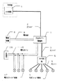
In FIG. 4, one input / output terminal of the optical signal power amplifier 1 'is connected to the
[0003]
Here, the
In general, other devices than the
[0004]
In optical transmission using an optical fiber, signal distortion and attenuation are small, so that it can be used at a long distance. This optical signal power amplifier 1 'is in an optical instrumentation system, and its transmission distance is Used for further extension.
The optical
[0005]
The
Among them, the main role of the optical
[0006]
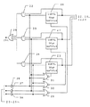
In FIG. 5, the optical
The optical signal transmission /
[0007]
When an optical signal is input from the
[0008]
In general, when such an optical signal power amplifier is installed, the signal transmission form and bit rate in the system are known in advance, so the signal waveform shaping unit 11 receives the signal input from the optical signal transmitting /
Through these series of operations, the optical signal input from the
[0009]
Conversely, when an optical signal is input from the
Due to the above-described action, the optical signal power amplifier 1 'operates as a device that amplifies the power of the optical signal bidirectionally.
[0010]
[Problems to be solved by the invention]
As described above, the main function of the conventional optical signal power amplifier is in the bidirectional optical communication system, which only performs signal waveform distortion shaping and optical signal power amplification. There is no function to connect with. Accordingly, it cannot be used to extend the transmission distance by connecting to a field device compatible with an electric bus.
[0011]
SUMMARY OF THE INVENTION Accordingly, an object of the present invention is to extend the transmission distance of an optical communication system and at the same time extend the transmission distance of an electric communication system, and connect an optical communication system and an electric communication system by interconnecting an optical bus and an electric bus. An object of the present invention is to provide an optical signal power amplifier that can be mixed with a communication system.
[0012]
[Means for Solving the Problems]
In order to solve the above-mentioned problems, an optical signal power amplifier according to
[0013]
In addition, as described in
[0014]
DETAILED DESCRIPTION OF THE INVENTION
Hereinafter, embodiments of the present invention will be described with reference to the drawings.
First, FIG. 1 is an explanatory diagram showing an example of use of the optical
[0015]
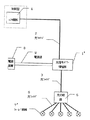
In FIG. 1, one optical signal input / output terminal of an optical
[0016]
In FIG. 2, power is supplied to the optical
[0017]
Since the bus
[0018]
An electrical signal transmission /
[0019]
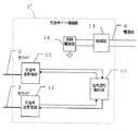
Since the reception outputs of the two optical signal transmission /
[0020]
In FIG. 3, the electrical signal input to the
For this reason, the other retriggerable one-
[0021]
On the other hand, since a signal in the operation direction is continuously supplied from the NOR
The retriggerable one-shot multivibrator is provided for the purpose of extending the signal time and not accepting input from other receiving terminals during that time. it is also possible to carry out the time extension.
[0022]
As described above, the signal from other than the receiving terminal to which the signal is first input by the transmission
A signal synchronized with the signal input from the AND
[0023]
Since one of the inputs of the AND
Here, the transmission
[0024]
The optical signal input from the
[0025]
In addition, when an optical signal is input from the
As is apparent from the above description, the optical
[0026]
【The invention's effect】
As described above, according to the present invention, it is possible to extend the transmission distance of the optical communication system and at the same time extend the transmission distance of the electric communication system, and to mix the optical communication system and the electric communication system. can do.
In addition, since the transmission path extended by the optical signal power amplifier of the present invention is a communication path using light as a medium, the system is more reliable against accidents such as lightning and noise than extending the electric bus. Can be built.
[Brief description of the drawings]
FIG. 1 is an explanatory diagram showing an example of use of an embodiment of the present invention.
FIG. 2 is a block diagram showing an internal configuration of the embodiment of the present invention.
3 is a circuit configuration diagram of a sending direction selection unit in FIG. 2;
FIG. 4 is an explanatory diagram showing an example of use of the prior art.
FIG. 5 is a block diagram showing an internal configuration of a conventional technique.
[Explanation of symbols]
DESCRIPTION OF
Claims (2)
電源に信号を重畳する2線の電気式バス電源を、外部から入力される元電源から生成する電源部と、
電気式バスに接続されて電気式バス信号波形を整形する終端器と、
前記電気式バスとの間で電気信号を送受信する電気信号送受信部と、
この電気信号送受信部と前記2つの光信号送受信部との中で最初に信号を受信した送受信部を判別し、この送受信部以外の送受信部に波形整形後の信号を送出する送出方向選択・波形整形手段と、
を備えたことを特徴とする光信号パワー増幅器。Two optical signal transmission / reception units composed of a reception unit that converts an optical signal into an electrical signal and a transmission unit that converts the electrical signal into an optical signal and sends it out, and amplifies the electrical signal received and converted by these optical signal transmission / reception units And a signal waveform shaping unit that shapes the waveform, and the signal waveform shaping unit amplifies the power of the optical signal input from one optical signal transmission / reception unit to a specified level, and shapes the waveform to the other optical signal. in the bidirectional optical signal power amplifier output from the transceiver unit,
A power supply unit for generating a two-wire electric bus power supply for superimposing a signal on the power supply from an original power supply input from the outside;
A terminator connected to the electrical bus to shape the electrical bus signal waveform;
An electrical signal transmitting and receiving unit for transmitting and receiving electrical signals to and from the electrical bus;
Sending direction selection / waveform for discriminating a transmitting / receiving unit that first receives a signal between the electric signal transmitting / receiving unit and the two optical signal transmitting / receiving units, and sending a signal after waveform shaping to a transmitting / receiving unit other than the transmitting / receiving unit Shaping means;
Optical signal power amplifier, characterized in that it comprises a.
2つの光信号送受信部のうち一方は光ファイバを介してホスト機器に接続され、他方は光ファイバを介して光フィールド機器に接続されるとともに、電気信号送受信部は電気式バスを介して電気式フィールド機器に接続されることを特徴とする光信号パワー増幅器。In the optical signal power amplifier according to claim 1,
One of the two optical signal transmission / reception units is connected to a host device via an optical fiber, the other is connected to an optical field device via an optical fiber, and the electric signal transmission / reception unit is electrically connected via an electric bus. An optical signal power amplifier connected to a field device.
Priority Applications (1)
| Application Number | Priority Date | Filing Date | Title |
|---|---|---|---|
| JP23835398A JP3666552B2 (en) | 1998-08-25 | 1998-08-25 | Optical signal power amplifier |
Applications Claiming Priority (1)
| Application Number | Priority Date | Filing Date | Title |
|---|---|---|---|
| JP23835398A JP3666552B2 (en) | 1998-08-25 | 1998-08-25 | Optical signal power amplifier |
Publications (2)
| Publication Number | Publication Date |
|---|---|
| JP2000068941A JP2000068941A (en) | 2000-03-03 |
| JP3666552B2 true JP3666552B2 (en) | 2005-06-29 |
Family
ID=17028941
Family Applications (1)
| Application Number | Title | Priority Date | Filing Date |
|---|---|---|---|
| JP23835398A Expired - Fee Related JP3666552B2 (en) | 1998-08-25 | 1998-08-25 | Optical signal power amplifier |
Country Status (1)
| Country | Link |
|---|---|
| JP (1) | JP3666552B2 (en) |
-
1998
- 1998-08-25 JP JP23835398A patent/JP3666552B2/en not_active Expired - Fee Related
Also Published As
| Publication number | Publication date |
|---|---|
| JP2000068941A (en) | 2000-03-03 |
Similar Documents
| Publication | Publication Date | Title |
|---|---|---|
| JPS60160231A (en) | Loop form optical dataway system | |
| JPS62200929A (en) | Bias controller for light emitting device of data transmitter for burst communication of fiber optics communication | |
| JPS63279635A (en) | Interface module for electric and optical local area network | |
| EP1451953B1 (en) | An interface device for a fiberoptic communication network and methods of using such a device | |
| JP3666552B2 (en) | Optical signal power amplifier | |
| JP3378969B2 (en) | Receiving system | |
| EP0431654B1 (en) | Adapter for amplified optical lines | |
| CN110943781A (en) | Mode conversion equipment for single-mode optical fiber and multimode optical fiber | |
| US5068847A (en) | Fiber optic network architecture having data feedback for monitoring communications thereon | |
| KR100331301B1 (en) | Data communication apparatus and method | |
| JPH08274719A (en) | Optical output control circuit of optical communication system | |
| JP2786097B2 (en) | Optical subscriber system | |
| CN210780807U (en) | An optical access network device | |
| JPS5981935A (en) | Compound optical communication system | |
| JPH11164483A (en) | Inverter operating device for power equipment | |
| WO2024082204A1 (en) | Lightweight electronic control system for high-reliability and high-safety use | |
| JPS6187439A (en) | Onboard data transmission network | |
| JPS63268394A (en) | Signal amplifier | |
| JPS628627A (en) | Optical communication system for building management system | |
| JPH09284229A (en) | Closed space optical transmission system | |
| JPH0298230A (en) | Method and system for optical transmission system | |
| JPS63164635A (en) | Signal converting device for lighting line carrier system and communication system using the same | |
| JPH01238330A (en) | Optical transmission equipment | |
| JPS60226222A (en) | Method and apparatus of optical space propagation compression communication | |
| JPH05276123A (en) | Optical transceiver |
Legal Events
| Date | Code | Title | Description |
|---|---|---|---|
| A977 | Report on retrieval |
Free format text: JAPANESE INTERMEDIATE CODE: A971007 Effective date: 20041110 |
|
| A131 | Notification of reasons for refusal |
Free format text: JAPANESE INTERMEDIATE CODE: A131 Effective date: 20041216 |
|
| TRDD | Decision of grant or rejection written | ||
| A01 | Written decision to grant a patent or to grant a registration (utility model) |
Free format text: JAPANESE INTERMEDIATE CODE: A01 Effective date: 20050316 |
|
| A61 | First payment of annual fees (during grant procedure) |
Free format text: JAPANESE INTERMEDIATE CODE: A61 Effective date: 20050329 |
|
| R150 | Certificate of patent or registration of utility model |
Free format text: JAPANESE INTERMEDIATE CODE: R150 |
|
| LAPS | Cancellation because of no payment of annual fees |