JP3665520B2 - Liquid crystal display element control device for electronic still camera - Google Patents
Liquid crystal display element control device for electronic still camera Download PDFInfo
- Publication number
- JP3665520B2 JP3665520B2 JP26990499A JP26990499A JP3665520B2 JP 3665520 B2 JP3665520 B2 JP 3665520B2 JP 26990499 A JP26990499 A JP 26990499A JP 26990499 A JP26990499 A JP 26990499A JP 3665520 B2 JP3665520 B2 JP 3665520B2
- Authority
- JP
- Japan
- Prior art keywords
- liquid crystal
- display element
- crystal display
- output value
- luminance
- Prior art date
- Legal status (The legal status is an assumption and is not a legal conclusion. Google has not performed a legal analysis and makes no representation as to the accuracy of the status listed.)
- Expired - Fee Related
Links
Images


Landscapes
- Liquid Crystal (AREA)
- Liquid Crystal Display Device Control (AREA)
- Control Of Indicators Other Than Cathode Ray Tubes (AREA)
- Studio Devices (AREA)
- Devices For Indicating Variable Information By Combining Individual Elements (AREA)
Description
【0001】
【発明の属する技術分野】
本発明は電子スチルカメラに関し、より詳しくは、カメラ本体の背面に設けられた液晶表示素子に関する。
【0002】
【従来の技術】
従来電子スチルカメラにおいて、撮影光学系を介して得られた画像を表示するための液晶表示素子(液晶パネル)がカメラ本体の背面に設けられたものが知られている。電子スチルカメラは通常、光学ファインダを備えており、液晶表示素子には、光学ファインダを介して観察され、撮影された静止画像を表示することができる。さらに、液晶表示装置に光学ファインダを介して観察されるのと同じ画像を動画として表示することのできる電子スチルカメラもあり、この場合は、撮影者は光学ファインダと液晶表示素子のいずれかを見ながら撮影画像を決定することができる。
【0003】
【発明が解決しようとする課題】
液晶表示素子が駆動され、点灯している状態で光学ファインダを覗くと、撮影者は目の下方において液晶表示素子から照射される光を眩しく感じ、光学ファインダが見にくくなるという問題がある。一方、周囲が暗い状態で液晶表示素子を観察するとき、液晶表示素子の輝度が相対的に高くなるために眩しく感じ、液晶表示素子の表示画像が認識しにくくなることがある。また、これとは逆に周囲が明るいとき、液晶表示素子の輝度が相対的に低くなるために表示画像が認識しにくくなることもある。
【0004】
本発明は、液晶表示素子の存在のために光学ファインダが見にくくなったり、また周囲の状況によって液晶表示素子の表示画像が見にくくなったりすることを防止することを目的としている。
【0005】
【課題を解決するための手段】
本発明に係る電子スチルカメラの液晶表示素子制御装置は、カメラ本体の前面に設けられた前面測光センサと、カメラ本体の背面に設けられた背面測光センサと、前面および背面測光センサの出力値に応じて液晶表示素子の輝度を制御する輝度制御手段とを備えることを特徴としている。
【0006】
輝度制御手段は、液晶表示素子のバックライトの輝度を制御することが好ましい。
【0007】
輝度制御手段は、前面測光センサの出力値が背面測光センサの出力値よりも大きいとき、バックライトの輝度を所定値よりも低くする。この場合、輝度制御手段はバックライトを消灯してもよい。
【0008】
輝度制御手段は、前面測光センサの出力値が背面測光センサの出力値よりも小さいとき、バックライトの輝度を所定値よりも高くする。
【0009】
輝度制御手段は、前面測光センサの出力値が背面測光センサの出力値と略等しく、かつ背面測光センサの出力値が第1の基準値よりも小さいとき、バックライトの輝度を所定値よりも低くする。これに対し、前面測光センサの出力値が背面測光センサの出力値と略等しく、かつ背面測光センサの出力値が第2の基準値よりも大きいとき、輝度制御手段はバックライトの輝度を所定値よりも高くする。
【0010】
【発明の実施の形態】
以下、本発明の実施形態を図面を参照して説明する。
図1および図2は、本発明の一実施形態を適用した電子スチルカメラの斜視図である。
【0011】
この電子スチルカメラは一眼レフカメラであり、交換レンズ11はカメラ本体90に着脱自在に取り付けられる。カメラ本体90の上部の中央には光学ファインダ91が設けられ、背面92の略中央には液晶パネル(液晶表示素子)46が設けられている。液晶パネル46では、撮影レンズである交換レンズ11によって得られ、撮影動作によってメモリ(図示せず)に格納された被写体像(静止画像)が表示可能である。
【0012】
カメラ本体90を背面92側から見たとき、カメラ本体90の上部の右側にはシャッタ釦93と状態表示装置55が設けられている。状態表示装置55は液晶表示素子から構成され、この液晶表示素子には電子スチルカメラの種々の設定状態が文字または記号として表示される。
【0013】
カメラ本体90の前面の上部には前面測光センサ94が設けられ、背面の上部には背面測光センサ95が設けられている。第1および背面測光センサ94、95は、それぞれカメラの前方および後方を向いている。すなわち前面測光センサ94はカメラの前方の明るさを検出し、背面測光センサ95はカメラの後方の明るさを検出する。
【0014】
カメラ本体90の側面にはカードスロット96が形成されている。カードスロット96はPCカード(メモリカード)をカメラ本体90内に挿入するために設けられ、カードスロット96の内部にはPCカードが装着されるカードコネクタ(図示せず)が設けられている。
【0015】
図3は電子スチルカメラの主に電気的構成を示すブロック図である。
交換レンズ11はマウントピン12、13を介して、カメラ本体90(図1および図2)内に設けられた電気回路と電気的に接続される。交換レンズ11のレンズ鏡筒内には前群レンズ14と後群レンズ15が設けられ、これらのレンズ14、15の間には絞り16が配設されている。各レンズ14、15はレンズ制御回路17の制御によって光軸方向に変位し、焦点調節が行なわれる。レンズ制御回路17は、カメラ本体内に設けられたシステムコントローラ31からマウントピン12を介して送られてくる制御信号に従って動作する。絞り16は、カメラ本体内に設けられた絞り駆動回路32からマウントピン13を介して送られてくる制御信号に従って動作し、絞り16の開度が調節される。絞り駆動回路32はシステムコントローラ31によって制御される。
【0016】
カメラ本体内において、レンズ14、15の光軸上には、クイックリターンミラー21が設けられている。クイックリターンミラー21は、図示された傾斜状態と上方へ回動した水平状態との間において回動自在である。クイックリターンミラー21の上方にはピント板22が設けられ、ピント板22の上方にはペンタプリズム23が設けられている。ペンタプリズム23の後方にはファインダの接眼レンズ24が配設されている。
【0017】
クイックリターンミラー21の後方には、シャッタ25が設けられ、シャッタ25の後方には赤外カットフィルタ26と光学ローパスフィルタ27が設けられている。光学ローパスフィルタ27の後方にはCCD(撮像素子)33が設けられている。すなわち、クイックリターンミラー21、シャッタ25、赤外カットフィルタ26、光学ローパスフィルタ27、CCD33は、レンズ14、15の光軸上に配置されている。
【0018】
クイックリターンミラー21の回転動作はミラー駆動回路34によって駆動され、シャッタ25の開閉動作はシャッタ駆動回路35によって駆動される。ミラー駆動回路34とシャッタ駆動回路35はシステムコントローラ31によって制御される。
【0019】
通常、ミラー21は傾斜状態に定められており、交換レンズ11から取込まれた光をペンタプリズム23側に導く。このときシャッタ25は閉じており、CCD33に向かう光路を閉塞している。これに対し撮影が行なわれる時、ミラー21はミラー駆動回路34の制御により上方に回動せしめられ、水平状態となる。このミラー21の回動にともない、シャッタ25はシャッタ駆動回路35の制御により開口せしめられ、交換レンズ11から取込まれた光はCCD33の受光面に照射される。すなわち、受光面にはレンズ14、15によって得られた画像が形成され、CCD33では、画像に対応した撮像信号が生成される。
【0020】
システムコントローラ31にはパルス信号発生回路(PPG)36が接続され、パルス信号発生回路36はシステムコントローラ31の制御によって種々のパルス信号を発生する。これらのパルス信号に基づいて、CCD駆動回路37とA/D変換器38と画像信号処理回路39とが駆動され、CCD駆動回路37によりCCD33の動作が制御される。すなわちCCD33から読み出された撮像信号は、A/D変換器38によってデジタル信号に変換され、画像信号処理回路39において、所定の画像処理を施される。画像信号処理回路39には、1つの画像に対応したデジタルの画像データを格納するために十分な容量を有するメモリ40が接続されている。
【0021】
また画像信号処理回路39には、モニタインターフェース41とカードインターフェース42とが接続されている。これらのインターフェース41、42はシステムコントローラ31によって制御される。
【0022】
モニタインターフェース41には、液晶駆動回路44を介してバックライト45と液晶パネル46が接続されている。液晶パネル46では、前述したように、CCD33から読み出された撮像信号に基づいて液晶駆動回路44が制御されることにより、交換レンズ11によって得られた画像が撮影直後にメモリ40に格納された画像データに基づいて、あるいはPCカード43から読み出された画像データに基づいて、液晶駆動回路44が制御され、静止画像が表示される。カードインターフェース42にはカードコネクタ47が接続され、カードコネクタ47にはPCカード43が装着可能である。
【0023】
システムコントローラ31には、AFセンサ51と測光センサ52が接続されている。AFセンサ51は従来公知の構成を有し、AFセンサ51によって、レンズ14、15の焦点調節状態が測定される。測光センサ52によって、露光時の絞り16の開度とCCD33における電荷蓄積時間(露光時間)とを決定するための測光が行なわれる。
【0024】
またシステムコントローラ31には、測光スイッチ53とレリーズスイッチ54と状態表示装置55が接続されている。測光スイッチ53はシャッタ釦93を半押しすることによってオン状態となり、これにより、測光センサ52によって測光が行なわれる。レリーズスイッチ54はシャッタ釦93を全押しすることによってオン状態となり、これにより、シャッタ25が開閉駆動される。すなわちCCD33が露光され、CCD33には画像に対応した撮像信号が発生する。
【0025】
さらにシステムコントローラ31には、前面測光センサ94と背面測光センサ95とが接続されている。
【0026】
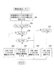
図4は、第1の実施形態において、液晶パネル46のバックライト45の輝度を制御する輝度制御ルーチンのフローチャートである。輝度制御ルーチンは、カメラのメインスイッチがオン状態に定められて各電気回路に電力が供給されたときに起動する。
【0027】
ステップ101では、前面測光センサ94の出力値(または前面光量測定値)Sfoと背面測光センサ95の出力値(または背面光量測定値)Sboが読み取られる。ステップ102では、出力値Sfo、Sboの差の絶対値と許容誤差ΔSが比較される。
【0028】
ステップ102において出力値Sfo、Sboの差の絶対値が許容誤差ΔSよりも大きいと判定されたとき、すなわち出力値Sfo、Sboとが実質的に異なるとき、ステップ103において、前面測光センサの出力値Sfoが背面測光センサの出力値Sboよりも大きいか否かが判定される。出力値Sfoが出力値Sboよりも大きいとき、ステップ104において、液晶駆動回路44を介してバックライト45の輝度が所定値よりも小さくなるように制御され、このルーチンは終了する。
【0029】
このようにステップ102、103、104の順に実行されるのは、カメラ本体90の前方に対して後方が実質的に暗いときであり、典型的には、光学ファインダ91を覗くために、撮影者がカメラ本体90の背面92に顔を近づけたときである。すなわち、この場合、液晶パネル46の輝度が下がるので、撮影者は光学ファインダ91を覗いているとき、液晶パネル46の光を眩しく感じることがない。
【0030】
一方ステップ103において、前面測光センサの出力値Sfoが背面測光センサの出力値Sbo以下であると判定されたとき、ステップ105が実行されてバックライト45の輝度が所定値よりも大きくなるように制御され、輝度制御ルーチンは終了する。これは、カメラ本体90の前方に対して後方が実質的に明るいときであり、例えばカメラ本体90の背面に太陽光等の照明光が当ったときである。このような場合、液晶パネル46の表示画像は照明光のために不鮮明になりやすいが、本実施形態によれば、液晶パネル46の輝度が上がるので表示画像は鮮明になる。
【0031】
ステップ102において出力値Sfo、Sboの差の絶対値が許容誤差ΔS以下であると判定されたとき、すなわち出力値Sfo、Sboとが略等しいとき、ステップ106において、背面測光センサの出力値Sboが第1の基準値SLよりも小さいか否かが判定される。出力値Sfoが第1の基準値SLよりも小さいとき、ステップ104が実行され、バックライト45の輝度が所定値よりも小さくなるように制御される。
【0032】
このようにステップ102、106、104の順に実行されるのは、電子スチルカメラの周囲が全体的に暗いときであり、このような場合、液晶パネル46の輝度が相対的に高くなるために眩しく感じ、液晶パネル46の表示画像が認識しにくくなることがあるが、本実施形態では液晶パネル46の輝度が下げられるので、表示画像は見やすくなる。
【0033】
ステップ106において背面測光センサの出力値Sboが第1の基準値SL以上であると判定されたとき、ステップ107が実行され、背面測光センサの出力値Sboが第2の基準値SHよりも大きいか否かが判定される。出力値Sboが第2の基準値SHよりも大きいとき、ステップ105が実行され、液晶パネル46の輝度は所定値よりも大きくなるように制御される。これは、電子スチルカメラの周囲が全体的に明るい場合であり、液晶パネル46の輝度が相対的に低くなるために液晶パネル46の表示画像が認識しにくくなりやすいが、本実施形態によれば、液晶パネル46の輝度が上がるので表示画像は見やすくなる。
【0034】
ステップ107において背面測光センサの出力値Sboが第2の基準値SHよりも大きいと判定されたとき、ステップ108が実行される。これは、電子スチルカメラの周囲が適度な明るさであり、かつ前面側と背面側の明るさが略等しい場合であり、液晶パネル46のバックライト45の輝度は標準値に定められる。
【0035】
以上のように第1の実施形態によれば、光学ファインダを覗くときに液晶パネルからの光によって光学ファインダが見にくくなったり、周囲の光線の状態によって液晶パネルの表示画像が見にくくなることが防止される。
【0036】
図5は、第2の実施形態において、液晶パネル46のバックライト45の輝度を制御する輝度制御ルーチンのフローチャートである。その他の構成は図1〜図3に示される第1の実施形態と同じである。
【0037】
図5のフローチャートにおいて、各ステップに付された参照符号は、図4のフローチャートの対応するステップに「100」を加算して示されている。例えば、図5のステップ201は図4のステップ101に対応する。
【0038】
図5において、第1の実施形態と異なるステップ210のみであり、ステップ203において前面測光センサの出力値Sfoが背面測光センサの出力値Sboよりも大きいと判定されたとき、実行される。ステップ210では、液晶パネル46のバックライト45が消灯され、輝度制御ルーチンは終了する。その他の動作は図4に示される第1の実施形態と同様である。
【0039】
すなわち第1の実施形態では、光学ファインダ91を覗くために、撮影者がカメラ本体90の背面92に顔を近づけたとき、液晶パネル46が消灯されるので、撮影者は光学ファインダ91を覗いているとき、液晶パネル46の光を眩しく感じることは全くない。その他の作用効果は第1の実施形態と同様である。
【0040】
なお、前述の実施形態の電子スチルカメラだけでなく、クイックリターンミラーの代わりにハーフミラーを用いる等して、被写体像を撮像素子と光学ファインダとの双方に同時に結像させるようにし、液晶表示装置に光学ファインダを介して観察されるのと同じ画像を動画として表示することを可能とした電子スチルカメラについても、本願発明を適用することができる。
【0041】
【発明の効果】
以上のように本発明によれば、液晶表示素子の存在のために光学ファインダが見にくくなったり、また周囲の状況によって液晶表示素子の表示画像が見にくくなったりすることが防止される。
【図面の簡単な説明】
【図1】本発明の一実施形態である液晶表示素子制御装置を備えた電子スチルカメラを前方から見た斜視図である。
【図2】図1に示す電子スチルカメラを後方から見た斜視図である。
【図3】図1および図2に示す電子スチルカメラの主に電気的構成を示すブロック図である。
【図4】第1の実施形態における、バックライトの輝度を制御する輝度制御ルーチンのフローチャートである。
【図5】第2の実施形態における、バックライトの輝度を制御する輝度制御ルーチンのフローチャートである。
【符号の説明】
33 CCD(撮像素子)
45 バックライト
46 液晶表示素子
90 カメラ本体
92 背面
94 前面測光センサ
95 背面測光センサ[0001]
BACKGROUND OF THE INVENTION
The present invention relates to an electronic still camera, and more particularly to a liquid crystal display element provided on the back surface of a camera body.
[0002]
[Prior art]
2. Description of the Related Art Conventionally, an electronic still camera is known in which a liquid crystal display element (liquid crystal panel) for displaying an image obtained via a photographing optical system is provided on the back of a camera body. An electronic still camera is usually provided with an optical viewfinder, and a still image that is observed and photographed through the optical viewfinder can be displayed on the liquid crystal display element. In addition, there is an electronic still camera that can display the same image that is observed on the liquid crystal display device through the optical viewfinder as a moving image. In this case, the photographer views either the optical viewfinder or the liquid crystal display element. The photographed image can be determined while doing so.
[0003]
[Problems to be solved by the invention]
When the liquid crystal display element is driven and the light is turned on, the photographer feels dazzling light emitted from the liquid crystal display element below the eyes, making it difficult to see the optical viewfinder. On the other hand, when the liquid crystal display element is observed in a dark state, the brightness of the liquid crystal display element is relatively high, so that the display image of the liquid crystal display element may be difficult to recognize. On the other hand, when the surroundings are bright, the brightness of the liquid crystal display element is relatively low, and the display image may be difficult to recognize.
[0004]
An object of the present invention is to prevent an optical finder from being difficult to see due to the presence of a liquid crystal display element, and from preventing a display image of a liquid crystal display element from being difficult to see depending on surrounding conditions.
[0005]
[Means for Solving the Problems]
A liquid crystal display element control device for an electronic still camera according to the present invention includes a front photometric sensor provided on the front surface of the camera body, a back photometric sensor provided on the back surface of the camera body, and output values of the front and back photometric sensors. Accordingly, a luminance control means for controlling the luminance of the liquid crystal display element is provided.
[0006]
The brightness control means preferably controls the brightness of the backlight of the liquid crystal display element.
[0007]
The brightness control means makes the brightness of the backlight lower than a predetermined value when the output value of the front photometry sensor is larger than the output value of the back photometry sensor. In this case, the luminance control means may turn off the backlight.
[0008]
The luminance control means makes the luminance of the backlight higher than a predetermined value when the output value of the front photometric sensor is smaller than the output value of the rear photometric sensor.
[0009]
The luminance control means reduces the luminance of the backlight lower than a predetermined value when the output value of the front photometric sensor is substantially equal to the output value of the rear photometric sensor and the output value of the rear photometric sensor is smaller than the first reference value. To do. On the other hand, when the output value of the front photometric sensor is substantially equal to the output value of the rear photometric sensor and the output value of the rear photometric sensor is larger than the second reference value, the luminance control means sets the luminance of the backlight to a predetermined value. Higher than.
[0010]
DETAILED DESCRIPTION OF THE INVENTION
Hereinafter, embodiments of the present invention will be described with reference to the drawings.
1 and 2 are perspective views of an electronic still camera to which an embodiment of the present invention is applied.
[0011]
This electronic still camera is a single-lens reflex camera, and the
[0012]
When the
[0013]
A front
[0014]
A
[0015]
FIG. 3 is a block diagram mainly showing an electrical configuration of the electronic still camera.
The
[0016]
A
[0017]
A
[0018]
The rotation operation of the
[0019]
Usually, the
[0020]
A pulse signal generation circuit (PPG) 36 is connected to the
[0021]
A monitor interface 41 and a card interface 42 are connected to the image
[0022]
A
[0023]
An
[0024]
The
[0025]
Further, a front
[0026]
FIG. 4 is a flowchart of a luminance control routine for controlling the luminance of the
[0027]
In
[0028]
When it is determined in
[0029]
The
[0030]
On the other hand, when it is determined in
[0031]
When it is determined in
[0032]
The
[0033]
When it is determined in
[0034]
When it is determined in
[0035]
As described above, according to the first embodiment, it is possible to prevent the optical finder from being difficult to see due to the light from the liquid crystal panel when looking into the optical finder, or the display image on the liquid crystal panel from being difficult to see due to the state of surrounding light rays. The
[0036]
FIG. 5 is a flowchart of a brightness control routine for controlling the brightness of the
[0037]
In the flowchart of FIG. 5, the reference numerals given to the respective steps are shown by adding “100” to the corresponding steps of the flowchart of FIG. For example, step 201 in FIG. 5 corresponds to step 101 in FIG.
[0038]
In FIG. 5, only step 210 is different from that of the first embodiment, and is executed when it is determined in
[0039]
That is, in the first embodiment, when the photographer brings his face close to the
[0040]
In addition to the electronic still camera of the above-described embodiment, a liquid crystal display device can form a subject image simultaneously on both the image sensor and the optical viewfinder by using a half mirror instead of the quick return mirror. In addition, the present invention can be applied to an electronic still camera that can display the same image as that observed through the optical viewfinder as a moving image.
[0041]
【The invention's effect】
As described above, according to the present invention, it is possible to prevent the optical finder from being difficult to see due to the presence of the liquid crystal display element, and the display image of the liquid crystal display element from being difficult to see depending on the surrounding conditions.
[Brief description of the drawings]
FIG. 1 is a perspective view of an electronic still camera provided with a liquid crystal display element control device according to an embodiment of the present invention, as viewed from the front.
FIG. 2 is a perspective view of the electronic still camera shown in FIG. 1 as viewed from the rear.
3 is a block diagram mainly showing an electrical configuration of the electronic still camera shown in FIGS. 1 and 2. FIG.
FIG. 4 is a flowchart of a luminance control routine for controlling the luminance of the backlight in the first embodiment.
FIG. 5 is a flowchart of a luminance control routine for controlling the luminance of a backlight in the second embodiment.
[Explanation of symbols]
33 CCD (imaging device)
45
Claims (7)
Priority Applications (1)
| Application Number | Priority Date | Filing Date | Title |
|---|---|---|---|
| JP26990499A JP3665520B2 (en) | 1999-09-24 | 1999-09-24 | Liquid crystal display element control device for electronic still camera |
Applications Claiming Priority (1)
| Application Number | Priority Date | Filing Date | Title |
|---|---|---|---|
| JP26990499A JP3665520B2 (en) | 1999-09-24 | 1999-09-24 | Liquid crystal display element control device for electronic still camera |
Publications (2)
| Publication Number | Publication Date |
|---|---|
| JP2001091921A JP2001091921A (en) | 2001-04-06 |
| JP3665520B2 true JP3665520B2 (en) | 2005-06-29 |
Family
ID=17478848
Family Applications (1)
| Application Number | Title | Priority Date | Filing Date |
|---|---|---|---|
| JP26990499A Expired - Fee Related JP3665520B2 (en) | 1999-09-24 | 1999-09-24 | Liquid crystal display element control device for electronic still camera |
Country Status (1)
| Country | Link |
|---|---|
| JP (1) | JP3665520B2 (en) |
Families Citing this family (11)
| Publication number | Priority date | Publication date | Assignee | Title |
|---|---|---|---|---|
| JP2006106634A (en) * | 2004-10-08 | 2006-04-20 | Sharp Corp | Liquid crystal display apparatus and imaging apparatus |
| JP4604789B2 (en) * | 2005-03-25 | 2011-01-05 | カシオ計算機株式会社 | Electronic viewfinder and electronic camera using the same |
| JP4743868B2 (en) * | 2006-03-20 | 2011-08-10 | 株式会社リコー | Image recording device |
| JP4702263B2 (en) * | 2006-03-24 | 2011-06-15 | ソニー株式会社 | Display device and electronic device |
| JP5061532B2 (en) * | 2006-08-22 | 2012-10-31 | 株式会社ニコン | Electronics |
| JP2008275732A (en) * | 2007-04-26 | 2008-11-13 | Sony Corp | Imaging apparatus |
| JP2009038613A (en) * | 2007-08-02 | 2009-02-19 | Nikon Corp | Imaging apparatus |
| JP2010093392A (en) * | 2008-10-03 | 2010-04-22 | Canon Inc | Imaging apparatus, control method therefor, and program |
| JP5253130B2 (en) * | 2008-12-19 | 2013-07-31 | キヤノン株式会社 | Image display device, imaging device, and image display method |
| JP5663914B2 (en) * | 2010-03-25 | 2015-02-04 | 株式会社ニコン | Image display device |
| CN105244006B (en) * | 2014-07-31 | 2018-02-23 | 维沃移动通信有限公司 | The backlight adjusting method and its display device of a kind of display device |
-
1999
- 1999-09-24 JP JP26990499A patent/JP3665520B2/en not_active Expired - Fee Related
Also Published As
| Publication number | Publication date |
|---|---|
| JP2001091921A (en) | 2001-04-06 |
Similar Documents
| Publication | Publication Date | Title |
|---|---|---|
| CN100458553C (en) | Image taking apparatus and lens apparatus | |
| US7583892B2 (en) | Finder device and camera | |
| US6839087B1 (en) | Exposure controller of a digital camera | |
| JP3665520B2 (en) | Liquid crystal display element control device for electronic still camera | |
| US6798456B1 (en) | Exposure period control device for electronic still camera | |
| JP2008170872A (en) | Imaging apparatus | |
| JP2004104673A (en) | Digital camera | |
| JP4253086B2 (en) | Electronic still camera shooting operation control device | |
| JP2006339902A (en) | Finder and camera | |
| US7573512B2 (en) | Recording operation control device for electronic still camera | |
| JP4347958B2 (en) | Exposure control device for electronic still camera | |
| JP5532565B2 (en) | camera | |
| JP4105933B2 (en) | Digital camera and image generation method | |
| JP4645431B2 (en) | camera | |
| JP2001078083A (en) | Exposure time controller for electronic still camera | |
| JP3843001B2 (en) | Interchangeable lens SLR digital camera | |
| JP4446517B2 (en) | Electronic camera white balance control device and remote controller | |
| JP3887144B2 (en) | Light source selection device for electronic still camera | |
| JP3939899B2 (en) | White balance adjustment device for electronic still camera | |
| JP2001318406A (en) | Camera with lens cover | |
| JP4136331B2 (en) | Operation control device for digital still camera | |
| KR20080090022A (en) | Photographing apparatus, and photographing method | |
| JP2001318415A (en) | Camera provided with previewing function | |
| KR20100003639A (en) | Apparatus for digital picturing image | |
| JP2003153074A (en) | Digital camera |
Legal Events
| Date | Code | Title | Description |
|---|---|---|---|
| A977 | Report on retrieval |
Free format text: JAPANESE INTERMEDIATE CODE: A971007 Effective date: 20050304 |
|
| TRDD | Decision of grant or rejection written | ||
| A01 | Written decision to grant a patent or to grant a registration (utility model) |
Free format text: JAPANESE INTERMEDIATE CODE: A01 Effective date: 20050316 |
|
| A61 | First payment of annual fees (during grant procedure) |
Free format text: JAPANESE INTERMEDIATE CODE: A61 Effective date: 20050401 |
|
| R150 | Certificate of patent or registration of utility model |
Free format text: JAPANESE INTERMEDIATE CODE: R150 |
|
| FPAY | Renewal fee payment (event date is renewal date of database) |
Free format text: PAYMENT UNTIL: 20090408 Year of fee payment: 4 |
|
| FPAY | Renewal fee payment (event date is renewal date of database) |
Free format text: PAYMENT UNTIL: 20100408 Year of fee payment: 5 |
|
| FPAY | Renewal fee payment (event date is renewal date of database) |
Free format text: PAYMENT UNTIL: 20100408 Year of fee payment: 5 |
|
| FPAY | Renewal fee payment (event date is renewal date of database) |
Free format text: PAYMENT UNTIL: 20110408 Year of fee payment: 6 |
|
| FPAY | Renewal fee payment (event date is renewal date of database) |
Free format text: PAYMENT UNTIL: 20110408 Year of fee payment: 6 |
|
| FPAY | Renewal fee payment (event date is renewal date of database) |
Free format text: PAYMENT UNTIL: 20120408 Year of fee payment: 7 |
|
| FPAY | Renewal fee payment (event date is renewal date of database) |
Free format text: PAYMENT UNTIL: 20120408 Year of fee payment: 7 |
|
| S111 | Request for change of ownership or part of ownership |
Free format text: JAPANESE INTERMEDIATE CODE: R313111 |
|
| FPAY | Renewal fee payment (event date is renewal date of database) |
Free format text: PAYMENT UNTIL: 20120408 Year of fee payment: 7 |
|
| R350 | Written notification of registration of transfer |
Free format text: JAPANESE INTERMEDIATE CODE: R350 |
|
| FPAY | Renewal fee payment (event date is renewal date of database) |
Free format text: PAYMENT UNTIL: 20130408 Year of fee payment: 8 |
|
| FPAY | Renewal fee payment (event date is renewal date of database) |
Free format text: PAYMENT UNTIL: 20140408 Year of fee payment: 9 |
|
| S533 | Written request for registration of change of name |
Free format text: JAPANESE INTERMEDIATE CODE: R313533 |
|
| R350 | Written notification of registration of transfer |
Free format text: JAPANESE INTERMEDIATE CODE: R350 |
|
| LAPS | Cancellation because of no payment of annual fees |