JP3664743B2 - Burn-in board - Google Patents
Burn-in board Download PDFInfo
- Publication number
- JP3664743B2 JP3664743B2 JP29360393A JP29360393A JP3664743B2 JP 3664743 B2 JP3664743 B2 JP 3664743B2 JP 29360393 A JP29360393 A JP 29360393A JP 29360393 A JP29360393 A JP 29360393A JP 3664743 B2 JP3664743 B2 JP 3664743B2
- Authority
- JP
- Japan
- Prior art keywords
- lead
- substrate
- board
- burn
- lead holes
- Prior art date
- Legal status (The legal status is an assumption and is not a legal conclusion. Google has not performed a legal analysis and makes no representation as to the accuracy of the status listed.)
- Expired - Lifetime
Links
Images


Landscapes
- Multi-Conductor Connections (AREA)
- Coupling Device And Connection With Printed Circuit (AREA)
- Testing Of Individual Semiconductor Devices (AREA)
- Testing Or Measuring Of Semiconductors Or The Like (AREA)
Description
【0001】
【産業上の利用分野】
本発明は、半導体装置の試験に使用されるバーンインボードに関する。
【0002】
近年、半導体装置はゲートアレイ型の多ピン化、高速化に伴い高発熱デバイスが増加すると共に、小型化が要求されてパッケージピンの狭ピッチ化が進んでいる。これにより、製造時の種々なプロセス障害やアセンブリ障害が増えており、バーンインを行う必要がでてきている。
【0003】
また、同一のパッケージで電源ピンの配置が異なるデバイスが増えてきており、バーンイン時に使用するバーンインボードの多層化を余儀なくされてデバイスの供給納期の短縮に沿えずその対応が要求されている。
【0004】
このため、実装個数を減少させずに特性を維持するバーンインボードを提供する必要がある。
【0005】
【従来の技術】
半導体装置の多ピン化が進むと、そのパッケージがPGA(Pin Grid Array)型となり、バーンインを行うためのバーンインボードもこれに応じて多層化される。そして、ピンの狭ピッチによるノイズ緩和のために、各層毎にグランド(GND)を介在させている。
【0006】
例えば、ピンが0.3 mmピッチで配列されたPGA型の半導体装置用のバーンインボードは6層で構成され、ピン配列が水平垂直で100ミル(2.54mm)、対角で約70ミル(1.796mm )のPGA型の半導体装置用のバーンインボードは10層で構成される。
【0007】
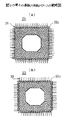
そこで、図10に、従来のバーンインボードのパターン構成図を示す。図10(A),(B)はバーンインボード上の半導体装置が挿入されるICソケットの複数のフットパターンのうちの一つであり、図10(A)は6層(母体基板上に5層)の場合を示しており、図10(B)は10層(母体基板上に9層)の場合を示している。
【0008】
図10(A)において、4つの領域11a〜11dのそれぞれに規則的に0.3 mmピッチでピンパターン(例えばφ0.7 mm)12が配列されて形成されており、外側2列が1層目で引き出しパターン13aが形成され、順次1列ごとに2層目から5層目で引き出しパターン13b〜13eが形成される。これら引き出しパターン13a〜13eはピンパターン12間で1本形成される。
【0009】
そして、ピンパターン12にICソケットのピンが挿入され、半田接続される。
【0010】
また、図10(B)において、空領域14の周囲にピンパターン15が水平垂直100ミル、対角約70ミルのピッチで配列される。そして、外側2列が1層目で引き出しパターン16a(例えば、幅0.35mm,以下同じ)が形成され、順次2層目から8層目まで1列ごとに引き出しパターン16a〜16hが形成されると共に、内側2列が9層目で引き出しパターン16iが形成される。この場合も引き出しパターン16a〜16iはピンパターン15間で1本形成される。
【0011】
従って、通常6層目から9層目までのピンパターン15が電源ピンとして割り当てた場合に、電源パターンとなる引き出しパターン16f〜16iの幅が信号用の引き出しパターン16a〜16eと同様の例えば0.35mmとなる。
【0012】
【発明が解決しようとする課題】
しかし、上述のように、よりピンの狭ピッチ、高発熱デバイス用のバーンインボードを製作する場合、ボードの積層数を増加して、電源層を増加させるが、又はデバイスの実装個数を減少させるかの対応しかとることができず、製造工程の増加やバーンインボードの個数の増加を招きコスト高になるという問題がある。また、バーンインボードを多層板化するとリピート製作時に日数を要するという問題がある。
【0013】
さらに、電源用の引き出しパターン16f〜16iを信号用の引き出しパターン16a〜16eと同じ幅でしか形成することができないことから、電源電流変動によるノイズの影響を受け易いという問題がある。
【0014】
そこで、本発明は上記課題に鑑みなされたもので、ノイズ干渉の低減、低コスト化を図り、製造容易とするバーンインボードを提供することを目的とする。
【0015】
【課題を解決するための手段】
上記課題は、バーンインが行われる、PGA型の半導体デバイスを保持する所定数の保持部の、下方に延出する複数のリードピンの挿入されるリード孔が形成され、該リード孔に対応する配線パターンが形成されるバーンインボードにおいて、前記保持部を実装するためのものであって、総ての前記リード孔が形成されると共に、該リード孔のうち所定列のリード孔に対応する前記配線パターンが両面のそれぞれに形成され、該配線パターンが形成されたリード孔に対応する前記リードピンが不要長さ部分を切断除去されて挿入され接続固定される第1の基板と、該リードピン挿入方向で該第1の基板に重ねられて配置されるものであって、該第1の基板の該配線パターンが形成された該リード孔を除く前記リード孔が形成されると共に、形成された該リード孔のうち総ての又は所定列のリード孔に対応する前記配線パターンが両面のそれぞれに形成され、該配線パターンが形成されたリード孔に対応する前記リードピンが不要長さ部分を切断除去されて挿入され接続固定される第2の基板と、を有して構成することにより解決される。
【0016】
また、前記保持部のリードピンの個数に応じて前記第2の基板の下方に所定枚数重ねられて配置される基板であって、上方に位置される所定数の基板に前記配線パターンが形成されたリード孔を除く前記リード孔が形成されると共に、形成された該リード孔のうち総ての又は所定列のリード孔に対応する前記配線パターンが両面のそれぞれに形成され、該配線パターンが形成されたリード孔に対応する前記リードピンが不要長さ部分を切断除去されて挿入され接続固定される。
【0017】
【作用】
上述のように、第1の基板以下に、リードピン挿入方向に所定枚数の基板が重ねられて配置される。これら基板は、上方に位置される基板に挿入されて接続固定されて不要長さ部分を切断除去されたリードピン以外のリードピンに対応するリード孔が形成される。また、リード孔のうち、所定列のリード孔に対応する配線パターンが各基板の両面にそれぞれ形成され、該配線パターンが形成されたリード孔に対応するリードピンが不要長さ部分を切断除去されて挿入され、接続固定されたものである。
【0018】
このように、配線パターンを両面に形成した基板を半導体デバイスに応じて重ねて配置することから、実装個数を減らすことなく、一枚の基板で多層化するよりも低コストかつ製造容易で短期間で製造することが可能になる。また、各基板で信号系と電源系を分離することが可能となり、電源用の配線パターンが十分な太さで形成されて電源電流変動に伴うノイズ干渉を緩和することが可能となる。
【0019】
【実施例】
図1に、本発明の一実施例の構成図を示す。図1(A)において、バーンインボード21は、半導体デバイス(図示せず)を挿入させて保持する保持部であるICソケット22が所定数実装される第1の基板23と、第1の基板23の下方でICソケット22のリードピン(後述する)の挿入方向に第2の基板24から第3の基板25,第4の基板26,第5の基板27まで重ねられて配置される。
【0020】
これら第1〜第5の基板23〜27は、4つのスペーサ28をそれぞれ介在させてネジ29で取り付けられる。また、一端には、電源を供給し、信号の送受を行うためのコネクタ(接続ピンでもよい)30が設けられる。なお、第1〜第5の基板23〜27はそれぞれ両面に配線パターンが形成される(図2〜図6において説明する)。
【0021】
そこで、図1(B)に一つのソケット22の部分の拡大図が示されており、ICソケット22のリードピン31がバーンインボード21に挿入されている。すなわち、第1の基板23には、図1(C)に示すようにICソケット22のリードピン31の総てに対応してリード孔32が形成されており、リードピン31の外側3列のリードピン31aが該第1の基板23に接続固定され、不要な長さ部分が切断除去される。
【0022】
また、リードピン31a以外のリードピン31のさらに外側3列のリードピン31bが第2の基板24に接続固定されて不要な長さ部分が切断除去される。同様の残りのリードピン31のうち外側1列のリードピン31cが第3の基板25に接続固定されて不要な長さ部分が切断除去され、さらに残りのリードピン31のうち外側1列のリードピン31dが第4の基板26に接続固定されて不要な長さ部分が切断除去される。
【0023】
そして、最内側1列のリードピン31eが第5の基板27に接続固定されて不要な長さ部分が切断除去されるものである。
【0024】
ところで、上述のように図1(C)には第1の基板23に形成されたリード孔32が示されており、例えば、白抜き部分を信号系とし、黒塗り部分を電源系とし、電源系のうち最内側の1列をグランド(GND)とする。そこで、図1(B)に示すICソケット22のリードピン31(31a〜31e)に対応させると、外側3列のリード孔32aが当該第1の基板23に接続固定されるリードピン31aに対応する。またリード孔32bが下方に配置される第2の基板24に接続固定されるリードピン31bに対応し、同様にリード孔32cがリードピン31cに、リード孔32dがリードピン31dに、リード孔31eがリードピン31eにそれぞれ対応する。
【0025】
ここで、図1(D)は図1(C)の一部分を示したもので、リード孔32の形成ピッチ、及び配線パターンについて説明する。
【0026】
図1(C),(D)において、リード孔32は例えば水平垂直方向にd1 =100ミル(2.54mm)ピッチであり、対角方向にd2 =約70ミル(1.796 mm)で配列形成される。また、信号系のリード孔32a,32bより引き出される引き出しパターン33は、異なるデバイスによっては、信号系のリード孔32a,32bが電源系となる場合もあり、例えば電源系のリードピン31c,31dで1ピン当たり400mmAの電流が流れるとすると0.4 mm幅(1A当たり1mm)で形成する。従って、引き出しパターン33aを幅0.4 mmで形成した場合、リード孔32a,32bと引き出しパターン33との間隔d4 は0.35mmとなる。
【0027】
そこで、図2〜図6に、図1の第1〜第5の基板の両面パターンの説明図を示す。なお、図2〜図6では、黒塗り部分がパターンの形成されるリード孔として示している。
【0028】
図2は第1の基板23であり、図2(A)は部品面(ICソケット22が実装される面)を示しており、図2(B)ははんだ面(裏面)を示している。すなわち、第1の基板23には、実装されるICソケット22の総てのリードピン31(31a〜31e)に対応するリード孔32(32a〜32e)が形成される。なお、形成されるリード孔32には基板両面ではんだによる接続固定するためのランド部(図示せず)が形成される(以下においても同様である)。
【0029】
図2(A)に示す部品面では外側2列のリード孔32aに信号ラインとなる引き出しパターン33が形成され、図2(B)に示すはんだ面では外側から3列目のリード孔32aに引き出しパターン33が形成される。なお、上述のランド部と引き出しパターンとが基板上の配線パターンとなる。
【0030】
そして、図1(B)に示すように、ICソケット22のリードピン31がリード孔32に挿入され、はんだにより接続固定されると共に、リードピン31aの不要な長さ部分が切断除去されるものである。
【0031】
図3は第2基板24であり、図3(A)が部品面、図3(B)がはんだ面を示している。図3(A),(B)に示される第2の基板24には、上方に位置される第1の基板23で引き出しパターン33が形成されたリード孔32a以外のリード孔32b〜32eが形成される。
【0032】
図3(A)に示す部品面では、外側2列のリード孔32bに信号ラインとなる引き出しパターン33が形成され、図3(B)に示すはんだ面では外側から3列目のリード孔32bに引き出しパターン33が形成される。そして、図1(B)に示すように、ICソケット22のリードピン31bが該引き出しパターン33が形成されたリード孔32bに挿入されて、はんだにより接続固定され、不要な長さ部分が切断除去される。
【0033】
図4は第3基板であり、図4(A)が部品面、図4(B)がはんだ面を示している。図4(A),(B)に示される第3の基板25には、上方に位置された第1及び第2の基板23,24で引き出しパターン33が形成されたリード孔32a,32b以外のリード孔32c〜32eが形成される。
【0034】
図4(A)に示す部品面及び図4(B)に示すはんだ面では外側1列のリード孔32cのみを含んで配線パターンとして電源べた面34がそれぞれ形成される。そして、図1(B)に示すように、ICソケット22のリードピン31cが該電源べた面34が形成されたリード孔32cに挿入されてはんだにより接続固定され、不要な長さ部分が切断除去される。
【0035】
図5は第4基板26であり、図5(A)が部品面、図5(B)がはんだ面を示している。図5(A),(B)に示される第4の基板26には、上方に位置された第1〜第3の基板23〜25で引き出しパターン33が形成されたリード孔32a〜32c以外のリード孔32d,32eが形成される。
【0036】
図5(A)に示す部品面及び図5(B)に示すはんだ面では外側1列のリード孔32dのみを含んで配線パターンとして電源べた面34がそれぞれ形成される。そして、図1(B)に示すように、ICソケット22のリードピン31が該電源べた面34が形成されたリード孔32dに挿入されて、はんだにより接続固定され、不要な長さ部分が切断除去される。
【0037】
図6は第5基板27であり、図6(A)が部品面、図6(B)がはんだ面を示している。図6(A),(B)に示される第5の基板27には、上方に位置された第1〜第4の基板23〜26で引き出しパターン33が形成されたリード孔32a〜32d以外の内側のリード孔32eが形成される。
【0038】
図6(A)に示す部品面及び図6(B)に示すはんだ面では外側1列のリード孔32eのみを含んで配線パターンとして電源べた面34がそれぞれ形成される。
【0039】
そして、図1(B)に示すように、ICソケット22のリードピン31eが該電源べた面34が形成されたリード孔32eに挿入されてはんだにより接続固定されるものである。
【0040】
なお、図2〜図6に示す第1〜第5の基板23〜27で構成されるバーンインボード21にICソケット22を実装するにあたり、第1の基板23にまずICソケット22を挿入してはんだ付けした後にリードピン31aを切断し、次に第2の基板24に残りのリードピン31b〜31eを挿入してはんだ付けした後にリードピン31bを切断するように順次はんだ付けとリード切断を行うことにより実装してもよい。
【0041】
また、第1〜第5の基板23〜27を重ねて組立てておき、一方でICソケット22のリードピン31を予め所定の長さに切断しておいて、当該ICソケット22を重ねられた第1〜第5の基板23〜27のリード孔32a〜32eにそれぞれに挿入して、はんだリフロー等によりはんだ接続をすることにより実装してもよい。
【0042】
このように、多ピン狭ピッチ、高発熱の半導体デバイスのバーンインを行うにあたり、実装個数を減らすことなく両面基板を重ねて配置させることにより、一枚の基板を多層化するよりも低コストかつ製造容易で短期間で製造することができる。また、第1〜第5の基板23〜27で信号系と電源系(グランドGNDを含む)を分離することができ、電源用の配線パターンを電源べた面34で形成することができることにより電源電流変動に伴うノイズ干渉を緩和することができるものである。
【0043】
次に、図7に、本発明の他の実施例の構成図を示す。図7は、バーンインボード21の一部分(ICソケット1個分)を示したもので、それぞれ両面に配線パターン(図8及び図9で説明する)が形成された第1の基板41及び第2の基板42で構成され、これらにICソケット43が実装される。この場合、ICソケット43のリードピン44のうち外側3列のリードピン44aが第1の基板41に挿入されてはんだにより接続固定され、不要な長さ部分が切断除去される。そして、残り3列のリードピン44bが第2の基板42に挿入されてはんだにより接続固定されるものである。
【0044】
これにより、上記実施例と同様に低コストかつ製造容易で短期間で製造することができる。
【0045】
そこで、図8及び図9に、図7の第1及び第2の基板の両面パターンの説明図を示す。
【0046】
図8は第1の基板41であり、図8(A)は部品面、図8(B)ははんだ面を示している。第1の基板41にはICソケット43のリードピン44の総てに対応して4つの領域45a〜45dに例えば0.3 mmピッチで径0.7 mmのリード孔46が形成される。
【0047】
図8(A)の部品面ではリード孔46の外側2列のリード孔46aに配線パターンとして引き出しパターン47がそれぞれ形成され、図8(B)のはんだ面では外側から3列目のリード孔46aに引き出しパターン47が形成される。この両面のリード孔46aがICソケット43のリードピン44aに対応する。
【0048】
すなわち、このリード孔46aにICソケット43のリードピン44aが挿入されてはんだにより接続固定され、不要の長さ部分が切断除去される。
【0049】
図9は第2の基板42であり、図9(A)は部品面、図9(B)ははんだ面を示している。第2の基板42には、4つの領域45a〜45dにおいてICソケット43のリードピン44に対応するリード孔46のうち、第1の基板42で引き出しパターン47が形成されたリード孔46a以外のリード孔46bが形成される。このリード孔46bはICソケット43のリードピン44bに対応する。
【0050】
図9(A)の部品面ではリード孔46bの外側2列のリード孔46bに配線パターンとして引き出しパターン47がそれぞれ形成され、図9(B)のはんだ面では最内側の列のリード孔46bに引き出しパターン47が形成される。
【0051】
そして、このリード孔46bにICソケット43のリードピン44bが挿入されてはんだにより接続固定されるものである。
【0052】
【発明の効果】
以上のように本発明によれば、バーンインを行う半導体デバイスに応じて両面に配線パターンが形成される基板を所定数重ねて配置し、保持部のリードピンを各基板に順次接続固定して不要長さ部分を切断除去させて実装させる構成とすることにより、ノイズ干渉の低減、低コスト化を図ることができると共に、製造容易となって短期間の製造を行うことができるものである。
【図面の簡単な説明】
【図1】本発明の一実施例の構成図である。
【図2】図1の第1の基板の両面パターンの説明図である。
【図3】図1の第2の基板の両面パターンの説明図である。
【図4】図1の第3の基板の両面パターンの説明図である。
【図5】図1の第4の基板の両面パターンの説明図である。
【図6】図1の第5の基板の両面パターンの説明図である。
【図7】本発明の他の実施例の構成図である。
【図8】図7の第1の基板の両面パターンの説明図である。
【図9】図7の第2の基板の両面パターンの説明図である。
【図10】従来のバーンインボードのパターン構成図である。
【符号の説明】
21 バーンインボード
22,43 ICソケット
23,41 第1の基板
24,42 第2の基板
25 第3の基板
26 第4の基板
27 第5の基板
28 スペーサ
29 ネジ
30 コネクタ
31,44 リードピン
32,46 リード孔
33,47 引き出しパターン
34 電源べた面[0001]
[Industrial application fields]
The present invention relates to a burn-in board used for testing a semiconductor device.
[0002]
2. Description of the Related Art In recent years, semiconductor devices have increased in number of high heat generating devices as the number of gate array type pins increases, and the speed has increased, and downsizing of package pins has been progressing in response to demand for miniaturization. As a result, various process failures and assembly failures at the time of manufacture are increasing, and it is necessary to perform burn-in.
[0003]
In addition, devices with different power supply pin arrangements in the same package are increasing, and the burn-in board used at the time of burn-in is forced to be multi-layered, and the response is required without shortening the supply time of the device.
[0004]
Therefore, it is necessary to provide a burn-in board that maintains the characteristics without reducing the number of mounted packages.
[0005]
[Prior art]
As the number of pins of a semiconductor device increases, the package becomes a PGA (Pin Grid Array) type, and a burn-in board for performing burn-in is also multilayered accordingly. In order to mitigate noise due to the narrow pin pitch, a ground (GND) is interposed for each layer.
[0006]
For example, a burn-in board for a PGA type semiconductor device in which pins are arranged at a pitch of 0.3 mm is composed of 6 layers, and the pin arrangement is 100 mils (2.54 mm) horizontally and vertically, and approximately 70 mils (1.796 mm) diagonally. The burn-in board for PGA type semiconductor devices is composed of 10 layers.
[0007]
FIG. 10 shows a pattern configuration diagram of a conventional burn-in board. 10A and 10B show one of a plurality of foot patterns of an IC socket into which a semiconductor device on a burn-in board is inserted. FIG. 10A shows six layers (five layers on a base substrate). 10B shows a case of 10 layers (9 layers on the base substrate).
[0008]
10A, pin patterns (for example, φ0.7 mm) 12 are regularly arranged at a pitch of 0.3 mm in each of the four regions 11a to 11d, and the outer two rows are the first layer. A lead pattern 13a is formed, and
[0009]
Then, the pins of the IC socket are inserted into the
[0010]
In FIG. 10B,
[0011]
Therefore, when the
[0012]
[Problems to be solved by the invention]
However, as mentioned above, when manufacturing burn-in boards for narrow pin pitch and high heat generation devices, increase the number of stacked boards and increase the power supply layer, or reduce the number of devices mounted. However, there is a problem that the manufacturing process is increased and the number of burn-in boards is increased, resulting in an increase in cost. In addition, when the burn-in board is made into a multilayer board, there is a problem that it takes days when producing repeats.
[0013]
Furthermore, since the power supply lead patterns 16f to 16i can be formed only with the same width as the
[0014]
Accordingly, the present invention has been made in view of the above problems, and an object of the present invention is to provide a burn-in board that is easy to manufacture by reducing noise interference and reducing costs.
[0015]
[Means for Solving the Problems]
The above-mentioned problem is that a predetermined number of holding parts for holding a PGA type semiconductor device where burn-in is performed, lead holes into which a plurality of lead pins extending downward are inserted, and wiring patterns corresponding to the lead holes In the burn-in board formed, all the lead holes are formed, and the wiring pattern corresponding to the lead holes in a predetermined row is formed among the lead holes. A first substrate formed on each of the both surfaces and corresponding to the lead hole in which the wiring pattern is formed, the unnecessary length portion being cut and removed, and inserted and fixed; and the first pin in the lead pin insertion direction. The lead hole is formed so as to be superposed on the first substrate, and the lead hole is formed except for the lead hole in which the wiring pattern of the first substrate is formed. The wiring patterns corresponding to all or predetermined rows of the formed lead holes are formed on both surfaces, and the lead pins corresponding to the lead holes formed with the wiring patterns are unnecessary length portions. And the second substrate that is inserted and fixed by being cut and removed.
[0016]
Further, the wiring pattern is formed on a predetermined number of substrates located above the second substrate, the predetermined number being stacked below the second substrate according to the number of lead pins of the holding unit. The lead holes except for the lead holes are formed, and the wiring patterns corresponding to all or predetermined rows of the formed lead holes are formed on both sides, and the wiring patterns are formed. The lead pins corresponding to the lead holes are inserted and fixed by cutting off unnecessary length portions.
[0017]
[Action]
As described above, a predetermined number of substrates are arranged to overlap the first substrate and below in the lead pin insertion direction. These substrates are formed with lead holes corresponding to lead pins other than the lead pins that are inserted into a substrate positioned above, connected and fixed, and unnecessary length portions are cut off. Further, among the lead holes, wiring patterns corresponding to the lead holes in a predetermined row are respectively formed on both surfaces of each substrate, and the lead pins corresponding to the lead holes in which the wiring patterns are formed are cut off and removed by unnecessary length portions. Inserted and connected and fixed.
[0018]
In this way, since the substrates with wiring patterns formed on both sides are arranged according to the semiconductor device, it is cheaper and easier to manufacture than a multi-layer with a single substrate, without reducing the number of mounting, and in a short period of time. It becomes possible to manufacture with. In addition, the signal system and the power supply system can be separated from each other, and the power supply wiring pattern can be formed with a sufficient thickness to mitigate noise interference caused by power supply current fluctuations.
[0019]
【Example】
FIG. 1 shows a configuration diagram of an embodiment of the present invention. In FIG. 1A, a burn-in
[0020]
These first to
[0021]
Therefore, FIG. 1B shows an enlarged view of a portion of one
[0022]
Further, the lead pins 31b in the three outer rows of the lead pins 31 other than the lead pins 31a are connected and fixed to the
[0023]
Then, the innermost one row of
[0024]
Incidentally, as described above, FIG. 1C shows the
[0025]
Here, FIG. 1D shows a part of FIG. 1C, and the formation pitch of the lead holes 32 and the wiring pattern will be described.
[0026]
1 (C) and 1 (D), the lead holes 32 have, for example, a pitch of d 1 = 100 mils (2.54 mm) in the horizontal and vertical directions, and an array formed with d 2 = about 70 mils (1.796 mm) in the diagonal direction. Is done. Further, the
[0027]
2 to 6 are explanatory diagrams of the double-sided patterns of the first to fifth substrates of FIG. 2 to 6, black portions are shown as lead holes in which patterns are formed.
[0028]
FIG. 2 shows the
[0029]
On the component side shown in FIG. 2A,
[0030]
As shown in FIG. 1B, the
[0031]
FIG. 3 shows the
[0032]
In the component surface shown in FIG. 3A, lead-out
[0033]
FIG. 4 shows a third substrate, FIG. 4A shows the component surface, and FIG. 4B shows the solder surface. In the
[0034]
In the component surface shown in FIG. 4A and the solder surface shown in FIG. 4B, a
[0035]
FIG. 5 shows the
[0036]
On the component surface shown in FIG. 5A and the solder surface shown in FIG. 5B, a
[0037]
FIG. 6 shows the
[0038]
In the component surface shown in FIG. 6A and the solder surface shown in FIG. 6B, a
[0039]
As shown in FIG. 1B, the
[0040]
In mounting the
[0041]
In addition, the first to
[0042]
In this way, when performing burn-in of a multi-pin narrow pitch, high heat-generating semiconductor device, it is possible to manufacture at a lower cost than by stacking single substrates by stacking double-sided substrates without reducing the number of mounted devices. It is easy and can be manufactured in a short period of time. Further, the signal system and the power supply system (including the ground GND) can be separated by the first to
[0043]
Next, FIG. 7 shows a configuration diagram of another embodiment of the present invention. FIG. 7 shows a part of the burn-in board 21 (one IC socket), and the
[0044]
Thereby, like the said Example, it can manufacture at low cost, easy manufacture, and a short period of time.
[0045]
8 and 9 are explanatory views of the double-sided patterns of the first and second substrates of FIG.
[0046]
FIG. 8 shows the
[0047]
In the component surface of FIG. 8A,
[0048]
In other words, the lead pin 44a of the
[0049]
FIG. 9 shows the
[0050]
9A,
[0051]
The lead pin 44b of the
[0052]
【The invention's effect】
As described above, according to the present invention, a predetermined number of substrates on which wiring patterns are formed on both sides are arranged in accordance with the semiconductor device to be burned in, and the lead pins of the holding portion are sequentially connected and fixed to each substrate to eliminate unnecessary length. By adopting a configuration in which the portion is cut and removed, the noise interference can be reduced and the cost can be reduced, and the manufacturing can be facilitated and the manufacturing can be performed in a short time.
[Brief description of the drawings]
FIG. 1 is a configuration diagram of an embodiment of the present invention.
FIG. 2 is an explanatory diagram of a double-sided pattern of the first substrate of FIG.
3 is an explanatory diagram of a double-sided pattern of the second substrate of FIG. 1. FIG.
FIG. 4 is an explanatory diagram of a double-sided pattern of the third substrate of FIG.
5 is an explanatory diagram of a double-sided pattern of the fourth substrate in FIG. 1. FIG.
6 is an explanatory diagram of a double-sided pattern of the fifth substrate in FIG. 1. FIG.
FIG. 7 is a configuration diagram of another embodiment of the present invention.
8 is an explanatory diagram of a double-sided pattern of the first substrate of FIG. 7. FIG.
FIG. 9 is an explanatory diagram of a double-sided pattern of the second substrate of FIG.
FIG. 10 is a pattern configuration diagram of a conventional burn-in board.
[Explanation of symbols]
21 Burn-in
Claims (4)
該リードピン挿入方向で該第1の基板(23,41)に重ねられて配置されるものであって、該第1の基板(23,41)の該配線パターン(33,47)が形成された該リード孔(32a,46a)を除く前記リード孔が形成されると共に、形成された該リード孔のうち総ての又は所定列のリード孔(32b,46b)に対応する前記配線パターン(33,47)が両面のそれぞれに形成され、該配線パターン(33,47)が形成されたリード孔(32b,46b)に対応する前記リードピン(31b,44b)が不要長さ部分を切断除去されて挿入され接続固定される第2の基板(24,42)と、
を有することを特徴とするバーンインボード。There are lead holes (32, 46) into which a plurality of lead pins (31, 44) extending downward of a predetermined number of holding parts (22, 43) holding PGA type semiconductor devices where burn-in is performed. In the burn-in board formed and formed with wiring patterns (33, 34, 47) corresponding to the lead holes (32, 46), for mounting the holding portions (22, 43), The lead holes (32, 46) are formed, and the wiring patterns (33, 47) corresponding to the lead holes (32a, 46a) in a predetermined row of the lead holes (32, 46) are formed on both sides. The lead pins (31a, 44a) corresponding to the lead holes (32a, 46a) in which the wiring patterns (33, 47) are formed are inserted after cutting unnecessary length portions. A first substrate connected fixed (23 and 41),
The wiring pattern (33, 47) of the first substrate (23, 41) is formed so as to overlap the first substrate (23, 41) in the lead pin insertion direction. The lead holes except the lead holes (32a, 46a) are formed, and the wiring patterns (33, 46b) corresponding to all or predetermined rows of the lead holes (32b, 46b) among the formed lead holes. 47) is formed on both surfaces, and the lead pins (31b, 44b) corresponding to the lead holes (32b, 46b) in which the wiring patterns (33, 47) are formed are inserted by cutting off unnecessary length portions. And the second substrate (24, 42) to be connected and fixed;
A burn-in board characterized by comprising:
Priority Applications (1)
| Application Number | Priority Date | Filing Date | Title |
|---|---|---|---|
| JP29360393A JP3664743B2 (en) | 1993-11-24 | 1993-11-24 | Burn-in board |
Applications Claiming Priority (1)
| Application Number | Priority Date | Filing Date | Title |
|---|---|---|---|
| JP29360393A JP3664743B2 (en) | 1993-11-24 | 1993-11-24 | Burn-in board |
Publications (2)
| Publication Number | Publication Date |
|---|---|
| JPH07146328A JPH07146328A (en) | 1995-06-06 |
| JP3664743B2 true JP3664743B2 (en) | 2005-06-29 |
Family
ID=17796854
Family Applications (1)
| Application Number | Title | Priority Date | Filing Date |
|---|---|---|---|
| JP29360393A Expired - Lifetime JP3664743B2 (en) | 1993-11-24 | 1993-11-24 | Burn-in board |
Country Status (1)
| Country | Link |
|---|---|
| JP (1) | JP3664743B2 (en) |
-
1993
- 1993-11-24 JP JP29360393A patent/JP3664743B2/en not_active Expired - Lifetime
Also Published As
| Publication number | Publication date |
|---|---|
| JPH07146328A (en) | 1995-06-06 |
Similar Documents
| Publication | Publication Date | Title |
|---|---|---|
| EP0883330B1 (en) | Circuit board with primary and secondary through holes | |
| KR100258263B1 (en) | Arrangement of pads and through-holes for semiconductor package | |
| CN1951161B (en) | Shared via decoupling for area arrays components | |
| US20060225916A1 (en) | Routing vias in a substrate from bypass capacitor pads | |
| JP2003188508A (en) | Printed circuit board, surface-mount circuit component, and circuit module | |
| US6407343B1 (en) | Multilayer wiring board | |
| US7095107B2 (en) | Ball assignment schemes for integrated circuit packages | |
| JP3287673B2 (en) | Semiconductor device | |
| US6121679A (en) | Structure for printed circuit design | |
| EP1075026A2 (en) | Multilayer circuit board layout | |
| EP1714530B1 (en) | Method for increasing a routing density for a circuit board and such a circuit board | |
| US5691569A (en) | Integrated circuit package that has a plurality of staggered pins | |
| US6657133B1 (en) | Ball grid array chip capacitor structure | |
| JP2005166794A (en) | Component package, printed wiring board and electronic apparatus | |
| US7394026B2 (en) | Multilayer wiring board | |
| JP3610262B2 (en) | Multilayer circuit board and semiconductor device | |
| KR100895812B1 (en) | Stacked semiconductor package | |
| JP3664743B2 (en) | Burn-in board | |
| US7167374B2 (en) | Circuit substrate and electronic equipment | |
| JP2935356B2 (en) | Semiconductor device and substrate, and mounting structure of semiconductor device | |
| JP3008887U (en) | IC pitch conversion board | |
| JP2002009449A (en) | Printed-wiring board device | |
| JPH09186424A (en) | Printed circuit board | |
| JPH0750476A (en) | Multilayer printed wiring board | |
| JP2001144207A (en) | Multi-layer wiring board and semiconductor device |
Legal Events
| Date | Code | Title | Description |
|---|---|---|---|
| A02 | Decision of refusal |
Free format text: JAPANESE INTERMEDIATE CODE: A02 Effective date: 20020423 |
|
| A61 | First payment of annual fees (during grant procedure) |
Free format text: JAPANESE INTERMEDIATE CODE: A61 Effective date: 20050330 |
|
| R150 | Certificate of patent or registration of utility model |
Free format text: JAPANESE INTERMEDIATE CODE: R150 |
|
| FPAY | Renewal fee payment (event date is renewal date of database) |
Free format text: PAYMENT UNTIL: 20080408 Year of fee payment: 3 |
|
| FPAY | Renewal fee payment (event date is renewal date of database) |
Free format text: PAYMENT UNTIL: 20090408 Year of fee payment: 4 |
|
| S111 | Request for change of ownership or part of ownership |
Free format text: JAPANESE INTERMEDIATE CODE: R313111 |
|
| FPAY | Renewal fee payment (event date is renewal date of database) |
Free format text: PAYMENT UNTIL: 20090408 Year of fee payment: 4 |
|
| R350 | Written notification of registration of transfer |
Free format text: JAPANESE INTERMEDIATE CODE: R350 |
|
| FPAY | Renewal fee payment (event date is renewal date of database) |
Free format text: PAYMENT UNTIL: 20090408 Year of fee payment: 4 |
|
| FPAY | Renewal fee payment (event date is renewal date of database) |
Free format text: PAYMENT UNTIL: 20100408 Year of fee payment: 5 |
|
| FPAY | Renewal fee payment (event date is renewal date of database) |
Free format text: PAYMENT UNTIL: 20110408 Year of fee payment: 6 |
|
| FPAY | Renewal fee payment (event date is renewal date of database) |
Free format text: PAYMENT UNTIL: 20110408 Year of fee payment: 6 |
|
| S531 | Written request for registration of change of domicile |
Free format text: JAPANESE INTERMEDIATE CODE: R313531 |
|
| S533 | Written request for registration of change of name |
Free format text: JAPANESE INTERMEDIATE CODE: R313533 |
|
| FPAY | Renewal fee payment (event date is renewal date of database) |
Free format text: PAYMENT UNTIL: 20110408 Year of fee payment: 6 |
|
| R350 | Written notification of registration of transfer |
Free format text: JAPANESE INTERMEDIATE CODE: R350 |
|
| FPAY | Renewal fee payment (event date is renewal date of database) |
Free format text: PAYMENT UNTIL: 20120408 Year of fee payment: 7 |
|
| FPAY | Renewal fee payment (event date is renewal date of database) |
Free format text: PAYMENT UNTIL: 20130408 Year of fee payment: 8 |
|
| FPAY | Renewal fee payment (event date is renewal date of database) |
Free format text: PAYMENT UNTIL: 20130408 Year of fee payment: 8 |
|
| FPAY | Renewal fee payment (event date is renewal date of database) |
Free format text: PAYMENT UNTIL: 20140408 Year of fee payment: 9 |
|
| EXPY | Cancellation because of completion of term |