JP3663611B2 - Development device - Google Patents
Development device Download PDFInfo
- Publication number
- JP3663611B2 JP3663611B2 JP20761996A JP20761996A JP3663611B2 JP 3663611 B2 JP3663611 B2 JP 3663611B2 JP 20761996 A JP20761996 A JP 20761996A JP 20761996 A JP20761996 A JP 20761996A JP 3663611 B2 JP3663611 B2 JP 3663611B2
- Authority
- JP
- Japan
- Prior art keywords
- charge
- developer
- developing device
- charge control
- developer carrier
- Prior art date
- Legal status (The legal status is an assumption and is not a legal conclusion. Google has not performed a legal analysis and makes no representation as to the accuracy of the status listed.)
- Expired - Fee Related
Links
Images


Description
【0001】
【発明の属する技術分野】
本発明は、複写機、プリンター等の電子写真式の画像形成装置において用いられ、像担持体上に形成された静電潜像をトナーの付着によって可視化する現像装置に関する。
【0002】
【従来の技術】
従来より、像担持体上に形成された潜像をトナーの付着により可視化する現像装置として、1成分現像方式又は2成分現像方式によるものが知られている。このような現像装置は、像担持体と対向する位置に回転可能な現像剤担持体を備えており、現像剤担持体上にトナー層又は2成分現像剤による磁気ブラシを形成して像担持体と対向する現像領域に搬送する。そして、現像剤担持体と像担持体との間に現像バイアス電圧を印加して電界を形成し、トナーを像担持体上の潜像に転移させるものである。
【0003】
このような現像装置では、現像領域でトナーを像担持体上の潜像に良好に転移させるために、トナーに所定の帯電量を与える必要がある。2成分現像方式の現像装置は、トナーを摩擦帯電序列において隔たっているキャリアと混合・撹拌することで、トナーに電荷を付与するものであるが、トナーに外添された帯電制御剤が遊離してキャリア表面を汚染することがある。従って、キャリアを長期間使用するとそれらの影響によりトナーに電荷を付与することができなくなり、現像剤の交換が必要になるという欠点がある。また、トナーとキャリアとの混合比を一定に保つためのトナー濃度コントロール装置や現像剤撹拌装置を必要としたり、磁性キャリアを担持するため現像剤担持体内にマグネットを配設する必要があったりして、装置の複雑化を招くという欠点がある。
【0004】
一方、1成分現像方式の現像装置は、これら2成分現像方式の欠点を克服することができるものとして広く利用されている。この現像装置は、現像剤担持体に弾性部材からなるブレードと呼ばれるトナー層形成部材を圧接させ、現像剤担持体上に1成分のトナー層を形成するとともに、トナー層形成部材の摩擦帯電によりトナーに電荷を付与するものである。しかし、一般にブレードによるトナー帯電能力は低く、すべてのトナーを十分に帯電することが難しく、所望の極性とは逆に帯電した所謂逆極性のトナーが存在し、その逆極性のトナーにより地かぶりが発生するという欠点がある。すなわち、ブレードでの摩擦帯電においてはトナーがブレードと接触する確率が低く、特に微小トナーは摩擦帯電されずに層形成部分を通過してしまいトナーが帯電されないことがある。そこで摩擦帯電を促進するためにトナー層形成部材のトナーへの圧接力を増加することが考えられるが、摩擦熱によりトナーのバインダー樹脂が溶融し、凝縮したトナーがブレードに詰まって、画像に白筋が発生するという問題が生じる。
【0005】
上記のようなトナーを摩擦帯電する装置の問題点を解消するために、トナーに直接電荷を付与する現像装置が提案されている。このような方式として、例えば、実開昭63−138560号公報に開示される現像装置や、図14又は図15に示す現像装置などがある。
実開昭63−138560号公報に開示される現像装置は、現像剤担持体と対向する位置にコロナ放電器を配設し、トナー層へ所望の極性のイオンを照射してトナーに電荷を付与するものである。しかし、コロナ放電器を用いると、コロトロンワイヤーに汚れが付着し、均一な放電が得られない。また、コロトロンワイヤー近傍の空気層を電離させるための高電圧が必要であり、放電の軸方向の安定性などを考慮すると5kV以上の電圧が必要となる。さらに、放電時にオゾンの発生が多いなどの欠点もある。
【0006】
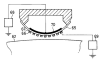
一方、図14に示す現像装置は、現像剤担持体202と、この現像剤担持体と圧接されトナー層を形成する層形成ブレード203と、現像剤担持体202と接触して、又は微小間隔をおいて支持される円筒状の帯電付与部材204と、現像剤担持体へトナーを供給するトナー供給部材205と、現像バイアス電源206と、トナー帯電用電源207とを備えている。そして、帯電付与部材204に電源207から電圧を印加して現像剤担持体202との間隙内で放電を発生させ、その放電現象で発生したイオン又は電子をトナーに付着させてトナーを帯電するものである。
【0007】
また、図15に示す現像装置は、現像剤担持体212と圧接するように層形成ブレード213を配設し、これに電源217からトナー帯電用の電圧を印加する。これにより層形成ブレード213と現像剤担持体212との間隙内で放電を発生させ、現像剤担持体212上にトナー層を形成するとともにトナーを帯電させるようにしたものである。
【0008】
上記のような図14又は図15に示す現像装置は、コロナ放電器ほどの高電圧を必要とせず、さらにオゾンの発生も少ないという利点がある。このような技術として、例えば特開昭54−17030号公報、特開昭62−291678号公報、特開昭64−62675号公報などに開示されている。
【0009】
【発明が解決しようとする課題】
しかしながら、上記図14又は図15に示す現像装置では以下に示すような問題点がある。
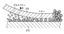
図14に示す現像装置では、帯電付与部材204に印加される電圧が放電電圧以下であると、体積抵抗率の高いトナーを使用しているため電荷誘導が十分に行われず、トナーを所望の極性に帯電することはできない。一方、印加電圧を上げることで電極からの放電現象によりトナーを帯電することが可能であるが、図16に示すように帯電付与部材204と現像剤担持体202との間には、放電に伴う電離により電子なだれ現象が発生しており、その結果、放電領域にプラスイオンと電子又はマイナスイオンという相反する極性のものが発生する。また、図15に示す現像装置でも同様に、層形成ブレード213と現像剤担持体212との間に電子なだれ現象が発生し、相反する極性のイオン等が発生する(図17)。
【0010】
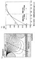
従って、トナーを所望の極性(本例ではマイナス)に帯電するため電子又はマイナスイオンのいずれかをトナーに付着させようとしても、放電領域は電離現象で発生したプラスイオンと電子又はマイナスイオンで満たされているため、電離域に満たされたプラスイオンと電子又はマイナスイオンの両方ともトナーに付与されてしまう。このため、放電により帯電されたトナーは所望の極性に揃わず、逆極性トナーが発生してしまう。これが、逆極性トナーが発生してしまうメカニズムであると考えられる。ここで逆極性は、本例のようにトナーをマイナスに帯電したい場合はプラス電荷をさすが、トナーをプラス帯電する場合はマイナス電荷が逆極性である。文献「放電現象」(東京電機大学出版、本多侃士著、64ページ)に基づいて、平行する2つの電極間に発生している電子とプラスイオンの相対密度を計算してみると、図18に示すように、プラスイオンは陽極(現像剤担持体)の極近傍にも存在し、トナーの大きさ(7μm〜10μm)において、電子の数千倍あることが示される。つまり、放電によりトナーをマイナスに帯電しようとした場合には、これと同時にかなりの量のプラスのトナーが発生すると考えられる。
【0011】
例えば、「最近の電子写真現像システムとトナー材料の開発・実用化」(日本科学情報株式会社出版部、竹内学。303ページ)の記載と同様に、トナー粒子1個1個の極性と帯電量を分布として計測する方法によれば、上記現像装置において発生する逆極性トナーは20wt%であった。このような逆極性のトナーが現像剤担持体の回転により現像領域に搬送されると、現像されたトナー像に地かぶりなどの画質劣化が発生し、良好な画像を得ることはできない。また、逆極性のトナーが現像剤担持体上から飛散し、機内のトナー汚染を招くという問題がある。
【0012】
本発明は、上記のような問題点に鑑みてなされたものであり、その目的は、逆極性のトナーの発生を防止して現像剤担持体上のトナーをほぼ均一に帯電し、長期にわたり良好な画質が得られる現像装置を提供することである。
【0013】
【課題を解決するための手段】
上記問題点を解決するために、請求項1に記載の発明に係る現像装置は、 表面に静電電位の差による潜像が形成された像担持体と近接もしくは接触するように配設される現像剤担持体と、 前記現像剤担持体の周面に現像剤の薄層を形成する層形成部材とを備え、 前記像担持体と前記現像剤担持体とが対向する現像領域で、薄層化された前記現像剤を前記像担持体に選択的に転移させて、前記潜像を可視化する現像装置において、 前記現像剤担持体上に既に現像剤の薄層が形成されている位置で該現像剤担持体と近接・対向するように配置され、前記現像剤担持体との間に電界を生じさせる電荷付与部材と、 該電荷付与部材と前記現像剤担持体との間に配置され、前記電荷付与部材と前記現像剤担持体とが直接に対向する部分が生じるように貫通部分が形成されて、前記電荷付与部材の電位と前記現像剤担持体の電位との間の電位が付与される帯電制御部材とを有し、 前記電荷付与部材と前記帯電制御部材との少なくとも一方は、半導電性材料からなるものであり、 前記帯電制御部材は、前記電荷付与部材に直接接触して、又は絶縁体層を介して接触配置され、 前記電荷付与部材と前記帯電制御部材の間に放電開始電圧以上の電圧を印加するとともに、該帯電制御部材と前記現像剤担持体との間には所定の極性のイオン又は電子が現像剤担持体側へ移動する電界を形成するように放電開始電圧以下の電圧を印加するものとする。
【0014】
かかる現像装置では、前記電荷付与部材に印加する電圧の平均値をVb(V)、前記帯電制御部材に印加する電圧の平均値をVm(V)としたときに、
|Vb|>|Vm|の条件を満たすように、電荷付与部材と帯電制御部材に独立の電圧を印加するものとし、電荷付与部材と帯電制御部材との間に放電開始電圧以上の電圧を印加するとともに、電荷付与部材と現像剤担持体との間には帯電したい極性のイオン又は電子が現像剤担持体側へ移動するように電界を形成するが、放電を生じないように電圧を設定する。
【0015】
このような現像装置では、電荷付与部材と帯電制御部材との間に放電開始電圧以上の電圧を印加することで強い電界が形成され、両者間で放電が発生する。この放電により電離現象が発生し、電子なだれ現象によりプラスイオンと電子およびマイナスイオンが発生するが、電離域は電荷付与部材と帯電制御部材との間に限定され、帯電制御部材と現像剤担持体との間、すなわち現像剤担持体上に薄層形成されたトナーの存在している領域では電離は生じない。このため、トナー層の厚さの範囲内での電離は発生せず、プラスイオンとマイナスイオンとが生成されない。
【0016】
一方、帯電制御部材と現像剤担持体との間には放電を開始するよりも小さい電界が形成されており、帯電制御部材と現像剤担持体との間の電界作用によって、電荷付与部材と帯電制御部材との間とその近傍に発生したプラスイオン又はマイナスイオン等のいずれか一方が現像剤担持体側に引き付けられ、現像剤担持体上に形成されたトナー層に付与される。これにより、トナーを所望の極性に帯電することが可能となる。
【0017】
このような現像装置において、電荷付与部材と帯電制御部材とはいずれも導電性材料又は半導電性材料からなるものとすることができるが、持続的な放電を生じさせるために、いずれか一方は半導電性材料からなるものとするのが望ましい。ここで、半導電性材料とは体積抵抗が103 Ω・cm〜1011Ω・cm程度のものである。
帯電制御部材の形状はトナーをほぼ均一に帯電させることができるものであれば適宜に設定することが可能であり、例えば請求項2に記載の発明のように、導電性材料又は半導電性材料からなる網状部材や、請求項3に記載の発明のように、多数の小孔を有する導電性又は半導電性の薄板部材とすることができる。この帯電制御部材は電荷付与部材と微小間隙をおいて支持されてもよいし、一部が接触するように支持されるものでもよい。また、この電荷付与部材と帯電制御部材との間に、絶縁材料からなり、多数の小さな開口を有する薄い網状部材又は板状部材を介挿してもよい。
【0018】
請求項4に記載の発明は、 表面に静電電位の差による潜像が形成された像担持体と近接もしくは接触するように配設される現像剤担持体と、 前記現像剤担持体の周面に現像剤の薄層を形成する層形成部材とを備え、 前記像担持体と前記現像剤担持体とが対向する現像領域で、薄層化された前記現像剤を前記像担持体に選択的に転移させて、前記潜像を可視化する現像装置において、 前記現像剤担持体上に既に現像剤の薄層が形成されている位置で該現像剤担持体と近接・対向するように配置され、前記現像剤担持体との間に電界を生じさせる電荷付与部材と、 該電荷付与部材と前記現像剤担持体との間に配置され、前記電荷付与部材と前記現像剤担持体とが直接に対向する部分が生じるように貫通部分が形成されて、前記電荷付与部材の電位と前記現像剤担持体の電位との間の電位が付与される帯電制御部材とを有し、 前記電荷付与部材は、円筒状に形成され、軸線回りに回転可能に支持されており、 前記帯電制御部材は、前記電荷付与部材より径が大きい円筒状に形成され、該電荷付与部材に外挿されて、前記現像剤担持体との対向位置で内周面の一部が該電荷付与部材と接触して回転するように支持され、 前記電荷付与部材と前記帯電制御部材の間に放電開始電圧以上の電圧を印加するとともに、該帯電制御部材と前記現像剤担持体との間には所定の極性のイオン又は電子が現像剤担持体側へ移動する電界を形成するように放電開始電圧以下の電圧を印加するものとする。
【0019】
このような現像装置では、電荷付与部材、帯電制御部材及び現像剤担持体が共に回転し、電荷付与部材と帯電制御部材との接触部近傍の微小間隙で放電が発生する。そして、この放電は電荷付与部材の現像剤担持体と対向する部分に限定されるので、電荷付与部材と帯電制御部材との間で過大な電流が流れるのを防止することができる。
【0020】
また、この現像装置では、請求項5に記載の発明のように、前記帯電制御部材が、前記電荷付与部材と前記現像剤担持体とに挟持され、前記現像剤担持体の回転に従動して回転駆動されるものとすることができる。これにより、帯電制御部材の支持構造が簡単になり、装置の大型化や複雑化を防止できる。
【0021】
また、請求項6に記載の発明のように、前記帯電制御部材が、前記現像剤担持体と離隔するように支持され、周速度が前記現像剤担持体の周速度と差を有するように回転駆動されるものとすることもできる。これにより、帯電制御部材の電極部又は開口部とは現像剤担持体の表面と相対的に移動し、現像剤担持体上の現像剤をより均一に帯電することが可能となる。
【0022】
請求項7に記載の発明に係る現像装置では、前記帯電制御部材が、前記電荷付与部材の表面上に絶縁性層を介して積層された導電性層又は半導電性層によって形成されている。これにより、電荷付与部材と帯電制御部材と間でのリーク現象が防止され、安定した放電によりトナーを良好に帯電させることができる。また、帯電制御部材と帯電付与部材とを一体とすることで、装置の大型化や複雑化を防止できる。ここで、上記絶縁性層は体積抵抗が1012Ω・cm程度以上の材料で形成された層である。
【0023】
また、この現像装置では、請求項8に記載の発明のように、前記電荷付与部材が、前記層形成部材と一体となるように支持されるものとすることができる。これにより、層形成部材によって現像剤担持体上に現像剤層が形成されるとともに、電荷付与部材の近傍で放電を発生させることができる。このため、現像剤層の形成とともに現像剤を帯電させることが可能となり、装置の大型化や複雑化を防止できる。
【0024】
請求項9に記載の発明は、 表面に静電電位の差による潜像が形成された像担持体と近接もしくは接触するように配設される現像剤担持体と、 前記現像剤担持体の周面に現像剤の薄層を形成する層形成部材とを備え、 前記像担持体と前記現像剤担持体とが対向する現像領域で、薄層化された前記現像剤を前記像担持体に選択的に転移させて、前記潜像を可視化する現像装置において、 前記現像剤担持体上に既に現像剤の薄層が形成されている位置で該現像剤担持体と近接・対向するように配置され、前記現像剤担持体との間に電界を生じさせる電荷付与部材と、 該電荷付与部材と前記現像剤担持体との間に配置され、前記電荷付与部材と前記現像剤担持体とが直接に対向する部分が生じるように貫通部分が形成されて、前記電荷付与部材の電位と前記現像剤担持体の電位との間の電位が付与される帯電制御部材とを有し、 前記帯電制御部材は、前記電荷付与部材の表面上に絶縁性層を介して積層された導電性層又は半導電性層によって形成されており、 前記電荷付与部材が、回転可能な円筒状部材又は周回可能な無端ベルト状部材からなり、該電荷付与部材の周速度が、前記現像剤担持体の周速度と差を生じるように駆動されるものであり、 前記電荷付与部材と前記帯電制御部材の間に放電開始電圧以上の電圧を印加するとともに、該帯電制御部材と前記現像剤担持体との間には所定の極性のイオン又は電子が現像剤担持体側へ移動する電界を形成するように放電開始電圧以下の電圧を印加するものとする。
このような装置では、帯電制御部材である電極層と現像剤担持体の表面が相対的に移動し、放電は微視的には均一に生じてはいないが、現像剤担持体上の現像剤をより均一に帯電することが可能となる。
【0025】
また、請求項10に記載の発明に係る現像装置では、前記帯電制御部材の少なくとも一部が半導電性材料又は絶縁性材料で被覆されているものとすることができる。これにより、電荷付与部材と帯電制御部材との間又は帯電制御部材と現像剤担持体との間でリーク現象や電荷付与部材表面の電位低下による帯電性不良が発生するのが防止され、トナーを良好に帯電させることができる。
【0026】
なお、上記現像装置では、電荷付与部材と被帯電体である現像剤担持体との間に帯電制御部材を配置することで、イオン等を発生する電離領域を帯電付与部材側に制限するものであるが、従来帯電器として使われるスコロトロン帯電器も、本発明と似た構成を取る。すなわち、スコロトロン帯電器では、放電ワイヤーは本発明の帯電付与部材であり、被帯電体は感光体や現像剤担持体であり、また本発明の帯電制御部材は放電ワイヤーと被帯電体との間に配設されるスクリーングリッド電極に相当すると考えることもできる。しかしながら、スコロトロン帯電器では、放電ワイヤーの直径が30〜100μmと小さいため、帯電制御部材がなくても、放電ワイヤーがそれを囲むシールド電極及び被帯電体との間で発生させる電界はワイヤー近傍のみで電離を引き起こし、シールドと被帯電体の近傍ではイオン又は電子が移動するのみである。つまり、スクリーングリッド電極は、帯電しようとする極性のイオン又は電子の移動を制限して被帯電体の帯電電位が一定になる働きをしており、放電による電離領域を制御する働きは積極的にはない。これに対して本願発明は、2つの微小な電極間における電界を電離領域と電子やイオンの移動領域とに分離する働きを有しており、被帯電体付近で帯電しようとする極性と逆極性のイオンが多量に発生するのを制限するもので、機能が従来のスコロトロン帯電器と全く異なっている。
【0027】
【発明の実施の形態】
以下、本発明の実施の形態を図に基づいて説明する。
図1は、請求項1、請求項2、請求項4又は請求項5に記載の発明の一実施形態である現像装置を示す概略構成図である。
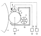
この現像装置は、表面に帯電電位の差による潜像を形成することができる像担持体1との対向位置に設けられており、ハウジング10内に、像担持体1と近接対向し表面にトナーを付着して搬送する現像剤担持体2と、この現像剤担持体上のトナーを規制してトナー層を形成する層形成部材3と、トナーを撹拌するとともに現像剤担持体2にトナーを供給する撹拌供給部材4と、現像剤担持体2と対向して配置され、この対向位置に放電を生じさせる電荷付与部材5と、この電荷付与部材5と現像剤担持体2との間に配置され、これらの間に生じる放電の電離領域を制限する帯電制御部材6とを備えている。さらに、現像剤担持体2と像担持体1との間に現像用の電圧を印加する現像用電源7と、現像剤担持体2と電荷付与部材5との間にトナー帯電用の電圧を印加するトナー帯電用電源8と、帯電制御部材6に電離領域を制限するための電圧を印加する帯電制御用電源9とを備えている。
【0028】
上記現像剤担持体2は、回転可能に支持され、現像用電源7からトナーと同極性の約−200Vの直流電圧が印加されるものである。これにより、現像剤担持体2と像担持体1との間に電界が形成され、トナーが像担持体1上の潜像に転移されるようになっている。この現像剤担持体は、アルミニウムやステンレスの丸棒やパイプを切削加工した後、外周面にサンドブラスト、液体ホーニング、エメリー研磨等の機械加工を施すか、或いは化学腐食を施すことによりRa=0.1〜5.0μm程度の凹凸を形成したものである。また、アルミニウムやステンレスの丸棒やパイプを切削加工した後に、導電粉を分散させた樹脂層を形成したものでもよい。本例の現像剤担持体2はΦ20mmとなっており、アルミニウムのパイプを切削加工した後、外周面にサンドブラスト陽極酸化処理を施したものが用いられている。また、現像用電源7から印加される電圧は、現像性能を確保するため直流電圧と交流電圧とを重畳した電圧としてもよい。
【0029】
上記層形成部材3は、厚さ0.03〜0.3mm程度のステンレスの板バネに、導電性粉を分散させたSiゴムやEPDMゴムからなる圧接部材を加硫接着したものであり、現像剤担持体2への接触圧力は5〜100g/cm程度に設定されている。また、ゴムの硬度は20〜80度のものが使用可能であり、好ましくは30〜60度が適している。このような層形成部材3で圧接されることにより、現像剤担持体2上に5〜30μm程度のトナー層が形成されるようになっている。
【0030】
上記電荷付与部材5は、円筒状に形成され、軸線回りに回転可能に支持されている。この電荷付与部材5は、イオン導電体を含んだもの、もしくはゴムに導電性微粒子を配合したものであり、体積抵抗率が105 〜1010Ω・cm程度のものである。この体積抵抗率は、特に107 〜108 Ω・cm程度が望ましい。
【0031】
上記帯電制御部材6は、線径50μm、ピッチ127μmのステンレスのメッシュ状部材からなり、電荷付与部材5より径が大きい円筒状に形成されている。この帯電制御部材6は、電荷付与部材5に外挿され、該電荷付与部材5と現像剤担持体2とに挟持されており、現像剤担持体2との対向位置で内周面の一部が電荷付与部材5と接触して回転するようになっている。このとき、帯電制御部材6は現像剤担持体2の回転に従動して回転駆動される。
【0032】
また、現像剤担持体2上のトナーを負極性に帯電するためには、電荷付与部材5と帯電制御部材6との間には放電を開始するように電界を形成し、帯電制御部材6と現像剤担持体2との間には放電を生じない程度に勾配の小さい電界であって、負電荷を現像剤担持体側に引き付ける方向の電界を形成する。このため、帯電制御部材6と現像剤担持体2との電位の関係は、例えば以下の関係に保たれている。
(現像剤担持体電位)−(帯電制御部材電位)=100V
【0033】
また、帯電付与部材5と帯電制御部材6との電位の関係は、以下の関係に保たれている。
(帯電制御部材電位)−(電荷付与部材電位)=1000V
なお、これらの部材の電位は電荷付与部材5と現像剤担持体2との間隔、帯電制御部材6の構造・厚さ等によって適宜決定されるものである。また、電荷付与部材5、帯電制御部材6、および現像剤担持体2が、それぞれ間隙をおいて設けられるときにはこれらの間隙の大きさも考慮して定められる。本例では、現像剤担持体2には電源7から−200Vの電圧が印加され、帯電制御部材6には電源9から−300Vの電圧が印加され、電荷付与部材5のシャフトには電源8から−1300Vの電圧が印加されている。
【0034】
なお、上記現像装置で用いられる現像剤は一成分系のトナーであり、スチレン樹脂、アクリル樹脂若しくはポリエステル樹脂等の各種熱可塑性樹脂中に顔料や含金属アゾ染料等の極性制御剤を分散し、粉砕、分級により3〜20μm(平均粒径7μm)の大きさにしたものである。また電荷制御剤が添加され、負極性の電荷が付与されている。電荷制御剤としては、疎水化処理したシリカ、アルミナ、チタン等の0.1μm以下の微粒子が用いられるが、疎水性シリカが最も望ましい。またトナーの流動性助剤が外添されている。
なお、上記像担持体1としてはセレン系感光体や有機感光体が用いられ、像担持体1と現像剤担持体2とは接触してもよいし、あるいは100μm〜400μm程度の間隙をおいて対向させてもよい。
【0035】
このような現像装置では、撹拌供給部材4の回転によりハウジング10内のトナーが撹拌され、現像剤担持体2に供給される。現像剤担持体2の表面付近のトナーは現像剤担持体2の回転により層形成部材3との対向位置へ搬送され、層形成部材3の押圧力により現像剤担持体2上にトナー層が形成される。その後、トナー層は電荷付与部材5及び帯電制御部材6との対向位置に搬送される。このとき、電荷付与部材5と帯電制御部材6との間、及び帯電制御部材6と現像剤担持体2との間には上記のような電圧が印加されており、これらが対向する領域に電界が形成される。このとき、現像剤担持体上のトナーが帯電される状態を図2及び図3を用いて説明する。
【0036】
電荷付与部材5と現像剤担持体2との間に電制御部材6が入らないときの電位分布はこの間隙内でほぼ均一な電界となるが、帯電制御部材6が間に入り、これに電圧が印加されることにより、図3(a)に示すように電界が歪み、不均一な電界となる。図3(b)は、図3(a)中の直線A−A′に沿った電位変化を示したものであり、これにPaschenの放電開始電界の勾配Bを重ねると、接点Cより電界が大きい電荷付与部材5の側のみが放電可能であり、現像剤担持体2の側の電界は放電開始電界より小さいため電離しない。従って、図2に示すように電荷付与部材5の付近では放電に伴う電離によりマイナスイオン又は電子の他にプラスイオンが発生するが、現像剤担持体2の近傍では電離が発生せず、帯電制御部材6と現像剤担持体2との間の電界作用によりマイナスイオン又は電子が現像剤担持体に引き付けられる。そして、この電荷が現像剤担持体上のトナーに付着し、トナーが帯電される。従って、電離にともなって発生するプラスイオンは電荷付与部材5の側でのみ存在し、電荷付与部材5へ吸着されるが、現像剤担持体2上のトナーに付着することはない。このように、電荷付与部材5と現像剤担持体2との間にメッシュ状の帯電制御部材6を配置することにより、電離領域がトナーから離れた場所に限定されるので、逆極性トナーの発生が抑制される。
【0037】
このようにして均一な電荷が付与されたトナー層は、現像剤担持体2の回転により像担持体1と対向する現像領域に搬送される。そして、現像剤担持体2と像担持体1との間に形成される現像電界により、上記トナーが像担持体1の潜像に転移して現像が行われる。
【0038】
このような現像装置において、トナーの帯電効果を確認したところ、トナーは−7μC/gから−12μC/gに帯電され、逆極性のトナーは0.1wt%以下であり、良好な帯電性が得られた。
【0039】
なお、上記現像装置では、帯電制御部材が回転するのに伴って軸方向に移動することがあるため、電荷付与部材の中央部分の径を太くしてもよい。また、現像剤担持体と逆方向にテンションロール部材を設け、そのロールの軸方向における中央部分の径を太くしてもよい。
【0040】
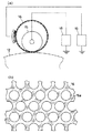
図4は、請求項1、請求項4又は請求項5に記載の発明の一実施形態である現像装置の帯電制御部材付近の構成を示す拡大図である。
この現像装置は、上記図1に示す現像装置とほぼ同じ構成であるが、図4(b)に示すように、帯電制御部材16がフォトエッチング、エレクトロフォーミング、レーザー加工などにより作成した、多数の円形小孔16aを有する導電性フィルムからなる。この帯電制御部材16は、現像剤担持体12と接触し、現像剤担持体2の駆動により帯電制御部材16が従動回転するとともに、この帯電制御部材16の回転により電荷付与部材15が回転するようになっている。
なお、この現像装置の他の構成は上記図1に示す現像装置と同じである。
【0041】
このような現像装置では、電荷付与部材15と帯電制御部材16との間の電界により放電現象が生じ、プラスイオンとマイナスイオン又は電子が発生するとともに、帯電制御部材16と現像剤担持体12との間の電界によりマイナスイオン又は電子が現像剤担持体12上に引き付けられる。これにより、現像剤担持体2上のトナーに負極性の電荷が与えられ、トナーが均一に帯電される。
【0042】
上記現像装置では、帯電制御部材16が円筒形状であるため連続的に回転が可能であり、現像剤を効率的に帯電することが可能である。また帯電制御部材16が電荷付与部材15の一部にのみ接触しているため、現像剤に近接していない部分すなわち現像剤の帯電に寄与されない部分での放電は発生せず、装置全体としての放電量が少なくなる。このため、必要な電流が少なくて済み、電源の小型化及び低コスト化が可能である。また、放電量が少ないため放電生成物、例えばオゾンなどの発生量を抑えることができる。また、現像剤の帯電に必要な放電現象は、電荷付与部材15と帯電制御部材16との接触もしくは近接部分により十分に確保されるため、現像剤の帯電能力が損なわれることはない。
【0043】
このような現像装置において、帯電制御部材16に印加する電圧を−300V、電荷付与部材15に印加する電圧を−1300V、及び現像剤担持体12に印加する電圧を−200Vに設定してトナーの帯電テストを行ったところ、逆極性のトナーは0.1wt%以下であり、良好な帯電性が得られることが確認された。
【0044】
図5は、請求項1、請求項4又は請求項6に記載の発明の一実施形態である現像装置の帯電制御部材付近の構成を示す拡大図である。
この現像装置では、図5(a)に示すように、電荷付与部材25は円筒状の半導電性部材であるが、両端部に設けられたトラッキングロール27により現像剤担持体22と微小間隙をおいて支持されている。帯電制御部材26は、図5(b)に示すように、多数の長円状の小孔26aを長手方向に配列した導電性フィルムからなり、電荷付与部材25より径が太い円筒状に形成され、この電荷付与部材25に外挿されている。また、この帯電制御部材26は、現像剤担持体22と接触しないように、両端部でバネ部材により現像剤担持体22とは逆方向に付勢されている。したがって、帯電制御部材26は内周面の一部が電荷付与部材25と接触しており、電荷付与部材25の回転に従動して帯電制御部材26が回転するようになっている。このとき、帯電制御部材26の周速度が現像剤担持体22の周速度と差を有するように回転駆動される。
なお、この現像装置の他の構成は上記図1に示す現像装置と同じである。
【0045】
このような現像装置では、帯電制御部材26が現像剤担持体と離隔して回転可能であり、周速差によって現像剤担持体22の表面と相対的に移動し、帯電制御部材26の開口の形状による帯電むらの発生を低減することができる。さらに、帯電制御部材26の周速度が現像剤担持体22の周速度と差を有するように回転駆動されているので、帯電制御部材26の電極部分と小孔との両箇所が現像剤担持体22の表面と対向することになり、現像剤をほぼ均一に帯電することができる。
【0046】
図6は、本願発明に係る現像装置とほぼ同じ効果が得られる他の現像装置の帯電制御部材付近の構成を参考に示す拡大図である。
この現像装置は、帯電制御部材36が多数の小孔を有する導電性の薄板部材からなり、電荷付与部材35は帯電制御部材36とほぼ同じ面積を有する板状の電極からなる。この帯電制御部材36は、両端部に設けられたトラッキング部材37により電荷付与部材35と微小間隔をおいて離隔されるとともに、現像剤担持体32と近接・対向するように支持されている。
また、上記現像装置では、帯電制御部材36の小孔が直径約80μmで、電極部分となる小孔間の最小幅は約30μmに形成されており、電荷付与部材35が現像剤担持体32に対向しても現像剤担持体付近で放電が発生しないような電圧が印加される設定となっている。
なお、この現像装置の他の構成は上記図1に示す現像装置と同じである。
【0047】
このような現像装置では、電荷付与部材35と帯電制御部材36との微小間隙で放電を発生させることができ、この放電現象により発生した電子又はマイナスイオンのみが現像剤担持体32上のトナーに付与され、トナーが帯電される。このような現像装置では、電荷付与部材35と帯電制御部材36との支持構造が簡単であるので、装置全体の小型化及びコストの低減が可能となる。
なお、本例では、帯電制御部材36と電荷付与部材35との間隙をトラッキング部材37により保持しているが、現像装置に設けられた位置決め部材に取り付けるような構成としてもよい。
【0048】
図7は、請求項1又は請求項7に記載の発明の第1の実施形態である現像装置の帯電制御部材付近の構成を示す拡大図である。
この現像装置では、電荷付与部材45が図7(a)に示すような円筒状の部材であり、周面に半導電性フィルム層45aが形成されている。帯電制御部材46は、図7(b)に示すように、半導電性フィルム層45aの表面上に絶縁性層47を介して積層された導電性層によって形成されている。この帯電制御部材46は、図7(c)に示すような多数の円形小孔46aを有する導電性層を、無電界めっきやレーザ加工などの方法により形成したものであり、この導電性層に電源49から約−300Vの電圧が印加されるようなっている。また、半導電性フィルム層45aの背面側には給電部材45bが配設されており、この給電部材45bを介して電源49から約−1300Vの電圧が印加されるようになっている。上記帯電制御部材46は、上記のように円形小孔を有するものに限らず、ストライプ状に導電性層を形成したもの等、様々な態様のものとすることができる。
なお、この現像装置の他の構成は上記図1に示す現像装置と同じである。
【0049】
このような現像装置では、半導電性フィルム層を有する電荷付与部材45と、絶縁層47を介して積層された帯電制御部材46との間に放電が発生し、電離現象により電子又はマイナスイオンとプラスイオンとが発生する。このうち電子又はマイナスイオンのみが現像剤担持体42との間に生じる電界により引き付けられ、現像剤担持体上のトナーに付与される。
このような現像装置では、電荷付与部材45と帯電制御部材46との間に絶縁性層が介在されているので、両者間のリーク現象、電荷付与部材45の表面電位の低下、および両者間で過大な電流が流れるのを防止することができる。また、両者間での放電領域を拡大することが可能となり、現像剤の帯電効率を向上することができる。
【0050】
このような現像装置において帯電テストを行ったところ、逆極性トナーは0.1wt%以下となり、良好な帯電性が得られることが確認された。また、電荷付与部材45と帯電制御部材46とが一体の部材として形成されているので、装置の簡略化や低コスト化を図ることができる。なお、上記現像装置において、電荷付与部材45が有する半導電性フィルム層45aは、半導電性のゴム層であってもよい。
【0051】
図8は、請求項1又は請求項7に記載の発明の第2の実施形態である現像装置の帯電制御部材付近の構成を示す拡大図である。
この現像装置は、電荷付与部材55が半導電性フィルムで形成されており、一方の端部が固定され、もう一方が現像剤担持体52の表面と当接するように支持されている。また、帯電制御部材56は、図7に示す構成と同様に電荷付与部材55の表面上に絶縁性層57を介して積層されており、現像剤担持体52と近接して対向する位置に形成されている。さらに、電荷付与部材55の背面側には、該電荷付与部材55に電圧を印加する給電部材60が設けられている。
なお、この現像装置の他の構成は上記図1に示す現像装置と同じである。
【0052】
このような現像装置では、電荷付与部材55と帯電制御部材56との間に放電現象により電離が発生するが、帯電制御部材56と現像剤担持体32との間の電界の作用により電子又はマイナスイオンのみが現像剤担持体52に引き付けられる。このため、現像剤担持体上のトナーをほぼ均一に帯電することができる。また、電荷付与部材55と帯電制御部材56とが一体の部材として形成されるので、装置の簡略化や低コスト化を図ることができる。
【0053】
図9は、請求項1又は請求項7に記載の発明の第3の実施形態である現像装置の帯電制御部材付近の構成を示す拡大図である。
この現像装置は、電荷付与部材65が半導電性フィルムで形成されており、その両端部が固定支持されている。また、帯電制御部材66は、電荷付与部材65の表面上に絶縁性層67を介して積層されており、該帯電制御部材66が現像剤担持体62と微小間隔をおいて離隔するように支持されている。また、電荷付与部材65の背面側には給電部材70が設けられている。
なお、この現像装置の他の構成は上記図1に示す現像装置と同じである。
【0054】
このような現像装置でも上記と同様に、現像剤担持体上のトナーをほぼ均一に帯電することができる。さらに、電荷付与部材65及び帯電制御部材66の構成及び支持構造が簡単であり、装置の小型化や低コスト化を図ることができる。
【0055】
図10は、請求項1、請求項7又は請求項9に記載の発明の一実施形態である現像装置の帯電制御部材付近の構成を示す拡大図である。
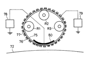
この現像装置では、電荷付与部材75が可撓性を有する半導電性フィルムからなり、円筒形状に形成されている。この電荷付与部材75の周面上には絶縁性層77を介して積層された導電性層からなる帯電制御部材76を備えている。また、電荷付与部材75の内周面側には現像剤担持体72と対向する位置に給電部材80が配設されており、電荷付与部材と当接して所定の電位を付与するようになっている。さらに、この電荷付与部材75の内面と当接するように3つの支持ローラR1 ,R2 ,R3 が配設され、これらによって周回可能に支持されている。そして、電荷付与部材75の周速度が現像剤担持体72の周速度と差を生じるように駆動される。
なお、この現像装置の他の構成は上記図1に示す現像装置と同じである。
【0056】
このような現像装置では、電荷付与部材75が周回可能に支持されているので、帯電制御部材76の形状による帯電むらがなくなり、現像剤を好適な電位に帯電することが可能となる。また、電荷付与部材75の周速度が現像剤担持体72の周速度と差を生じるように駆動されているので、帯電制御部材76の電極部又は非電極部と対向する現像剤担持体表面の位置が移動し、現像剤をほぼ均一に帯電することができる。
【0057】
また、上記現像装置では、帯電制御部材76と現像剤担持体72とを非接触に支持しているが、両者が接触するように支持してもよい。このとき、電荷付与部材75が可撓性を有するため、現像剤担持体と接触した際に現像剤に与える機械的ストレスを低減することが可能となる。また、現像剤担持体72と接触させた際には、帯電制御部材の表面にトナーの粒径以下の微小開口部を有する保護膜を設けるとよい。この保護膜は離型性のよい材料で形成されていることが好ましく、例えばフッ素樹脂などを用いることができる。これにより、トナーが帯電制御部材に付着するのを防止することができ、より均一な帯電が得られる。
【0058】
図11は、請求項1、請求項7又は請求項8に記載の発明の第1の実施形態である現像装置を示す概略構成図である。
この現像装置では、現像剤担持体82上にトナー層を形成する層形成部材83と電荷付与部材85とが一体となるように支持されたものであり、層形成部材83の表面に給電部材90が装着され、この給電部材90上に電荷付与部材85が設けられている。また、電荷付与部材85の表面には絶縁性層87が形成されており、この絶縁性層を介して導電性の帯電制御部材86が積層されている。
【0059】
上記層形成部材83は板状の保持部材83aとこれに接着された弾性部材83bとを有し、層形成部材83が現像剤担持体82に圧接されるように支持されている。層形成部材83の先端部は現像剤担持体82の回転方向に対して上流側に向けて配置されており、現像剤担持体82上のトナーが層形成部材83との圧接部を通過することによりトナー量が規制されるようになっている。
また、上記電荷付与部材85及び帯電制御部材86は、弾性部材83b表面の現像剤担持体82との接触部より支持端側に形成されており、帯電制御部材86が現像剤担持体82と離隔して対向するように設けられている。
なお、この現像装置の他の構成は上記図1に示す現像装置と同じである。
【0060】
このような現像装置では、現像剤担持体82の回転によりトナーが層形成部材83との圧接部を通過し、現像剤担持体82上にトナー層が形成される。そして、このトナー層は帯電制御部材86との対向位置を通過し、電荷付与部材85と帯電制御部材86との間の放電現象により発生したマイナスイオン及びプラスイオン等のうち、電子又はマイナスイオンのみが現像剤担持体82との間に生じる電界によりトナーに付与される。
【0061】
このような現像装置を用いてトナーの帯電性能を確認したところ、逆極性トナーは0.1wt%以下となり、良好な結果が得られた。また、電荷付与部材85と層形成部材83とが一体として支持されているので、装置の小型化や低コスト化を図ることができる。
【0062】
図12は、請求項1、請求項7又は請求項8に記載の発明の第2の実施形態である現像装置の帯電制御部材付近の構成を示す拡大図である。
この現像装置では、給電部材が層形成部材93の保持部材93aを兼ねており、弾性部材93bに並列して半導電性材料からなる電荷付与部材95が形成されている。また、この電荷付与部材95の表面上には絶縁性層97が形成されており、この絶縁性層を介して導電性の帯電制御部材96が積層されている。この帯電制御部材96は、現像剤担持体92と離隔して対向するように設けられている。
なお、この現像装置の他の構成は上記図1に示す現像装置と同じである。
【0063】
このような現像装置では、層形成部材93により現像剤担持体92上にトナー層が形成されるとともに、このトナー層は帯電制御部材96との対向位置を通過する。このとき、電荷付与部材95と帯電制御部材96との間の放電現象により発生したマイナスイオン及びプラスイオン等のうち、電子又はマイナスイオンのみが現像剤担持体92との間に生じる電界によりトナーに付与される。このため、トナーをほぼ均一に帯電することができる。
【0064】
図13は、請求項1、請求項7又は請求項8に記載の発明の第3の実施形態である現像装置の帯電制御部材付近の構成を示す拡大図である。
この現像装置は、導電性の保持部材103の先端部に、板状の半導電性材料からなる電荷付与部材105が装着されており、これがトナー層形成部材を兼ねている。この電荷付与部材105の表面上には絶縁性層107を介して導電性の帯電制御部材106が積層されている。また、帯電制御部材106の表面にはトナーの粒径以下の微小開口部を有する保護膜101が形成されている。この保護膜には例えばフッ素樹脂などが用いられる。
なお、この現像装置の他の構成は上記図1に示す現像装置と同じである。
【0065】
この現像装置では、電荷付与部材105が現像剤担持体102に圧接されることにより現像剤担持体102上にトナー層が形成されるとともに、このトナー層に、電荷付与部材105と帯電制御部材106との間の放電現象により発生したイオン等のうち、電子又はマイナスイオンのみが付与される。このため、トナーをほぼ均一な極性に帯電することができる。また、帯電制御部材106の表面には保護膜101が形成されているので、トナーが帯電制御部材に付着するのを防止することができ、より均一な帯電が得られる。
【0066】
なお、以上に説明した実施形態の現像装置において、導電性の帯電制御部材が電荷付与部材又は現像剤担持体と直接に接触する場合には、帯電付与部材の表面に絶縁性材の被覆層を設けてもよい。この被覆層によって電荷付与部材の電位の変動や電荷のリーク現象を低減することができ、トナーをより均一に帯電することができる。
【0067】
【実施例】
本願発明に係る現像装置のトナー帯電性能を確認するために、下記の条件にて長時間のプリントテストを行った結果について説明する。この実験では、現像装置は図4と同じ構成のものが用いられている。

上記条件にてプリントテストを行ったところ、従来問題であった、地かぶりや、逆極性トナーによる機内へのトナー飛散の発生はなく、維持性に優れていることが確認された。
【0069】
【発明の効果】
以上説明したように、請求項1に記載の発明に係る現像装置では、電荷付与部材と帯電制御部材との間の放電現象によりプラスイオンとマイナスイオン等の両方が発生するが、帯電制御部材と現像剤担持体との間では電子なだれ現象は起こらず、電界の作用によってプラスイオン又はマイナスイオン等のいずれか一方が現像剤担持体側に引き付けられて現像剤担持体上のトナーをほぼ均一に帯電することが可能となる。
【0070】
また、請求項2又は請求項3に記載の現像装置では、帯電制御部材の形状が適切に設定されているので、帯電制御部材の形状に起因する帯電むらの発生を極力抑えることができる。
【0071】
また、請求項4に記載の発明に係る現像装置では、電荷付与部材、帯電制御部材及び現像剤担持体が共に回転し、電荷付与部材と帯電制御部材との接触部近傍の微小間隙で放電が発生するので、各部材間に過大な電流が流れたり、リーク現象が発生するのを抑制することができ、現像剤担持体上の現像剤を好適に帯電することができる。
【0072】
また、請求項5に記載の発明に係る現像装置では、帯電制御部材が電荷付与部材と現像剤担持体とに挟持され、現像剤担持体の回転に従動して回転駆動されるので、帯電制御部材の支持構造が簡単になり、装置の大型化や複雑化を防止できる。
【0073】
請求項6に記載の発明に係る現像装置では、帯電制御部材の電極部又は非電極部が現像剤担持体の表面に対して移動するようになっているので、現像剤担持体上の現像剤をより均一に帯電することができる。
【0074】
請求項7に記載の発明に係る現像装置では、電荷付与部材と帯電制御部材との間に絶縁性層が介在されているので、両者間でのリーク現象が防止され、トナーを均一かつ良好に帯電させることができる。また、帯電制御部材と帯電付与部材とを一体とすることで、装置の大型化や複雑化を防止することができる。
【0075】
請求項8に記載の発明に係る現像装置では、電荷付与部材が層形成部材と一体となるように支持されているので、現像剤担持体上の現像剤層の形成とともに現像剤を帯電させることが可能となり、装置を簡略化することができる。
【0076】
請求項9に記載の発明に係る現像装置では、帯電制御部材の電極層又は該電極層が形成されていない部分とが現像剤担持体の表面と対向し、相対的に移動するので、現像剤担持体上の現像剤をより均一に帯電することができる。
【0077】
請求項10に記載の発明に係る現像装置では、電荷付与部材の少なくとも一部が半導電性材料又は絶縁性材料で被覆されているので、電荷付与部材と帯電制御部材との間、もしくは帯電制御部材と現像剤担持体との間でのリーク現象が防止され、トナーを良好に帯電させることができる。
【図面の簡単な説明】
【図1】請求項1、請求項2、請求項4又は請求項5に記載の発明の一実施形態である現像装置を示す概略構成図である。
【図2】上記現像装置において、現像剤担持体上の現像剤が帯電されるメカニズムを示す図である。
【図3】上記現像装置の電荷付与部材と現像剤担持体との間の電位分布を示す図である。
【図4】請求項1、請求項4又は請求項5に記載の発明の他の実施形態である現像装置の電荷付与部材および帯電制御部材を示す部分構成図である。
【図5】請求項1、請求項4又は請求項6に記載の発明の一実施形態である現像装置の電荷付与部材および帯電制御部材を示す部分構成図である。
【図6】請求項1又は請求項3に記載の発明の一実施形態である現像装置の電荷付与部材および帯電制御部材を示す部分構成図である。
【図7】請求項1又は請求項7に記載の発明の第1の実施形態である現像装置の帯電制御部材を示す概略構成図である。
【図8】請求項1又は請求項7に記載の発明の第2の実施形態である現像装置の電荷付与部材および帯電制御部材を示す部分構成図である。
【図9】請求項1又は請求項7に記載の発明の第3の実施形態である現像装置の電荷付与部材および帯電制御部材を示す部分構成図である。
【図10】請求項1、請求項7又は請求項9に記載の発明の一実施形態である現像装置の電荷付与部材および帯電制御部材を示す部分構成図である。
【図11】請求項1、請求項7又は請求項8に記載の発明の第1の実施形態である現像装置を示す概略構成図である。
【図12】請求項1、請求項7又は請求項8に記載の発明の第2の実施形態である現像装置の電荷付与部材および帯電制御部材を示す部分構成図である。
【図13】請求項1、請求項7、請求項8に記載の発明の第3の実施形態である現像装置の電荷付与部材および帯電制御部材を示す部分構成図である。
【図14】従来の現像装置の一例を示す概略構成図である。
【図15】従来の現像装置の他の例を示す概略構成図である。
【図16】従来の現像装置の現像剤担持体上の現像剤の帯電される状態を示す図である。
【図17】従来の現像装置の現像剤担持体上の現像剤の帯電される状態を示す図である。
【図18】上記現像装置の現像剤帯電付与部材と現像剤担持体との間の電荷密度を示す図である。
【符号の説明】
1 像担持体
2 現像剤担持体
3 層形成部材
4 現像剤供給部材
5 電荷付与部材
6 帯電制御部材
7 現像用電源
8、18、28、38、48、58、68、78 トナー帯電用電源
9、19、29、39、49、59、69、79 帯電制御用電源
10 ハウジング
15、25、35、45、55、65、75 電荷付与部材
16、26、36、46、56、66、76 帯電制御部材
47、57、67、77、87、97、107 絶縁性層
60、70、80、90 給電部材
83、93 層形成部材
85、95、105 電荷付与部材
86、96、106 帯電制御部材
88、98、108 トナー帯電用電源
89、99、109 帯電制御用電源
101 保護膜[0001]
BACKGROUND OF THE INVENTION
The present invention relates to a developing device that is used in an electrophotographic image forming apparatus such as a copying machine or a printer and visualizes an electrostatic latent image formed on an image carrier by adhesion of toner.
[0002]
[Prior art]
2. Description of the Related Art Conventionally, a developing device using a one-component developing method or a two-component developing method is known as a developing device that visualizes a latent image formed on an image carrier by adhesion of toner. Such a developing device includes a rotatable developer carrier at a position facing the image carrier, and forms a magnetic brush with a toner layer or a two-component developer on the developer carrier to form an image carrier. And conveyed to the developing area facing. A developing bias voltage is applied between the developer carrier and the image carrier to form an electric field, and the toner is transferred to a latent image on the image carrier.
[0003]
In such a developing device, it is necessary to give a predetermined amount of charge to the toner in order to satisfactorily transfer the toner to the latent image on the image carrier in the developing region. The two-component developing system develops a toner by mixing and agitating the toner with a carrier separated in the triboelectric charge sequence, and imparts a charge to the toner. However, the charge control agent added to the toner is released. May contaminate the carrier surface. Therefore, when the carrier is used for a long period of time, it becomes impossible to impart charge to the toner due to the influence thereof, and there is a disadvantage that the developer needs to be replaced. In addition, a toner concentration control device and a developer agitating device for keeping the mixing ratio of the toner and the carrier constant are required, and a magnet needs to be arranged in the developer carrying body to carry the magnetic carrier. Therefore, there is a drawback that the apparatus becomes complicated.
[0004]
On the other hand, one-component development type development apparatuses are widely used as devices that can overcome the disadvantages of these two-component development methods. In this developing device, a toner layer forming member called a blade made of an elastic member is brought into pressure contact with the developer carrying member to form a one-component toner layer on the developer carrying member, and the toner is formed by frictional charging of the toner layer forming member. The charge is imparted to. However, in general, the toner charging ability of the blade is low, and it is difficult to sufficiently charge all the toners, and there is a so-called reverse polarity toner that is oppositely charged to the desired polarity. There is a disadvantage that it occurs. That is, in the frictional charging with the blade, there is a low probability that the toner comes into contact with the blade. In particular, the fine toner may not pass through the layer forming portion without being frictionally charged, and the toner may not be charged. In order to promote frictional charging, it is conceivable to increase the pressure contact force of the toner layer forming member to the toner. However, the binder resin of the toner is melted by frictional heat, and the condensed toner is clogged in the blade, and the image is whitened. The problem of streaking occurs.
[0005]
In order to solve the problems of the apparatus for frictionally charging the toner as described above, a developing apparatus that directly applies a charge to the toner has been proposed. Examples of such a system include a developing device disclosed in Japanese Utility Model Publication No. 63-138560 and a developing device shown in FIG.
The developing device disclosed in Japanese Utility Model Laid-Open No. 63-138560 is provided with a corona discharger at a position facing the developer carrying member and irradiating the toner layer with ions of a desired polarity to give the toner a charge. To do. However, when a corona discharger is used, dirt is attached to the corotron wire and uniform discharge cannot be obtained. In addition, a high voltage for ionizing the air layer in the vicinity of the corotron wire is necessary, and a voltage of 5 kV or more is necessary in consideration of the stability in the axial direction of the discharge. Furthermore, there are also disadvantages such as the generation of ozone during discharge.
[0006]
On the other hand, the developing device shown in FIG. 14 is in contact with the
[0007]
In the developing device shown in FIG. 15, a
[0008]
The developing device shown in FIG. 14 or 15 as described above has an advantage that it does not require a voltage as high as that of a corona discharger, and that ozone is less generated. Such techniques are disclosed in, for example, Japanese Patent Laid-Open Nos. 54-17030, 62-291678, 64-62675, and the like.
[0009]
[Problems to be solved by the invention]
However, the developing apparatus shown in FIG. 14 or 15 has the following problems.
In the developing device shown in FIG. 14, if the voltage applied to the
[0010]
Therefore, in order to charge the toner to a desired polarity (in this example, minus), even if either electrons or minus ions are attached to the toner, the discharge region is filled with positive ions generated by ionization and electrons or minus ions. Therefore, both positive ions and electrons or negative ions filled in the ionization region are imparted to the toner. For this reason, the toner charged by the discharge is not aligned with a desired polarity, and reverse polarity toner is generated. This is considered to be a mechanism in which reverse polarity toner is generated. Here, the reverse polarity indicates a positive charge when the toner is to be negatively charged as in this example, but the negative charge is a reverse polarity when the toner is positively charged. Based on the document “Discharge Phenomenon” (Tokyo Denki University Press, page 64 by Honda, page 64), the relative density of electrons and positive ions generated between two parallel electrodes is calculated. As shown in FIG. 18, positive ions are also present in the immediate vicinity of the anode (developer carrier), which indicates that the number of electrons is several thousand times that of electrons in the toner size (7 μm to 10 μm). That is, when the toner is negatively charged by discharging, a considerable amount of positive toner is considered to be generated at the same time.
[0011]
For example, as described in “Recent development and commercialization of electrophotographic development systems and toner materials” (Japan Science Information Co., Ltd., Manabu Takeuchi, page 303), the polarity and charge amount of each toner particle According to the method of measuring as a distribution, the reverse polarity toner generated in the developing device was 20 wt%. When such a reverse polarity toner is conveyed to the development area by the rotation of the developer carrying member, the developed toner image is deteriorated in image quality such as ground fog, and a good image cannot be obtained. Further, there is a problem that toner of reverse polarity is scattered from the developer carrying member and causes toner contamination in the apparatus.
[0012]
The present invention has been made in view of the above-described problems, and its object is to prevent the generation of toner of reverse polarity and to charge the toner on the developer carrying member substantially uniformly and to improve the quality over a long period of time. It is an object of the present invention to provide a developing device capable of obtaining a high image quality.
[0013]
[Means for Solving the Problems]
In order to solve the above problems, the developing device according to the first aspect of the present invention is disposed so as to be close to or in contact with an image carrier having a latent image formed on the surface due to a difference in electrostatic potential. A developer carrying member; and a layer forming member that forms a thin layer of the developer on a peripheral surface of the developer carrying member, wherein the image carrier and the developer carrying member are opposed to each other in a developing region. In a developing device that visualizes the latent image by selectively transferring the converted developer to the image carrier, the developer is formed at a position where a thin layer of developer is already formed on the developer carrier. A charge-providing member that is disposed so as to be close to and opposed to the developer-carrying member, and that generates an electric field between the developer-carrying member and the charge-carrying member and the developer-carrying member,A penetrating part is formed so that a part where the charge imparting member and the developer carrying member directly face each other is formed,A charge control member to which a potential between the potential of the charge imparting member and the developer carrying member is imparted; at least one of the charge imparting member and the charge control member is a semiconductive material The charge control member is disposed in direct contact with the charge applying member or via an insulator layer, and has a discharge start voltage or higher between the charge applying member and the charge control member. In addition to applying a voltage, a voltage equal to or lower than the discharge start voltage is applied between the charge control member and the developer carrier so as to form an electric field in which ions or electrons of a predetermined polarity move toward the developer carrier. It shall be.
[0014]
In such a developing device, when the average value of the voltage applied to the charge applying member is Vb (V) and the average value of the voltage applied to the charge control member is Vm (V),
An independent voltage is applied to the charge applying member and the charge control member so as to satisfy the condition of | Vb |> | Vm |, and a voltage equal to or higher than the discharge start voltage is applied between the charge applying member and the charge control member. In addition, an electric field is formed between the charge imparting member and the developer carrier so that polar ions or electrons to be charged move toward the developer carrier, but a voltage is set so as not to cause discharge.
[0015]
In such a developing device, a strong electric field is formed by applying a voltage equal to or higher than the discharge start voltage between the charge imparting member and the charge control member, and a discharge is generated between the two. This discharge causes an ionization phenomenon, and an electron avalanche phenomenon generates positive ions, electrons, and negative ions, but the ionization region is limited between the charge imparting member and the charge control member, and the charge control member and the developer carrier. In other words, ionization does not occur in the region where the toner formed in a thin layer on the developer carrying member exists. For this reason, ionization within the thickness range of the toner layer does not occur, and positive ions and negative ions are not generated.
[0016]
On the other hand, an electric field smaller than that at which discharge starts is formed between the charge control member and the developer carrying member, and the electric field action between the charge control member and the developer carrying member causes the charge applying member and the developer carrying member to be charged. Either positive ions or negative ions generated between and in the vicinity of the control member are attracted to the developer carrier and applied to the toner layer formed on the developer carrier. This makes it possible to charge the toner to a desired polarity.
[0017]
In such a developing device, both the charge imparting member and the charge control member can be made of a conductive material or a semiconductive material. It is desirable to be made of a semiconductive material. Here, the semiconductive material has a volume resistance of 10Three Ω · cm to 1011It is about Ω · cm.
The shape of the charge control member can be appropriately set as long as the toner can be charged almost uniformly. For example, as in the invention according to claim 2, a conductive material or a semiconductive material can be used. And a conductive or semiconductive thin plate member having a large number of small holes, as in the invention described in claim 3. The charge control member may be supported with a small gap from the charge imparting member, or may be supported so that a part thereof is in contact. Further, a thin net-like member or plate-like member made of an insulating material and having a large number of small openings may be interposed between the charge imparting member and the charge control member.
[0018]
According to a fourth aspect of the present invention, there is provided a developer carrier disposed so as to be close to or in contact with an image carrier on which a latent image due to a difference in electrostatic potential is formed on a surface, and a periphery of the developer carrier. And a layer forming member for forming a thin layer of developer on the surface, and the developer having a thin layer is selected as the image carrier in a development region where the image carrier and the developer carrier face each other. In the developing device for visualizing the latent image by moving the developer, the developer carrying member is disposed so as to be close to and opposed to the developer carrying member at a position where a thin layer of the developer is already formed on the developer carrying member. A charge-providing member for generating an electric field between the developer-carrying member and the charge-carrying member and the developer-carrying member,A penetrating part is formed so that a part where the charge imparting member and the developer carrying member directly face each other is formed,A charge control member to which a potential between the potential of the charge imparting member and the developer carrying member is imparted, and the charge imparting member is formed in a cylindrical shape and is rotatably supported around an axis. The charge control member is formed in a cylindrical shape having a larger diameter than the charge imparting member, and is externally attached to the charge imparting member so as to be a part of the inner peripheral surface at a position facing the developer carrier. Is applied so as to rotate in contact with the charge applying member, and a voltage equal to or higher than a discharge start voltage is applied between the charge applying member and the charge control member, and the charge control member and the developer carrier In the meantime, a voltage equal to or lower than the discharge start voltage is applied so as to form an electric field in which ions or electrons of a predetermined polarity move toward the developer carrying member.
[0019]
In such a developing device, the charge imparting member, the charge control member, and the developer carrying member rotate together, and discharge occurs in a minute gap near the contact portion between the charge imparting member and the charge control member. Since this discharge is limited to the portion of the charge imparting member facing the developer carrier, it is possible to prevent an excessive current from flowing between the charge imparting member and the charge control member.
[0020]
In the developing device, as in the invention described in
[0021]
According to a sixth aspect of the present invention, the charge control member is supported so as to be separated from the developer carrying member, and is rotated so that a peripheral speed is different from a peripheral speed of the developer carrying member. It can also be driven. As a result, the electrode portion or the opening of the charge control member moves relative to the surface of the developer carrier, and the developer on the developer carrier can be more uniformly charged.
[0022]
In the developing device according to the seventh aspect of the invention, the charge control member is formed of a conductive layer or a semiconductive layer laminated on the surface of the charge imparting member via an insulating layer. As a result, a leakage phenomenon between the charge imparting member and the charge control member is prevented, and the toner can be charged satisfactorily by stable discharge. Further, by integrating the charge control member and the charge imparting member, it is possible to prevent the apparatus from becoming large and complicated. Here, the insulating layer has a volume resistance of 1012It is a layer formed of a material of about Ω · cm or more.
[0023]
In the developing device, as in the invention described in claim 8, the charge imparting member can be supported so as to be integrated with the layer forming member. As a result, a developer layer is formed on the developer carrier by the layer forming member, and a discharge can be generated in the vicinity of the charge imparting member. For this reason, it becomes possible to charge the developer together with the formation of the developer layer, and it is possible to prevent the apparatus from becoming large and complicated.
[0024]
According to a ninth aspect of the present invention, there is provided a developer carrier disposed so as to be close to or in contact with an image carrier on which a latent image due to a difference in electrostatic potential is formed on a surface, and a periphery of the developer carrier. And a layer forming member for forming a thin layer of developer on the surface, and the developer having a thin layer is selected as the image carrier in a development region where the image carrier and the developer carrier face each other. In the developing device for visualizing the latent image by moving the developer, the developer carrying member is disposed so as to be close to and opposed to the developer carrying member at a position where a thin layer of the developer is already formed on the developer carrying member. A charge-providing member for generating an electric field between the developer-carrying member and the charge-carrying member and the developer-carrying member,A penetrating part is formed so that a part where the charge imparting member and the developer carrying member directly face each other is formed,A charge control member to which a potential between the potential of the charge imparting member and the potential of the developer carrying member is imparted, and the charge control member is interposed on the surface of the charge imparting member via an insulating layer. Formed by a conductive layer or a semiconductive layer laminated, and the charge imparting member is composed of a rotatable cylindrical member or a revolving endless belt-like member, and the peripheral speed of the charge imparting member is It is driven so as to produce a difference from the peripheral speed of the developer carrier, and a voltage equal to or higher than a discharge start voltage is applied between the charge applying member and the charge control member, and the charge control member and the charge control member A voltage equal to or lower than the discharge start voltage is applied between the developer carrying member and the developer carrying member so as to form an electric field in which ions or electrons of a predetermined polarity move toward the developer carrying member.
In such an apparatus, the electrode layer as the charge control member and the surface of the developer carrying member move relatively, and the discharge is not generated microscopically uniformly, but the developer on the developer carrying member Can be more uniformly charged.
[0025]
In the developing device according to the tenth aspect, at least a part of the charge control member may be covered with a semiconductive material or an insulating material. As a result, it is possible to prevent a leakage phenomenon between the charge applying member and the charge control member or between the charge control member and the developer carrying member and a charging failure due to a decrease in the potential of the surface of the charge applying member. It can be charged well.
[0026]
In the developing device, an ionization region that generates ions and the like is limited to the charge applying member side by disposing a charge control member between the charge applying member and the developer carrying member that is a charged object. However, the scorotron charger used as a conventional charger also has a configuration similar to that of the present invention. That is, in the scorotron charger, the discharge wire is the charge imparting member of the present invention, the member to be charged is a photosensitive member or a developer carrier, and the charge control member of the present invention is between the discharge wire and the member to be charged. It can also be considered that it corresponds to a screen grid electrode arranged in the above. However, since the diameter of the discharge wire is as small as 30 to 100 μm in the scorotron charger, even if there is no charge control member, the electric field generated between the shield electrode and the object to be charged by the discharge wire is only in the vicinity of the wire. Causes ionization, and only ions or electrons move near the shield and the object to be charged. In other words, the screen grid electrode functions to limit the movement of ions or electrons of the polarity to be charged to make the charged potential of the charged object constant, and actively works to control the ionization region due to discharge. There is no. On the other hand, the present invention has a function of separating the electric field between two minute electrodes into an ionization region and a movement region of electrons and ions, and the polarity opposite to the polarity to be charged near the charged body The function is completely different from that of the conventional scorotron charger.
[0027]
DETAILED DESCRIPTION OF THE INVENTION
Hereinafter, embodiments of the present invention will be described with reference to the drawings.
FIG. 1 is a schematic configuration diagram showing a developing device according to an embodiment of the invention described in claim 1, claim 2, claim 4, or
This developing device is provided at a position facing the image carrier 1 capable of forming a latent image due to a difference in charging potential on the surface, and is in close proximity to the image carrier 1 in the
[0028]
The developer carrier 2 is rotatably supported, and a DC voltage of about −200 V having the same polarity as the toner is applied from the developing power source 7. As a result, an electric field is formed between the developer carrier 2 and the image carrier 1, and the toner is transferred to the latent image on the image carrier 1. In this developer carrier, after cutting a round bar or pipe made of aluminum or stainless steel, the outer peripheral surface is subjected to mechanical processing such as sand blasting, liquid honing, emery polishing, or chemical corrosion or Ra = 0. Concavities and convexities of about 1 to 5.0 μm are formed. Alternatively, a resin layer in which conductive powder is dispersed may be formed after cutting a round bar or pipe made of aluminum or stainless steel. The developer carrier 2 of this example has a diameter of 20 mm, and an aluminum pipe that has been subjected to sandblast anodizing treatment after cutting an aluminum pipe is used. Further, the voltage applied from the developing power source 7 may be a voltage obtained by superimposing a DC voltage and an AC voltage in order to ensure development performance.
[0029]
The layer forming member 3 is obtained by vulcanizing and bonding a pressure contact member made of Si rubber or EPDM rubber in which conductive powder is dispersed to a stainless steel plate spring having a thickness of about 0.03 to 0.3 mm. The contact pressure to the agent carrier 2 is set to about 5 to 100 g / cm. Further, rubber having a hardness of 20 to 80 degrees can be used, and preferably 30 to 60 degrees is suitable. By pressing with the layer forming member 3, a toner layer of about 5 to 30 μm is formed on the developer carrier 2.
[0030]
The
[0031]
The
[0032]
In addition, in order to charge the toner on the developer carrier 2 negatively, an electric field is formed between the
(Developer carrier potential)-(Charge control member potential) = 100V
[0033]
Further, the relationship between the potentials of the
(Charge control member potential)-(Charge imparting member potential) = 1000 V
The potentials of these members are appropriately determined depending on the distance between the
[0034]
The developer used in the developing device is a one-component toner, and a polarity control agent such as a pigment or a metal-containing azo dye is dispersed in various thermoplastic resins such as a styrene resin, an acrylic resin, or a polyester resin. The size is 3 to 20 μm (average particle size 7 μm) by pulverization and classification. Further, a charge control agent is added to give a negative charge. As the charge control agent, fine particles of 0.1 μm or less such as hydrophobized silica, alumina, titanium and the like are used, and hydrophobic silica is most desirable. Further, a toner flow aid is externally added.
The image carrier 1 is a selenium photoreceptor or an organic photoreceptor, and the image carrier 1 and the developer carrier 2 may be in contact with each other, or a gap of about 100 μm to 400 μm is provided. You may make it oppose.
[0035]
In such a developing device, the toner in the
[0036]
The electric potential distribution when the
[0037]
The toner layer to which a uniform charge has been applied in this way is conveyed to a development area facing the image carrier 1 by the rotation of the developer carrier 2. The toner is transferred to the latent image on the image carrier 1 and developed by a developing electric field formed between the developer carrier 2 and the image carrier 1.
[0038]
When the charging effect of the toner was confirmed in such a developing device, the toner was charged from −7 μC / g to −12 μC / g, and the toner of reverse polarity was 0.1 wt% or less, and good chargeability was obtained. It was.
[0039]
In the developing device, since the charge control member may move in the axial direction as it rotates, the diameter of the central portion of the charge applying member may be increased. Further, a tension roll member may be provided in the direction opposite to the developer carrying member, and the diameter of the central portion in the axial direction of the roll may be increased.
[0040]
FIG. 4 is an enlarged view showing a configuration in the vicinity of the charge control member of the developing device according to one embodiment of the invention according to claim 1, claim 4 or
This developing device has substantially the same configuration as the developing device shown in FIG. 1, but as shown in FIG. 4 (b), the charging
The other configuration of the developing device is the same as that of the developing device shown in FIG.
[0041]
In such a developing device, a discharge phenomenon occurs due to the electric field between the
[0042]
In the developing device, since the charging
[0043]
In such a developing device, the voltage applied to the
[0044]
FIG. 5 is an enlarged view showing a configuration in the vicinity of the charge control member of the developing device according to an embodiment of the invention described in claim 1, claim 4, or
In this developing device, as shown in FIG. 5 (a), the
The other configuration of the developing device is the same as that of the developing device shown in FIG.
[0045]
In such a developing device, the
[0046]
FIG.FIG. 6 is an enlarged view showing a configuration in the vicinity of a charge control member of another developing device that can obtain substantially the same effect as the developing device according to the present invention.
In the developing device, the
In the developing device, the small hole of the charging
The other configuration of the developing device is the same as that of the developing device shown in FIG.
[0047]
In such a developing device, discharge can be generated in a minute gap between the
In this example, the gap between the
[0048]
FIG. 7 is an enlarged view showing a configuration in the vicinity of the charge control member of the developing device according to the first embodiment of the invention described in claim 1 or claim 7.
In this developing device, the charge imparting member 45 is a cylindrical member as shown in FIG. 7A, and a
The other configuration of the developing device is the same as that of the developing device shown in FIG.
[0049]
In such a developing device, discharge occurs between the charge imparting member 45 having the semiconductive film layer and the
In such a developing device, since an insulating layer is interposed between the charge applying member 45 and the
[0050]
When a charging test was performed in such a developing apparatus, the reverse polarity toner was 0.1 wt% or less, and it was confirmed that good chargeability was obtained. In addition, since the charge imparting member 45 and the
[0051]
FIG. 8 is an enlarged view showing a configuration in the vicinity of the charge control member of the developing device according to the second embodiment of the invention described in claim 1 or claim 7.
In this developing device, the
The other configuration of the developing device is the same as that of the developing device shown in FIG.
[0052]
In such a developing device, ionization occurs between the
[0053]
FIG. 9 is an enlarged view showing a configuration in the vicinity of the charge control member of the developing device according to the third embodiment of the invention described in claim 1 or claim 7.
In this developing device, the
The other configuration of the developing device is the same as that of the developing device shown in FIG.
[0054]
In such a developing device, the toner on the developer carrying member can be charged almost uniformly as described above. Furthermore, the configuration and support structure of the
[0055]
FIG. 10 is an enlarged view showing a configuration in the vicinity of the charge control member of the developing device according to one embodiment of the invention according to claim 1, claim 7 or claim 9.
In this developing device, the
The other configuration of the developing device is the same as that of the developing device shown in FIG.
[0056]
In such a developing device, since the
[0057]
In the developing device, the
[0058]
FIG. 11 is a schematic configuration diagram showing a developing device according to the first embodiment of the invention described in claim 1, claim 7, or claim 8.
In this developing apparatus, a
[0059]
The
Further, the charge applying member 85 and the
The other configuration of the developing device is the same as that of the developing device shown in FIG.
[0060]
In such a developing device, the toner passes through the pressure contact portion with the
[0061]
When the charging performance of the toner was confirmed using such a developing device, the reverse polarity toner was 0.1 wt% or less, and a good result was obtained. In addition, since the charge imparting member 85 and the
[0062]
FIG. 12 is an enlarged view showing the configuration in the vicinity of the charge control member of the developing device according to the second embodiment of the invention described in claim 1, claim 7 or claim 8.
In this developing device, the power supply member also serves as the holding
The other configuration of the developing device is the same as that of the developing device shown in FIG.
[0063]
In such a developing device, a toner layer is formed on the
[0064]
FIG. 13 is an enlarged view showing the configuration in the vicinity of the charge control member of the developing device according to the third embodiment of the invention described in claim 1, claim 7 or claim 8.
In this developing device, a
The other configuration of the developing device is the same as that of the developing device shown in FIG.
[0065]
In this developing apparatus, the
[0066]
In the developing device of the embodiment described above, when the conductive charge control member is in direct contact with the charge imparting member or the developer carrier, a coating layer of an insulating material is provided on the surface of the charge imparting member. It may be provided. By this coating layer, fluctuations in the potential of the charge applying member and charge leakage can be reduced, and the toner can be charged more uniformly.
[0067]
【Example】
In order to confirm the toner charging performance of the developing device according to the present invention, the results of a long-time print test under the following conditions will be described. In this experiment, a developing device having the same configuration as that in FIG. 4 is used.
When a print test was performed under the above conditions, it was confirmed that there was no occurrence of ground fogging or toner scattering into the machine due to reverse polarity toner, which was a problem in the past, and it was excellent in maintainability.
[0069]
【The invention's effect】
As described above, in the developing device according to the first aspect of the present invention, both positive ions and negative ions are generated by the discharge phenomenon between the charge imparting member and the charge control member. An avalanche phenomenon does not occur with the developer carrier, and either positive ions or negative ions are attracted to the developer carrier by the action of the electric field, and the toner on the developer carrier is charged almost uniformly. It becomes possible to do.
[0070]
Further, in the developing device according to claim 2 or 3, since the shape of the charge control member is appropriately set, the occurrence of uneven charging due to the shape of the charge control member can be suppressed as much as possible.
[0071]
In the developing device according to the fourth aspect of the present invention, the charge imparting member, the charge control member, and the developer carrying member rotate together, and discharge occurs in a minute gap near the contact portion between the charge imparting member and the charge control member. Therefore, it is possible to prevent an excessive current from flowing between the members and the occurrence of a leak phenomenon, and the developer on the developer carrying member can be suitably charged.
[0072]
In the developing device according to the fifth aspect of the present invention, the charge control member is sandwiched between the charge imparting member and the developer carrier, and is driven to rotate by the rotation of the developer carrier. The support structure of the member is simplified, and the apparatus can be prevented from becoming large and complicated.
[0073]
In the developing device according to the sixth aspect of the invention, the electrode portion or the non-electrode portion of the charge control member is moved with respect to the surface of the developer carrying member. Can be more uniformly charged.
[0074]
In the developing device according to the seventh aspect of the invention, since the insulating layer is interposed between the charge imparting member and the charge control member, the leakage phenomenon between them is prevented, and the toner is uniformly and satisfactorily improved. Can be charged. Further, by integrating the charge control member and the charge imparting member, it is possible to prevent the apparatus from becoming large and complicated.
[0075]
In the developing device according to the eighth aspect of the invention, since the charge imparting member is supported so as to be integrated with the layer forming member, the developer is charged together with the formation of the developer layer on the developer carrying member. And the apparatus can be simplified.
[0076]
In the developing device according to the ninth aspect of the invention, the electrode layer of the charge control member or the portion where the electrode layer is not formed is opposed to the surface of the developer carrying member and moves relatively. The developer on the carrier can be more uniformly charged.
[0077]
In the developing device according to the tenth aspect of the present invention, since at least a part of the charge imparting member is coated with a semiconductive material or an insulating material, the charge imparting member and the charge control member or between the charge control members Leakage between the member and the developer carrying member is prevented, and the toner can be charged satisfactorily.
[Brief description of the drawings]
FIG. 1 is a schematic configuration diagram showing a developing device according to an embodiment of the invention described in claim 1, claim 2, claim 4 or
FIG. 2 is a diagram illustrating a mechanism in which a developer on a developer carrying member is charged in the developing device.
FIG. 3 is a diagram illustrating a potential distribution between a charge imparting member and a developer carrier of the developing device.
FIG. 4 is a partial configuration diagram illustrating a charge imparting member and a charge control member of a developing device according to another embodiment of the invention described in claim 1, claim 4, or
FIG. 5 is a partial configuration diagram showing a charge imparting member and a charge control member of a developing device according to an embodiment of the invention as set forth in claim 1, claim 4 or
FIG. 6 is a partial configuration diagram illustrating a charge imparting member and a charge control member of a developing device according to an embodiment of the invention described in claim 1 or claim 3;
FIG. 7 is a schematic configuration diagram illustrating a charge control member of a developing device according to a first embodiment of the invention described in claim 1 or claim 7;
FIG. 8 is a partial configuration diagram illustrating a charge imparting member and a charge control member of a developing device according to a second embodiment of the invention described in claim 1 or claim 7;
FIG. 9 is a partial configuration diagram illustrating a charge imparting member and a charge control member of a developing device according to a third embodiment of the invention described in claim 1 or claim 7;
FIG. 10 is a partial configuration diagram showing a charge imparting member and a charge control member of a developing device according to an embodiment of the invention according to claim 1, claim 7 or claim 9;
FIG. 11 is a schematic configuration diagram illustrating a developing device according to a first embodiment of the invention according to claim 1, claim 7, or claim 8.
FIG. 12 is a partial configuration diagram showing a charge imparting member and a charge control member of a developing device according to a second embodiment of the invention as set forth in claim 1, claim 7, or claim 8.
FIG. 13 is a partial configuration diagram showing a charge imparting member and a charge control member of a developing device according to a third embodiment of the invention as set forth in claims 1, 7, and 8.
FIG. 14 is a schematic configuration diagram illustrating an example of a conventional developing device.
FIG. 15 is a schematic configuration diagram illustrating another example of a conventional developing device.
FIG. 16 is a diagram illustrating a state in which a developer on a developer carrier of a conventional developing device is charged.
FIG. 17 is a diagram illustrating a state in which a developer on a developer carrier of a conventional developing device is charged.
FIG. 18 is a diagram illustrating a charge density between a developer charge imparting member and a developer carrier of the developing device.
[Explanation of symbols]
1 Image carrier
2 Developer carrier
3 layer forming member
4 Developer supply member
5 Charge imparting members
6 Charge control member
7 Power supply for development
8, 18, 28, 38, 48, 58, 68, 78 Toner power supply
9, 19, 29, 39, 49, 59, 69, 79 Charge control power supply
10 Housing
15, 25, 35, 45, 55, 65, 75 Charge applying member
16, 26, 36, 46, 56, 66, 76 Charge control member
47, 57, 67, 77, 87, 97, 107 Insulating layer
60, 70, 80, 90 Power supply member
83, 93 Layer forming member
85, 95, 105 Charge imparting member
86, 96, 106 Charge control member
88, 98, 108 Toner charging power supply
89, 99, 109 Charge control power supply
101 Protective film
Claims (10)
前記現像剤担持体の周面に現像剤の薄層を形成する層形成部材とを備え、
前記像担持体と前記現像剤担持体とが対向する現像領域で、薄層化された前記現像剤を前記像担持体に選択的に転移させて、前記潜像を可視化する現像装置において、
前記現像剤担持体上に既に現像剤の薄層が形成されている位置で該現像剤担持体と近接・対向するように配置され、前記現像剤担持体との間に電界を生じさせる電荷付与部材と、
該電荷付与部材と前記現像剤担持体との間に配置され、前記電荷付与部材と前記現像剤担持体とが直接に対向する部分が生じるように貫通部分が形成されて、前記電荷付与部材の電位と前記現像剤担持体の電位との間の電位が付与される帯電制御部材とを有し、
前記電荷付与部材と前記帯電制御部材との少なくとも一方は、半導電性材料からなるものであり、
前記帯電制御部材は、前記電荷付与部材に直接接触して、又は絶縁体層を介して接触配置され、
前記電荷付与部材と前記帯電制御部材の間に放電開始電圧以上の電圧を印加するとともに、該帯電制御部材と前記現像剤担持体との間には所定の極性のイオン又は電子が現像剤担持体側へ移動する電界を形成するように放電開始電圧以下の電圧を印加することを特徴とする現像装置。A developer carrier disposed so as to be close to or in contact with an image carrier on which a latent image due to a difference in electrostatic potential is formed on the surface;
A layer forming member for forming a thin layer of developer on the peripheral surface of the developer carrying member,
In a developing device for visualizing the latent image by selectively transferring the thinned developer to the image carrier in a development region where the image carrier and the developer carrier are opposed to each other.
Electric charge is applied to the developer carrier at a position where a thin layer of developer has already been formed so as to be close to and opposed to the developer carrier, and to generate an electric field between the developer carrier and the developer carrier. Members,
A penetrating portion is formed between the charge imparting member and the developer carrying member so that a portion where the charge imparting member and the developer carrier are directly opposed to each other is formed . A charge control member to which a potential between a potential and the potential of the developer carrying member is applied;
At least one of the charge imparting member and the charge control member is made of a semiconductive material,
The charge control member is disposed in direct contact with the charge imparting member or through an insulator layer,
A voltage equal to or higher than a discharge start voltage is applied between the charge applying member and the charge control member, and ions or electrons having a predetermined polarity are placed between the charge control member and the developer carrier on the developer carrier side. A developing device, wherein a voltage equal to or lower than a discharge start voltage is applied so as to form an electric field that moves toward the surface.
前記帯電制御部材は、導電性材料又は半導電性材料からなる網状部材であることを特徴とする現像装置。The developing device according to claim 1,
The developing device according to claim 1, wherein the charge control member is a mesh member made of a conductive material or a semiconductive material.
前記帯電制御部材は、多数の小孔を有する導電性又は半導電性の薄板部材であることを特徴とする現像装置。The developing device according to claim 1,
The developing device according to claim 1, wherein the charge control member is a conductive or semiconductive thin plate member having a large number of small holes.
前記現像剤担持体の周面に現像剤の薄層を形成する層形成部材とを備え、
前記像担持体と前記現像剤担持体とが対向する現像領域で、薄層化された前記現像剤を前記像担持体に選択的に転移させて、前記潜像を可視化する現像装置において、
前記現像剤担持体上に既に現像剤の薄層が形成されている位置で該現像剤担持体と近接・対向するように配置され、前記現像剤担持体との間に電界を生じさせる電荷付与部材と、
該電荷付与部材と前記現像剤担持体との間に配置され、前記電荷付与部材と前記現像剤担持体とが直接に対向する部分が生じるように貫通部分が形成されて、前記電荷付与部材の電位と前記現像剤担持体の電位との間の電位が付与される帯電制御部材とを有し、
前記電荷付与部材は、円筒状に形成され、軸線回りに回転可能に支持されており、
前記帯電制御部材は、前記電荷付与部材より径が大きい円筒状に形成され、該電荷付与部材に外挿されて、前記現像剤担持体との対向位置で内周面の一部が該電荷付与部材と接触して回転するように支持され、
前記電荷付与部材と前記帯電制御部材の間に放電開始電圧以上の電圧を印加するとともに、該帯電制御部材と前記現像剤担持体との間には所定の極性のイオン又は電子が現像剤担持体側へ移動する電界を形成するように放電開始電圧以下の電圧を印加することを特徴とする現像装置。A developer carrier disposed so as to be close to or in contact with an image carrier on which a latent image due to a difference in electrostatic potential is formed on the surface;
A layer forming member for forming a thin layer of developer on the peripheral surface of the developer carrying member,
In a developing device for visualizing the latent image by selectively transferring the thinned developer to the image carrier in a development region where the image carrier and the developer carrier are opposed to each other.
Electric charge is applied to the developer carrier at a position where a thin layer of developer has already been formed so as to be close to and opposed to the developer carrier, and to generate an electric field between the developer carrier and the developer carrier. Members,
A penetrating portion is formed between the charge imparting member and the developer carrying member so that a portion where the charge imparting member and the developer carrier are directly opposed to each other is formed . A charge control member to which a potential between a potential and the potential of the developer carrying member is applied;
The charge imparting member is formed in a cylindrical shape and is supported so as to be rotatable around an axis.
The charge control member is formed in a cylindrical shape having a diameter larger than that of the charge applying member, and is externally attached to the charge applying member so that a part of the inner peripheral surface is provided with the charge at a position facing the developer carrying member. Supported to rotate in contact with the member,
A voltage equal to or higher than a discharge start voltage is applied between the charge applying member and the charge control member, and ions or electrons having a predetermined polarity are placed between the charge control member and the developer carrier on the developer carrier side. A developing device, wherein a voltage equal to or lower than a discharge start voltage is applied so as to form an electric field that moves toward the surface.
前記帯電制御部材は、前記電荷付与部材と前記現像剤担持体とに挟持され、前記現像剤担持体の回転に従動して回転駆動されるものであることを特徴とする現像装置。The developing device according to claim 4,
The developing device, wherein the charge control member is sandwiched between the charge imparting member and the developer carrying member, and is driven to rotate following the rotation of the developer carrying member.
前記帯電制御部材は、前記現像剤担持体と離隔するように支持され、周速度が前記現像剤担持体の周速度と差を有するように回転駆動されるものであることを特徴とする現像装置。The developing device according to claim 4,
The charge control member is supported so as to be separated from the developer carrying member, and is driven to rotate so that a peripheral speed is different from a peripheral speed of the developer carrying member. .
前記帯電制御部材は、前記電荷付与部材の表面上に絶縁性層を介して積層された導電性層又は半導電性層によって形成されていることを特徴とする現像装置。The developing device according to claim 1,
The developing device, wherein the charge control member is formed of a conductive layer or a semiconductive layer laminated on a surface of the charge imparting member via an insulating layer.
前記電荷付与部材が、前記層形成部材と一体となるように支持されていることを特徴とする現像装置。The developing device according to claim 7,
The developing device, wherein the charge applying member is supported so as to be integrated with the layer forming member.
前記現像剤担持体の周面に現像剤の薄層を形成する層形成部材とを備え、
前記像担持体と前記現像剤担持体とが対向する現像領域で、薄層化された前記現像剤を前記像担持体に選択的に転移させて、前記潜像を可視化する現像装置において、
前記現像剤担持体上に既に現像剤の薄層が形成されている位置で該現像剤担持体と近接・対向するように配置され、前記現像剤担持体との間に電界を生じさせる電荷付与部材と、
該電荷付与部材と前記現像剤担持体との間に配置され、前記電荷付与部材と前記現像剤担持体とが直接に対向する部分が生じるように貫通部分が形成されて、前記電荷付与部材の電位と前記現像剤担持体の電位との間の電位が付与される帯電制御部材とを有し、
前記帯電制御部材は、前記電荷付与部材の表面上に絶縁性層を介して積層された導電性層又は半導電性層によって形成されており、
前記電荷付与部材が、回転可能な円筒状部材又は周回可能な無端ベルト状部材からなり、該電荷付与部材の周速度が、前記現像剤担持体の周速度と差を生じるように駆動されるものであり、
前記電荷付与部材と前記帯電制御部材の間に放電開始電圧以上の電圧を印加するとともに、該帯電制御部材と前記現像剤担持体との間には所定の極性のイオン又は電子が現像剤担持体側へ移動する電界を形成するように放電開始電圧以下の電圧を印加することを特徴とする現像装置。A developer carrier disposed so as to be close to or in contact with an image carrier on which a latent image due to a difference in electrostatic potential is formed on the surface;
A layer forming member for forming a thin layer of developer on the peripheral surface of the developer carrying member,
In a developing device for visualizing the latent image by selectively transferring the thinned developer to the image carrier in a development region where the image carrier and the developer carrier are opposed to each other.
Electric charge is applied to the developer carrier at a position where a thin layer of developer has already been formed so as to be close to and opposed to the developer carrier, and to generate an electric field between the developer carrier and the developer carrier. Members,
A penetrating portion is formed between the charge imparting member and the developer carrying member so that a portion where the charge imparting member and the developer carrier are directly opposed to each other is formed . A charge control member to which a potential between a potential and the potential of the developer carrying member is applied;
The charge control member is formed of a conductive layer or a semiconductive layer laminated on the surface of the charge imparting member via an insulating layer,
The charge imparting member is a rotatable cylindrical member or an endless belt-like member that can be rotated, and is driven so that the peripheral speed of the charge imparting member is different from the peripheral speed of the developer carrier. And
A voltage equal to or higher than a discharge start voltage is applied between the charge applying member and the charge control member, and ions or electrons having a predetermined polarity are placed between the charge control member and the developer carrier on the developer carrier side. A developing device, wherein a voltage equal to or lower than a discharge start voltage is applied so as to form an electric field that moves toward the surface.
前記帯電制御部材の少なくとも一部が半導電性材料又は絶縁性材料で被覆されていることを特徴とする現像装置。 In the developing device according to any one of claims 1 to 9 ,
A developing device, wherein at least a part of the charge control member is coated with a semiconductive material or an insulating material.
Priority Applications (2)
| Application Number | Priority Date | Filing Date | Title |
|---|---|---|---|
| JP20761996A JP3663611B2 (en) | 1996-07-19 | 1996-07-19 | Development device |
| US08/895,556 US5887233A (en) | 1996-07-19 | 1997-07-16 | Photographic developing apparatus and electrifying apparatus |
Applications Claiming Priority (1)
| Application Number | Priority Date | Filing Date | Title |
|---|---|---|---|
| JP20761996A JP3663611B2 (en) | 1996-07-19 | 1996-07-19 | Development device |
Publications (2)
| Publication Number | Publication Date |
|---|---|
| JPH1039624A JPH1039624A (en) | 1998-02-13 |
| JP3663611B2 true JP3663611B2 (en) | 2005-06-22 |
Family
ID=16542800
Family Applications (1)
| Application Number | Title | Priority Date | Filing Date |
|---|---|---|---|
| JP20761996A Expired - Fee Related JP3663611B2 (en) | 1996-07-19 | 1996-07-19 | Development device |
Country Status (1)
| Country | Link |
|---|---|
| JP (1) | JP3663611B2 (en) |
Families Citing this family (2)
| Publication number | Priority date | Publication date | Assignee | Title |
|---|---|---|---|---|
| JP4654688B2 (en) * | 2005-01-13 | 2011-03-23 | 富士ゼロックス株式会社 | Developing device and image forming apparatus using the same |
| JP6123251B2 (en) * | 2012-11-21 | 2017-05-10 | 富士ゼロックス株式会社 | Charging device and image forming apparatus |
-
1996
- 1996-07-19 JP JP20761996A patent/JP3663611B2/en not_active Expired - Fee Related
Also Published As
| Publication number | Publication date |
|---|---|
| JPH1039624A (en) | 1998-02-13 |
Similar Documents
| Publication | Publication Date | Title |
|---|---|---|
| JP2980975B2 (en) | Developing device | |
| JPH0651623A (en) | One-component developing device | |
| JPH11212362A (en) | Developing device | |
| JP3663611B2 (en) | Development device | |
| JPH09244395A (en) | Developing roll and developing device | |
| JP3546632B2 (en) | Developing device | |
| JPS60125863A (en) | Developing device | |
| JPH10232552A (en) | Developing device | |
| JPH10232553A (en) | Developing device, electrifier, and transfer device | |
| JPH1115232A (en) | Electrifying device | |
| JP2517206B2 (en) | Electrophotographic equipment | |
| JPH1063096A (en) | Developing device | |
| JP2986511B2 (en) | Developing device | |
| JPH10207221A (en) | Electrifying device and developing device | |
| JP3621320B2 (en) | Method for determining the electrical characteristics of a transfer roller | |
| JPH0431879A (en) | Developing device | |
| JP2598199B2 (en) | Developing device | |
| JP3424484B2 (en) | Developing device and image forming device | |
| JP2916844B2 (en) | Developing device | |
| JP3372734B2 (en) | Image forming device | |
| JPH1152730A (en) | Developing device | |
| JPH10232558A (en) | Developing device | |
| JPS6224280A (en) | Developing device | |
| JP3117863B2 (en) | Charging device | |
| JPH10232550A (en) | Developing device |
Legal Events
| Date | Code | Title | Description |
|---|---|---|---|
| A131 | Notification of reasons for refusal |
Free format text: JAPANESE INTERMEDIATE CODE: A131 Effective date: 20041018 |
|
| A521 | Written amendment |
Free format text: JAPANESE INTERMEDIATE CODE: A523 Effective date: 20041201 |
|
| A131 | Notification of reasons for refusal |
Free format text: JAPANESE INTERMEDIATE CODE: A131 Effective date: 20041224 |
|
| A521 | Written amendment |
Free format text: JAPANESE INTERMEDIATE CODE: A523 Effective date: 20050209 |
|
| TRDD | Decision of grant or rejection written | ||
| A01 | Written decision to grant a patent or to grant a registration (utility model) |
Free format text: JAPANESE INTERMEDIATE CODE: A01 Effective date: 20050307 |
|
| A61 | First payment of annual fees (during grant procedure) |
Free format text: JAPANESE INTERMEDIATE CODE: A61 Effective date: 20050320 |
|
| R150 | Certificate of patent or registration of utility model |
Free format text: JAPANESE INTERMEDIATE CODE: R150 |
|
| FPAY | Renewal fee payment (event date is renewal date of database) |
Free format text: PAYMENT UNTIL: 20080408 Year of fee payment: 3 |
|
| FPAY | Renewal fee payment (event date is renewal date of database) |
Free format text: PAYMENT UNTIL: 20090408 Year of fee payment: 4 |
|
| FPAY | Renewal fee payment (event date is renewal date of database) |
Free format text: PAYMENT UNTIL: 20100408 Year of fee payment: 5 |
|
| FPAY | Renewal fee payment (event date is renewal date of database) |
Free format text: PAYMENT UNTIL: 20110408 Year of fee payment: 6 |
|
| LAPS | Cancellation because of no payment of annual fees |