JP3662717B2 - Image reading device - Google Patents
Image reading device Download PDFInfo
- Publication number
- JP3662717B2 JP3662717B2 JP17468497A JP17468497A JP3662717B2 JP 3662717 B2 JP3662717 B2 JP 3662717B2 JP 17468497 A JP17468497 A JP 17468497A JP 17468497 A JP17468497 A JP 17468497A JP 3662717 B2 JP3662717 B2 JP 3662717B2
- Authority
- JP
- Japan
- Prior art keywords
- image
- circuit board
- photosensitive material
- analog
- unit
- Prior art date
- Legal status (The legal status is an assumption and is not a legal conclusion. Google has not performed a legal analysis and makes no representation as to the accuracy of the status listed.)
- Expired - Fee Related
Links
Images


Classifications
-
- H—ELECTRICITY
- H05—ELECTRIC TECHNIQUES NOT OTHERWISE PROVIDED FOR
- H05K—PRINTED CIRCUITS; CASINGS OR CONSTRUCTIONAL DETAILS OF ELECTRIC APPARATUS; MANUFACTURE OF ASSEMBLAGES OF ELECTRICAL COMPONENTS
- H05K1/00—Printed circuits
- H05K1/02—Details
- H05K1/0213—Electrical arrangements not otherwise provided for
-
- H—ELECTRICITY
- H05—ELECTRIC TECHNIQUES NOT OTHERWISE PROVIDED FOR
- H05K—PRINTED CIRCUITS; CASINGS OR CONSTRUCTIONAL DETAILS OF ELECTRIC APPARATUS; MANUFACTURE OF ASSEMBLAGES OF ELECTRICAL COMPONENTS
- H05K1/00—Printed circuits
- H05K1/02—Details
- H05K1/14—Structural association of two or more printed circuits
Description
【0001】
【発明の属する技術分野】
本発明は画像読取装置に係り、特に、原稿からの画像光を固体撮像素子により読み取ってアナログ画像信号に変換した後、該アナログ画像信号を画像を記録するためのデジタル画像信号に変換する画像読取装置に関する。
【0002】
【従来の技術】
原稿画像に光を照射し、その反射又は透過光をCCDセンサによって読み取って、原稿画像を画像データとして記録する画像読取装置が知られている。
【0003】
この種の画像読取装置では、原稿へ光が照射され、原稿からの画像光(反射又は透過光)がレンズを介してCCDセンサに案内され、これにより、画像光が撮像されてアナログ画像信号に変換される。さらに、このアナログ画像信号をデジタル画像信号に変換することにより、原稿画像が画像データとして読取/記録される構成である。
【0004】
ところで、このような従来の画像読取装置では、CCDセンサが設けられると共にアナログ画像信号をデジタル画像信号に変換するデジタル変換部を備えた回路基板が、単一品として構成されていたため、この回路基板の配置位置等が制限されたり回路基板によって装置の体格が決定され、結果的にスペースを有効に利用できなくて装置の体格が大型化する欠点があった。換言すれば、前記回路基板のために装置の大きさに制限を受け易く、装置を最小限に小型化することが困難であり、このための対策が望まれていた。
【0005】
【発明が解決しようとする課題】
本発明は、上記事実を考慮し、装置を最小限に小型化することが可能になる画像読取装置を得ることが目的である。
【0006】
【課題を解決するための手段】
請求項1に係る発明の画像読取装置は、原稿からの画像光を固体撮像素子により読み取ってアナログ画像信号に変換した後、該アナログ画像信号を画像を記録するためのデジタル画像信号に変換する画像読取装置において、該画像読取装置の回路基板を、前記固体撮像素子が設けられると共に前記固体撮像素子により読み取った画像光をアナログ画像信号に変換するための回路部品が設けられたアナログ回路基板と、前記アナログ画像信号をデジタル画像信号に変換するための回路部品が設けられたデジタル回路基板とに二分割し、かつ前記アナログ回路基板とデジタル回路基板とをフレキシブルケーブルによって電気的に接続し、かつ前記アナログ回路基板の周囲に遮光カバーを設けると共に、前記アナログ回路基板と前記遮光カバーとの間に隙間を設け、当該隙間を遮光性及び可撓性を有する部材により塞いだ、ことを特徴としている。
【0007】
請求項1に記載の発明によれば、画像読取装置の回路基板がアナログ回路基板とデジタル回路基板とに二分割されて構成されるため、各回路基板の配置位置等に制限を受け難くなり、装置のスペースを有効に利用することができるようになる。すなわち、各回路基板のために装置の大きさが制限を受け難くなり、したがって装置を最小限に小型化することが可能になる。
【0008】
【発明の実施の形態】
図1には、本発明の実施の形態に係る画像読取/記録装置10の概略全体構成図が示されている。
【0009】
この画像読取/記録装置10は、画像読取部であるスキャナ部SCNと、読み取った画像データに基づいて画像を記録するプリンタ部PRTと、によって構成されており、機台12上にスキャナ部SCNが配設されている。また、プリンタ部PRTは、機台12の内部に配設されている。
(スキャナ部SCN)
図1には、本実施の形態に係るスキャナ部SCNが示されている。
【0010】
スキャナ部SCNは箱型のケーシング200によって被覆されており、上面中央部には、矩形の開口部が設けられ、透明のプラテンガラス202が嵌め込まれている。プラテンガラス202は、平面原稿載置台としての機能を有し、その上には、平面画像を記録した原稿が下向きに載置されるようになっている。
【0011】
プラテンガラス202上には、開閉可能な押さえカバー204が設けられている。この押さえカバー204は、ケーシング200の奥側において、ケーシング200にヒンジ止めされており、このヒンジを中心に回動可能となっている。
【0012】
従って、この押さえカバー204の閉止状態では、原稿を上からプラテンガラス202の方向に押圧保持することができる。
【0013】
ケーシング200の上面手前側には、図示しない操作/表示パネルが配設され、各種の機能の指示、また装置内の動作状態の表示等がなされるようになっている。
【0014】
ケーシング200内には、走査部208が配設されている。走査部208は、コントローラ209によって制御される。この走査部208は、第1のキャリッジ214と、第2のキャリッジ220と、固定ユニット228と、で構成されている。
【0015】
図2及び図3に詳細に示す如く、第1のキャリッジ214は、原稿画像の幅方向(主走査方向)に延出されたハロゲンランプ211及びリフレクタ213を備えた光源210が設けられると共に、この光源210と同様に原稿画像の幅方向に延出され上方へ向いて配置された反射ミラーとしての第1のミラー212が組み込まれている。この第1のキャリッジ214は、プラテンガラス202の下方で原稿面に沿って副走査方向に往復移動し、この際に光源210からの光をプラテンガラス202面上に載置された原稿に照射し、その反射光(垂下する光軸の光)を第1のミラー212で90°偏向し、第2のキャリッジ220へ案内する役目を有している。
【0016】
第2のキャリッジ220には、第2のミラー216及び第3のミラー218が組み込まれている。第2のミラー216は、反射面が前記第1のミラー212と対向しかつ平行な状態とされており、第1のミラー212から光を受けると、第2のミラー216で90°偏向し、さらに第3のミラー218で90°偏向する。この第3のミラー218で最終的にプラテンガラス202の面と平行とされた光は、固定ユニット228へと至るようになっている。
【0017】
一方、固定ユニット228は、絞り222、色調整フィルタ及びNDフィルタ等で4枚構成とされるフィルタ群224、及び結像のためのレンズ226によって構成されている。この固定ユニット228では、絞り222(可変絞り機構部)やフィルタ群224のNDフィルタによって光量の調整が行われ、さらにフィルタ群224の色調整フィルタによって各色バランスの調整が行われる。さらに、レンズ226によって、原稿画像を固体撮像素子としてのCCDラインセンサ230の受光面上で結像する構成となっている。
【0018】
以上の構成の走査部208における第1のキャリッジ214及び第2のキャリッジ220は、プラテンガラス202の下方で原稿面に沿って副走査方向に往復移動するが、このとき、原稿反射位置からCCDラインセンサ230の受光部までの光路長を常に一定に維持するべく、第2のキャリッジ220が第1のキャリッジ214の1/2の搬送速度で同一方向へ移動するようになっている。この第1のキャリッジ214及び第2のキャリッジ220の1往復動作が1画像分の走査であり(往路時に画像読取)、これにより、プラテンガラス202上の原稿画像をCCDラインセンサ230によって撮像することができる。
【0019】
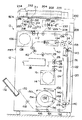
ここで、図2及び図3に示す如く、CCDラインセンサ230は、アナログ回路基板240に設けられている。このアナログ回路基板240は、レンズ226からの画像光がCCDラインセンサ230の受光面上に最適に結像するように位置調整されて固定されている。さらに、このアナログ回路基板240は、フレキシブルケーブル242によってデジタル回路基板244に電気的に接続されている。これにより、CCDラインセンサ230が撮像した画像光は、アナログ回路基板240によってアナログ画像信号に変換され、さらに、このアナログ画像信号はデジタル回路基板244によってデジタル画像信号に変換されて、原稿画像が画像データとして読取/記録される構成である。
【0020】
また、CCDラインセンサ230(アナログ回路基板240)の周囲には遮光カバー246が設けられており、CCDラインセンサ230を外部から遮光している。
【0021】
一方、ケーシング200上面には、プラテンガラス202の上を所定の隙間を持って主走査方向へ移動するプルーフ用光源ユニット232が配設されている。このプルーフ用光源ユニット232は、プラテンガラス202上に透過原稿が載置された場合の光源として適用されるものである。
【0022】
すなわち、このプルーフ用光源ユニット232は、その一端部(装置奥側)が光源ユニット駆動部234と連結されており、この光源ユニット駆動部234の駆動力により、前記第1のキャリッジ214と同等の動作を行う。
【0023】
ここで、透過原稿を走査する場合には、第1のキャリッジ214と同期がとられてプルーフ用光源ユニット232が動作する。このとき、第1のキャリッジ214の光源210は消灯しておき、プルーフ用光源ユニット232内の光源(図示省略)が点灯することにより、第1のミラー212で透過原稿画像を得ることができる。その後の動作は、反射原稿の場合と同様である。
(プリンタ部PRT)
図1には、画像読取/記録装置10の機台12内のプリンタ部PRTが示されている。
【0024】
機台12の内部には、感光材料16を収納する感材マガジン14が配置されており、感材マガジン14から引き出されたこの感光材料16の感光(露光)面が左方へ向くように感光材料16が感材マガジン14にロール状に巻き取られている。
【0025】
感材マガジン14の感光材料取出し口の近傍には、ニップローラ18およびカッタ20が配置されており、感材マガジン14から感光材料16を所定長さ引き出した後に切断することができる。カッタ20は、例えば固定刃と移動刃から成るロータリータイプのカッタとされており、移動刃を回転カム等によって上下に移動させて固定刃と噛み合わせ感光材料16を切断することができる。
【0026】
カッタ20の側方には、複数の搬送ローラ24、26、28、30、32、34が順に配置されており、各搬送ローラの間には図示しないガイド板が配設されている。所定長さに切断された感光材料16は、まず搬送ローラ24、26の間に設けられた露光部22へ搬送される。
【0027】
この露光部22の左側には露光装置38が設けられている。露光装置38には、3種のLD、レンズユニット、ポリゴンミラー、ミラーユニットが配置されており(何れも、図示省略)、露光装置38から光線Cが露光部22に送られて、感光材料16が露光されるようになっている。
【0028】
なお、LDをポリゴンミラーで振り子の如く走査する構成を用いず、LEDを主走査方向に配列して1ラインを同時に露光する構成であってもよい。
【0029】
さらに、露光部22の上方には、感光材料16をU字状に湾曲させて搬送するUターン部40及び画像形成用溶媒を塗布する為の水塗布部50が設けられている。尚、本実施の形態において画像形成用溶媒としては水が用いられる。
【0030】
感材マガジン14から上昇し露光部22にて露光された感光材料16は、搬送ローラ28、30によりそれぞれ挟持搬送されてUターン部40の上側寄りの搬送経路を通過しつつ水塗布部50へ送り込まれる。
【0031】
一方、機台12内の図1左上端部には受像材料108を収納する受材マガジン106が配置されている。この受像材料108の画像形成面には媒染剤を有する色素固定材料が塗布されており、受材マガジン106から引き出された受像材料108の画像形成面が下方へ向くように受像材料108が受材マガジン106にロール状に巻き取られている。
【0032】
受材マガジン106の受像材料取出し口の近傍には、ニップローラ110が配置されており、受材マガジン106から受像材料108を引き出すと共にそのニップを解除することができる。
【0033】
ニップローラ110の側方にはカッタ112が配置されている。カッタ112は前述の感光材料用のカッタ20と同様に、例えば固定刃と移動刃から成るロータリータイプのカッタとされており、移動刃を回転カム等によって上下に移動させて固定刃と噛み合わせることにより、受材マガジン106から引き出された受像材料108を感光材料16よりも短い長さに切断するようになっている。
【0034】
カッタ112の側方には、搬送ローラ132、134、136、138及び図示しないガイド板が配置されており、所定長さに切断された受像材料108を熱現像転写部120側に搬送できるようになっている。
【0035】
熱現像転写部120は、それぞれ複数の巻き掛けローラ140に巻き掛けられて、それぞれ上下方向を長手方向としたループ状にされた一対の無端ベルト122、124を有している。従って、これらの巻き掛けローラ140のいずれかが駆動回転されると、これらの巻き掛けローラ140に巻き掛けられた一対の無端ベルト122、124がそれぞれ回転される。
【0036】
これら一対の無端ベルト122、124の内の図上、右側の無端ベルト122のループ内には、上下方向を長手方向とした平板状に形成された加熱板126が、無端ベルト122の左側の内周部分に対向しつつ配置されている。この加熱板126の内部には、図示しない線状のヒータが配置されており、このヒータによって加熱板126の表面を昇温して所定の温度に加熱できるようになっている。
【0037】
従って、感光材料16は、搬送経路の最後の搬送ローラ34により熱現像転写部120の一対の無端ベルト122、124間に送り込まれる。また、受像材料108は感光材料16の搬送に同期して搬送され、感光材料16が所定長さ先行した状態で、搬送経路の最後の搬送ローラ138により熱現像転写部120の一対の無端ベルト122、124間に送り込まれて、感光材料16に重ね合わせられる。
【0038】
この場合、受像材料108は感光材料16よりも幅方向寸法および長手方向寸法がいずれも小さい寸法となっているため、感光材料16の周辺部は四辺とも受像材料108の周辺部から突出した状態で重ね合わせられることになる。
【0039】
以上より、一対の無端ベルト122、124によって重ね合わされた感光材料16及び受像材料108は、重ね合わせられた状態のままで一対の無端ベルト122、124によって挟持搬送されるようになる。さらに、重ね合わされた感光材料16と受像材料108が、一対の無端ベルト122、124間に完全に収まった時点で、一対の無端ベルト122、124は回転を一旦停止し、挟持した感光材料16と受像材料108を加熱板126で加熱する。感光材料16は、この挟持搬送時及び停止時において無端ベルト122を介して加熱板126により加熱されることとなり、加熱に伴って、可動性の色素を放出し、同時にこの色素が受像材料108の色素固定層に転写されて、受像材料108に画像が得られる構成である。
【0040】
さらに、一対の無端ベルト122、124に対して材料供給方向下流側には、剥離爪128が配置されており、この剥離爪128が一対の無端ベルト122、124間で挟持搬送される感光材料16と受像材料108のうち、感光材料16の先端部のみに係合し、一対の無端ベルト122、124間より突出したこの感光材料16の先端部を受像材料108から剥離させることができる。
【0041】
剥離爪128の左方には感材排出ローラ148が配置されており、剥離爪128に案内されながら左方へ移動される感光材料16を、更に廃棄感光材料収容部150側へ搬送し得るようになっている。
【0042】
この廃棄感光材料収容部150は、感光材料16が巻き付けられるドラム152及び、このドラム152に一部が巻き掛けられているベルト154を有している。さらに、このベルト154は複数のローラ156に巻き掛けられており、これらローラ156の回転によって、ベルト154が廻され、これに伴ってドラム152が回転するようになっている。
【0043】
従って、ローラ156の回転によりベルト154が廻された状態で、感光材料16が送り込まれると、感光材料16がドラム152の周りに集積できるようになっている。
【0044】
他方、一対の無端ベルト122、124の下方から左方に向かって受像材料108を搬送し得るように受材排出ローラ162、164、166、168、170が順に配置されており、一対の無端ベルト122、124から排出された受像材料108は、これら受材排出ローラ162、164、166、168、170によって搬送されて、トレイ172へ排出される構成である。
【0045】
以下に本実施の形態の作用を説明する。
まず、スキャナ部SCNにおける原稿画像の読取制御について説明する。
【0046】
画像の記録処理が開始される以前の状態においては、第1のキャリッジ214及び第2のキャリッジ220は画像記録領域を外れた待機位置(ホームポジション)に位置している。
【0047】
画像の記録処理を行うためにプラテンガラス202面上に原稿を載置し、押さえカバー204を閉じ、操作/表示パネルのキー操作によって読取開始が指示されると、スキャニングが開始される。
【0048】
このスキャニングでは、反射原稿の場合は光源210を点灯し、第1のキャリッジ214及び第2のキャリッジ220を同期させて動作を開始する。すなわち、第1のキャリッジ214及び第2のキャリッジ220が原稿面に沿って副走査方向に往復移動する。この際には、第1のキャリッジ214の搬送速度V1 と、第2のキャリッジ220の搬送速度V2 との関係は、V1 =2V2 である。これを維持することによって、原稿画像面からCCDラインセンサ230の受光面までの光路長を常に一定に維持することができる。
【0049】
スキャニングによってCCDラインセンサ230が撮像した画像光は、アナログ回路基板240によってアナログ画像信号に変換され、さらに、このアナログ画像信号はデジタル回路基板244によってデジタル画像信号に変換されて、原稿画像が画像データとして得られる。さらに、この得られた画像データは、パソコン等のRAMメモリやハードディスクに記録され、所定の画像処理が施された後、プリンタ部PRTへ送られる。
【0050】
ここで、このスキャナ部SCNにおいては、画像データを得るための画像読取系が、CCDラインセンサ230が設けられたアナログ回路基板240とデジタル回路基板244とに二分割されて構成されるため、各回路基板の配置位置等に制限を受け難くなり、装置のスペースを有効に利用することができる。すなわち、各回路基板のために装置の大きさが制限を受け難くなり、したがって装置を最小限に小型化することが可能になる。
【0051】
また、アナログ回路基板240とデジタル回路基板244とはフレキシブルケーブル242によって電気的に接続された構成であるため、レンズ226からの画像光がCCDラインセンサ230の受光面上に最適に結像するようにアナログ回路基板240を位置調整する際に、各部に不要な力が加わることがなく、また位置調整のための作業性も向上する。
【0052】
またこの場合、CCDラインセンサ230(アナログ回路基板240)の周囲に設けられた遮光カバー246に若干の隙間を設けると共に、この隙間を遮光性のスポンジ等によって塞いでおけば、前記CCDラインセンサ230(アナログ回路基板240)の位置調整のために各装置毎に取付け位置のバラツキが生じても、CCDラインセンサ230(アナログ回路基板240)と遮光カバー246とが干渉することがなく、好適に取り付けることができる。
【0053】
次に、プリンタ部PRTの動作を説明する。
感材マガジン14がセットされた後には、ニップローラ18が作動され、感光材料16がニップローラ18によって引き出される。感光材料16が所定長さ引き出されると、カッタ20が作動して、感光材料16が所定長さに切断されると共に、その感光(露光)面を左方へ向けた状態で露光部22へ搬送される。そして、この感光材料16の露光部22の通過と同時に露光装置38が作動し、露光部22に位置する感光材料16へ画像が走査露光される。露光装置38には、前述したスキャナSCN部で読み取った画像データがパソコンで画像処理されて入力されており、この入力されたデータに基づいて光源の光量が制御され、画像が走査露光される。光源としては、レーザ(半導体レーザ)を用いる場合には、デューティ制御によって光量が制御されたレーザビームの光軸を振り子の如く往復移動させることにより主走査を行い、感光材料16の移動を副走査とすればよい。
【0054】
また、光源として、LED等の主走査方向に配列してLEDアレイを用いる場合には、LED光源を電流又は電圧制御して光量を制御し、1主走査を同時期に行うようにすればよい。
【0055】
露光が終了すると、露光後の感光材料16は、水塗布部50に送られる。水塗布部50において画像形成用溶媒としての水が塗布された感光材料16は、搬送ローラ34によって熱現像転写部120の一対の無端ベルト122、124間へ送り込まれる。
【0056】
他方、感光材料16へ走査露光されるに伴って、受像材料108も受材マガジン106からニップローラ110によって引き出されて搬送される。受像材料108が所定長さ引き出されると、カッタ112が作動して受像材料108が所定長さに切断される。
【0057】
カッタ112の作動後は、切断された受像材料108がガイド板によって案内されながら搬送ローラ132、134、136、138によって搬送される。受像材料108の先端部が搬送ローラ138によって挟持されると、受像材料108は熱現像転写部120の直前で待機状態となる。
【0058】
そして、前述のように感光材料16が搬送ローラ34によって一対の無端ベルト122、124間へ送り込まれるのに伴って、受像材料108の搬送が再開されて、一対の無端ベルト122、124間へ受像材料108が感光材料16と一体的に送り込まれる。
【0059】
この結果、感光材料16と受像材料108が重ねられ、感光材料16と受像材料108とが加熱板126により加熱されつつ挟持搬送されて、熱現像転写を行って画像が受像材料108に形成される。
【0060】
さらに、一対の無端ベルト122、124からこれらが排出されると、受像材料108よりも所定長さ先行して搬送される感光材料16の先端部に剥離爪128が係合し、感光材料16の先端部を受像材料108から剥離する。この感光材料16は、さらに感材排出ローラ148によって搬送され、廃棄感光材料収容部150内に集積される。この際、感光材料16はすぐに乾燥するので、感光材料16を乾燥させる為に、ヒータ類をさらに設ける必要はない。
【0061】
一方、一対の無端ベルト122、124に挟まれて熱現像転写処理されて所定の画像が形成(記録)された受像材料108は、一対の無端ベルト122、124から排出された後に、複数の受材排出ローラ162、164、166、168、170によって挟持搬送されて装置外のトレイ172へ排出される。
【0062】
そして、複数枚の画像記録処理を実施する場合には、以上の工程が順次連続して行なわれる。
【0063】
以上の如く、本実施の形態に係る画像読取/記録装置10では、画像データを得るためのスキャナ部SCNにおける画像読取系が、CCDラインセンサ230が設けられたアナログ回路基板240とデジタル回路基板244とに二分割されて構成されるため、装置のスペースを有効に利用することができ、装置を最小限に小型化することが可能になる。
【0064】
また、アナログ回路基板240とデジタル回路基板244とはフレキシブルケーブル242によって電気的に接続された構成であるため、アナログ回路基板240(CCDラインセンサ230)を位置調整する際やその後に、各部に不要な力が加わることがなく、また位置調整のための作業性も向上する。
【0065】
【発明の効果】
以上説明した如く本発明に係る画像記録装置では、装置を最小限に小型化することが可能になるという優れた効果を有している。
【図面の簡単な説明】
【図1】本発明の実施の形態に係る画像記録装置の概略全体構成図である。
【図2】本発明の実施の形態に係る画像記録装置のアナログ回路基板及びデジタル回路基板の正面図である。
【図3】本発明の実施の形態に係る画像記録装置のアナログ回路基板及びデジタル回路基板の図2に対応する斜視図である。
【符号の説明】
10 画像読取/記録装置
SCN スキャナ部
PRT プリンタ部
208 走査部
210 光源
214 第1のキャリッジ
220 第2のキャリッジ
228 固定ユニット
230 CCDラインセンサ(固体撮像素子)
240 アナログ回路基板
242 フレキシブルケーブル
244 デジタル回路基板
246 遮光カバー[0001]
BACKGROUND OF THE INVENTION
The present invention relates to an image reading apparatus, and more particularly, to read an image light from a document with a solid-state imaging device and convert it into an analog image signal, and then convert the analog image signal into a digital image signal for recording an image. Relates to the device.
[0002]
[Prior art]
2. Description of the Related Art There is known an image reading apparatus that irradiates a document image with light, reads reflected or transmitted light with a CCD sensor, and records the document image as image data.
[0003]
In this type of image reading apparatus, light is irradiated onto a document, and image light (reflected or transmitted light) from the document is guided to a CCD sensor through a lens, whereby the image light is captured and converted into an analog image signal. Converted. Furthermore, the original image is read / recorded as image data by converting the analog image signal into a digital image signal.
[0004]
By the way, in such a conventional image reading apparatus, a circuit board provided with a CCD sensor and having a digital conversion unit for converting an analog image signal into a digital image signal is configured as a single product. There is a drawback that the arrangement position is limited or the physique of the device is determined by the circuit board, and as a result, the space cannot be used effectively and the physique of the device is enlarged. In other words, the size of the device is easily limited due to the circuit board, and it is difficult to miniaturize the device to the minimum, and a countermeasure for this is desired.
[0005]
[Problems to be solved by the invention]
In view of the above facts, an object of the present invention is to obtain an image reading apparatus capable of miniaturizing the apparatus to the minimum.
[0006]
[Means for Solving the Problems]
An image reading apparatus according to a first aspect of the invention reads an image light from a document with a solid-state image sensor and converts it into an analog image signal, and then converts the analog image signal into a digital image signal for recording an image. In the reading device, the circuit board of the image reading device is provided with the solid-state image sensor and an analog circuit board provided with circuit components for converting image light read by the solid-state image sensor into an analog image signal; Dividing the analog image signal into a digital circuit board provided with a circuit component for converting the analog image signal into a digital image signal, and electrically connecting the analog circuit board and the digital circuit board by a flexible cable ; and A light shielding cover is provided around the analog circuit board, and the analog circuit board and the light shielding cover In a gap, it plugged by a member having a light shielding property and flexibility the gap, and characterized in that.
[0007]
According to the first aspect of the present invention, since the circuit board of the image reading apparatus is divided into the analog circuit board and the digital circuit board, the arrangement position of each circuit board is not easily limited, The space of the apparatus can be used effectively. That is, the size of the device is less likely to be limited for each circuit board, and thus the device can be miniaturized to a minimum.
[0008]
DETAILED DESCRIPTION OF THE INVENTION
FIG. 1 shows a schematic overall configuration diagram of an image reading /
[0009]
The image reading /
(Scanner section SCN)
FIG. 1 shows a scanner unit SCN according to the present embodiment.
[0010]
The scanner unit SCN is covered with a box-
[0011]
On the
[0012]
Therefore, when the
[0013]
An operation / display panel (not shown) is disposed on the front side of the upper surface of the
[0014]
A
[0015]
As shown in detail in FIGS. 2 and 3, the
[0016]
A
[0017]
On the other hand, the
[0018]
The
[0019]
Here, as shown in FIGS. 2 and 3, the
[0020]
A
[0021]
On the other hand, on the upper surface of the
[0022]
That is, the proof
[0023]
Here, when scanning a transparent original, the proof
(Printer part PRT)
FIG. 1 shows a printer unit PRT in the
[0024]
A
[0025]
A nip roller 18 and a
[0026]
A plurality of
[0027]
An
[0028]
Instead of using a configuration in which the LD is scanned like a pendulum by a polygon mirror, a configuration in which LEDs are arranged in the main scanning direction and one line is simultaneously exposed may be used.
[0029]
Further, above the exposure unit 22, a
[0030]
The
[0031]
On the other hand, a receiving
[0032]
A nip roller 110 is disposed in the vicinity of the image receiving material take-out port of the image receiving
[0033]
A
[0034]
Conveying
[0035]
The thermal development transfer unit 120 includes a pair of
[0036]
Within the loop of the right
[0037]
Accordingly, the
[0038]
In this case, since the image receiving material 108 is smaller than the
[0039]
As described above, the
[0040]
Further, a peeling
[0041]
A photosensitive
[0042]
The waste
[0043]
Accordingly, when the
[0044]
On the other hand, receiving
[0045]
The operation of this embodiment will be described below.
First, document image reading control in the scanner unit SCN will be described.
[0046]
In a state before the image recording process is started, the
[0047]
When an original is placed on the
[0048]
In this scanning, in the case of a reflection original, the
[0049]
The image light captured by the
[0050]
Here, in this scanner unit SCN, an image reading system for obtaining image data is divided into an
[0051]
Further, since the
[0052]
In this case, if the
[0053]
Next, the operation of the printer unit PRT will be described.
After the
[0054]
Further, when an LED array is used as a light source arranged in the main scanning direction such as an LED, the amount of light may be controlled by controlling the LED light source by current or voltage to perform one main scanning at the same time. .
[0055]
When the exposure is completed, the exposed
[0056]
On the other hand, as the
[0057]
After the
[0058]
Then, as the
[0059]
As a result, the
[0060]
Further, when these are discharged from the pair of
[0061]
On the other hand, the image receiving material 108 on which a predetermined image is formed (recorded) between the pair of
[0062]
When a plurality of image recording processes are performed, the above steps are sequentially performed.
[0063]
As described above, in the image reading /
[0064]
Further, since the
[0065]
【The invention's effect】
As described above, the image recording apparatus according to the present invention has an excellent effect that the apparatus can be miniaturized to a minimum.
[Brief description of the drawings]
FIG. 1 is a schematic overall configuration diagram of an image recording apparatus according to an embodiment of the present invention.
FIG. 2 is a front view of an analog circuit board and a digital circuit board of the image recording apparatus according to the embodiment of the present invention.
3 is a perspective view corresponding to FIG. 2 of an analog circuit board and a digital circuit board of the image recording apparatus according to the embodiment of the present invention.
[Explanation of symbols]
10 Image Reading / Recording Device SCN Scanner Unit
240
Claims (1)
該画像読取装置の回路基板を、前記固体撮像素子が設けられると共に前記固体撮像素子により読み取った画像光をアナログ画像信号に変換するための回路部品が設けられたアナログ回路基板と、前記アナログ画像信号をデジタル画像信号に変換するための回路部品が設けられたデジタル回路基板とに二分割し、かつ前記アナログ回路基板とデジタル回路基板とをフレキシブルケーブルによって電気的に接続し、かつ前記アナログ回路基板の周囲に遮光カバーを設けると共に、前記アナログ回路基板と前記遮光カバーとの間に隙間を設け、当該隙間を遮光性及び可撓性を有する部材により塞いだ、ことを特徴とする画像読取装置。In an image reading device that reads image light from a document with a solid-state image sensor and converts it into an analog image signal, and then converts the analog image signal into a digital image signal for recording an image.
An analog circuit board provided with a circuit component for converting image light read by the solid-state image sensor into an analog image signal, and the analog image signal provided on the circuit board of the image reading device Is divided into a digital circuit board provided with a circuit component for converting the digital image signal into a digital image signal, and the analog circuit board and the digital circuit board are electrically connected by a flexible cable , and the analog circuit board An image reading apparatus characterized in that a light shielding cover is provided around, a gap is provided between the analog circuit board and the light shielding cover, and the gap is closed with a light shielding and flexible member .
Priority Applications (1)
| Application Number | Priority Date | Filing Date | Title |
|---|---|---|---|
| JP17468497A JP3662717B2 (en) | 1997-06-30 | 1997-06-30 | Image reading device |
Applications Claiming Priority (1)
| Application Number | Priority Date | Filing Date | Title |
|---|---|---|---|
| JP17468497A JP3662717B2 (en) | 1997-06-30 | 1997-06-30 | Image reading device |
Publications (2)
| Publication Number | Publication Date |
|---|---|
| JPH1127442A JPH1127442A (en) | 1999-01-29 |
| JP3662717B2 true JP3662717B2 (en) | 2005-06-22 |
Family
ID=15982894
Family Applications (1)
| Application Number | Title | Priority Date | Filing Date |
|---|---|---|---|
| JP17468497A Expired - Fee Related JP3662717B2 (en) | 1997-06-30 | 1997-06-30 | Image reading device |
Country Status (1)
| Country | Link |
|---|---|
| JP (1) | JP3662717B2 (en) |
Families Citing this family (2)
| Publication number | Priority date | Publication date | Assignee | Title |
|---|---|---|---|---|
| JP4155782B2 (en) * | 2002-09-20 | 2008-09-24 | 株式会社リコー | Reading unit, image reading apparatus, and image forming apparatus |
| JP4615499B2 (en) * | 2006-09-29 | 2011-01-19 | 京セラミタ株式会社 | Image reading apparatus and image forming apparatus |
-
1997
- 1997-06-30 JP JP17468497A patent/JP3662717B2/en not_active Expired - Fee Related
Also Published As
| Publication number | Publication date |
|---|---|
| JPH1127442A (en) | 1999-01-29 |
Similar Documents
| Publication | Publication Date | Title |
|---|---|---|
| JP3662717B2 (en) | Image reading device | |
| US4864352A (en) | Image recording apparatus and system | |
| JP3903091B2 (en) | Image reading device | |
| JP2863674B2 (en) | Image forming device | |
| JP3784922B2 (en) | Image reading device | |
| JP2867837B2 (en) | Imaging equipment | |
| JPH1124180A (en) | Original platen | |
| JP3734929B2 (en) | Image reading device | |
| JPH10333259A (en) | Image recorder | |
| US6115103A (en) | Scanning-exposure apparatus | |
| JPH1138523A (en) | Image reader | |
| JPH10322515A (en) | Image reader | |
| US6140629A (en) | Image reading method and image reading apparatus | |
| JPH10308859A (en) | Image reading and recording device | |
| JP2851922B2 (en) | Paper feeder | |
| JP3540383B2 (en) | Image recording device | |
| JPH1164996A (en) | Image reader | |
| JPS6363275A (en) | Reader | |
| JPH1138524A (en) | Image reader | |
| JPH09146182A (en) | Image forming device | |
| JPH07295115A (en) | Illumination light source device | |
| JPH086174A (en) | Image reader | |
| JPH10336384A (en) | Image reader | |
| JP2791713B2 (en) | Image reading device | |
| JP2957814B2 (en) | Image forming device |
Legal Events
| Date | Code | Title | Description |
|---|---|---|---|
| A977 | Report on retrieval |
Free format text: JAPANESE INTERMEDIATE CODE: A971007 Effective date: 20041213 |
|
| A131 | Notification of reasons for refusal |
Free format text: JAPANESE INTERMEDIATE CODE: A131 Effective date: 20041228 |
|
| A521 | Written amendment |
Free format text: JAPANESE INTERMEDIATE CODE: A523 Effective date: 20050217 |
|
| TRDD | Decision of grant or rejection written | ||
| A01 | Written decision to grant a patent or to grant a registration (utility model) |
Free format text: JAPANESE INTERMEDIATE CODE: A01 Effective date: 20050322 |
|
| A61 | First payment of annual fees (during grant procedure) |
Free format text: JAPANESE INTERMEDIATE CODE: A61 Effective date: 20050324 |
|
| R150 | Certificate of patent or registration of utility model |
Free format text: JAPANESE INTERMEDIATE CODE: R150 |
|
| S111 | Request for change of ownership or part of ownership |
Free format text: JAPANESE INTERMEDIATE CODE: R313111 |
|
| FPAY | Renewal fee payment (event date is renewal date of database) |
Free format text: PAYMENT UNTIL: 20080401 Year of fee payment: 3 |
|
| R350 | Written notification of registration of transfer |
Free format text: JAPANESE INTERMEDIATE CODE: R350 |
|
| FPAY | Renewal fee payment (event date is renewal date of database) |
Free format text: PAYMENT UNTIL: 20090401 Year of fee payment: 4 |
|
| FPAY | Renewal fee payment (event date is renewal date of database) |
Free format text: PAYMENT UNTIL: 20090401 Year of fee payment: 4 |
|
| FPAY | Renewal fee payment (event date is renewal date of database) |
Free format text: PAYMENT UNTIL: 20100401 Year of fee payment: 5 |
|
| LAPS | Cancellation because of no payment of annual fees |