JP3661852B2 - Protected microprocessor with system for assigning rights to the library - Google Patents
Protected microprocessor with system for assigning rights to the library Download PDFInfo
- Publication number
- JP3661852B2 JP3661852B2 JP2001195422A JP2001195422A JP3661852B2 JP 3661852 B2 JP3661852 B2 JP 3661852B2 JP 2001195422 A JP2001195422 A JP 2001195422A JP 2001195422 A JP2001195422 A JP 2001195422A JP 3661852 B2 JP3661852 B2 JP 3661852B2
- Authority
- JP
- Japan
- Prior art keywords
- subprogram
- microprocessor
- program
- address
- rights
- Prior art date
- Legal status (The legal status is an assumption and is not a legal conclusion. Google has not performed a legal analysis and makes no representation as to the accuracy of the status listed.)
- Expired - Fee Related
Links
- 230000015654 memory Effects 0.000 claims description 48
- 230000006870 function Effects 0.000 claims description 7
- 238000012545 processing Methods 0.000 claims description 2
- 235000013399 edible fruits Nutrition 0.000 claims 1
- 102100033270 Cyclin-dependent kinase inhibitor 1 Human genes 0.000 description 15
- 108091006627 SLC12A9 Proteins 0.000 description 15
- 102100034770 Cyclin-dependent kinase inhibitor 3 Human genes 0.000 description 12
- 101100439050 Homo sapiens CDKN3 gene Proteins 0.000 description 12
- 101150089280 cip2 gene Proteins 0.000 description 12
- 102100026190 Class E basic helix-loop-helix protein 41 Human genes 0.000 description 9
- 101000765033 Homo sapiens Class E basic helix-loop-helix protein 41 Proteins 0.000 description 9
- 102100026064 Exosome complex component RRP43 Human genes 0.000 description 6
- 101001055989 Homo sapiens Exosome complex component RRP43 Proteins 0.000 description 6
- 101100369068 Saccharomyces cerevisiae (strain ATCC 204508 / S288c) TDA1 gene Proteins 0.000 description 6
- 102100026191 Class E basic helix-loop-helix protein 40 Human genes 0.000 description 5
- 101710130550 Class E basic helix-loop-helix protein 40 Proteins 0.000 description 5
- 238000010586 diagram Methods 0.000 description 4
- UCTWMZQNUQWSLP-VIFPVBQESA-N (R)-adrenaline Chemical compound CNC[C@H](O)C1=CC=C(O)C(O)=C1 UCTWMZQNUQWSLP-VIFPVBQESA-N 0.000 description 3
- 101000854862 Homo sapiens Vacuolar protein sorting-associated protein 35 Proteins 0.000 description 3
- 101150086208 TDA2 gene Proteins 0.000 description 3
- 102100020822 Vacuolar protein sorting-associated protein 35 Human genes 0.000 description 3
- 230000008901 benefit Effects 0.000 description 3
- 238000012546 transfer Methods 0.000 description 3
- 238000004364 calculation method Methods 0.000 description 2
- 101100480850 Saccharomyces cerevisiae (strain ATCC 204508 / S288c) TDA3 gene Proteins 0.000 description 1
- 230000006399 behavior Effects 0.000 description 1
- 239000011159 matrix material Substances 0.000 description 1
- 238000000034 method Methods 0.000 description 1
- 238000005192 partition Methods 0.000 description 1
- 238000000638 solvent extraction Methods 0.000 description 1
- 238000010561 standard procedure Methods 0.000 description 1
- 238000012795 verification Methods 0.000 description 1
Images


Classifications
-
- G—PHYSICS
- G06—COMPUTING; CALCULATING OR COUNTING
- G06F—ELECTRIC DIGITAL DATA PROCESSING
- G06F12/00—Accessing, addressing or allocating within memory systems or architectures
- G06F12/14—Protection against unauthorised use of memory or access to memory
- G06F12/1416—Protection against unauthorised use of memory or access to memory by checking the object accessibility, e.g. type of access defined by the memory independently of subject rights
- G06F12/1425—Protection against unauthorised use of memory or access to memory by checking the object accessibility, e.g. type of access defined by the memory independently of subject rights the protection being physical, e.g. cell, word, block
- G06F12/1441—Protection against unauthorised use of memory or access to memory by checking the object accessibility, e.g. type of access defined by the memory independently of subject rights the protection being physical, e.g. cell, word, block for a range
-
- G—PHYSICS
- G06—COMPUTING; CALCULATING OR COUNTING
- G06F—ELECTRIC DIGITAL DATA PROCESSING
- G06F12/00—Accessing, addressing or allocating within memory systems or architectures
- G06F12/14—Protection against unauthorised use of memory or access to memory
- G06F12/1458—Protection against unauthorised use of memory or access to memory by checking the subject access rights
- G06F12/1483—Protection against unauthorised use of memory or access to memory by checking the subject access rights using an access-table, e.g. matrix or list
Description
【0001】
【発明の属する技術分野】
本発明は、マイクロプロセッサに関し、特に、保護されたマイクロプロセッサに関するものである。
【0002】
保護されたマイクロプロセッサは、ある機密データやプログラムへのアクセスが禁止される必要があるアプリケーションにおいて、最も一般的に用いらている。従って、機密コードや暗号文アルゴリズムを備えたメモリゾーンを保護するために、例えばスマートカードが一般に保護されたマイクロプロセッサに備えられている。
【0003】
【従来の技術】
従来、マイクロプロセッサは、実行されているプログラムが、読み取り、書き込み、ジャンプ、または呼出し動作のために、あるメモリゾーンをアドレス指定する資格が与えられていることを確認するアドレス制御システムによって保護されている。この種のシステムは、一般に、実行されているプログラムの識別コードを第1の入力にて受信し、アドレス指定されているメモリゾーンの識別コードを第2の入力にて受信する権利割り当てテーブルである。前記メモリゾーンは、マイクロプロセッサのアドレスバスに存在する現在のアドレスに対応する。テーブルにおいて、実行されているプログラムがアドレス指定されているメモリゾーンを利用可能であると予定されている場合、前記テーブルは許可信号を出力する。そうでない場合、前記テーブルは許可信号を出力せず、アドレス違反信号が送信される。
【0004】
この種のアドレス制御システムは、マイクロプロセッサのメモリアレイ内の様々なプログラムの保護された共存を、それらのプログラムの各々に異なる権利を割り当てることによって得るために用いられる。これらの様々なプログラムは、一般に、メーカーによって予定された、マイクロプロセッサの異なるアプリケーションに対応している。
【0005】
【発明が解決しようとする課題】
しかしながら、マイクロプロセッサの保護は、メモリアレイを、各部分が一つのアプリケーションのために確保されている、様々な相互に“密閉された”部分に分割するという点において、メモリアレイの構成にマイナスの影響を及ぼす。現在、異なるアプリケーションのために設計されたプログラムが、“ライブラリ”としての、ある共通領域に集中化できるような類似した計算ステップを有していることがよくある。ライブラリとは,当業者の用語では、いくつかのプログラムによって共用される、一つ以上のサブプログラムを示す。
【0006】
いくつかのプログラムに共通なライブラリ形式のプログラム部分への集中化の標準的な方法は、それが引き起こす安全性の問題のために、保護されたマイクロプロセッサに対しては、一般に禁止されている。例えば,プログラムPGAはメモリアレイのゾーン“X”へアクセスする権利を享受し、 プログラムPGBは “X”と異なるゾーン“Y”へアクセスする権利を享受すると仮定する。プログラムPGAとプログラムPGBによって共用されるサブプログラムを設計することは、どちらがサブプログラムに与えられるべき権利であるかを見つけるという問題を招く。サブプログラムが、プログラムPGAに呼び出された時にはゾーン”X”のデータを読み取ったり書き込んだりすることができ、プログラムPGBに呼び出された時にはゾーン“Y”のデータを読み取ったり書き込んだりすることができる必要がある場合、サブプログラムは、プログラムPGAおよびPGBの総合された権利、すなわち、ゾーン“X”とゾーン“Y”に対する権利を与えられなければならない。しかしながら、プログラムPGB、またはプログラムPGBの場所にロードされた不正プログラムは、サブプログラムを使用して、プログラムPGAのために確保されているゾーン“X”へアクセスすることができるかもしれないし、その逆もまた同様である。従って、メモリアレイへの異なるアクセス権を有する二つのプログラムによって共用されるサブプログラムを設計することは、メモリアレイの分割における違反である。
【0007】
本発明は、この欠点を克服しようとするものである。
【0008】
特に、本発明は、いくつかのプログラムによって共用されるサブプログラムを、そのプログラムの各々に与えられた権利の完全性を危うくすることなく提供するための手段を得ようとするものである。
【0009】
【課題を解決するための手段】
この目的は、マイクロプロセッサによって実行可能なプログラムに、マイクロプロセッサのメモリアレイの、あるゾーンへの永続的なアクセス権を割り当てるための権利割り当てシステムを備えた保護されたマイクロプロセッサを設計することによって達成され、該権利割り当てシステムは、少なくとも2つのプログラムによって共用されるサブプログラムに対して、該サブプログラムがそれらのプログラムの一つによって呼び出される場合、あるメモリゾーンへの一時的なアクセス権を与える手段を備え、その一時的な権利の範囲は、サブプログラムを呼び出しているプログラムの機能であることを特徴とするものである。
【0010】
ある実施の形態によれば、この権利割り当てシステムは、サブプログラムに対して呼出しプログラムの権利を一時的に与える手段を備える。
【0011】
ある実施の形態によれば、この権利割り当てシステムは、サブプログラムに対して、呼出しプログラムとは独立した永続的な権利をさらに与える手段を備える。
【0012】
ある実施の形態によれば、この権利割り当てシステムは、第1の入力においてプログラムまたはサブプログラムの識別コードを、第2の入力においてマイクロプロセッサのアドレスバスを流れる現在のアドレスによって指定されたメモリゾーンの識別コードを受信するためにレイアウトされた権利割り当てテーブルと、サブプログラムの実行中に、権利割り当てテーブルの第1の入力に、サブプログラムを呼び出したプログラムの識別コードを入力する手段とを備える。
【0013】
ある実施の形態によれば、この権利割り当てシステムは、サブプログラムの実行中に、権利割り当てテーブルの第1の入力に、実行されているサブプログラムの識別コードと、前記サブプログラムを呼び出したプログラムの識別コードとを、同時に入力する手段を備える。
【0014】
ある実施の形態によれば、実行されているサブプログラムの識別コードのビットと、前記サブプログラムを呼び出したプログラムの識別コードのビットが、権利割り当てテーブルの第1の入力に入力される前に論理機能によって結合される。
【0015】
ある実施の形態によれば、この権利割り当てシステムは、命令の実行中に、実行されているプログラムまたはサブプログラムの識別コードを格納するための第1のラッチと、その入力が第1のラッチの出力に接続され、マイクロプロセッサがサブプログラムに切り換える時に実行されているプログラムの識別コードを格納するようにレイアウトされて、このサブプログラムを呼び出したプログラムの識別コードを形成する第2のラッチとを備え、前記第2のラッチは、マイクロプロセッサが前記サブプログラムを終了するとリセットされる。
【0016】
ある実施の形態によれば、前記第2のラッチのローディング及びリセットは、アドレスバスを流れる電流アドレスを入力において受信し、サブプログラムの第1の命令のアドレスが検出されると、ローディング信号を前記第2のラッチに入力するようにレイアウトされ、サブプログラムの最後の命令のアドレスが検出されると、リセット信号を第2のラッチに送信するアドレスデコーダによって制御される。
【0017】
ある実施の形態によれば、現在のアドレスによって指定されるメモリゾーンの識別コードと、実行されているプログラムおよびサブプログラムの識別コードとは、アドレスバスを流れる現在のアドレスを入力において受信するアドレスデコーダによって送信される。
【0018】
ある実施の形態によれば、権利分配システムは、アドレスバスに存在するアドレスが、実行されているプログラムまたはサブプログラムに永続的にまたは一時的に割り当てられる権利に対応しない場合、違反信号を送信する。
【0019】
ある実施の形態によれば、前記違反信号は、割り込みデコーダによって処理されて、マイクロプロセッサをアドレス違反処理サブプログラムに送る。
【0020】
【発明の実施の形態】
本発明のこれらおよび他の目的、特徴および利点は、本発明によるマイクロプロセッサの例示的な実施形態に関する、非限定的な説明として与えられ、添付の図を参照してなされる以下の説明において、さらに詳細に説明される。
【0021】
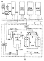
図1は、読み出し専用メモリMEM1(ROM)と、電気的消去可能プログラム可能メモリMEM2 (EEPROM)と、ランダムアクセスメモリMEM3 (RAM)とを備えつけられたマイクロプロセッサMPのブロック図である。これらの様々なメモリは、アドレスバス1およびデータバス2によってマイクロプロセッサに接続され、ともにマイクロプロセッサのメモリアレイを形成している。
【0022】
本発明によれば、マイクロプロセッサMPは、呼出しプログラムの機能として、サブプログラムに対し可変アクセス権を与える権利割り当てシステム10を備えている。
【0023】
システム10は、入力においてアドレスバスに接続されて、アドレスバスを循環している現在のアドレスADRを受信する2つのアドレスデコーダDEC1およびDEC2を備えている。デコーダDEC1は、メモリゾーン識別のための以下のようなタイプのコードCIM を出力する:
CIM = b0 b1...bn bn+1...bm
ここで、各ビットは所定のメモリゾーンの識別に割り当てられており、一度に1つのビットのみが1になることができ、他は0になる。
【0024】
以下、ビットb0ないしbnはメモリからなるメモリゾーンの指定に割り当てられており、ビットbn+1ないしbmはデータからなるメモリゾーンの指定に割り当てられているとする。メモリゾーンは、例えばメモリMEM1に配置され、データゾーンは、メモリMEM2およびMEM3に配置されている。
【0025】
コードCIMのビットb0ないしbnは、マイクロプロセッサMPより出力されるローディング信号LOAD1によって駆動されるラッチLT1の入力に入力される。信号LOAD1がラッチLT 1に入力されると、ラッチの出力は、該ラッチの入力を複写し、プログラムゾーン識別のためのコードCIP1を出力する。
【0026】
コードCIP1 は、デコーダDEC2より出力されるローディング信号LOAD2およびリセット信号RSTによって駆動される第2のラッチLT2の入力に入力される。信号LOAD2がラッチLT2に入力されると、ラッチLT2の出力は、その入力にあるコードCIP1を複写するコードCIP2を出力する。
【0027】
コードCIP1およびCIP2は結合されて、その結果コードCIP3を形成し、これは、デコーダDEC1より出力されるコードCIMを入力E2において受信する権利割り当てテーブルTDAの入力E1に入力される。本実施の形態では、コードCIP1およびCIP2の結合はORゲート11によって提供され、その出力は、コードCIP1およびCIP2のビット毎の論理和に等しいコードCIP3を出力する。
【0028】
権利割り当てテーブルTDAは、基本出力S0〜Sn からなる出力OUTを備え、各出力S0〜Sn は、コードCIP3のビットの一つを受信する入力E1の基本入力E11, …, E1nの同順位のものに対応している。出力S0〜S nは、許可ビットa0〜an という形でアクセス権を出力する。許可ビットaiは、対応する入力E1iが1ビットに等しいビットbiを受信した時は1ビットに等しく、ビットbi と共に、1ビットである許可された組み合わせ{bi,bj}を形成する。許可された組み合わせ{bi,bj}は、最終的にテーブルに記録され、永続的な権利を定める。
【0029】
ラッチLT1のローディング信号LOAD1は、マイクロプロセッサMPがメモリMEM1内の命令を読み取る時、またはまさに読み取ろうとしている時(マイクロプロセッサの読み取りサイクルまたはフェッチサイクル)に、マイクロプロセッサMPから送信される。その時点で、アドレスバスに存在するアドレスADRは、マイクロプロセッサの順序カウンタPCより送信される命令のアドレスIADRである。従って、デコーダDEC1より送信されるコードCIMは、この命令を有するメモリゾーンを指定するビットbi ないし1を有する。このビットbiは、ラッチLT1に記録されているコードCIP1、およびテーブルTDAの入力E1において見つけられる。
【0030】
さらに、信号LOAD2は、デコーダDEC2が共用サブプログラムの第1の命令のアドレスADRinをバス1上において検出すると、デコーダDEC2より送信され、信号RSTは、デコーダDEC2が共用サブプログラムの最後の命令のアドレスADRoutをアドレスバス上において検出すると、デコーダDEC2より送信される。アドレスADRinおよびADRoutは予め設定されており、考慮されているサブプログラムの入力アドレスおよび出力アドレスを表わしている。いくつかのサブプログラムが複数のプログラムによって共用されている場合、デコーダDEC2は、各サブプログラムの入力アドレスおよび出力アドレスを検出し、これらのアドレスの一方が検出されると信号LOAD2または信号RSTを送信するようにレイアウトされる。
【0031】
本発明によるシステム10は、ラッチLT2の出力が0で、テーブルTDAに入力されるコードCIP3は従ってコードCIP1に等しいので、プログラムの実行中は従来通りに作動する。プログラムの実行中、それぞれの新たな命令のローディングの後、例えば実行されている命令がメモリアレイにおける読み取りまたは書き込み命令であるとき、アドレスバスの現在のアドレスADRが変化し、メモリの他のゾーンを指定することがしばしばある。この場合、デコーダDEC1より送信されたコードCIMの値が変化し、対応するメモリゾーンを指定する、1である異なるビットbjを有する。テーブルTDAに入力される組み合わせ{bi,bj}が許可される場合、テーブルの出力Siは1のままである。さもなければ、出力Si は0になり、違反信号VLTは1になる。この命令の実行後、新たな命令のアドレスIADRがアドレスバスに送られ、コードCIMのさらなる変化およびコードビットの他の組み合わせ{bi,bj}のテーブルTDAにおける自動的な検証を引き起こす。このアドレスがサブプログラムにおけるジャンプに対応する場合、テーブルTDAにおいて対応する許可が予定されなければならない。
【0032】
本発明によるシステム10の動作は、プログラムが、共用サブプログラムに対するジャンプや呼び出しのための命令を有するとき、標準的なアドレス制御システムとは異なる。サブプログラムの第1の命令のアドレスADRinがアドレスバス上に位置している時、デコーダDEC2は信号LOAD2を送信し、ラッチLT2は、マイクロプロセッサがサブプログラムに切り換える前にコードCIP1を記録する。マイクロプロセッサがサブプログラムに切り換えると、ラッチLT1の出力におけるコードCIP1は、サブプログラムを含むメモリゾーンを指定し、ラッチLT2の出力におけるコードCIP2は、このサブプログラムを呼び出したプログラムが、あるメモリゾーンを指定する。こうして、コードCIP1は、実行されているサブプログラムを識別し、コードCIP2は、このサブプログラムを呼び出したプログラムを識別する。
【0033】
コードCIP1およびCIP2は、ここではORゲート11内で結合されるので、テーブルTDAは、その入力E1においてコードCIP3を受信する。このコードCIP3は、1ビットのみの代わりに、1であるビットbiを二つ有し、第1のビットは実行されているサブプログラムに対応し、第2のビットはこのサブプログラムを呼び出したプログラムに対応する。呼出しプログラムに対応するビットbiのテーブルTDAのアプリケーションは、その呼出しプログラムに特有のコードCIMのビットとビット{bi,bj}の組合わせを許可する。このように、呼び出されたサブプログラムは、その実行の間に、呼出しプログラムに与えられた権利を“継承する”。サブプログラムに譲渡されたこれらの権利は、これに割り当てられる永続的権利に付加される。しかしながら、これらの権利はゼロになることが選択されることもある。
【0034】
本発明によるシステム10は、このように、呼び出されたサブプログラムに対する動的な権利割り当てを実行し、これは、デコーダDEC2がサブプログラムの出力アドレスADRoutを検出しコードCIP2をリセットする時に、マイクロプロセッサが呼出しプログラムに戻ると終了する。
【0035】
実際には、永続的または一時的な権利の違反が起こった時に送信される信号VLTは、異なる方法で使用されて、禁止されたメモリゾーンへのアクセスを防ぐこともある。図1に示すように、信号VLTは、例えば割り込みデコーダITDECの入力に入力され、その出力は、アドレス違反の場合を処理するサブプログラムのアドレスITADRを送信する。アドレスITADRは、別の入力において順位カウンタPCより送信される次の命令のアドレスIADRを受信する多重装置MUXの入力に入力される。多重装置は、デコーダITDECから送信される信号ITによって駆動され、信号ITが送信されると、アドレスバスに対してアドレスIADRではなくアドレスITADRを送信する。ある代替実施形態では、信号VLTは、マイクロプロセッサを非活性化するように、マイクロプロセッサのリセット信号 (RESET)を0に設定するために用いられる。別の代替実施形態では、信号VLTは、マスク不可能割り込みを発生させるために用いられる。
【0036】
本発明によるシステム10の動作は,図2に示す簡単な典型的なインプリメンテーションに鑑みて、よりはっきりと理解することができるであろう。
【0037】
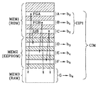
図2は、マイクロプロセッサのメモリアレイを示し、あるメモリゾーンはアプリケーションのために確保され、その他は厳しく禁じられていて斜線で示されている。この図は、プログラムPGAが記録されているゾーンA、プログラムPGBが記録されているゾーンB、プログラムPGAおよびPGBによって共用されるサブプログラムLIB (ライブラリ)が記録されているゾーンC、プログラムPGAのために読み取りおよび書き込みモードで確保されているデータゾーンD、プログラムPGBのために読み取りおよび書き込みモードで確保されているデータゾーンE、サブプログラムLIBのために読み取りおよび書き込みモードで確保されているデータゾーンF、及び3つのプログラムPGA、PGB、LIBのための読み取りおよび書き込みモードで利用可能なゾーンGを示している。ゾーンA、B、Cは、例えば、メモリMEM1(ROM)内にレイアウトされ、ゾーンD、E、FはメモリMEM2(EEPROM)内にレイアウトされ、ゾーンGはメモリMEM3(RAM)にレイアウトされる。図示されるように、メモリゾーンの識別コードCIMは、ゾーンAないしGの識別にそれぞれ割り当てられた7つのコードビットb0ないしb6からなり、プログラムゾーン識別のためのコードCIP1およびCIP2は、ビットb0、b1、およびb2からなる。
【0038】
この例では、プログラムPGAがサブプログラムに計算ステップの結果をゾーンDへ記録することを求めることができるように、またプログラムPGBがサブプログラムにこのような結果をゾーンEに記録することを求めることができるように、サブプログラムLIBは、このサブプログラムを呼び出すプログラムPGAまたはPGBの権利の恩恵を受けることが望ましく、このサブプログラムは、永続的な権利のおかげで、一時的結果の格納のためにゾーンFおよびGを使用することが出来る。
【0039】
従来の技術では、この目的を達成するために使用された解決策は、サブプログラムにゾーンDおよびEに対する永続的な権利を割り当てさせることにあったのだろうが、これはメモリアレイの区分壁を破ることを課すものであった。
【0040】
本発明によれば、マイクロプロセッサがサブプログラムを入力した場合に、ゾーンDおよびEの一方に対する権利が、呼出しプログラムの機能として、サブプログラムに一時的に割り当てられる。
【0041】
より明確なイメージを与えるために、図3は、このような一時的な権利の割り当て引き起こすために用いられるテーブルTDA1の典型的な実施形態を示している。テーブルTDA1は、3本の水平ラインLH0ないしLH2、7本の垂直ラインLV0ないしLV6、及び3本の出力ラインLS0ないしLS2を備えている。以下を容易に理解できるようにするために、実行されているプログラムの識別コードCIP1のビットをb0’ないしb2’、サブプログラムを呼び出すプログラムの識別コードCIP2のビットをb0”ないしb2”とする。
【0042】
垂直ラインLV0ないしLV6は、それぞれコードCIMのビットb0ないしb6を受け取る。ラインLH0は、ビットb0’及びb0”の論理和の結果を受け取る。ラインLH1は、ビットb1’及びb1”の論理和の結果を受け取る。ラインLH2は、ビットb2’が依然として0であるため、b2’のみを受け取る。ラインLS0ないしLS2は、それぞれ信号VLTを形成するようゲート12で結合される許可ビットa0ないしa2を出力する。
【0043】
プログラムPGA、PGB、及びサブプログラムLIBに割り当てられる、メモリアレイへの永続的アクセス権は、水平ラインLHiと垂直ラインLVjの交点に配置されたMOSトランジスタTi,jの形をとる。ラインLHi及びLVjの交点に配置されたトランジスタTi,jは、そのゲートによってラインLHiに、そのドレインによってラインLVjに、またそのソースによって出力ラインLSiに接続されている。なお、プログラムPGAの、ラインLH0と、それ自身のメモリゾーンA、サブプログラムLIBを含むゾーンC、及びゾーンD及びGに対する永続的な権利を決定するラインLV0、LV2、LV3、及びLV6との交点においてトランジスタを区別することができる(図2)。この図はまた、ラインLH1と、プログラムPGBの永続的権利を決定するラインLV1、LV2、LV4、及びLV6の交点におけるトランジスタ、及びラインLH2と、プログラムゾーンC及びゾーンFおよびGに対するサブプログラムLIBの永続的な権利を決定するラインLV2、LV5、及びLV6、の交点におけるトランジスタを示す。
【0044】
テーブルTDA1の動作は、プラグラムPGA、PGB、及びLIBに対する永続的な権利の割り当てに関しては、それ自体、標準的である。各出力ラインLS0ないしLS1は、レジスタ、それぞれr1ないしr3によって0に保持されており、そのソースによって出力ラインに接続されているトランジスタTi,jが、そのゲートにおいて1であるビットを、そのドレインにおいてシステムの電源電圧に相当する論理“1”を受け取った場合に1になる。
【0045】
サブプログラムの一時的および永続的権利の割り当ては、マイクロプロセッサがサブプログラムへ切り換えると発生する。その時点で、コードCIP1のビットb2’は1である。これは、サブプログラムの権利を活性化する。さらに、サブプログラムがプログラムPGAまたはPGBのどちらによって呼び出されたか次第で、コードCIP2のビットb0”またはb1”もまた1となる。これは、プログラムPGAまたはPGBの権利をサブプログラムの恩恵状態に保つものである。
【0046】
当然のことながら、テーブルTDA1は、当業者の範囲内である様々な代替実施形態、特に、逆の論理構成に開かれている。
【0047】
さらに、上記には呼出しプログラムの権利をサブプログラムに譲渡することが提案されているが、サブプログラムに割り当てられる一時的な権利の範囲に関しては、本発明の種々の代替実施形態が考案され得る。
【0048】
一例として、図4は、テーブルTDA1と同様の垂直ラインLV0ないしLV6を有するが、ビットb0’、b1’、b0”、及びb1”をそれぞれ、これらのビットの論理結合なしに受け取る4本の水平ラインLH0ないしLH3を有するテーブルTDA2を示す。ラインの交点におけるトランジスタT,jは、矢印によって出力ライン、この場合は4本のラインLS0ないしLS3に接続されている点によって模式的に表されている。ここでは、サブプログラムLIBに永続的権利を割り当てるための水平ラインは設けられていない。従って、この例では、これらの永続的な権利は皆無であるが、それらが皆無でないことも考えられ得るであろう。
【0049】
テーブルTDA2は、ラインLH0およびLH1がプログラムPGAおよびPGBの永続的な権利を定義し、ビットb0”及びb1”のみによって起動されるラインLH2およびLH3がサブプログラムLIBの一時的な権利を定義するという点においてテーブルTDA1と異なる。ラインLH2およびLH3は、ラインLH0 およびLH1と異なり、独立しているので、呼出しプログラムの永続的な権利とは異なる一時的な権利を呼出しプログラムの機能として、サブプログラムに割り当てることが可能である。したがって、図示された例では、トランジスタTi,jは、以下の割り当てがなされるようにレイアウトされる。
プログラムPGAに対して:それ自体のプログラムゾーンAに対する権利、サブプログラムLIBのプログラムゾーンCに対する権利、及びゾーンGに対する権利プログラムPGBに対して:それ自体のプログラムゾーンBに対する権利、サブプログラムLIBのプログラムゾーンCに対する権利、及びゾーンGに対する権利プログラムPGAによって呼び出されている時のサブプログラムLIBに対して:それ自体のプログラムゾーンCに対する権利、及びゾーンE及びGに対する権利
プログラムPGBによって呼び出されている時のサブプログラムLIBに対して:それ自体のプログラムゾーンCに対する権利、及びゾーンF及びGに対する権利
【0050】
最終に、サブプログラムへの切り換えにおいて、ラッチLT2により記録されたビットb0”及びb1”を受け取る2本の特別ラインLH2及びLH3を設けることによって、サブプログラムに対して特別な権利を割り当てることが可能である。これらの特別な権利は、呼出しプログラムによって決定され、同時に、このプログラムの権利とは独立している。
【0051】
さらに、この例では、権利の割り当ては、コードCIP2のビットb0”およびb1”のみによるので、サブプログラムLIBに割り当てられた権利は、プログラムPGA及びPGBによって呼び出され得る、任意の他のサブプログラムにも割り当てることができることが分かる。
【0052】
図5は,テーブルTDA2と同様のテーブルTDA3を示すが、ここでは、ラインLH2は、ANDゲートによってビットb2’と結合されたビットb0”を受け取り、LH3は、別のANDゲートによってビットb2’と結合されたビットb1”を受け取る。この場合、ラインLH2またはLH3は、ビットb2’が1に等しく、ビットb0”またはb1”もまた1であるという2重条件でのみ起動され得る。こうして、権利の一時的な譲渡は、任意の他のサブプログラムを除外して、サブプログラムLIBに対して確保される。
【0053】
本発明はもちろん、呼出しプログラムの本質の格納によるサブプログラムへの一時的な権利の譲渡の、本発明による原理に基づいた、変形例および代替実施形態に対して開かれている。特に、それら自体メインプログラムによって呼び出される1次レベルのサブプログラムによって呼び出された2次レベルのサブプログラムに対して、カスケード式の権利の譲渡が考案されることができる。
【0054】
最後に、上でさらに説明された権利割り当てテーブルの実施形態は、本発明の理解を容易にする目的で、トランジスタを用いたマトリクス回路の形式で示されているが、本発明による権利割り当てテーブルは、実際にはいくつかの他の形式を想定することが可能であることに留意しなければならない。特に、この種のテーブルは、VHDL言語コンパイラによって自動的に作成されるブール論理回路の形式で作ることができる。このハイレベルな言語で書かれた機能からの論理回路の自動的な作成方法は、近年、大きな発展を遂げた。
【図面の簡単な説明】
【図1】本発明にかかる権利管理システムを備えたマイクロプロセッサを示すブロック図である。
【図2】マイクロプロセッサのメモリアレイを示し、本発明にかかる権利管理システムの一実施例を図示する。
【図3】図2に示した実施例に関する権利割り当てテーブルの典型的な実施形態を示す。
【図4】本発明にかかる権利割り当てテーブルの他の典型的な実施形態の概略図である。
【図5】本発明にかかる権利割り当てテーブルの他の典型的な実施形態の概略図である。
【符号の説明】
1 アドレスバス
2 データバス
10 権利割り当てシステム
11 ORゲート
12 ゲート
LT1 ラッチ
LT2 第2のラッチ[0001]
BACKGROUND OF THE INVENTION
The present invention relates to microprocessors, and more particularly to protected microprocessors.
[0002]
Protected microprocessors are most commonly used in applications where access to certain sensitive data or programs needs to be prohibited. Thus, in order to protect a memory zone with a secret code or ciphertext algorithm, for example, a smart card is typically provided in a protected microprocessor.
[0003]
[Prior art]
Traditionally, microprocessors are protected by an address control system that verifies that the program being executed is entitled to address a memory zone for read, write, jump, or call operations. Yes. This type of system is generally a rights assignment table that receives the identification code of the program being executed at the first input and receives the identification code of the addressed memory zone at the second input. . The memory zone corresponds to the current address present on the microprocessor address bus. In the table, if the program being executed is scheduled to be able to use the addressed memory zone, the table outputs a permission signal. Otherwise, the table does not output a permission signal and an address violation signal is transmitted.
[0004]
This type of address control system is used to obtain protected coexistence of various programs in a microprocessor memory array by assigning different rights to each of those programs. These various programs typically correspond to different microprocessor applications planned by the manufacturer.
[0005]
[Problems to be solved by the invention]
However, the protection of the microprocessor is negative to the configuration of the memory array in that it divides the memory array into various mutually “sealed” parts, each part reserved for one application. affect. Currently, programs designed for different applications often have similar calculation steps that can be centralized in a common area as a “library”. A library, in terms of those skilled in the art, refers to one or more subprograms shared by several programs.
[0006]
The standard method of centralizing program parts of a library format common to some programs is generally prohibited for protected microprocessors because of the safety issues it causes. For example, assume that program PGA enjoys the right to access zone “X” of the memory array, and program PGB enjoys the right to access zone “Y” different from “X”. Designing a subprogram shared by program PGA and program PGB causes the problem of finding which is the right to be given to the subprogram. The subprogram must be able to read and write data in zone “X” when called by program PGA, and can read and write data in zone “Y” when called by program PGB If so, the subprogram must be granted the combined rights of programs PGA and PGB, ie, the rights to zone “X” and zone “Y”. However, the program PGB, or a malicious program loaded in the location of the program PGB, may be able to use the subprogram to access the zone “X” reserved for the program PGA and vice versa. The same is true. Therefore, designing a subprogram that is shared by two programs with different access rights to the memory array is a violation in the partitioning of the memory array.
[0007]
The present invention seeks to overcome this drawback.
[0008]
In particular, the present invention seeks to provide a means for providing subprograms shared by several programs without compromising the integrity of the rights granted to each of the programs.
[0009]
[Means for Solving the Problems]
This object is achieved by designing a protected microprocessor with a rights assignment system for assigning permanent access to a zone of the microprocessor memory array to a program executable by the microprocessor. And the rights assignment system provides a means for providing temporary access to a memory zone to a subprogram shared by at least two programs when the subprogram is called by one of the programs The temporary right range is a function of a program calling a subprogram.
[0010]
According to an embodiment, the rights assignment system comprises means for temporarily granting the rights of the calling program to the subprogram.
[0011]
According to an embodiment, the rights assignment system further comprises means for further granting the subprogram permanent rights independent of the calling program.
[0012]
According to one embodiment, the rights assignment system includes a program or subprogram identification code at a first input and a memory zone specified by a current address flowing through a microprocessor address bus at a second input. A right assignment table laid out for receiving the identification code; and means for inputting the identification code of the program that called the subprogram to the first input of the right assignment table during execution of the subprogram.
[0013]
According to an embodiment, during execution of a subprogram, the rights assignment system includes an identification code of a subprogram being executed and a program that called the subprogram as a first input of a rights assignment table. Means for simultaneously inputting the identification code.
[0014]
According to an embodiment, the identification code bit of the subprogram being executed and the identification code bit of the program that called the subprogram are logically input before being input to the first input of the rights assignment table. Combined by function.
[0015]
According to one embodiment, the rights assignment system includes a first latch for storing an identification code of a program or subprogram being executed during execution of an instruction, the input of which is the first latch. A second latch connected to the output and laid out to store the identification code of the program being executed when the microprocessor switches to the subprogram and forming the identification code of the program that called the subprogram. The second latch is reset when the microprocessor finishes the subprogram.
[0016]
According to an embodiment, the loading and resetting of the second latch receives the current address flowing through the address bus at the input, and detects the loading signal when the address of the first instruction of the subprogram is detected. When the address of the last instruction of the subprogram is detected and is laid out to be input to the second latch, it is controlled by an address decoder that transmits a reset signal to the second latch.
[0017]
According to one embodiment, an identification code of a memory zone specified by a current address and an identification code of a program and subprogram being executed are address decoders that receive the current address flowing through the address bus at the input. Sent by.
[0018]
According to an embodiment, the rights distribution system sends a violation signal if an address present on the address bus does not correspond to a right permanently or temporarily assigned to the program or subprogram being executed. .
[0019]
According to one embodiment, the violation signal is processed by an interrupt decoder to send the microprocessor to an address violation processing subprogram.
[0020]
DETAILED DESCRIPTION OF THE INVENTION
These and other objects, features and advantages of the present invention will be given as a non-limiting description of an exemplary embodiment of a microprocessor according to the present invention and in the following description made with reference to the accompanying drawings, Further details will be described.
[0021]
FIG. 1 is a block diagram of a microprocessor MP that includes a read only memory MEM1 (ROM), an electrically erasable programmable memory MEM2 (EEPROM), and a random access memory MEM3 (RAM). These various memories are connected to the microprocessor by an address bus 1 and a data bus 2, and together form a memory array of the microprocessor.
[0022]
According to the present invention, the microprocessor MP includes a
[0023]
The
CIM = b0 b1 ... bn bn + 1 ... bm
Here, each bit is assigned to the identification of a predetermined memory zone, and only one bit can be 1 at a time and the others are 0.
[0024]
In the following, it is assumed that bits b0 to bn are assigned to specify a memory zone made of memory, and bits bn + 1 to bm are assigned to specify a memory zone made of data. For example, the memory zone is arranged in the memory MEM1, and the data zone is arranged in the memories MEM2 and MEM3.
[0025]
Bits b0 to bn of the code CIM are input to an input of a latch LT1 driven by a loading signal LOAD1 output from the microprocessor MP. When signal LOAD1 is input to latch LT1, the output of the latch duplicates the input of the latch and outputs code CIP1 for program zone identification.
[0026]
The code CIP1 is input to the input of the second latch LT2 driven by the loading signal LOAD2 and the reset signal RST output from the decoder DEC2. When the signal LOAD2 is input to the latch LT2, the output of the latch LT2 outputs a code CIP2 that duplicates the code CIP1 at the input.
[0027]
The codes CIP1 and CIP2 are combined to form a code CIP3, which is input to the input E1 of the right assignment table TDA that receives the code CIM output from the decoder DEC1 at the input E2. In this embodiment, the combination of the codes CIP1 and CIP2 is provided by the
[0028]
Rights assignment table TDA, basic output S 0 ~ S n Each output S 0 ~ S n Is the basic input E1 of the input E1 that receives one of the bits of the code CIP3 1 ,…, E1n of the same order. Output S 0 ~ S n The permission bit a 0 ~ A n The access right is output in the form of Permission bit a i Is the corresponding input E1 i Bit b is equal to 1 bit i Is equal to 1 bit and bit b i And allowed combinations that are 1 bit {b i , b j } Is formed. Allowed combinations {b i , b j } Will eventually be recorded on the table, defining permanent rights.
[0029]
The loading signal LOAD1 of the latch LT1 is transmitted from the microprocessor MP when the microprocessor MP reads an instruction in the memory MEM1 or is about to read (microprocessor read cycle or fetch cycle). At that time, the address ADR present on the address bus is the address IADR of the instruction transmitted from the microprocessor order counter PC. Therefore, the code CIM transmitted from the decoder DEC1 is a bit b that designates a memory zone having this instruction. i 1 to have. This bit b i Is found at the code CIP1 recorded in the latch LT1 and at the input E1 of the table TDA.
[0030]
Further, the signal LOAD2 is transmitted from the decoder DEC2 when the decoder DEC2 detects the address ADRin of the first instruction of the shared subprogram on the bus 1, and the signal RST is transmitted from the decoder DEC2 to the address of the last instruction of the shared subprogram. When ADRout is detected on the address bus, it is transmitted from the decoder DEC2. Addresses ADRin and ADRout are preset and represent the input address and output address of the subprogram being considered. When several subprograms are shared by multiple programs, the decoder DEC2 detects the input address and output address of each subprogram, and sends a signal LOAD2 or signal RST when one of these addresses is detected To be laid out.
[0031]
The
[0032]
The operation of the
[0033]
Since the codes CIP1 and CIP2 are now combined in the
[0034]
The
[0035]
In practice, the signal VLT transmitted when a permanent or temporary rights violation occurs may be used in different ways to prevent access to a prohibited memory zone. As shown in FIG. 1, the signal VLT is input to, for example, the input of the interrupt decoder ITDEC, and the output transmits the address ITADR of the subprogram that handles the address violation case. The address ITADR is input to the input of the multiplexer MUX that receives the address IADR of the next instruction transmitted from the rank counter PC at another input. The multiplexing device is driven by the signal IT transmitted from the decoder ITDEC, and when the signal IT is transmitted, transmits the address ITADR instead of the address IADR to the address bus. In one alternative embodiment, the signal VLT is used to set the microprocessor reset signal (RESET) to 0 to deactivate the microprocessor. In another alternative embodiment, signal VLT is used to generate a non-maskable interrupt.
[0036]
The operation of the
[0037]
FIG. 2 shows a microprocessor memory array, where certain memory zones are reserved for applications and others are strictly forbidden and shown with diagonal lines. This figure is for zone A in which program PGA is recorded, zone B in which program PGB is recorded, zone C in which subprogram LIB (library) shared by programs PGA and PGB is recorded, and program PGA Data zone D reserved in read and write mode, data zone E reserved in read and write mode for program PGB, data zone F reserved in read and write mode for subprogram LIB And zone G available in read and write mode for three programs PGA, PGB and LIB. Zones A, B, and C are, for example, laid out in the memory MEM1 (ROM), zones D, E, and F are laid out in the memory MEM2 (EEPROM), and zone G is laid out in the memory MEM3 (RAM). As shown in the figure, the identification code CIM of the memory zone is composed of seven code bits b0 to b6 respectively assigned to the identification of zones A to G, and the codes CIP1 and CIP2 for identifying the program zone are bits b0, It consists of b1 and b2.
[0038]
In this example, so that the program PGA can ask the subprogram to record the result of the calculation step in zone D, and the program PGB asks the subprogram to record such a result in zone E. The subprogram LIB should benefit from the rights of the program PGA or PGB that calls this subprogram so that this subprogram can store temporary results thanks to the permanent right Zones F and G can be used.
[0039]
In the prior art, the solution used to achieve this goal would have been to allow subprograms to assign permanent rights to zones D and E, which is the partition wall of the memory array. To impose a break.
[0040]
According to the present invention, when the microprocessor inputs a subprogram, the right to one of zones D and E is temporarily assigned to the subprogram as a function of the calling program.
[0041]
In order to give a clearer picture, FIG. 3 shows an exemplary embodiment of the table TDA1 used to cause such a temporary rights assignment. The table TDA1 includes three horizontal lines LH0 to LH2, seven vertical lines LV0 to LV6, and three output lines LS0 to LS2. In order to easily understand the following, the bits of the identification code CIP1 of the program being executed are b0 'to b2', and the bits of the identification code CIP2 of the program calling the subprogram are b0 "to b2".
[0042]
The vertical lines LV0 to LV6 receive bits b0 to b6 of the code CIM, respectively. Line LH0 receives the logical OR result of bits b0 ′ and b0 ″. Line LH1 receives the logical OR result of bits b1 ′ and b1 ″. Line LH2 receives only b2 'because bit b2' is still zero. Lines LS0 to LS2 output permission bits a0 to a2 that are coupled at
[0043]
The permanent access right to the memory array assigned to the programs PGA, PGB, and subprogram LIB takes the form of MOS transistors Ti, j arranged at the intersections of the horizontal line LHi and the vertical line LVj. The transistor Ti, j disposed at the intersection of the lines LHi and LVj is connected to the line LHi by its gate, to the line LVj by its drain, and to the output line LSi by its source. The intersection of line LH0 of program PGA with lines LV0, LV2, LV3, and LV6 that determine permanent rights to its own memory zone A, zone C including subprogram LIB, and zones D and G In FIG. 2, the transistors can be distinguished. This figure also shows the transistors at the intersection of line LH1 and lines LV1, LV2, LV4, and LV6 that determine the permanent right of program PGB, and subprogram LIB for program zone C and zones F and G. The transistors at the intersections of lines LV2, LV5, and LV6 that determine permanent rights are shown.
[0044]
The behavior of table TDA1 is as follows for the permanent assignment of rights to the programs PGA, PGB and LIB: As such Standard. Each output line LS0 to LS1 is held at 0 by a register, r1 to r3, respectively, and the transistor Ti, j connected to the output line by its source has a bit at its drain that is 1 at its gate. It becomes 1 when a logic “1” corresponding to the power supply voltage of the system is received.
[0045]
Subprogram temporary and permanent rights assignment occurs when the microprocessor switches to a subprogram. At that time, the bit b2 ′ of the code CIP1 is “1”. This activates the rights of the subprogram. Furthermore, depending on whether the subprogram is called by the program PGA or PGB, the bits b0 "or b1" of the code CIP2 are also set to 1. This keeps the rights of the program PGA or PGB in the subprogram benefit state.
[0046]
Of course, the table TDA1 is open to various alternative embodiments that are within the purview of those skilled in the art, and in particular, to the reverse logical configuration.
[0047]
Furthermore, although it has been proposed above to transfer the rights of the calling program to the subprogram, various alternative embodiments of the present invention can be devised with respect to the range of temporary rights assigned to the subprogram.
[0048]
As an example, FIG. 4 has vertical lines LV0 to LV6 similar to table TDA1, but four horizontal lines that receive bits b0 ′, b1 ′, b0 ″, and b1 ″, respectively, without logical combination of these bits. A table TDA2 having lines LH0 to LH3 is shown. The transistors T, j at the intersections of the lines are schematically represented by the points connected to the output line, in this case the four lines LS0 to LS3, by arrows. Here, there is no horizontal line for assigning permanent rights to the subprogram LIB. Thus, in this example, these permanent rights are none, but it could be considered that they are not.
[0049]
Table TDA2 states that lines LH0 and LH1 define the permanent rights of programs PGA and PGB, and lines LH2 and LH3 activated only by bits b0 ”and b1” define the temporary rights of subprogram LIB This differs from the table TDA1. Since the lines LH2 and LH3 are independent of the lines LH0 and LH1, the temporary rights different from the permanent rights of the calling program can be assigned to the subprogram as a function of the calling program. Accordingly, in the illustrated example, the transistors Ti, j are laid out so that the following assignments are made.
For program PGA: right for its own program zone A, right for program zone C of subprogram LIB, and right for zone G For program PGB: right for its own program zone B, program for subprogram LIB Rights to Zone C and Rights to Zone G For subprogram LIB when invoked by program PGA: Rights to its own program zone C and rights to zones E and G
For subprogram LIB when called by program PGB: rights to its own program zone C, and rights to zones F and G
[0050]
Finally, when switching to a subprogram, special rights can be assigned to the subprogram by providing two special lines LH2 and LH3 that receive the bits b0 "and b1" recorded by the latch LT2. It is. These special rights are determined by the calling program and at the same time are independent of the rights of this program.
[0051]
Furthermore, in this example, the assignment of rights is only by bits b0 "and b1" of code CIP2, so the rights assigned to subprogram LIB can be transferred to any other subprogram that can be called by programs PGA and PGB. Can also be assigned.
[0052]
FIG. 5 shows a table TDA3 similar to table TDA2, but here line LH2 receives bit b0 "combined with bit b2 'by an AND gate, and LH3 receives bit b2' by another AND gate. Receive the combined bit b1 ". In this case, the line LH2 or LH3 can only be activated under the double condition that the bit b2 ′ is equal to 1 and the bit b0 ″ or b1 ″ is also 1. Thus, temporary transfer of rights is reserved for the subprogram LIB, excluding any other subprograms.
[0053]
The invention is of course open to variants and alternative embodiments based on the principle according to the invention of the temporary transfer of rights to subprograms by storing the nature of the calling program. In particular, cascading rights assignments can be devised for secondary level subprograms that are called by primary level subprograms that are themselves called by the main program.
[0054]
Finally, the embodiment of the rights assignment table further described above is shown in the form of a matrix circuit using transistors for the purpose of facilitating the understanding of the invention. It should be noted that in practice it is possible to assume several other forms. In particular, this type of table can be created in the form of a Boolean logic circuit automatically created by a VHDL language compiler. In recent years, a method for automatically creating a logic circuit from functions written in this high-level language has been greatly developed.
[Brief description of the drawings]
FIG. 1 is a block diagram showing a microprocessor including a rights management system according to the present invention.
FIG. 2 illustrates a microprocessor memory array and illustrates one embodiment of a rights management system according to the present invention.
3 illustrates an exemplary embodiment of a rights assignment table for the example shown in FIG.
FIG. 4 is a schematic diagram of another exemplary embodiment of a rights assignment table according to the present invention.
FIG. 5 is a schematic diagram of another exemplary embodiment of a rights assignment table according to the present invention.
[Explanation of symbols]
1 Address bus
2 Data bus
10 Rights assignment system
11 OR gate
12 Gate
LT1 latch
LT2 second latch
Claims (10)
ことを特徴とする保護されたマイクロプロセッサ。A rights assignment system for assigning a program executable by a microprocessor with permanent access to a zone of a microprocessor memory array, the system having a program or subprogram identification code at a first input In a protected microprocessor comprising a rights assignment table that receives an identification code of a memory zone specified by a current address flowing in an address bus at a second input, the system being shared by at least two programs that the sub-program, if the sub-program is called by one of the program is arranged to provide temporary access to certain memory zones, for this purpose, subprogram fruit During, the first input of the rights allocation table, comprising means for inputting an identification code of the program that called the subprogram,
A protected microprocessor, characterized in that.
前記権利割り当てシステムは、サブプログラムに対して呼出しプログラムの権利を一時的に与える手段を備える、
ことを特徴とするマイクロプロセッサ。The microprocessor of claim 1, wherein
The rights assignment system comprises means for temporarily granting the rights of a calling program to a subprogram.
A microprocessor characterized by that.
前記権利割り当てシステムは、サブプログラムに対して、呼出しプログラムとは独立した永続的な権利をさらに与える手段を備える、
ことを特徴とするマイクロプロセッサ。The microprocessor according to claim 1 or 2,
The rights assignment system further comprises means for giving the subprogram a permanent right independent of the calling program.
A microprocessor characterized by that.
前記権利割り当てシステムは、サブプログラムの実行中に、前記権利割り当てテーブルの第1の入力に、実行されている前記サブプログラムの識別コードと、前記サブプログラムを呼び出したプログラムの識別コードとを、同時に入力する手段を備えた、
ことを特徴とするマイクロプロセッサ。The microprocessor according to any one of claims 1 to 3,
During execution of the subprogram , the right assignment system simultaneously receives the identification code of the subprogram being executed and the identification code of the program that called the subprogram at the first input of the right assignment table. With means to input,
A microprocessor characterized by that.
実行されている前記サブプログラムの識別コードのビットと、前記サブプログラムを呼び出したプログラムの識別コードのビットが、前記権利割り当てテーブルの第1の入力に入力される前に論理機能によって結合される、
ことを特徴とするマイクロプロセッサ。The microprocessor according to any one of claims 1 to 4 ,
The identification code bit of the subprogram being executed and the identification code bit of the program that called the subprogram are combined by a logic function before being input to the first input of the rights assignment table;
A microprocessor characterized by that.
前記権利割り当てシステムは、
命令の実行中に、実行されている前記プログラムまたはサブプログラムの識別コードを格納するための第1のラッチと、
その入力が前記第1のラッチの出力に接続され、マイクロプロセッサがサブプログラムに切り換える時に実行されているプログラムの識別コードを格納するようにレイアウトされて、このサブプログラムを呼び出したプログラムの識別コードを形成するものであって、マイクロプロセッサが前記サブプログラムを終了するとリセットされる第2のラッチとを備える、
ことを特徴とするマイクロプロセッサ。The microprocessor according to any one of claims 1 to 5 ,
The rights assignment system includes:
A first latch for storing an identification code of the program or subprogram being executed during execution of the instruction;
The input is connected to the output of the first latch and is laid out to store the identification code of the program being executed when the microprocessor switches to the subprogram. And a second latch that is reset when the microprocessor exits the subprogram,
A microprocessor characterized by that.
前記第2のラッチのローディング及びリセットは、アドレスバスを流れる現在のアドレスを入力において受信し、サブプログラムの第1の命令のアドレスが検出されると、ローディング信号を前記第2のラッチに入力するようにレイアウトされ、リセット信号を前記第2のラッチに送信する、アドレスデコーダによって制御される、
ことを特徴とするマイクロプロセッサ。The microprocessor of claim 6 , wherein
The loading and reset of the second latch receives the current address flowing through the address bus at the input, and inputs the loading signal to the second latch when the address of the first instruction of the subprogram is detected. , And controlled by an address decoder that sends a reset signal to the second latch,
A microprocessor characterized by that.
現在のアドレスによって指定されるメモリゾーンの識別コードと、実行されているプログラムおよびサブプログラムの識別コードとは、アドレスバスを流れる現在のアドレスを入力において受信するアドレスデコーダによって送信される、ことを特徴とするマイクロプロセッサ。The microprocessor according to any one of claims 1 to 7 ,
The identification code of the memory zone specified by the current address and the identification code of the program and subprogram being executed are transmitted by an address decoder that receives at its input the current address flowing through the address bus. And a microprocessor.
前記権利割り当てシステムは、前記アドレスバスに存在するアドレスが、実行されているプログラムまたはサブプログラムに永続的にあるいは一時的に割り当てられる権利に対応しない場合、違反信号を送信する、
ことを特徴とするマイクロプロセッサ。The microprocessor according to any one of claims 1 to 8,
The rights assignment system transmits a violation signal if an address present on the address bus does not correspond to a right permanently or temporarily assigned to the program or subprogram being executed;
A microprocessor characterized by that.
前記アドレス違反信号は、割り込みデコーダによって処理されて、マイクロプロセッサをアドレス違反処理サブプログラムに送る、
ことを特徴とするマイクロプロセッサ。The microprocessor of claim 9 , wherein
The address violation signal is processed by an interrupt decoder to send the microprocessor to an address violation processing subprogram;
A microprocessor characterized by that.
Applications Claiming Priority (1)
| Application Number | Priority Date | Filing Date | Title |
|---|---|---|---|
| FR0008283A FR2811096A1 (en) | 2000-06-28 | 2000-06-28 | SECURE MICROPROCESSOR INCLUDING A SYSTEM FOR ALLOCATING RIGHTS TO LIBRARIES |
Publications (2)
| Publication Number | Publication Date |
|---|---|
| JP2005037974A JP2005037974A (en) | 2005-02-10 |
| JP3661852B2 true JP3661852B2 (en) | 2005-06-22 |
Family
ID=8851778
Family Applications (1)
| Application Number | Title | Priority Date | Filing Date |
|---|---|---|---|
| JP2001195422A Expired - Fee Related JP3661852B2 (en) | 2000-06-28 | 2001-06-27 | Protected microprocessor with system for assigning rights to the library |
Country Status (4)
| Country | Link |
|---|---|
| US (1) | US6925569B2 (en) |
| EP (1) | EP1168184A1 (en) |
| JP (1) | JP3661852B2 (en) |
| FR (1) | FR2811096A1 (en) |
Families Citing this family (10)
| Publication number | Priority date | Publication date | Assignee | Title |
|---|---|---|---|---|
| FR2833374A1 (en) * | 2001-12-12 | 2003-06-13 | Cp8 | METHOD AND DEVICE FOR CONTROLLING ACCESS IN AN ONBOARD SYSTEM |
| KR100505106B1 (en) * | 2002-05-29 | 2005-07-29 | 삼성전자주식회사 | Smart card with enhanced security |
| JP4115759B2 (en) * | 2002-07-01 | 2008-07-09 | 株式会社東芝 | Method and program for using shared library in tamper resistant processor |
| EP1507185A1 (en) * | 2003-08-11 | 2005-02-16 | Axalto S.A. | Method and device for protecting against unauthorized access to a secure routine |
| US7797728B2 (en) * | 2004-10-27 | 2010-09-14 | Intel Corporation | Mechanism to generate restricted and unrestricted execution environments |
| NO20050564D0 (en) * | 2005-02-02 | 2005-02-02 | Tore Lysemose Hansen | Program monitor to identify unauthorized intrusion into computer systems |
| ITTO20070229A1 (en) * | 2007-03-30 | 2008-09-30 | Faiveley Transport Italia Spa | METHOD FOR THE PROTECTION OF PHYSICAL MEMORY IN A MICROPROCESSOR SYSTEM |
| DE102013226872A1 (en) * | 2013-10-15 | 2015-04-16 | Continental Automotive Gmbh | Method for operating a control unit of a motor vehicle and control unit for a motor vehicle |
| JP6493672B2 (en) * | 2015-04-16 | 2019-04-03 | 大日本印刷株式会社 | Electronic information storage medium, abnormality detection method, abnormality detection program, and IC card |
| GB2569358B (en) | 2017-12-15 | 2020-01-29 | Advanced Risc Mach Ltd | Code realms |
Family Cites Families (9)
| Publication number | Priority date | Publication date | Assignee | Title |
|---|---|---|---|---|
| JPS5140772B2 (en) * | 1971-07-26 | 1976-11-05 | ||
| US4442484A (en) * | 1980-10-14 | 1984-04-10 | Intel Corporation | Microprocessor memory management and protection mechanism |
| EP0432359A3 (en) * | 1989-11-21 | 1993-03-17 | International Business Machines Corporation | Method and apparatus for performing memory protection operations in a parallel processor system |
| FR2683357A1 (en) * | 1991-10-30 | 1993-05-07 | Philips Composants | MICROCIRCUIT FOR PROTECTED PROGRAMMABLE MEMORY CHIP CARD. |
| JP2757777B2 (en) * | 1994-05-26 | 1998-05-25 | 住友金属工業株式会社 | Method and system for detecting unauthorized access to memory |
| US5551051A (en) * | 1994-09-20 | 1996-08-27 | Motorola, Inc. | Isolated multiprocessing system having tracking circuit for verifyng only that the processor is executing set of entry instructions upon initiation of the system controller program |
| JP3713141B2 (en) * | 1998-05-19 | 2005-11-02 | インターナショナル・ビジネス・マシーンズ・コーポレーション | How to prevent unauthorized execution of programs |
| US6757802B2 (en) * | 2001-04-03 | 2004-06-29 | P-Cube Ltd. | Method for memory heap and buddy system management for service aware networks |
| US6820177B2 (en) * | 2002-06-12 | 2004-11-16 | Intel Corporation | Protected configuration space in a protected environment |
-
2000
- 2000-06-28 FR FR0008283A patent/FR2811096A1/en not_active Withdrawn
-
2001
- 2001-05-28 EP EP01112777A patent/EP1168184A1/en not_active Withdrawn
- 2001-06-20 US US09/885,450 patent/US6925569B2/en not_active Expired - Lifetime
- 2001-06-27 JP JP2001195422A patent/JP3661852B2/en not_active Expired - Fee Related
Also Published As
| Publication number | Publication date |
|---|---|
| JP2005037974A (en) | 2005-02-10 |
| US20020016890A1 (en) | 2002-02-07 |
| US6925569B2 (en) | 2005-08-02 |
| EP1168184A1 (en) | 2002-01-02 |
| FR2811096A1 (en) | 2002-01-04 |
Similar Documents
| Publication | Publication Date | Title |
|---|---|---|
| CN100371906C (en) | Method and apparatus for determining access permission | |
| US5432950A (en) | System for securing a data processing system and method of operation | |
| US5704039A (en) | Mask programmable security system for a data processor and method therefor | |
| EP0851358B1 (en) | Processing system security | |
| US8189384B2 (en) | System and method to control one time programmable memory | |
| US20040177266A1 (en) | Data processing system with peripheral access protection and method therefor | |
| US9619405B2 (en) | Device having memory access protection | |
| EP0443557B1 (en) | Interrupt controller capable of realizing interrupt nesting function | |
| JP3661852B2 (en) | Protected microprocessor with system for assigning rights to the library | |
| US11714647B2 (en) | Resource allocation in a multi-processor system | |
| EP1483648A1 (en) | Data processing system with peripheral access protection and method therefor | |
| US20210117579A1 (en) | Secure-aware bus system | |
| US5894562A (en) | Method and apparatus for controlling bus arbitration in a data processing system | |
| US7054121B2 (en) | Protection circuit for preventing unauthorized access to the memory device of a processor | |
| KR100731527B1 (en) | Method and apparatus for overlaying memory in a data processing system | |
| JP3072706B2 (en) | Data protection device and computer system | |
| US6535943B1 (en) | Information processing device enabling floating interrupt to be pending and a method executing an interrupt condition change instruction | |
| JPS6362778B2 (en) | ||
| US7120760B2 (en) | Harvard architecture microprocessor having a linear addressable space | |
| US11604739B2 (en) | Conditional direct memory access channel activation | |
| US5799160A (en) | Circuit and method for controlling bus arbitration | |
| JPH1153338A (en) | Semiconductor integrated circuit and external bus mode selection method therefor | |
| JPH0467226B2 (en) | ||
| JPS62274445A (en) | Privilege protection system in microcomputer system | |
| JPH01261760A (en) | Computer system |
Legal Events
| Date | Code | Title | Description |
|---|---|---|---|
| TRDD | Decision of grant or rejection written | ||
| A01 | Written decision to grant a patent or to grant a registration (utility model) |
Free format text: JAPANESE INTERMEDIATE CODE: A01 Effective date: 20050301 |
|
| A61 | First payment of annual fees (during grant procedure) |
Free format text: JAPANESE INTERMEDIATE CODE: A61 Effective date: 20050316 |
|
| R150 | Certificate of patent or registration of utility model |
Free format text: JAPANESE INTERMEDIATE CODE: R150 |
|
| FPAY | Renewal fee payment (event date is renewal date of database) |
Free format text: PAYMENT UNTIL: 20090401 Year of fee payment: 4 |
|
| FPAY | Renewal fee payment (event date is renewal date of database) |
Free format text: PAYMENT UNTIL: 20100401 Year of fee payment: 5 |
|
| FPAY | Renewal fee payment (event date is renewal date of database) |
Free format text: PAYMENT UNTIL: 20110401 Year of fee payment: 6 |
|
| FPAY | Renewal fee payment (event date is renewal date of database) |
Free format text: PAYMENT UNTIL: 20120401 Year of fee payment: 7 |
|
| FPAY | Renewal fee payment (event date is renewal date of database) |
Free format text: PAYMENT UNTIL: 20130401 Year of fee payment: 8 |
|
| LAPS | Cancellation because of no payment of annual fees |