JP3660119B2 - Semiconductor dynamic quantity sensor - Google Patents
Semiconductor dynamic quantity sensor Download PDFInfo
- Publication number
- JP3660119B2 JP3660119B2 JP3632598A JP3632598A JP3660119B2 JP 3660119 B2 JP3660119 B2 JP 3660119B2 JP 3632598 A JP3632598 A JP 3632598A JP 3632598 A JP3632598 A JP 3632598A JP 3660119 B2 JP3660119 B2 JP 3660119B2
- Authority
- JP
- Japan
- Prior art keywords
- movable
- portions
- electrode
- substrate
- fixed
- Prior art date
- Legal status (The legal status is an assumption and is not a legal conclusion. Google has not performed a legal analysis and makes no representation as to the accuracy of the status listed.)
- Expired - Lifetime
Links
Images


Classifications
-
- G—PHYSICS
- G01—MEASURING; TESTING
- G01P—MEASURING LINEAR OR ANGULAR SPEED, ACCELERATION, DECELERATION, OR SHOCK; INDICATING PRESENCE, ABSENCE, OR DIRECTION, OF MOVEMENT
- G01P15/00—Measuring acceleration; Measuring deceleration; Measuring shock, i.e. sudden change of acceleration
- G01P15/02—Measuring acceleration; Measuring deceleration; Measuring shock, i.e. sudden change of acceleration by making use of inertia forces using solid seismic masses
- G01P15/08—Measuring acceleration; Measuring deceleration; Measuring shock, i.e. sudden change of acceleration by making use of inertia forces using solid seismic masses with conversion into electric or magnetic values
- G01P2015/0805—Measuring acceleration; Measuring deceleration; Measuring shock, i.e. sudden change of acceleration by making use of inertia forces using solid seismic masses with conversion into electric or magnetic values being provided with a particular type of spring-mass-system for defining the displacement of a seismic mass due to an external acceleration
- G01P2015/0808—Measuring acceleration; Measuring deceleration; Measuring shock, i.e. sudden change of acceleration by making use of inertia forces using solid seismic masses with conversion into electric or magnetic values being provided with a particular type of spring-mass-system for defining the displacement of a seismic mass due to an external acceleration for defining in-plane movement of the mass, i.e. movement of the mass in the plane of the substrate
- G01P2015/0811—Measuring acceleration; Measuring deceleration; Measuring shock, i.e. sudden change of acceleration by making use of inertia forces using solid seismic masses with conversion into electric or magnetic values being provided with a particular type of spring-mass-system for defining the displacement of a seismic mass due to an external acceleration for defining in-plane movement of the mass, i.e. movement of the mass in the plane of the substrate for one single degree of freedom of movement of the mass
- G01P2015/0814—Measuring acceleration; Measuring deceleration; Measuring shock, i.e. sudden change of acceleration by making use of inertia forces using solid seismic masses with conversion into electric or magnetic values being provided with a particular type of spring-mass-system for defining the displacement of a seismic mass due to an external acceleration for defining in-plane movement of the mass, i.e. movement of the mass in the plane of the substrate for one single degree of freedom of movement of the mass for translational movement of the mass, e.g. shuttle type
Description
【0001】
【発明の属する技術分野】
本発明は、梁構造の可動部を有し、例えば加速度、ヨーレート、振動等の力学量を検出する半導体力学量センサに関する。
【0002】
【従来の技術】
可動電極と固定電極との容量変化によって加速度等の検出を行う差動容量型半導体力学量センサでは、可動電極及び固定電極をエッチング形成した後の乾燥工程において、可動電極と固定電極との間に介在する純水の表面張力によって、可動電極及びこれに対向する固定電極が付着したり、梁とこれに対向する基板が同様に付着したりすることが問題となっている。また、上記乾燥工程以外の時、例えば梁のバネ定数により決定される力よりも大きな加速度が発生した場合にも、可動電極が固定電極に引き寄せられ、加速度が小さくなったのちにもファンデルワールス力により、可動電極と固定電極とが付着してしまうという問題がある。
【0003】
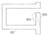
このような問題を解決するものとして、米国特許第5,542,295号明細書に示されるセンサがある。このセンサでは、図16に示すように折り曲げ梁タイプのものにおいて、梁部201から錘部202の方向に突出するストッパー部203を設け、さらに梁部201と錘部202との間隔を可動電極と固定電極との間隔よりも小さくすることで、可動電極と固定電極との付着を防止するようにしている。
【0004】
【発明が解決しようとする課題】
しかしながら、上記米国特許第5,542,295号明細書に示されるセンサにおいては、折り曲げ梁タイプのものを用いることから、梁部201の変位に伴いストッパー部が図17の点線部に示すように変位して、梁部201と錘部202との間隔を大きくし、可動電極と固定電極との間隔以上に可動部が変位できるようになってしまって付着防止ができなくなるという問題がある。差動容量型半導体力学量センサのように可動電極と固定電極との間隔が非常に狭く、この間隔と梁と錘との間隔とにあまり差を設けられないものにおいては、この問題が顕著に発生し、特に共振状態のように梁部201が基板面方向のみならず基板面垂直方向にも変位するような場合に発生し易くなる。
【0005】
本発明は上記問題に鑑みてなされ、共振状態のように梁が様々な方向に変位するような場合にも可動電極と固定電極とが付着しない半導体力学量検出センサを提供することを目的とする。
【0006】
【課題を解決するための手段】
本発明は上記目的を達成するため、以下の技術的手段を採用する。請求項1に記載の発明においては、基板(1)上に可動部(2A)と固定部(2B)とを備えてなり、前記可動部は、前記基板上に形成された第1のアンカー部(3a、3b)と、可動電極(7a、7b、8a、8b)を有する質量部(6)と、前記第1のアンカー部と前記質量部との間において略多角形を構成するように折り曲げられて配置された梁部(4、5)とを有し、前記梁部を介して前記質量部が前記第1のアンカー部に支持されるようになっており、前記固定部は、前記可動電極と対向する形状を成し前記基板上に固定された固定電極(9a、9b、11a、11b、13a、13b、15a、15b)と、前記基板上に形成された第2のアンカー部(100a、101a)に支持され前記可動部の水平方向の変位を規制するストッパー部(100、101)とを有しており、前記ストッパー部は、前記梁部が構成する略多角形の内側に配されていると共に、前記第1、第2のアンカー部を介して前記可動部と電気的に接続されていることを特徴としている。
【0007】
このように、可動部と分離された固定部にストッパー部を備え、このストッパー部によって可動部の水平方向の移動を規制するようにすれば、共振時等においてもストッパー部が変位しないため、共振時においても可動電極と固定電極とが付着しないようにできる。
さらに、第1のアンカー部と第2のアンカー部を介して可動部とストッパー部とを電気的に接続するようにすれば、可動部とストッパー部との電位差を無くすことができるため、静電気力によってストッパー部に可動部が付着することを防止することができる。
【0010】
【発明の実施の形態】
(第1実施気形態)
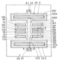
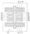
図1に、本発明の一実施形態にかかる半導体加速度センサの斜視図を示す。また、図2に図1に示す半導体加速度センサの平面図を示し、図3、図4に、図2におけるA−A断面図、B−B断面図を示す。
【0011】
図1〜図3において、基板1の上面には、単結晶シリコン(単結晶半導体材料)を溝によって分離して形成された梁構造体(可動部)2Aと固定部2Bとが配置されている。
図2、図3に示されるように、梁構造体2Aは、基板1側から突出する2つのアンカー部3a、3bにより架設されており、基板1の上面において固定部2Bから所定間隔を隔てた位置に配置されている。アンカー部3a、3bはポリシリコン薄膜よりなる。
【0012】
アンカー部3a、3bは、それぞれ梁部4、梁部5を支持している。梁部4、5は、略長方形状(多角形状)に折り曲げられた折り曲げ型の梁で構成されている。換言すれば、梁部4、5は、その長手方向が図2の左右方向となる略長方形で構成されており、内周を開口させることによって2本の梁を構成し、2つの梁の変位によって梁構造体2Aを可動とするようになっている。
【0013】
また、梁部4、5の内周の開口部分には、図2に示す梁部4、5の紙面上下方向への移動を規制するストッパー部100、101が形成されている。具体的には、図3に示すように、このストッパー部100、101は、梁構造体2Aとは分離して構成されていると共にアンカー部100a、101aにて基板49側に固定され、固定部2Bの一部を成している。そして、このストッパー部100、101は、アンカー部3a、3bを介して梁構造体2Aと電気的に接続されており、梁構造体2Aと等電位になっている。また、ストッパー部100、101は、梁部との接触面積を小さくするために部分的に突出した形状(突出部分100b、101b)で構成されており、この突出部分100b、101bが実質的なストッパーとしての役割を果たすようになっている。そして、この突出部分100b、101bは梁部4、5の端から所定の間隔(例えば2μm)をもって形成されており、この間隔以上に梁構造体2Aが移動できないようにしている。
【0014】
梁部4と梁部5との間には、長方形状を成す錘部(質量部)6が架設されている。なお、図示しないが、エッチング液の進入を行い易くするために、この錘部6の上下に貫通する透孔を形成してもよい。さらに、錘部6における一方の側面(図2においては左側面)から2つの可動電極7a、7bが突出している。この可動電極7a、7bは棒状を成し、等間隔をおいて平行に、例えば200〜400μmの長さを有して延びている。また、錘部6における他方の側面(図1においては右側面)からは2つの可動電極8a、8bが突出している。この可動電極8a、8bは棒状を成し、等間隔に平行に、例えば200〜400μmの長さを有して延びている。ここで、梁部4、5、質量部6、可動電極7a、7b、8a、8bは後述する犠牲層酸化膜の一部若しくは全部をエッチング除去することにより、可動となっている。そして、これらが可動部を構成している。
【0015】
また、基板1の上面には、2つの第1の固定電極9a、9b及び第2の固定電極11a、11bが固定されている。第1の固定電極9a、9bは基板1側から突出するアンカー部10a、10bにより支持されており、梁構造体2の各可動電極7a、7bの一方向の側面に対向して配置されている。また、第2の固定電極11a、11bは基板1側から突出するアンカー部12a、12bにより支持されており、梁構造体2の各可動電極7a、7bの他方の側面に対向して配置されている。これら第1、第2の固定電極9a、9b、11a、11bは、可動電極7a、7bと略等間隔で配置されており、梁部4、5とストッパー部100、101との間隔よりも大きい間隔(例えば2.5〜3.0μm)となっている。
【0016】
同様に、基板1の上面には、第1の固定電極13a、13b及び第2の固定電極15a、15bが固定されている。第1の固定電極13a、13bはアンカー部14a、14bにより支持され、かつ、梁構造体2の各可動電極8a、8bの一方の側面に対向して配置されている。また、第2の固定電極15a、15bは、アンカー部16a、16bにより支持され、かつ、梁構造体2の各可動電極8a、8bの他方の側面に対向して配置されている。なお、本実施形態では、可動電極及び第1、第2の固定電極を左右両側面に2つづつ設けたものを示しているが、実際には30〜100個の可動電極等を設けるようにしている。これは、可動電極等の数を増加させることにより容量を増加させ、より好適に容量検出が行えるようにするためである。
【0017】
なお、図示しないが、基板の上面には、電極取出部が形成されており、この電極取出部から可動電極及び第1、第2の固定電極による容量変化に基づく電位が取り出せるようになっている。この電極取出部は基板1から突出するアンカー部により支持されている。
基板1は、図3、図4に示すように、シリコン基板49の上に、貼り合わせ用薄膜(ポリシリコン薄膜)48とシリコン酸化膜47とシリコン窒化膜46と導電性薄膜(リン等の不純物をドーピングしたポリシリコン薄膜)45とシリコン窒化膜43とを積層した構成となっており、導電性薄膜45がシリコン窒化膜43、46の内部に埋め込まれた構造となっている。
【0018】
導電性薄膜45は、図3に示すように、アンカー部3a、3b、100a、101aを構成し、また図4に示すように、アンカー部10a、10b、12aを構成している。なお、図3、図4に図示されていないアンカー部12b、14a、14b、16a、16bについても導電性薄膜45により構成されている。
また、導電性薄膜45は、第1の固定電極9a、9bと電極取出部との間、第1の固定電極13a、13bと電極取出部との間、第2の固定電極11a、11dと電極取出部との間、及び第2の固定電極15a、15bと電極取出部との間をそれぞれ電気的に接続する配線を形成すると共に、下部電極(静電気力相殺用固定電極)26を形成している。図5に下部電極26のパターンを斜線で示す。この図に示されるように、下部電極26は基板1の上面部における梁構造体2Aと対向する領域に形成されている。
【0019】
また、図3、図4に示すように、アンカー部3aの上方にはアルミ薄膜よりなる電極(ボンディングパッド)51が設けられている。
そして、本実施形態では、さらに梁構造体2Aを構成する梁部4、5、錘部6、可動電極7a、7b、8a、8bの下部において、シリコン窒化膜43を部分的に突出させたストッパー50が形成されている。図6に、ストッパー50の形成位置を三角形で示す。この図に示されるように、梁部4、5、錘部6、可動電極7a、7b、8a、8bの下部の全ての部分に形成されている。
【0020】
上記構成において、梁構造体2Aの可動電極7a、7bと第1の固定電極9a、9bとの間に第1のコンデンサが、また梁構造体2Aの可動電極7a、7bと第2の固定電極11a、11bとの間に第2のコンデンサが形成される。同様に、梁構造体2Aの可動電極8a、8bと第1の固定電極13a、13bとの間に第1のコンデンサが、また梁構造体2Aの可動電極8a、8bと第2の固定電極15a、15bとの間に第2のコンデンサが形成される。
【0021】
そして、第1、第2のコンデンサの容量に基づいて梁構造体2Aに作用する加速度を検出できるようになっている。より詳しくは、可動電極と固定電極とにより2つの差動静電容量を形成し、2つの容量が等しくなるようにサーボ動作を行う。このような構成、作動となる本実施形態に示す加速度センサにおいて、上述したように、ストッパー50が梁部4、5、錘部6、可動電極7a、7b、8a、8bの下部全てに形成されているため、梁構造体2Aが自重によって下方に移動した時にも面積が小さなストッパー50にしか触れなくなり、犠牲層エッチング後の乾燥工程の際等において、梁構造体2Aのいずれの部分も下方の基板49側に付着しないようにすることができる。
【0022】
さらに、梁構造体2Aと下部電極26とを等電位にすることにより梁構造体2Aと基板1との間に生じる静電気力を相殺する。つまり、下部電極26はアンカー部3a、3bを通じて梁部4、5及び錘部6と結合されているため、電気的に等電位であり、梁部4、5及び静電気力により基板1に付着することを防止することができる。すなわち、梁構造体2Aはシリコン基板49に対して絶縁されているため、梁構造体2Aとシリコン基板49間のわずかな電位差によっても梁構造体2Aが基板49側に付着しようとするが、それを防止することができる。
【0023】
また、折り曲げ型の梁部4、5の内部に、部分的に突出した突出部分100b、101bを備えたストッパー部100、101を設けると共に、突出部分100b、101bと梁部4、5との間隔よりも可動電極と第1、第2の固定電極との間隔の方を大きくしているため、図2の紙面上下方向に梁構造体2Aが移動しても、可動電極と第1、第2の固定電極とが接触しないようにすることができる。このため、可動電極と第1、第2の固定電極との付着を防止することができる。そして、ストッパー部100、101を梁構造体2Aとは分離しているため、梁部4、5が共振してもストッパー部100、101が変位せず、可動電極と第1、第2の固定電極との間隔以上に梁構造体が移動することがない。このため、共振時においても固定電極と可動電極とが付着しないようにできる。
【0024】
また、ストッパー部100、101をアンカー部100a、101aを介して梁構造体2Aと等電位としているため、梁構造体2Aとストッパー部100、101との間に静電気力が発生しないようにできる。このため、静電気力による梁構造体2Aとストッパー部100、101との付着も防止できる。このように、ストッパー部100、101を梁構造体2Aとは分離して構成すると共に、突出部分100b、101bと梁部4、5との間隔を可動電極と第1、第2の固定電極との間隔よりも狭くし、さらにアンカー部100a、101aを介してストッパー部100、101と梁構造体2Aとを等電位にすることで、梁構造体2Aと固定部2Bとが付着することを防止することができる。なお、ストッパー部100、101を梁部4、5と分離して(別体で)設けているため、梁部4、5を形成するときの自由度を備えているという効果もある。
【0025】
次に、図1〜図6に示した加速度センサの製造工程を図7〜図13を用いて説明する。なお、図7〜図13は、図2におけるB−B断面での製造工程を示す概略断面図である。
〔図7に示す工程〕
まず、第1の半導体基板としての単結晶シリコン基板40を用意する。そして、このシリコン基板40にn型不純物をイオンを注入し、シリコン基板40の表層部にコンタクト用のn+ 型層40aを形成する。その後、n+ 型層40a上に犠牲層用薄膜としてのシリコン酸化膜41を熱酸化、CVD法等により成膜する。
【0026】
〔図8に示す工程〕
フォトリソグラフィにより、レジスト膜80をマスクとしてシリコン酸化膜41を一部エッチングし、凹部42を形成する。これは、犠牲層エッチング工程において梁構造体2Aがリリースされた後に表面張力等で基板に付着するのを防止すべく、付着面積を減らすために形成する。
【0027】
〔図9に示す工程〕
さらに、犠牲層エッチング時のエッチングストッパとなるシリコン窒化膜43をデポジションする。その後、シリコン酸化膜41とシリコン窒化膜との積層体に対してフォトリソグラフィを経てドライエッチング等によりアンカー部形成領域に開口部44a、44b、44c、44dを形成する。この開口部44a〜44dは、梁構造体2Aと基板(下部電極)とを接続するため、及び固定電極(及び電極取出部)と配線パターンとを接続するためのものである。
【0028】
そして、開口部44a〜44dを含むシリコン窒化膜43上に導電性薄膜となるポリシリコン薄膜45をデポジションし、その後、ポリシリコン薄膜45にリン拡散等により不純物を導入し、フォトリソグラフィを経てシリコン窒化膜43上の所定領域に配線パターン45aと下部電極45b及びアンカー部45cを形成する。そして、ポリシリコン薄膜45を含むシリコン窒化膜43上にシリコン窒化膜46をデポジションし、さらにシリコン酸化膜47をCVD法等により成膜する。
【0029】
〔図10に示す工程〕
さらに、シリコン酸化膜47の上に貼り合わせ用薄膜としてのポリシリコン薄膜48を成膜する。その後、このポリシリコン薄膜48に対して表面研磨を施し、貼り合わせ用の面として平坦化する。
〔図11に示す工程〕
シリコン基板40とは別の単結晶シリコン基板(支持板)49を用意し、ポリシリコン薄膜48の表面に貼り合わせる。
【0030】
〔図12に示す工程〕
シリコン基板40とシリコン基板49の表裏を逆にして、シリコン基板40側を表面研磨し、シリコン基板40を所望の厚さ(例えば2〜20μm)まで薄膜化する。その後、シリコン基板40にn型不純物をイオン注入し、シリコン基板40の表層部にコンタクト用のn+ 型層40bを形成する。
【0031】
〔図13に示す工程〕
シリコン基板40の所定領域に電極(パッド)51を形成したのち、フォトリソグラフィを経てシリコン基板40をエッチングし、梁部4、錘部6、可動電極7a及び第1、第2の固定電極9a、9b、11aを分離する一定幅のトレンチを形成する。なお、ここでシリコン基板40に対し、リン拡散等により不純物を導入し、後に静電容量を検出するための電極となるようにする。
【0032】
続いて、HF系のエッチング液を用いて犠牲層エッチングを行い、犠牲酸化膜を除去する。これにより、梁構造体2Aを構成する梁部4(5)、錘部6、可動電極7a(7b、8a、8b)等がリリースされ、可動となる。この際、エッチング後の乾燥の過程で可動部が基板に付着するのを防止するために、パラジクロロベンゼン等の昇華材を用いる。
【0033】
そして、凹部43が形成されていた部分は、シリコン窒化膜43が部分的に突出したストッパー50となる。
このようにして、埋め込みSOI基板を用い、配線パターン及び下部電極を絶縁体分離により形成した加速度センサを形成することができる。なお、図14は上記のように製造した図13に示す加速度センサの斜視断面図である。
【0034】
上述した実施形態においては、犠牲層用薄膜41としてシリコン酸化膜を用い、導電性薄膜45としてポリシリコン薄膜を用いているため、犠牲層エッチング工程において、HF系エッチング液を用いた場合、シリコン酸化膜はHFに溶けるがポリシリコン薄膜は溶けないので、HF系エッチング液の濃度や温度を正確に管理したり、エッチングの終了を正確なる時間管理にて行う必要がなく、製造が容易となる。
【0035】
そして、この犠牲層エッチング工程において、図8に示す凹部42により図4に示すストッパー50が形成されているので、梁構造体2Aがリリースされた後におけるエッチング液の置換工程において梁構造体2Aと基板1との間に純水等のリンス液(置換液)の液滴が残るが、この液滴の付着面積を減らして液滴による表面張力を小さくしてリンス液の蒸発の際に可動部が基板に固着するのが防止される。
【0036】
なお、従来技術として、特開平6−347474号公報に示されるセンサのように、可動電極や固定電極に突起状のストッパーを設けることにより可動電極と固定電極との接触面積を少なくし、可動電極と固定電極とが付着しないようにするものもあるが、このように可動電極や固定電極に突起状のストッパーを直接形成すると、容量が変化して正しく容量検出が行え無くなる場合があると考えられる。また、このような場合において、可動電極と固定電極との間に電位差が発生すると、静電気力によって可動電極と固定電極とが付着する場合もあるため、好ましくないといえる。
【0037】
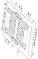
(比較例)本比較例では両持ち型の梁部を有する加速度センサの例について説明する。上記第1実施形態では、折り曲げ型の梁部を有する加速度センサを示したが、ストッパーを梁構造体2Aと分離して構成するというものは、このような折り曲げ型の梁部ではないもの、本比較例のような両持ち型の梁部を有する加速度センサにおいても適用できる。この両持ち型の梁部を有する加速度センサの斜視図を図15に示し、この図に基づいて本比較例における加速度センサを説明する。但し、第1実施形態と同様の部分については同じ符号を付し、異なる部分のみ説明する。
【0038】
梁構造体2Aは基板1から突出する4つのアンカー部150a、150b、150c、150dによって架設されており、基板1の上面において所定間隔隔てた位置に配置されている。アンカー部150a〜150dはポリシリコン薄膜よりなる。アンカー部150aとアンカー部150bとの間には梁部151が架設されており、アンカー部150cとアンカー部150dとの間には梁部152が架設されている。梁部151、152は1つの梁で構成されている。
【0039】
梁部151に対して、錘部6の反対側には、ストッパー部153が配置されている。また、梁部152に対して、錘部6の反対側には、ストッパー部154が配置されている。このストッパー部153、154に設けられた突出部153b、154bによって、梁構造体2Aの紙面左右方向への移動が規制されている。これらのストッパー部153、154は、梁構造体2Aや固定部2Bとは分離して構成されており、アンカー部153a、154aを介して基板1側に固定され、アンカー部150a〜150dを介して梁構造体2Aと電気的に接続されている。これにより、ストッパー部153、154が梁構造体2Aと等電位になるようになっている。これにより、ストッパー部153、154と梁構造体2Aとの電位差による静電気力が発生しないようにでき、静電気力によって梁構造体2Aがストッパー部153、154に付着するのを防止することができる。
【0040】
また、ストッパー部153、154は、梁部151、152との接触面積を小さくするために部分的に突出した形状(突出部分153b、154b)で構成されており、この突出部分153b、154bが実質的なストッパーとしての役割を果たすようになっている。そして、この突出部分153b、154bは梁部151、152の端から所定の間隔(例えば2μm)をもって形成されており、この間隔以上に梁構造体2Aが移動できないようにしている。なお、可動電極7a等と第1、第2の固定電極9a等との間は、梁部151、152と突出部153b、154bとの間の間隔よりも大きくなっており、梁構造体2Aが移動しても可動電極7a等が第1、第2の固定電極9a等に付着しないようになっている。
【0041】
このように、両持ち型の梁部151、152を有する加速度センサにおいても、ストッパー部153、154を梁部151、152と分離して設けると共に、ストッパー部153、154を梁部151、152と等電位とし、さらに突出部分153b、154bと梁部151、152との間よりも可動電極7a等と第1、第2の固定電極9a等との間の間隔を大きくすることにより、第1実施形態と同様の効果を得ることができる。
【0042】
なお、ストッパー部153、154を他の固定部2Bと分離せずに設け、固定部2Bの任意の箇所に設けたパッドを介して梁構造体2Aと等電位とすることも可能であるが、梁構造体2A若しくは固定部2Bに印加される電位のいずれか一方が変化した場合には、ストッパー部153、154と梁構造体2Aとの間に電位差が生じてしまうため、梁構造体2Aと直接電気的に接続することにより、このような不都合を回避することができる。また、このように他の固定部2Bと一体とした場合には、拡散層等を介してストッパー部153、154を梁構造体2Aと等電位にすることになるが、拡散抵抗等によって電位差が発生するため、ストッパー部153、154とパッドとの距離に相応して正確に等電位にすることができない。従って、本比較例のように固定部2Bと分離してストッパー部153、154を設けることにより、正確に等電位とすることができるという効果もある。
【0043】
なお、上記第1実施形態、比較例では、梁部4、5、151、152に対して錘部6の反対側に、2つづつ突出部100b、101b、153b、154bを設けるようにしているが、それよりも多くの突出部を梁部4、5、151、152の長手方向に併設するようにしてもよい。
【0044】
また、上記第1実施形態、比較例では、ストッパー部100、101と梁構造体2Aとの電気的接続をポリシリコン膜によって行っているが、シリコン基板に形成した熱拡散層等によって行うようにしてもよい。
【図面の簡単な説明】
【図1】本発明の一実施形態にかかる加速度センサの斜視図である。
【図2】図1における加速度センサの上面図である。
【図3】図2におけるA−A断面図である。
【図4】図2におけるB−B断面図である。
【図5】下部電極26を説明するための図である。
【図6】ストッパー50の形成位置を説明するための図である。
【図7】図1に示す加速度センサの製造工程を説明するための図である。
【図8】図7に続く加速度センサの製造工程を説明するための図である。
【図9】図8に続く加速度センサの製造工程を説明するための図である。
【図10】図9に続く加速度センサの製造工程を説明するための図である。
【図11】図10に続く加速度センサの製造工程を説明するための図である。
【図12】図11に続く加速度センサの製造工程を説明するための図である。
【図13】図12に続く加速度センサの製造工程を説明するための図である。
【図14】図13に示す加速度センサの斜視断面図である。
【図15】比較例に示す加速度センサの斜視図である。
【図16】従来のセンサの構造を説明するための図である。
【図17】図16に示すセンサの共振時を説明するための図である。
【符号の説明】
1…基板、2A…梁構造体、2B…固定部、3a、3b…アンカー部、
4、5…梁部、6…錘部、7a、7b、8a、8b…可動電極、
9a、9b…第1の固定電極、11a、11b…第2の固定電極、
13a、13b…第1の固定電極、15a、15b…第2の固定電極、
100、101…ストッパー部。[0001]
BACKGROUND OF THE INVENTION
The present invention relates to a semiconductor mechanical quantity sensor that has a movable part having a beam structure and detects mechanical quantities such as acceleration, yaw rate, and vibration.
[0002]
[Prior art]
In a differential capacitance type semiconductor dynamic quantity sensor that detects acceleration or the like by changing the capacitance between the movable electrode and the fixed electrode, in the drying process after the movable electrode and the fixed electrode are formed by etching, between the movable electrode and the fixed electrode. Due to the surface tension of the intervening pure water, there is a problem that the movable electrode and the fixed electrode facing it adhere to each other, and the beam and the substrate facing this adhere in the same manner. Also, at times other than the above drying process, for example, when acceleration greater than the force determined by the spring constant of the beam occurs, the van der Waals is also pulled after the movable electrode is attracted to the fixed electrode and the acceleration is reduced. There is a problem that the movable electrode and the fixed electrode adhere to each other due to the force.
[0003]
As a solution to such a problem, there is a sensor shown in US Pat. No. 5,542,295. In this sensor, a bent beam type as shown in FIG. 16 is provided with a
[0004]
[Problems to be solved by the invention]
However, in the sensor shown in the above-mentioned US Pat. No. 5,542,295, a bent beam type sensor is used, so that the stopper portion is indicated by the dotted line portion in FIG. 17 as the
[0005]
The present invention has been made in view of the above problems, and an object thereof is to provide a semiconductor dynamic quantity detection sensor in which a movable electrode and a fixed electrode are not attached even when a beam is displaced in various directions as in a resonance state. .
[0006]
[Means for Solving the Problems]
In order to achieve the above object, the present invention employs the following technical means. Claim 1 In the invention described in A movable portion (2A) and a fixed portion (2B) are provided on the substrate (1), and the movable portion includes a first anchor portion (3a, 3b) formed on the substrate and a movable electrode ( 7a, 7b, 8a, 8b) and a beam portion (4, 4) arranged to be bent so as to form a substantially polygon between the first anchor portion and the mass portion. 5), and the mass portion is supported by the first anchor portion via the beam portion, and the fixed portion has a shape facing the movable electrode, and the substrate The movable part supported by the fixed electrodes (9a, 9b, 11a, 11b, 13a, 13b, 15a, 15b) fixed on the second anchor part (100a, 101a) formed on the substrate. Stopper parts (100, 101) that restrict horizontal displacement And has the stopper portion, together with the beam portion is disposed inside the substantially polygonal configuration, it said first, and is electrically connected to the movable part through the second anchor portion It is characterized by that.
[0007]
In this way, if the fixed part separated from the movable part is provided with a stopper part, and the movement of the movable part in the horizontal direction is regulated by this stopper part, the stopper part will not be displaced even during resonance, etc. Even at times, the movable electrode and the fixed electrode can be prevented from adhering.
Furthermore, if the movable part and the stopper part are electrically connected via the first anchor part and the second anchor part, the potential difference between the movable part and the stopper part can be eliminated, so that the electrostatic force Therefore, it is possible to prevent the movable part from adhering to the stopper part.
[0010]
DETAILED DESCRIPTION OF THE INVENTION
(First embodiment)
FIG. 1 is a perspective view of a semiconductor acceleration sensor according to an embodiment of the present invention. FIG. 2 is a plan view of the semiconductor acceleration sensor shown in FIG. 1, and FIGS. 3 and 4 are sectional views taken along lines AA and BB in FIG.
[0011]
1 to 3, a beam structure (movable part) 2 </ b> A and a fixed part 2 </ b> B formed by separating single crystal silicon (single crystal semiconductor material) by grooves are arranged on the upper surface of the substrate 1. .
As shown in FIGS. 2 and 3, the beam structure 2 </ b> A is constructed by two
[0012]
The
[0013]
Further, stopper
[0014]
Between the
[0015]
In addition, two first
[0016]
Similarly, on the upper surface of the substrate 1, the first
[0017]
Although not shown, an electrode extraction portion is formed on the upper surface of the substrate, and a potential based on capacitance change by the movable electrode and the first and second fixed electrodes can be extracted from the electrode extraction portion. . The electrode extraction part is supported by an anchor part protruding from the substrate 1.
As shown in FIGS. 3 and 4, the substrate 1 is formed on a
[0018]
As shown in FIG. 3, the conductive
Further, the conductive
[0019]
Further, as shown in FIGS. 3 and 4, an electrode (bonding pad) 51 made of an aluminum thin film is provided above the
In this embodiment, a stopper in which the
[0020]
In the above configuration, the first capacitor is provided between the
[0021]
The acceleration acting on the
[0022]
Furthermore, the electrostatic force generated between the
[0023]
In addition,
[0024]
Further, the
[0025]
Next, the manufacturing process of the acceleration sensor shown in FIGS. 1 to 6 will be described with reference to FIGS. 7 to 13 are schematic cross-sectional views showing manufacturing steps at the BB cross section in FIG.
[Steps shown in FIG. 7]
First, a single
[0026]
[Steps shown in FIG. 8]
The
[0027]
[Steps shown in FIG. 9]
Further, a
[0028]
Then, a polysilicon
[0029]
[Steps shown in FIG. 10]
Further, a polysilicon
[Steps shown in FIG. 11]
A single crystal silicon substrate (support plate) 49 different from the
[0030]
[Steps shown in FIG. 12]
The
[0031]
[Steps shown in FIG. 13]
After an electrode (pad) 51 is formed in a predetermined region of the
[0032]
Subsequently, sacrificial layer etching is performed using an HF-based etchant to remove the sacrificial oxide film. Thereby, the beam part 4 (5), the
[0033]
The portion where the
In this way, it is possible to form an acceleration sensor in which a wiring pattern and a lower electrode are formed by insulator separation using a buried SOI substrate. FIG. 14 is a perspective sectional view of the acceleration sensor shown in FIG. 13 manufactured as described above.
[0034]
In the embodiment described above, a silicon oxide film is used as the sacrificial layer
[0035]
In this sacrificial layer etching step, since the
[0036]
As a conventional technique, like the sensor disclosed in JP-A-6-347474, the contact area between the movable electrode and the fixed electrode is reduced by providing a protruding stopper on the movable electrode or the fixed electrode. However, if a projecting stopper is formed directly on the movable electrode or fixed electrode in this way, the capacitance may change and the capacitance may not be detected correctly. . In such a case, if a potential difference is generated between the movable electrode and the fixed electrode, it may be undesirable because the movable electrode and the fixed electrode may adhere due to electrostatic force.
[0037]
( Comparative example )Book Comparative example Now, an example of an acceleration sensor having a double-supported beam will be described. In the first embodiment, the acceleration sensor having the folding beam portion is shown. However, the structure in which the stopper is separated from the
[0038]
The beam structure 2 </ b> A is constructed by four
[0039]
A
[0040]
The
[0041]
Thus, also in the acceleration sensor having the both-end supported
[0042]
The
[0043]
The above First 1 Embodiment Comparative example Then, two
[0044]
In addition, the above 1 Embodiment Comparative example In this case, the
[Brief description of the drawings]
FIG. 1 is a perspective view of an acceleration sensor according to an embodiment of the present invention.
2 is a top view of the acceleration sensor in FIG. 1. FIG.
FIG. 3 is a cross-sectional view taken along the line AA in FIG.
4 is a cross-sectional view taken along line BB in FIG.
FIG. 5 is a diagram for explaining a
FIG. 6 is a diagram for explaining a position where a
7 is a drawing for explaining a manufacturing process of the acceleration sensor shown in FIG. 1; FIG.
8 is a view for explaining the manufacturing process of the acceleration sensor subsequent to FIG. 7; FIG.
FIG. 9 is a view for explaining the manufacturing process of the acceleration sensor subsequent to FIG. 8;
10 is a drawing for explaining the acceleration sensor manufacturing process following FIG. 9; FIG.
11 is a view for explaining the manufacturing process for the acceleration sensor subsequent to FIG. 10; FIG.
12 is a diagram for explaining a manufacturing process of the acceleration sensor subsequent to FIG. 11. FIG.
13 is a drawing for explaining the acceleration sensor manufacturing process following FIG. 12; FIG.
14 is a perspective sectional view of the acceleration sensor shown in FIG.
FIG. 15 Comparative example It is a perspective view of the acceleration sensor shown in FIG.
FIG. 16 is a diagram for explaining the structure of a conventional sensor.
17 is a diagram for explaining a resonance time of the sensor shown in FIG. 16; FIG.
[Explanation of symbols]
DESCRIPTION OF SYMBOLS 1 ... Board | substrate, 2A ... Beam structure, 2B ... Fixed part, 3a, 3b ... Anchor part,
4, 5 ... beam part, 6 ... weight part, 7a, 7b, 8a, 8b ... movable electrode,
9a, 9b ... 1st fixed electrode, 11a, 11b ... 2nd fixed electrode,
13a, 13b ... first fixed electrode, 15a, 15b ... second fixed electrode,
100, 101: Stopper portion.
Claims (1)
前記可動部は、前記基板上に形成された第1のアンカー部(3a、3b)と、可動電極(7a、7b、8a、8b)を有する質量部(6)と、前記第1のアンカー部と前記質量部との間において略多角形を構成するように折り曲げられて配置された梁部(4、5)とを有し、前記梁部を介して前記質量部が前記第1のアンカー部に支持されるようになっており、
前記固定部は、前記可動電極と対向する形状を成し前記基板上に固定された固定電極(9a、9b、11a、11b、13a、13b、15a、15b)と、前記基板上に形成された第2のアンカー部(100a、101a)に支持され前記可動部の水平方向の変位を規制するストッパー部(100、101)とを有しており、
前記ストッパー部は、前記梁部が構成する略多角形の内側に配されていると共に、前記第1、第2のアンカー部を介して前記可動部と電気的に接続されていることを特徴とする半導体力学量センサ。The movable part (2A) and the fixed part (2B) are provided on the substrate (1),
The movable part includes a first anchor part (3a, 3b) formed on the substrate, a mass part (6) having movable electrodes (7a, 7b, 8a, 8b), and the first anchor part. And the beam portion (4, 5) disposed so as to form a substantially polygonal shape between the mass portion and the mass portion, and the mass portion is the first anchor portion via the beam portion. Has come to be supported by
The fixed part is formed on the substrate, and a fixed electrode (9a, 9b, 11a, 11b, 13a, 13b, 15a, 15b) fixed on the substrate having a shape facing the movable electrode. A stopper portion (100, 101) that is supported by the second anchor portion (100a, 101a) and regulates the displacement of the movable portion in the horizontal direction;
The stopper portion is disposed inside a substantially polygon formed by the beam portion, and is electrically connected to the movable portion via the first and second anchor portions. Semiconductor dynamic quantity sensor.
Priority Applications (3)
| Application Number | Priority Date | Filing Date | Title |
|---|---|---|---|
| JP3632598A JP3660119B2 (en) | 1998-02-18 | 1998-02-18 | Semiconductor dynamic quantity sensor |
| US09/209,414 US6065341A (en) | 1998-02-18 | 1998-12-11 | Semiconductor physical quantity sensor with stopper portion |
| DE19906046A DE19906046B4 (en) | 1998-02-18 | 1999-02-12 | Semiconductor sensors for a physical quantity with a stop section |
Applications Claiming Priority (1)
| Application Number | Priority Date | Filing Date | Title |
|---|---|---|---|
| JP3632598A JP3660119B2 (en) | 1998-02-18 | 1998-02-18 | Semiconductor dynamic quantity sensor |
Publications (2)
| Publication Number | Publication Date |
|---|---|
| JPH11230985A JPH11230985A (en) | 1999-08-27 |
| JP3660119B2 true JP3660119B2 (en) | 2005-06-15 |
Family
ID=12466698
Family Applications (1)
| Application Number | Title | Priority Date | Filing Date |
|---|---|---|---|
| JP3632598A Expired - Lifetime JP3660119B2 (en) | 1998-02-18 | 1998-02-18 | Semiconductor dynamic quantity sensor |
Country Status (1)
| Country | Link |
|---|---|
| JP (1) | JP3660119B2 (en) |
Cited By (1)
| Publication number | Priority date | Publication date | Assignee | Title |
|---|---|---|---|---|
| US9435823B2 (en) | 2013-01-11 | 2016-09-06 | Seiko Epson Corporation | Physical quantity sensor, electronic device, and moving object |
Families Citing this family (11)
| Publication number | Priority date | Publication date | Assignee | Title |
|---|---|---|---|---|
| JP2007263742A (en) * | 2006-03-28 | 2007-10-11 | Matsushita Electric Works Ltd | Capacitance type sensor |
| JP2009145321A (en) * | 2007-11-19 | 2009-07-02 | Hitachi Ltd | Inertial sensor |
| JP4799533B2 (en) * | 2007-11-19 | 2011-10-26 | Okiセミコンダクタ株式会社 | Semiconductor acceleration sensor |
| JP5079527B2 (en) * | 2008-01-08 | 2012-11-21 | 株式会社デンソー | Method for manufacturing acceleration sensor |
| JP4853530B2 (en) * | 2009-02-27 | 2012-01-11 | 株式会社豊田中央研究所 | Microdevice having movable part |
| JP5316479B2 (en) * | 2009-06-09 | 2013-10-16 | 株式会社デンソー | Manufacturing method of semiconductor dynamic quantity sensor and semiconductor dynamic quantity sensor |
| WO2011016348A1 (en) * | 2009-08-07 | 2011-02-10 | アルプス電気株式会社 | Mems sensor |
| JP6206651B2 (en) | 2013-07-17 | 2017-10-04 | セイコーエプソン株式会社 | Functional element, electronic device, and moving object |
| JP6451076B2 (en) | 2014-05-01 | 2019-01-16 | セイコーエプソン株式会社 | Functional elements, physical quantity sensors, electronic devices, and moving objects |
| JP2016042074A (en) | 2014-08-13 | 2016-03-31 | セイコーエプソン株式会社 | Physical quantity sensor, electronic apparatus and moving body |
| JP2020016557A (en) | 2018-07-26 | 2020-01-30 | セイコーエプソン株式会社 | Physical quantity sensor, electronic apparatus, and movable body |
Family Cites Families (11)
| Publication number | Priority date | Publication date | Assignee | Title |
|---|---|---|---|---|
| EP0543901B1 (en) * | 1990-08-17 | 1995-10-04 | Analog Devices, Inc. | Monolithic accelerometer |
| JPH07183543A (en) * | 1993-12-22 | 1995-07-21 | Hitachi Ltd | Acceleration sensor |
| JPH0843436A (en) * | 1994-08-03 | 1996-02-16 | Murata Mfg Co Ltd | Acceleration sensor |
| DE4431338C2 (en) * | 1994-09-02 | 2003-07-31 | Bosch Gmbh Robert | accelerometer |
| JPH08111534A (en) * | 1994-10-07 | 1996-04-30 | Nippondenso Co Ltd | Semiconductor dynamic quantity sensor and manufacture thereof |
| JP3489273B2 (en) * | 1995-06-27 | 2004-01-19 | 株式会社デンソー | Manufacturing method of semiconductor dynamic quantity sensor |
| JPH09127151A (en) * | 1995-11-01 | 1997-05-16 | Murata Mfg Co Ltd | Acceleration sensor |
| JP3430771B2 (en) * | 1996-02-05 | 2003-07-28 | 株式会社デンソー | Method of manufacturing semiconductor dynamic quantity sensor |
| JP3893636B2 (en) * | 1996-03-27 | 2007-03-14 | 日産自動車株式会社 | Manufacturing method of micromachine |
| JPH102911A (en) * | 1996-06-14 | 1998-01-06 | Hitachi Ltd | Capacitive sensor and system using it |
| JP3449130B2 (en) * | 1996-09-27 | 2003-09-22 | 日産自動車株式会社 | Dynamic quantity sensor and integrated circuit using the same |
-
1998
- 1998-02-18 JP JP3632598A patent/JP3660119B2/en not_active Expired - Lifetime
Cited By (1)
| Publication number | Priority date | Publication date | Assignee | Title |
|---|---|---|---|---|
| US9435823B2 (en) | 2013-01-11 | 2016-09-06 | Seiko Epson Corporation | Physical quantity sensor, electronic device, and moving object |
Also Published As
| Publication number | Publication date |
|---|---|
| JPH11230985A (en) | 1999-08-27 |
Similar Documents
| Publication | Publication Date | Title |
|---|---|---|
| US6065341A (en) | Semiconductor physical quantity sensor with stopper portion | |
| US6388300B1 (en) | Semiconductor physical quantity sensor and method of manufacturing the same | |
| US6276207B1 (en) | Semiconductor physical quantity sensor having movable portion and fixed portion confronted each other and method of manufacturing the same | |
| US8671757B2 (en) | Micromechanical component | |
| JP3305516B2 (en) | Capacitive acceleration sensor and method of manufacturing the same | |
| US6792804B2 (en) | Sensor for measuring out-of-plane acceleration | |
| JP4003326B2 (en) | Semiconductor dynamic quantity sensor and manufacturing method thereof | |
| JP3884795B2 (en) | Method for manufacturing structure with effective layer held away from substrate by abutment and method for separating such layer | |
| JP3307328B2 (en) | Semiconductor dynamic quantity sensor | |
| JP3660119B2 (en) | Semiconductor dynamic quantity sensor | |
| JP5091156B2 (en) | Micromechanical element and method for manufacturing micromechanical element | |
| JP4214584B2 (en) | Semiconductor dynamic quantity sensor and manufacturing method thereof | |
| JP4665942B2 (en) | Semiconductor dynamic quantity sensor | |
| US9128114B2 (en) | Capacitive sensor device and a method of sensing accelerations | |
| JPH11230986A (en) | Semiconductor dynamic quantity sensor | |
| JPH06123632A (en) | Dynamic quantity sensor | |
| JP4645656B2 (en) | Semiconductor dynamic quantity sensor | |
| KR20000028948A (en) | Method for manufacturing an angular rate sensor | |
| JP4214565B2 (en) | Manufacturing method of semiconductor dynamic quantity sensor | |
| JP4214572B2 (en) | Manufacturing method of semiconductor dynamic quantity sensor | |
| JP4557034B2 (en) | Semiconductor dynamic quantity sensor and manufacturing method thereof | |
| JP4558655B2 (en) | Semiconductor dynamic quantity sensor | |
| JP4134384B2 (en) | Manufacturing method of semiconductor dynamic quantity sensor | |
| JP3424550B2 (en) | Method of manufacturing semiconductor dynamic quantity sensor | |
| JPH11201984A (en) | Semiconductor dynamic quantity sensor and manufacture therefor |
Legal Events
| Date | Code | Title | Description |
|---|---|---|---|
| A521 | Written amendment |
Free format text: JAPANESE INTERMEDIATE CODE: A523 Effective date: 20050218 |
|
| A61 | First payment of annual fees (during grant procedure) |
Free format text: JAPANESE INTERMEDIATE CODE: A61 Effective date: 20050316 |
|
| R150 | Certificate of patent or registration of utility model |
Free format text: JAPANESE INTERMEDIATE CODE: R150 |
|
| FPAY | Renewal fee payment (event date is renewal date of database) |
Free format text: PAYMENT UNTIL: 20110325 Year of fee payment: 6 |
|
| FPAY | Renewal fee payment (event date is renewal date of database) |
Free format text: PAYMENT UNTIL: 20120325 Year of fee payment: 7 |
|
| FPAY | Renewal fee payment (event date is renewal date of database) |
Free format text: PAYMENT UNTIL: 20120325 Year of fee payment: 7 |
|
| FPAY | Renewal fee payment (event date is renewal date of database) |
Free format text: PAYMENT UNTIL: 20130325 Year of fee payment: 8 |
|
| FPAY | Renewal fee payment (event date is renewal date of database) |
Free format text: PAYMENT UNTIL: 20140325 Year of fee payment: 9 |
|
| R250 | Receipt of annual fees |
Free format text: JAPANESE INTERMEDIATE CODE: R250 |
|
| R250 | Receipt of annual fees |
Free format text: JAPANESE INTERMEDIATE CODE: R250 |
|
| R250 | Receipt of annual fees |
Free format text: JAPANESE INTERMEDIATE CODE: R250 |
|
| R250 | Receipt of annual fees |
Free format text: JAPANESE INTERMEDIATE CODE: R250 |
|
| EXPY | Cancellation because of completion of term |