JP3649880B2 - Liquid crystal display device manufacturing method - Google Patents
Liquid crystal display device manufacturing method Download PDFInfo
- Publication number
- JP3649880B2 JP3649880B2 JP31335597A JP31335597A JP3649880B2 JP 3649880 B2 JP3649880 B2 JP 3649880B2 JP 31335597 A JP31335597 A JP 31335597A JP 31335597 A JP31335597 A JP 31335597A JP 3649880 B2 JP3649880 B2 JP 3649880B2
- Authority
- JP
- Japan
- Prior art keywords
- substrates
- liquid crystal
- spacer
- gap
- crystal display
- Prior art date
- Legal status (The legal status is an assumption and is not a legal conclusion. Google has not performed a legal analysis and makes no representation as to the accuracy of the status listed.)
- Expired - Fee Related
Links
Images
Landscapes
- Liquid Crystal (AREA)
Description
【0001】
【発明の属する技術分野】
本発明は2枚の基板のギャップが一定に調整され得る液晶表示素子およびその製法に関する。さらに詳しくは、スペーサがその径を調整し得るように形成されることにより、基板の貼着前または貼着後にその基板ギャップが調整され得る液晶表示素子の製法に関する。
【0002】
【従来の技術】
液晶表示素子は、2枚のガラス板などからなる絶縁性透明基板にそれぞれ透明電極や配向膜などが設けられ、一方の基板のセル周囲にシール剤が設けられ、他方の基板にスペーサが散布されて2枚の基板がそれぞれ透明電極や配向膜が対向するようにスペーサを介して一定間隙を有するように貼着され、各セルに分割した後に2枚の基板の間隙に液晶材料が充填され、その両外面に偏光板などが貼着されることにより製造される。
【0003】
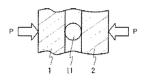
このスペーサは、たとえばガラスなどの球状または円柱状のものからなり、その径が予め所望の基板間隔(ギャップ)を得るための大きさに形成されたものを空気中に噴霧させて基板上に沈降させることにより散布される。その後、基板を搬送して他方の基板を重ね合わせて貼着される。そのため、散布自体が基板の全面で完全には均等に散布されなかったり、その後の搬送時などに動いて必ずしも均等には分布していない。このスペーサが固まって存在する部分では基板のギャップが大きくなり、基板間隔が均一にならない。スーパーツイストネマティック(STN)液晶が用いられる液晶表示素子ではとくにギャップのバラツキによる表示品位の低下が顕著となる。そのため、シール剤により貼着した後に、図3に概念図が示されるように、シール剤により貼着されたガラス基板1、2の両側から2kg/cm2 程度の圧力Pを加えて1分程度の一定時間放置するというギャップ調整工程が必要となる。なお、図3で11はスペーサである。このギャップ調整工程は、ゴムシートなどを介して数セット乃至10セット程度を重ねて行われるが、バッチ処理で行わざるを得ず、ベルトコンベヤ式に枚葉処理をすることができない。
【0004】
また、シール剤に混入される第2のスペーサもガラスの円柱状のものが使用されるが、カラーフィルタの有る無しなどによっても液晶層の厚さが変るなど液晶表示素子の種類によって微妙にその間隙が異なり、各機種ごとにその大きさの異なるスペーサを準備しなければならない。
【0005】
【発明が解決しようとする課題】
上述のように、従来の液晶表示素子では、2枚の基板間に介在させるスペーサが均等に分布されず、スペーサがたくさん固まったところでは基板のギャップが大きくなり、基板間隔が場所により異なって表示品位が低下するという問題がある。これを防止するためにギャップ調整工程を設けると、その工程がバッチ処理となり、自動的な製造ラインの流れの妨げとなると共に、調整したものが後から戻ってギャップの不均一が生じるという問題がある。
【0006】
さらに、液晶表示素子の機種によってシール剤に混入する第2のスペーサの大きさが異なり、何種類ものスペーサを準備すると、コストアップになると共に、わずかに大きさの異なるスペーサを製造工程で管理するのは非常に煩わしく、相互に混入しやすいという問題がある。
【0007】
本発明は、このような問題を解決するためになされたもので、スペーサがたくさん固まって基板のギャップが広くなった場合でも、後からそのギャップを調整し得る液晶表示素子の製法を提供することにある。
【0008】
本発明の他の目的は、僅かに大きさの異なるスペーサを予め形成しておかなくても、必要な大きさのスペーサをその都度調製することにより、所望の基板ギャップを得ることができる液晶表示素子の製法を提供することにある。
【0010】
【課題を解決するための手段】
本発明による液晶表示素子の製法は、2枚の基板にそれぞれ電極パターンおよび配向膜を形成し、該2枚の基板の一方に少なくとも中心部は完全には硬化していない紫外線硬化性樹脂からなるスペーサを散布し、前記2枚の基板を前記スペーサを介した間隙でその周囲でシール剤により貼着し、貼着された2枚の基板の間隔を測定し、間隔の大きい部分の前記スペーサに紫外線を照射して前記スペーサの完全には硬化していない紫外線硬化性樹脂を硬化させることにより、体積を小さくして前記2枚の基板の間隙を一定にし、該間隙に液晶材料を注入することを特徴とする。
具体的には、前記紫外線の照射を、ギャップ測定器により前記2枚の基板間隔を測定し、該測定値に基づいて紫外線照射量算出器により所定の間隔にするための紫外線照射量を算出し、該算出した量の紫外線を照射することにより行うことができる。
【0011】
本発明による液晶表示素子の製法の他の形態は、2枚の基板にそれぞれ電極パターンおよび配向膜を形成し、該2枚の基板をその間にスペーサを介在させてその周囲で第2のスペーサを混入したシール剤により貼着し、貼着された2枚の基板の間隙部に液晶材料を注入する液晶表示素子の製法であって、前記第2のスペーサを少なくとも中心部が完全には硬化していない紫外線硬化性樹脂により形成し、前記シール剤に混入する前に紫外線を照射することにより該第2のスペーサを所定の大きさに調整してから前記シール剤に混入することを特徴とする。ここに硬化状態により体積変化率の大きい材料とは、たとえば紫外線硬化性樹脂で紫外線の照射量により硬化状態が変化するときにその体積が大きく変化する材料を意味し、熱硬化性のエポキシ樹脂なども含まれる。
【0012】
【発明の実施の形態】
つぎに、図面を参照しながら本発明の液晶表示素子の製法について説明をする。
【0013】
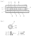
本発明の製法により得られる液晶表示素子は、図1(a)に示されるように、ガラスなどからなる絶縁性透明基板1、2の一面側にそれぞれITOなどからなる電極パターン3、4が設けられ、その表面にそれぞれポリイミドなどからなる配向膜5、6が設けられている。そして、2枚の基板1、2が一定間隙を有して対向するようにその間にスペーサ11が介在されており、その周囲がシール剤7により貼着されている。そして、その間隙に液晶材料が充填されて液晶層8が形成されている。絶縁性透明基板1、2の外表面には、偏光板9、10が貼着されている。この液晶パネルの構成は、通常の液晶パネルの構成と同じで、本発明では、スペーサ11に、図1(b)に示されるように、少なくともその中心部が紫外線硬化性樹脂からなるスペーサが用いられていることに特徴がある。
【0014】
スペーサ11は、図1(b)に示されるように、中心部を占める紫外線硬化性樹脂部11aと、その外周を取り巻く外殻11bとからなっている。紫外線硬化性樹脂部11aは、一方の基板上に散布される前の段階では、完全には硬化していない状態で所望のギャップが得られるように形成されている。その完全に硬化していない紫外線硬化性樹脂部11aを保護するため、その周囲に外殻11bが設けられている。この外殻11bは、たとえば紫外線硬化性樹脂の硬化した部分で形成されていてもよい。すなわち、たとえば液状の紫外線硬化性樹脂をエアーなどを用いて霧状にし、短時間紫外線を照射することにより、内部までは硬化せず、外表面だけを硬化させて外殻11bを形成することができる。この外殻11bは、エポキシ樹脂などなんでもよく、たとえばある程度硬化させた紫外線硬化樹脂のビーズ状のものの周囲にエポキシ樹脂などを被覆したものでもよい。
【0015】
この少なくとも中心部が紫外線硬化性樹脂からなるスペーサ11は、硬化が進むにつれてその体積の変化率が非常に大きい。たとえば液状の体積と、中程度に硬化した状態と、完全に硬化させた状態での体積比は、111:105:100と変化率が大きい。そのため、基板に散布する前のスペーサとして、完全に硬化させないで所定の大きさのスペーサを作製しておくことにより、基板を貼着した後から紫外線を照射して完全に硬化させるとその直径は3.5%程度は小さくなる。一方、中程度に硬化しておれば、液晶パネルの基板表面に印加される外力に対してはスペーサに集中的に外力が加わるわけではないため、充分に機械的強度が得られる。そのため、液晶パネルのギャップが得られて紫外線硬化性樹脂を完全に硬化させない場合でも、問題は生じない。
【0016】
つぎに、このスペーサを用いて、液晶パネルの基板のギャップを調整する方法、すなわち本発明の液晶表示素子の製法について説明をする。
【0017】
まず、電極パターンおよび配向膜などが設けられた基板の一方に少なくとも中心部が完全には硬化していない紫外線硬化性樹脂からなるスペーサを散布し、シール剤が印刷された他方の基板を重ね合わせて周囲で貼着する。この基板の貼着の際には、シール在中に柱状のガラス棒などからなる第2のスペーサが混入されており、基板の両面から一定の圧力を印加して加熱しながらシール剤の熱硬化性エポキシ樹脂を硬化させる。そのため、この貼着部分はほぼ一定の間隙で貼着されるが、シール剤から離れた部分では前述のように、スペーサの分布などによりそのギャップにバラツキが生じる。
【0018】
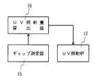
つぎに、図2に概略のブロック図が示されるように、ギャップ測定器15により基板間のギャップを測定する。この基板間のギャップの測定は、たとえばキャノン(株)製の商品名TM−005Sなどを用いることにより、平面上に載置される貼着された基板間のギャップを即座に測定することができる。この測定値が紫外線(UV)照射量の算出器16に送られ、そこで必要な照射量を計算する。そして、何秒照射するかの指示をUV照射炉17に送り、所定の時間UVを照射する。このループを所定のギャップが得られるまで繰り返し、基板の全面に同様の工程を繰り返すことにより、自動的に全面で均一なギャップを有する貼着された基板が得られる。
【0019】
その後、基板の間隙部に液晶材料を注入して封止し、正面に偏光板を貼着することにより液晶表示素子が得られる。
【0020】
本発明によれば、スペーサに少なくともその中心部が紫外線硬化性樹脂で形成されたものを使用しているため、硬化状態によりその体積変化が大きく、2枚の基板を貼着した後に、その基板のギャップを測定しながら紫外線を照射することにより、スペーサの径を調整することができる。その結果、スペーサの散布状況によりギャップのバラツキが生じても、部分的にそのギャップを調整をすることができ、全面で均一なギャップとなり、表示品位の優れた液晶表示素子が得られる。しかも、ギャップを測定しながら紫外線を照射するだけで調整をすることができるため、製造ラインの自動工程に合せて連続的に枚葉処理をすることができる。
【0021】
前述の例では、液晶材料が注入される基板間隙部のスペーサにUV樹脂製のものを使用し、シール剤中に混入する第2のスペーサには従来と同様のガラス製の円柱状のものまたは球形状のものを使用した。しかし、液晶表示素子の機種が異なると、微妙に基板のギャップを異ならせる必要があり、この第2のスペーサも何種類のものが準備されてそれぞれに使い分けられている。この第2のスペーサにも前述の紫外線硬化性樹脂のように、体積の変化の大きい材料からなるものを使用し、たとえば外殻が固く、中心部は完全には硬化していない紫外線硬化性樹脂からなる直径がたとえば6.5μm程度のものを準備しておき、使用の都度紫外線を照射してその直径がたとえば6.3μm、6.4μmなどの大きさのスペーサにすることにより、何種類のものを準備して、別々に保管しなくても済むため、非常に製造管理が容易になると共にコストダウンにもなる。この場合は、前述の基板間に組み込んでからの調整ではないため、スペーサに直接熱を加えて温度上昇をさせることができ、エポキシ樹脂などでもその大きさを変化させることができる。また、形状もビーズ状に限らず、円柱状のものを形成しておき、その直径を変化させることができる。円柱状のものを製造する場合には、たとえば所望の太さの筒体から液状のものを押し出しながら表面を硬化させることにより外殻を有する内部の硬化が完全でないものを作ることができ、それを切断することにより形成することができる。
【0022】
【発明の効果】
本発明によれば、スペーサの分布に拘らず、加圧してギャップ調整をしなくても、基板のギャップを全面で均一にすることができるため、ギャップに敏感なSTN液晶を用いる場合でも表示品位の優れた液晶表示素子が得られる。
【0023】
さらに、シール剤に混入する第2のスペーサにも紫外線樹脂などの体積変化の大きい材料を用いることにより、ギャップの種類が何種類もある場合でも、第2のスペーサの体積を変化させて大きさを調整してから混入することにより、スペーサを共通化することができ、使用の都度必要な寸法のスペーサにすることができる。そのため、スペーサの種類を何種類も準備する必要がなく、コストダウンに寄与すると共に、部品管理も容易になる。
【図面の簡単な説明】
【図1】本発明の液晶表示素子の一実施形態の断面説明図である。
【図2】本発明の液晶表示素子の製法の一実施形態の基板間のギャップを調整する手段のブロック図である。
【図3】従来の液晶表示素子のギャップを調整する方法を概念的に示す図である。
【符号の説明】
1、2 基板
3、4 電極パターン
5、6 配向膜
7 シール剤
8 液晶層
11 スペーサ[0001]
BACKGROUND OF THE INVENTION
The present invention relates to a liquid crystal display element in which a gap between two substrates can be adjusted to be constant and a method for manufacturing the same. More particularly, by being formed so as spacers can adjust its size relates to a process for the production of liquid crystal display element in which the substrate gap before or after sticking sticking of the substrate can be adjusted.
[0002]
[Prior art]
In a liquid crystal display element, an insulating transparent substrate made of two glass plates or the like is provided with a transparent electrode, an alignment film, etc., a sealing agent is provided around the cell of one substrate, and spacers are scattered on the other substrate. The two substrates are attached so as to have a constant gap through a spacer so that the transparent electrode and the alignment film face each other, and after dividing into each cell, the gap between the two substrates is filled with a liquid crystal material, Manufactured by sticking polarizing plates or the like to both outer surfaces.
[0003]
This spacer is made of, for example, glass or a spherical or cylindrical shape, and its diameter is set in advance to obtain a desired substrate interval (gap) and sprayed into the air to settle on the substrate. It is spread by letting. Thereafter, the substrate is transported and the other substrate is laminated and pasted. For this reason, the spraying itself is not completely evenly distributed over the entire surface of the substrate, or it is not necessarily evenly distributed due to movement during subsequent transport. In the portion where the spacer is solidified, the gap between the substrates becomes large, and the interval between the substrates is not uniform. In a liquid crystal display element using a super twist nematic (STN) liquid crystal, the display quality is particularly deteriorated due to gap variations. Therefore, after sticking with a sealing agent, as shown in the conceptual diagram of FIG. 3, a pressure P of about 2 kg / cm 2 is applied from both sides of the
[0004]
In addition, the second spacer mixed in the sealant is also a glass column, but the thickness of the liquid crystal layer changes depending on whether the color filter is present or not. Spacers are different, and spacers of different sizes must be prepared for each model.
[0005]
[Problems to be solved by the invention]
As described above, in the conventional liquid crystal display element, the spacers interposed between the two substrates are not evenly distributed, and when the spacers are hardened, the gap between the substrates becomes large, and the distance between the substrates varies depending on the location. There is a problem that the quality is lowered. If a gap adjustment process is provided to prevent this, the process becomes a batch process, and the flow of the automatic production line is hindered. is there.
[0006]
Furthermore, the size of the second spacer mixed in the sealant differs depending on the model of the liquid crystal display element. If several types of spacers are prepared, the cost increases, and spacers having slightly different sizes are managed in the manufacturing process. Is very troublesome and has the problem of being easily mixed with each other.
[0007]
The present invention has been made to solve this problem, the spacer is to provide a process for the preparation of liquid crystal display element capable of adjusting the gap later, even if the gap of the substrate is wider solidified lot There is.
[0008]
Another object of the present invention is to provide a liquid crystal display capable of obtaining a desired substrate gap by preparing a spacer having a required size each time without forming a spacer having a slightly different size in advance. It is to provide a method for manufacturing an element.
[0010]
[Means for Solving the Problems]
The method for producing a liquid crystal display device according to the present invention comprises forming an electrode pattern and an alignment film on two substrates, respectively, and comprising an ultraviolet curable resin at least at the center of which is not completely cured on one of the two substrates. spraying spacers, the two substrates bonded by a sealing agent around in the gap via the spacers, to measure the distance between the two substrates which are bonded to the spacer a large portion of the distance Irradiating ultraviolet rays to cure the UV curable resin that is not completely cured of the spacer, thereby reducing the volume and making the gap between the two substrates constant, and injecting a liquid crystal material into the gap It is characterized by.
Specifically, the ultraviolet irradiation is measured by measuring the distance between the two substrates with a gap measuring device, and calculating the ultraviolet irradiation dose for making the predetermined interval with the ultraviolet irradiation amount calculator based on the measured value. The irradiation can be performed by irradiating the calculated amount of ultraviolet rays .
[0011]
In another embodiment of the method for manufacturing a liquid crystal display device according to the present invention, an electrode pattern and an alignment film are formed on two substrates, respectively, a spacer is interposed between the two substrates, and a second spacer is formed around the spacer. A method of manufacturing a liquid crystal display element in which a liquid crystal material is injected into a gap between two bonded substrates by adhering with a mixed sealant, and at least a central portion of the second spacer is completely cured. The second spacer is adjusted to a predetermined size by irradiating with ultraviolet rays before being mixed with the sealant, and then mixed with the sealant. . Here, a material having a large volume change rate depending on the cured state means, for example, a material whose volume changes greatly when the cured state changes depending on the irradiation amount of ultraviolet rays in an ultraviolet curable resin, such as a thermosetting epoxy resin. Is also included.
[0012]
DETAILED DESCRIPTION OF THE INVENTION
Next, a description method for producing the liquid crystal display element of the present invention with reference to the drawings.
[0013]
As shown in FIG. 1A, the liquid crystal display element obtained by the manufacturing method of the present invention is provided with
[0014]
As shown in FIG. 1B, the
[0015]
The
[0016]
Next, a method for adjusting the gap of the substrate of the liquid crystal panel using this spacer, that is, a method for producing the liquid crystal display element of the present invention will be described.
[0017]
First, a spacer made of an ultraviolet curable resin whose central portion is not completely cured is sprayed on one of the substrates provided with an electrode pattern and an alignment film, and the other substrate on which the sealant is printed is overlaid. And stick around. During the sticking of the substrate, a second spacer made of a columnar glass rod or the like is mixed during the sealing, and the sealant is thermally cured while being heated by applying a certain pressure from both sides of the substrate. The epoxy resin is cured. Therefore, although this sticking part is stuck with a substantially constant gap, as described above, the gap varies due to the distribution of spacers, etc., in the part away from the sealant.
[0018]
Next, as shown in a schematic block diagram in FIG. 2, the
[0019]
After that, a liquid crystal material is injected into the gap portion of the substrate and sealed, and a polarizing plate is attached to the front surface to obtain a liquid crystal display element.
[0020]
According to the present invention, since a spacer having at least its central portion formed of an ultraviolet curable resin is used, the volume change is large depending on the cured state, and after the two substrates are pasted, the substrate The diameter of the spacer can be adjusted by irradiating ultraviolet rays while measuring the gap. As a result, even if the gap varies due to the dispersion state of the spacers, the gap can be partially adjusted, resulting in a uniform gap on the entire surface, and a liquid crystal display element with excellent display quality can be obtained. In addition, since adjustment can be performed simply by irradiating ultraviolet rays while measuring the gap, single wafer processing can be continuously performed in accordance with the automatic process of the production line.
[0021]
In the above-described example, a UV resin spacer is used as a spacer in the substrate gap portion into which the liquid crystal material is injected, and the second spacer mixed in the sealant is a glass columnar member similar to the conventional one or A spherical shape was used. However, if the types of liquid crystal display elements are different, it is necessary to slightly change the gap between the substrates, and several types of second spacers are prepared and used differently. The second spacer is also made of a material having a large volume change such as the aforementioned ultraviolet curable resin. For example, an ultraviolet curable resin whose outer shell is hard and whose central portion is not completely cured is used. By preparing a spacer having a diameter of, for example, about 6.5 μm, and irradiating it with ultraviolet rays each time it is used, the diameter of the spacer becomes, for example, 6.3 μm, 6.4 μm, etc. Since it is not necessary to prepare and store them separately, manufacturing management becomes very easy and the cost is reduced. In this case, since the adjustment is not performed after the substrate is incorporated between the substrates, the temperature can be increased by directly applying heat to the spacer, and the size can be changed even with an epoxy resin or the like. Further, the shape is not limited to the bead shape, and a cylindrical shape can be formed and its diameter can be changed. In the case of manufacturing a cylindrical product, for example, by curing a surface while extruding a liquid material from a cylindrical body having a desired thickness, it is possible to make a product having an inner shell that is not completely cured, Can be formed by cutting.
[0022]
【The invention's effect】
According to the present invention, the gap of the substrate can be made uniform over the entire surface without adjusting the gap by applying pressure regardless of the spacer distribution. Therefore, even when STN liquid crystal sensitive to the gap is used, the display quality is improved. Excellent liquid crystal display element.
[0023]
Further, by using a material having a large volume change such as an ultraviolet resin for the second spacer mixed in the sealant, the volume of the second spacer can be changed and the size can be changed even when there are many kinds of gaps. By mixing after adjusting, the spacer can be made common, and a spacer having a required dimension can be obtained each time it is used. Therefore, it is not necessary to prepare various types of spacers, contributing to cost reduction and facilitating component management.
[Brief description of the drawings]
FIG. 1 is a cross-sectional explanatory view of an embodiment of a liquid crystal display element of the present invention.
FIG. 2 is a block diagram of a means for adjusting a gap between substrates in an embodiment of a method for producing a liquid crystal display element of the present invention.
FIG. 3 is a diagram conceptually illustrating a method for adjusting a gap of a conventional liquid crystal display element.
[Explanation of symbols]
1, 2
Claims (3)
Priority Applications (1)
| Application Number | Priority Date | Filing Date | Title |
|---|---|---|---|
| JP31335597A JP3649880B2 (en) | 1997-11-14 | 1997-11-14 | Liquid crystal display device manufacturing method |
Applications Claiming Priority (1)
| Application Number | Priority Date | Filing Date | Title |
|---|---|---|---|
| JP31335597A JP3649880B2 (en) | 1997-11-14 | 1997-11-14 | Liquid crystal display device manufacturing method |
Publications (2)
| Publication Number | Publication Date |
|---|---|
| JPH11142859A JPH11142859A (en) | 1999-05-28 |
| JP3649880B2 true JP3649880B2 (en) | 2005-05-18 |
Family
ID=18040265
Family Applications (1)
| Application Number | Title | Priority Date | Filing Date |
|---|---|---|---|
| JP31335597A Expired - Fee Related JP3649880B2 (en) | 1997-11-14 | 1997-11-14 | Liquid crystal display device manufacturing method |
Country Status (1)
| Country | Link |
|---|---|
| JP (1) | JP3649880B2 (en) |
Families Citing this family (1)
| Publication number | Priority date | Publication date | Assignee | Title |
|---|---|---|---|---|
| JP7463093B2 (en) * | 2019-12-24 | 2024-04-08 | 株式会社ジャパンディスプレイ | Pressing force sensor |
Family Cites Families (8)
| Publication number | Priority date | Publication date | Assignee | Title |
|---|---|---|---|---|
| JP2514993B2 (en) * | 1987-12-09 | 1996-07-10 | 株式会社東芝 | Liquid crystal display manufacturing method |
| JPH0830812B2 (en) * | 1988-11-09 | 1996-03-27 | 松下電器産業株式会社 | Semiconductor device and method for forming spacer thereof |
| JPH05100232A (en) * | 1990-12-05 | 1993-04-23 | Toshiba Corp | Liquid crystal display |
| JP2939836B2 (en) * | 1991-03-29 | 1999-08-25 | カシオ計算機株式会社 | Liquid crystal display device |
| JP2953594B2 (en) * | 1991-04-18 | 1999-09-27 | 大日本印刷株式会社 | Liquid crystal display and color filter |
| JPH0527246A (en) * | 1991-07-22 | 1993-02-05 | Matsushita Electric Ind Co Ltd | LCD panel |
| JPH0894995A (en) * | 1994-09-28 | 1996-04-12 | Teijin Ltd | Manufacturing method for minute dots and touch panel |
| JPH117027A (en) * | 1997-06-16 | 1999-01-12 | Canon Inc | Adhesive spacer, liquid crystal element using the same and method of manufacturing the same |
-
1997
- 1997-11-14 JP JP31335597A patent/JP3649880B2/en not_active Expired - Fee Related
Also Published As
| Publication number | Publication date |
|---|---|
| JPH11142859A (en) | 1999-05-28 |
Similar Documents
| Publication | Publication Date | Title |
|---|---|---|
| JP2654940B2 (en) | Manufacturing method of electro-optical element | |
| JP2003186026A (en) | Liquid crystal display device and method of manufacturing the same | |
| JPH05127179A (en) | Production of liquid crystal display element | |
| JPS60200228A (en) | Spacer for liquid crystal display device | |
| WO2015106539A1 (en) | Frame sealing glue coating method and device, and display device | |
| JP3649880B2 (en) | Liquid crystal display device manufacturing method | |
| JP4209146B2 (en) | Liquid crystal display element and manufacturing method thereof | |
| JP2009198865A (en) | Bonding method for liquid crystal panel | |
| JP3315063B2 (en) | Printing plate for forming a thin film and method for forming a thin film using the printing plate for forming a thin film | |
| JP3273164B2 (en) | Liquid crystal panel manufacturing method and manufacturing apparatus | |
| JP2823420B2 (en) | Liquid crystal display device | |
| JP4021258B2 (en) | Liquid crystal display device manufacturing method | |
| JP3402056B2 (en) | Manufacturing method of liquid crystal display element | |
| JPH05297383A (en) | Production of liquid crystal display element | |
| JP4137512B2 (en) | Manufacturing method of liquid crystal display device | |
| JP2878521B2 (en) | Manufacturing method of liquid crystal display element | |
| JP2001075111A (en) | Manufacture of liquid crystal device | |
| JPH0561051A (en) | Liquid crystal display device and production thereof | |
| JPS6132035A (en) | Production of liquid crystal display element | |
| JP2000187225A (en) | Manufacturing method of liquid crystal display device | |
| JPS63220115A (en) | Liquid crystal display element | |
| JP2002098975A (en) | Liquid crystal device manufacturing method | |
| JP3666943B2 (en) | Manufacturing method of liquid crystal display device | |
| JPH05165037A (en) | Manufacture of liquid crystal panel | |
| JPH02310525A (en) | Production of liquid crystal display device |
Legal Events
| Date | Code | Title | Description |
|---|---|---|---|
| A977 | Report on retrieval |
Free format text: JAPANESE INTERMEDIATE CODE: A971007 Effective date: 20040805 |
|
| A131 | Notification of reasons for refusal |
Free format text: JAPANESE INTERMEDIATE CODE: A131 Effective date: 20040831 |
|
| A521 | Written amendment |
Free format text: JAPANESE INTERMEDIATE CODE: A523 Effective date: 20041101 |
|
| TRDD | Decision of grant or rejection written | ||
| A01 | Written decision to grant a patent or to grant a registration (utility model) |
Free format text: JAPANESE INTERMEDIATE CODE: A01 Effective date: 20050215 |
|
| A61 | First payment of annual fees (during grant procedure) |
Free format text: JAPANESE INTERMEDIATE CODE: A61 Effective date: 20050216 |
|
| R150 | Certificate of patent or registration of utility model |
Free format text: JAPANESE INTERMEDIATE CODE: R150 |
|
| LAPS | Cancellation because of no payment of annual fees |