JP3638530B2 - Reference current circuit and reference voltage circuit - Google Patents
Reference current circuit and reference voltage circuit Download PDFInfo
- Publication number
- JP3638530B2 JP3638530B2 JP2001036139A JP2001036139A JP3638530B2 JP 3638530 B2 JP3638530 B2 JP 3638530B2 JP 2001036139 A JP2001036139 A JP 2001036139A JP 2001036139 A JP2001036139 A JP 2001036139A JP 3638530 B2 JP3638530 B2 JP 3638530B2
- Authority
- JP
- Japan
- Prior art keywords
- transistor
- current
- circuit
- resistor
- voltage
- Prior art date
- Legal status (The legal status is an assumption and is not a legal conclusion. Google has not performed a legal analysis and makes no representation as to the accuracy of the status listed.)
- Expired - Fee Related
Links
Images


Classifications
-
- G—PHYSICS
- G05—CONTROLLING; REGULATING
- G05F—SYSTEMS FOR REGULATING ELECTRIC OR MAGNETIC VARIABLES
- G05F3/00—Non-retroactive systems for regulating electric variables by using an uncontrolled element, or an uncontrolled combination of elements, such element or such combination having self-regulating properties
- G05F3/02—Regulating voltage or current
- G05F3/08—Regulating voltage or current wherein the variable is dc
- G05F3/10—Regulating voltage or current wherein the variable is dc using uncontrolled devices with non-linear characteristics
- G05F3/16—Regulating voltage or current wherein the variable is dc using uncontrolled devices with non-linear characteristics being semiconductor devices
- G05F3/20—Regulating voltage or current wherein the variable is dc using uncontrolled devices with non-linear characteristics being semiconductor devices using diode- transistor combinations
- G05F3/26—Current mirrors
- G05F3/267—Current mirrors using both bipolar and field-effect technology
-
- G—PHYSICS
- G05—CONTROLLING; REGULATING
- G05F—SYSTEMS FOR REGULATING ELECTRIC OR MAGNETIC VARIABLES
- G05F3/00—Non-retroactive systems for regulating electric variables by using an uncontrolled element, or an uncontrolled combination of elements, such element or such combination having self-regulating properties
- G05F3/02—Regulating voltage or current
- G05F3/08—Regulating voltage or current wherein the variable is dc
- G05F3/10—Regulating voltage or current wherein the variable is dc using uncontrolled devices with non-linear characteristics
- G05F3/16—Regulating voltage or current wherein the variable is dc using uncontrolled devices with non-linear characteristics being semiconductor devices
- G05F3/20—Regulating voltage or current wherein the variable is dc using uncontrolled devices with non-linear characteristics being semiconductor devices using diode- transistor combinations
- G05F3/30—Regulators using the difference between the base-emitter voltages of two bipolar transistors operating at different current densities
-
- G—PHYSICS
- G05—CONTROLLING; REGULATING
- G05F—SYSTEMS FOR REGULATING ELECTRIC OR MAGNETIC VARIABLES
- G05F3/00—Non-retroactive systems for regulating electric variables by using an uncontrolled element, or an uncontrolled combination of elements, such element or such combination having self-regulating properties
- G05F3/02—Regulating voltage or current
- G05F3/08—Regulating voltage or current wherein the variable is dc
- G05F3/10—Regulating voltage or current wherein the variable is dc using uncontrolled devices with non-linear characteristics
- G05F3/16—Regulating voltage or current wherein the variable is dc using uncontrolled devices with non-linear characteristics being semiconductor devices
- G05F3/20—Regulating voltage or current wherein the variable is dc using uncontrolled devices with non-linear characteristics being semiconductor devices using diode- transistor combinations
- G05F3/26—Current mirrors
- G05F3/262—Current mirrors using field-effect transistors only
-
- G—PHYSICS
- G05—CONTROLLING; REGULATING
- G05F—SYSTEMS FOR REGULATING ELECTRIC OR MAGNETIC VARIABLES
- G05F3/00—Non-retroactive systems for regulating electric variables by using an uncontrolled element, or an uncontrolled combination of elements, such element or such combination having self-regulating properties
- G05F3/02—Regulating voltage or current
- G05F3/08—Regulating voltage or current wherein the variable is dc
- G05F3/10—Regulating voltage or current wherein the variable is dc using uncontrolled devices with non-linear characteristics
- G05F3/16—Regulating voltage or current wherein the variable is dc using uncontrolled devices with non-linear characteristics being semiconductor devices
- G05F3/20—Regulating voltage or current wherein the variable is dc using uncontrolled devices with non-linear characteristics being semiconductor devices using diode- transistor combinations
- G05F3/26—Current mirrors
- G05F3/265—Current mirrors using bipolar transistors only
-
- Y—GENERAL TAGGING OF NEW TECHNOLOGICAL DEVELOPMENTS; GENERAL TAGGING OF CROSS-SECTIONAL TECHNOLOGIES SPANNING OVER SEVERAL SECTIONS OF THE IPC; TECHNICAL SUBJECTS COVERED BY FORMER USPC CROSS-REFERENCE ART COLLECTIONS [XRACs] AND DIGESTS
- Y10—TECHNICAL SUBJECTS COVERED BY FORMER USPC
- Y10S—TECHNICAL SUBJECTS COVERED BY FORMER USPC CROSS-REFERENCE ART COLLECTIONS [XRACs] AND DIGESTS
- Y10S323/00—Electricity: power supply or regulation systems
- Y10S323/907—Temperature compensation of semiconductor
Description
【0001】
【発明の属する技術分野】
本発明は、基準電流回路及び基準電圧回路に関し、特に、半導体集積回路上に形成され、アーリー電圧の影響が現れないように工夫された、低電圧から動作して正の温度特性を持つ、あるいは、任意の温度特性を持つ基準電流を出力するバイポーラ型およびCMOS型基準電流回路、及び低電圧から動作して温度特性を持たない低い電圧の基準電圧を出力するバイポーラ型およびCMOS型基準電圧回路に関する。
【0002】
【従来の技術】
先ず、基準電流回路の従来技術について述べる。従来、この種のアーリー電圧の影響が現れないように工夫した一定の温度特性を持つ基準電流を出力する基準電流回路は、例えば、特開昭59-191629号公報にバイポーラ基準電流回路が、また、特開平7-200086号公報にバイポーラ基準電流回路とMOS基準電圧回路が記載されている。先ず、従来のバイポーラ基準電流回路の動作について説明する。図18は、特開昭59-191629号公報に記載されているバイポーラ基準電流回路であり、一般に温度に比例する電流を出力するのでPTAT(Proportional to Absolute Temperature)カレントソース回路と呼ばれている。但し、図18に示すPTATカレントソース回路はアーリー電圧の影響が現れないように工夫されている。何故なら、トランジスタQ5、Q6のそれぞれのコレクタは、何れもトランジスタQ3、Q4のそれぞれのベースに接続されており、トランジスタQ3、Q4に流れる電流を等しく設定することでトランジスタQ3、Q4のベース電圧を等しくでき、したがって、トランジスタQ5、Q6のコレクタ電圧は等しく設定されるからである。
【0003】
図18において、トランジスタQ2、Q3を単位トランジスタ、トランジスタQ1のエミッタ面積比を単位トランジスタのK1倍(K1>1)とする。ここで、ベース幅変調を無視すれば、トランジスタのコレクタ電流ICとベース―エミッタ間電圧VBEの関係は、次の(1)式で示される。
IC=KISexp(VBE/VT) (1)
ここで、ISは単位トランジスタの飽和電流、VTは熱電圧であり、VT=kT/qと表される。だだし、qは単位電子電荷、kはボルツマン定数、Tは絶対温度である。また、Kは単位トランジスタに対するエミッタ面積比である。
【0004】
トランジスタの直流電流増幅率は十分に1に近いものとして、ベース電流を無視すれば、バイポーラ逆ワイドラーカレントミラー回路においては、(1)式により、
VBE1=VTln{IC1/(K1IS)} (2)
VBE2=VTln(IC2/IS) (3)
VBE2=VBE1+R1IC1 (4)
なる関係がある。
ここで、(1)式から(4)式を解くと、バイポーラ逆ワイドラーカレントミラー回路の入出力電流の関係は、次の(5)式で求められる。
IC2=(IC1/K1)exp(R1IC1/VT) (5)
図19に、バイポーラ逆ワイドラーカレントミラー回路の入出力特性を示す。
【0005】
ここで、トランジスタQ3はトランジスタQ4を駆動しており、トランジスタQ4はトランジスタQ5、Q6とで電流ミラー比が1:1のカレントミラー回路を構成しており、トランジスタQ1とトランジスタQ2は、それぞれトランジスタQ6、Q5で駆動されているから、バイポーラ自己バイアス逆ワイドラー基準電流回路となっており、次の(6)式の関係となる。
IC2=IC1 (6)
【0006】
バイポーラ逆ワイドラーカレントミラー回路においては、基準電流IC1の増加に対しミラー電流IC2は指数的に増加する。したがって、動作点を(IP=(VT/R1)lnK1=IC1=IC2)とすると、IP>IC1ではIC1>IC2であり、IP<IC1ではIC1<IC2となっているから、トランジスタQ4、Q5、Q6にIP+ΔI(ΔI>0)が供給されるとIC4=IC6=IC1=IP+ΔIとなるが、IC2>IC5=IP+ΔIとなり、トランジスタQ5から供給される電流が不足するために、トランジスタQ3のベース電流を引っ張り、トランジスタQ3はオフの方向に動作が変化する。このことにより、トランジスタQ3に流れる電流が減少し、トランジスタQ4、Q5、Q6の電流も減少しIPに戻る。逆に、トランジスタQ4、Q5、Q6にIP−ΔI(ΔI>0)が供給されると、IC4=IC6=IC1=IP−ΔIとなるが、IC2<IC5=IP−ΔIとなり、トランジスタQ5から供給される電流が過剰となるために、トランジスタQ3のベースに電流を押し込み、トランジスタQ3はオンの方向に動作が変化する、このことにより、トランジスタQ3に流れる電流が増加し、トランジスタQ4、Q5、Q6の電流も増加しIPに戻る。すなわち、負帰還電流ループを構成しており、IC1>0においては動作点が一意に決定され、安定動作することになる。
【0007】
また、
ΔVBE=VBE2−VBE1=VTln(IC1/IS)−VTln{IC2/(K1IS)}=VTln(IC1/IC2)=VTln(K1)=R1IC1 (7)
が成り立つから、
IC1=IC2=(VT/R1)ln(K1) (8)
と求められる。
【0008】
ここで、K1は温度特性を持たない定数であり、上述したように、熱電圧VTは、VT=kT/qと表され、3333ppm/℃の温度特性となっている。したがって、抵抗R1の温度特性が熱電圧VTの温度特性よりも小さく、温度に対して1次特性であれば、カレントミラー回路を介して出力される基準電流回路の出力電流I0は温度に比例することになり、PTATカレントソース回路となることがわかる。ここで、トランジスタQ1、Q2、Q3に流れる電流がいずれも等しいからトランジスタQ2、Q3のベース電圧が等しくなり、したがって、これらのトランジスタQ2、Q3のベース電圧でトランジスタQ5、Q6のコレクタ電圧は固定され、等しく設定されるから、トランジスタQ1、Q2のアーリー電圧の影響が現れず、トランジスタQ5、Q6のコレクタ電圧が変化してアーリー電圧の影響が現れても所望の電流ミラー比は変化しないから、電源電圧変動に対して変化の少ない高精度の電流出力が得られる。
【0009】
次に、基準電圧回路の従来技術について述べる。従来、この種の温度特性を相殺して温度特性を持たない1.2V以下の基準電圧を出力する基準電圧回路は、
IEEE Journal of Solid-State Circuits, Vol. 32,No.11,pp.1790-1806,Nov.1997に記載されている。
先ず、この基準電圧回路の動作について説明する。図32は、IEEE Journal of Solid-State Circuits, Vol. 32, No.11, pp.1790-1806, Nov.1997に記載されている基準電圧回路であり、一般に温度に比例する電流を出力するのでPTAT(Proportional to Absolute Temperature)カレントソース回路と呼ばれる基準電流回路の出力電流を出力回路に流し込んで電圧に変換して基準電圧としている。
【0010】
図32において、トランジスタQ1、Q2を単位トランジスタ、トランジスタQ2のエミッタ面積比を単位トランジスタのK1倍(K1>1)とする。ベース幅変調を無視すれば、トランジスタのコレクタ電流IC とベース―エミッタ間電圧VBEの関係は、次の(9)式で示される。
IC=KISexp(VBE/VT) (9)
ここで、ISは単位トランジスタの飽和電流、VTは熱電圧であり、VT=kT/qと表される。だだし、qは単位電子電荷、kはボルツマン定数、Tは絶対温度である。また、Kは単位トランジスタに対するエミッタ面積比である。
【0011】
トランジスタの直流電流増幅率は十分に1に近いものとして、ベース電流を無視すれば、
VBE1=VTln(IC1/IS) (10)
VBE2=VTln{IC2/(K1IS)} (11)
VBE2=VBE1+R1IC2 (12)
なる関係がある。
(10)式から(12)式を解くと、
VTln{K1IC1/IC2}=R1IC2 (13)
と求められる。ここで、トランジスタQ1、Q2は(12)式が成り立つように、オペアンプを介して、トランジスタM4、M5の共通ゲート電圧を制御しているから、自己バイアスされており、
ID4=ID5=IC1=IC2 (14)
であるから、(13)式は
ID4=ID5=IC1=IC2=VTln(K1)/R1 (15)
と求められる。
また、トランジスタM6はトランジスタM4、M5とカレントミラー回路を構成しているから、
ID4=ID5=ID6 (16)
である。
【0012】
トランジスタM6のドレイン電流ID6は、出力回路で電圧に変換され基準電圧VREFとなる。抵抗R2に流れる電流をγID6(0<γ<1)とすると、
VREF=VBE3+R2γID6=R3(1−γ)ID6 (17)
と表される。(17)式をγについて解くと、
γ=(−VBE3+R3ID6)/{ID6(R2+R3)} (18)となる。したがって、基準電圧VREFは、
VREF={R 3 /(R2+R3)}(VBE3+R2ID6)=
{R 3 /(R2+R3)}{VBE3+(R2/R1)VTln(K1)} (19)
と求められる。
【0013】
ここで、(19)式での係数項R3/(R2+R3)は0<R3/(R2+R3)<1である。また、第2項の{VBE3+(R2/R1)VTln(K1)}については、VBE3はおよそ−1.9mV/℃程度の負の温度特性を持ち、熱電圧VTは0.0853mV/℃の正の温度特性を持っている。したがって、出力される基準電圧VREFが温度特性を持たないようにするためには、正の温度特性を持つ電圧と負の温度特性を持つ電圧とで温度特性を相殺すれば良い。すなわち、このときに、(R2/R1)ln(K1)の値は22.3になり、(R2/R1)VTln(K1)の電圧値は0.57Vとなる。いま、VBE3を0.7Vとすると、{VBE3+(R2/R1)VTln(K1)}=1.27Vと求められる。したがって、R3/(R2+R3)<1であるから、基準電圧VREFは、1.27V以下の値、例えば1.0Vに設定することができる。
【0014】
【発明が解決しようとする課題】
先ず、従来の基準電流回路の問題点について指摘すると、従来、この種の正の温度特性を持つ基準電流を出力する基準電流回路では、PTATカレントソース回路に非線形カレントミラー回路を用い、アーリー電圧の影響が現れないように工夫する場合には、非線形カレントミラー回路としては上述した逆ワイドラーカレントミラー回路か、あるいは特開昭59-191629号公報の他の実施例に記載されているワイドラーカレントミラー回路でしか実現することができなかった。また、アーリー電圧の影響が現れないように工夫された、任意の温度特性を持つ基準電流回路を実現することは、現在の技術では難しい。
【0015】
アナログLSIでは勿論、メモリなどのディジタルLSIをはじめ多くのLSI内の回路のバイアス電流を始めとして、基準電流回路は、日常的に用いられている。特に、温度に比例する電流を出力する基準電流回路は、一般的にはPTATカレントソース回路と呼ばれている。しかし、LSIの高集積化が進み、プロセスが微細化され、電源電圧が低くなりつつある現在では、正の温度特性を持つ基準電流回路以外にも任意の温度特性を持つ基準電流回路が求められている。例えば、温度特性を持たない基準電流回路の出力電流を抵抗を介して電圧変換すれば容易に基準電圧回路が実現でき、任意の電圧値の出力電圧が得られる。一般的に、温度特性を持たない基準電圧回路はバンドギャップ基準電圧回路と呼ばれ、その出力電圧は、Si(シリコン)の絶対零度でのバンドギャップ電圧1.205Vに近い電圧となっている。したがって、現在最も一般的な2次電池である、ニッケル水素バッテリやニッカドバッテリの公称出力電圧1.2Vでは、もはや正常動作は無理である。
【0016】
次に、従来の基準電圧回路の問題点について指摘すると、従来、この種の温度特性を持たない基準電圧を出力する基準電圧回路では、PTATカレントソース回路の帰還回路にオペアンプを用いているために、低い電源電圧で動作させることが難しい。すなわち、アナログLSIではもちろん、メモリなどのディジタルLSIをはじめ多くのLSI内の回路のバイアス電流を始めとして、基準電圧回路は、日常的に用いられている。特に、温度特性を持たない電圧を出力する基準電圧回路は一般にはバンドギャップ基準電圧回路と呼ばれている。その出力電圧は、Si(シリコン)の絶対零度でのバンドギャップ電圧1.205Vに近い電圧となっている。しかし、LSIの高集積化が進んでプロセスが微細化され、電源電圧が低くなりつつある今日では、最も一般的な2次電池であるニッケル水素バッテリやニッケルカドミウムバッテリの公称出力電圧1.2V程度の低電圧では、もはや正常動作は無理である。
【0017】
本発明はこれらの事情に鑑みてなされたものであり、一つの目的は、1V程度の低電源電圧から動作し、正の温度特性、あるいは、任意の温度特性を持つ電流を出力する基準電流回路の実現化を図ることにある。特に、本発明では永田カレントミラー回路を用いたアーリー電圧の影響が現れないように工夫したPTATカレントソース回路を実現することと、こうして得られたPTATカレントソース回路を利用して任意の温度特性を持つ基準電流回路を実現することにある。さらに、本発明のもう一つの目的は、0.9V程度の低電源電圧から動作し、温度特性を持たない電圧を出力する基準電圧回路を、簡単な回路構成でかつ少ない回路規模で実現することにある。
【0018】
【課題を解決するための手段】
上記の課題を解決するために、本発明の基準電流回路は、第1のトランジスタと第2のトランジスタ及び第1の抵抗からなる第1の非線形カレントミラー回路を含んで構成される基準電流回路であって、前記第1のトランジスタのコレクタあるいはドレインと前記第2のトランジスタのベースあるいはゲートが互いに共通接続され、該第1のトランジスタのエミッタあるいはソースと該第2のトランジスタのエミッタあるいはソースとが直接接地され、該第1のトランジスタのベースあるいはゲートとコレクタあるいはドレインは前記第1の抵抗を介して接続される永田カレントミラー回路、または、前記第1のトランジスタと前記第2のトランジスタのベースあるいはゲートが相互に共通接続され、該第1のトランジスタのベースあるいはゲートとコレクタあるいはドレインが共通接続され、且つ該第1のトランジスタのエミッタあるいはソースは直接接地され、該第2のトランジスタは前記第1の抵抗を介して接地されるワイドラーカレントミラー回路、の何れかによって構成され、ベースあるいはゲートが前記第2のトランジスタのコレクタあるいはドレインに接続され、エミッタあるいはソースが直接接地される第3のトランジスタが、前記第1のトランジスタ及び前記第2のトランジスタをそれぞれ駆動するカレントソースをミラー電流とする第2の非線形カレントミラー回路を駆動し、前記第2の非線形カレントミラー回路は、ベースあるいはゲートとコレクタあるいはドレインが第2の抵抗を介して接続される第4のトランジスタに流れる電流を基準電流とする永田カレントミラー回路であり、かつ、該基準電流と該ミラー電流の関係が単調減少する領域で動作することで負帰還電流ループを構成することを特徴とする。
【0019】
また、本発明の基準電流回路は、第1のトランジスタと第2のトランジスタ及び第1の抵抗からなる第1の非線形カレントミラー回路を含んで構成される基準電流回路であって、前記第1のトランジスタのコレクタあるいはドレインと前記第2のトランジスタのベースあるいはゲートが互いに共通接続され、該第1のトランジスタのエミッタあるいはソースと該第2のトランジスタのエミッタあるいはソースとが直接接地され、該第1のトランジスタのベースあるいはゲートとコレクタあるいはドレインは前記第1の抵抗を介して接続される永田カレントミラー回路、または、前記第1のトランジスタと前記第2のトランジスタのベースあるいはゲートが互いに共通接続され、該第1のトランジスタのベースあるいはゲートとコレクタあるいはドレインは共通接続され、且つ、該第1のトランジスタのエミッタあるいはソースは直接接地され、該第2のトランジスタは前記第1の抵抗を介して接地されるワイドラーカレントミラー回路、の何れかによって構成され、
ベースあるいはゲートが前記第2のトランジスタのコレクタあるいはドレインに接続され、エミッタあるいはソースが直接接地される第3のトランジスタと、前記第1のトランジスタ及び該第3のトランジスタのベースあるいはゲートと接地間に接続される第2の抵抗と第3の抵抗からなり、前記第3のトランジスタが、前記第1のトランジスタと前記第2の抵抗、前記第2のトランジスタと前記第3の抵抗をそれぞれ駆動するカレントソースをミラー電流とする第2の非線形カレントミラー回路を駆動し、前記第2の非線形カレントミラー回路は、ベースあるいはゲートとコレクタあるいはドレインが第4の抵抗を介して接続される第4のトランジスタに流れる電流を基準電流とする永田カレントミラー回路であり、かつ、該基準電流と該ミラー電流の関係が単調減少する領域で動作することで負帰還電流ループを構成することを特徴とする。
【0020】
また、本発明の基準電流回路は、前記発明において、基準電流回路から出力される電流を第5の抵抗に流し込むことを特徴とし、さらに、第5の抵抗は複数個の抵抗が直列に接続されて構成されていることを特徴とする。つまり、本発明の基準電流回路は、出力電流を1本または複数個の抵抗が直列に接続された第5の抵抗に流し込むように構成されている。
【0021】
すなわち、本発明の基準電流回路によれば、ベース−エミッタ(または、ゲート−ソース)間の電圧が異なる2つのトランジスタから構成される非線形カレントミラー回路において、自己バイアス化することによってそれぞれのコレクタ(またはドレイン)電流は温度に比例、あるいはほぼ比例する電流IPTAとなり、一方、ベース−エミッタ(あるいはゲート−ソース)間電圧は負の温度特性を持つから、ベース−エミッタ(あるいはゲート−ソース)間電圧に比例した電流は温度にほぼ反比例する電流IIPTAとなる。
【0022】
したがって、非線形カレントミラー回路を構成するトランジスタに流れる電流IPTAとベース−エミッタ(あるいはゲート−ソース)間電圧に比例した電流IIPTAを重み付け加算することで、一定の温度特性を持つ出力電流IREF(=IPTA+IIPTA)が得られる。また、出力電流IREFを電圧変換することによって、一定の温度特性を持つ任意の電圧値を出力する基準電圧回路を実現することができる。ところが、従来の基準電圧回路では、絶対温度に比例する電圧VPTAと絶対温度に反比例する電圧VIPTAの電圧を重み付け加算することで、一定の温度特性を持つ基準電圧回路を実現している。したがって、従来の基準電圧回路では動作電源電圧はVPTA+VIPTA(=1.2V)を越えた、例えば、1.4V以上は必要であったが、本発明により、これより低い電源電圧でも安定した動作を実現することができる。
【0023】
また、上記の課題を解決するために、本発明の基準電圧回路は、第1のトランジスタと第2のトランジスタ及び第1の抵抗からなる非線形カレントミラー回路によって構成される基準電圧回路であって、前記第1のトランジスタと前記第2のトランジスタのベースあるいはゲートが互いに共通接続され、前記第1のトランジスタのベースあるいはゲートとコレクタあるいはドレインは共通接続され、且つ、前記第1のトランジスタは前記第1の抵抗を介して接地され、前記第2のトランジスタのエミッタあるいはソースは直接接地される逆ワイドラーカレントミラー回路、または、前記第1のトランジスタのコレクタあるいはドレインと前記第2のトランジスタのベースあるいはゲートが互いに共通接続され、該第1のトランジスタのエミッタあるいはソースと該第2のトランジスタのエミッタあるいはソースとが直接接地され、該第1のトランジスタのベースあるいはゲートとコレクタあるいはドレインは前記第1の抵抗を介して接続される永田カレントミラー回路、または、前記第1のトランジスタと前記第2のトランジスタのベースあるいはゲートが相互に共通接続され、該第1のトランジスタのベースあるいはゲートとコレクタあるいはドレインが共通接続され、且つ該第1のトランジスタのエミッタあるいはソースは直接接地され、該第2のトランジスタは前記第1の抵抗を介して接地されるワイドラーカレントミラー回路、の何れかによって構成され、自己バイアスされて基準電流回路を構成し、ベースあるいはゲートとコレクタあるいはドレインが共通接続された第4のトランジスタと直列接続される第2の抵抗と、前記第4のトランジスタと前記第2の抵抗と並列接続される第3の抵抗とからなる出力回路を介して、前記基準電流回路の出力電流をグランドに流すことにより、出力電圧を得ることを特徴とする基準電圧回路。
【0024】
また、本発明の基準電圧回路は、第1のトランジスタと第2のトランジスタ及び第1の抵抗からなる非線形カレントミラー回路によって構成される基準電圧回路であって、前記第1のトランジスタと前記第2のトランジスタのベースあるいはゲートが互いに共通接続され、前記第1のトランジスタのベースあるいはゲートとコレクタあるいはドレインは共通接続され、且つ、前記第1のトランジスタは前記第1の抵抗を介して接地され、前記第2のトランジスタのエミッタあるいはソースは直接接地される逆ワイドラーカレントミラー回路、または、前記第1のトランジスタのコレクタあるいはドレインと前記第2のトランジスタのベースあるいはゲートが互いに共通接続され、該第1のトランジスタのエミッタあるいはソースと該第2のトランジスタのエミッタあるいはソースとが直接接地され、該第1のトランジスタのベースあるいはゲートとコレクタあるいはドレインは前記第1の抵抗を介して接続される永田カレントミラー回路、または、前記第1のトランジスタと第2のトランジスタのベースあるいはゲートが互いに共通接続され、該第1のトランジスタのベースあるいはゲートとコレクタあるいはドレインは共通接続され、且つ、該第1のトランジスタのエミッタあるいはソースは直接接地され、該第2のトランジスタは前記第1の抵抗を介して接地されるワイドラーカレントミラー回路、の何れかによって構成され、ベースあるいはゲートが前記第2のトランジスタのコレクタあるいはドレインに接続され、エミッタあるいはソースが直接接地される第3のトランジスタが、前記第1のトランジスタ及び前記第2のトランジスタを駆動するカレントソースの電流に比例する電流を出力電流とする基準電流回路を構成し、ベースあるいはゲートとコレクタあるいはドレインが共通接続された第4のトランジスタと直列接続される第2の抵抗と、前記第4のトランジスタと前記第2の抵抗と並列接続される第3の抵抗とからなる出力回路を介して、前記基準電流回路の出力電流をグランドに流すことにより、出力電圧を得ることを特徴とする。
【0025】
また、本発明の基準電圧回路は、前記各発明において、前記基準電流回路はカレントミラー回路が追加されてn個の基準電流を出力し、且つ、ベースあるいはゲートとコレクタあるいはドレインが共通接続された第4のトランジスタと直列接続される第2の抵抗と、前記第4のトランジスタと前記第2の抵抗と並列接続される第3の抵抗からなる前記出力回路をn個持ち、該n個の出力回路を介して、前記基準電流回路から出力されるn個の基準電流をそれぞれグランドに流すことにより、 n 個の出力電圧を得ることを特徴とする。
【0026】
また、本発明の基準電圧回路は、ベースあるいはゲートとコレクタあるいはドレインが共通接続された第4のトランジスタと直列接続される第2の抵抗と、前記第4のトランジスタと前記第2の抵抗と並列接続される第3の抵抗からなる前記出力回路がn段カスケードに接続されたn段の出力回路を介して、前記基準電流回路の出力電流をグランドに流すことにより、 n 個の出力電圧を得ることを特徴とする。
【0027】
すなわち、本発明の基準電圧回路によれば、ベース―エミッタ(あるいは、ゲート―ソース)間電圧が異なる2つのトランジスタから構成される非線形カレントミラー回路においては、自己バイアス化することでそれぞれのコレクタ(あるいはドレイン)電流は温度に比例あるいはほぼ比例する電流IPTAとなり、一方、ベース−エミッタ(あるいは、ゲート−ソース)間電圧は−1.9mV/℃(あるいは、−2.3mV/℃)程度の負の温特性を持つ。一般に従来の基準電圧回路では、絶対温度に比例する電圧VPTATと絶対温度に反比例する電圧VIPTATを重み付け加算することによって、温度特性を持たない一定電圧を出力する基準電圧回路を実現している。この一定電圧はVPTAT+VIPTAT≒1.2V前後の電圧値となる。したがって、VPTATの値を小さくしていくことで、出力電圧は1.2Vよりも低くなり、それとともに出力電圧は負の温度特性を持つ。極限値としては、VPTAT=0の時には−1.9mV/℃(あるいは、−2.3mV/℃)程度の負の温特性を持つことになる。
【0028】
例えば、出力電圧を1V程度に下げると温度特性は−1mV/℃(あるいは、−1.2mV/℃)程度の負の温特性を持つことになる。この出力電圧がダイオード接続されたトランジスタと抵抗が直列接続され、電流が流し込まれて駆動される回路であるならば、このような場合に、電圧出力の出力端子とグランド間に抵抗を接続すると、駆動電流は2つに分配されて、直列接続されたトランジスタと並列接続された抵抗に分流する。このときに、温度が低くなるとトランジスタのベース−エミッタ(あるいは、ゲート−ソース)間電圧が高くなり、直列に接続された抵抗に流れる電流が減少し、その分、並列接続された抵抗に流れる電流が増えることになる。一方、温度が高くなった場合には、この逆の現象となる。このように、抵抗を並列接続することで出力電圧の温度特性を小さくすることができ、駆動電流がIPTATの場合には、うまく相殺されて温度特性を持たないようにすることができる。このように、電圧出力を1V程度と下げ、オペアンプを用いないでカレントミラー回路で実現しているために、電源電圧も電池やバッテリ1本で供給することができる。
【0029】
【発明の実施の形態】
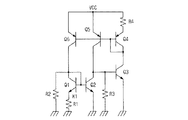
以下、本発明における実施の形態を、基準電流回路の実施の形態と基準電圧回路の実施の形態とに分けて説明する。先ず、図面を用いて本発明における基準電流回路の実施の形態を説明する。図1は、本発明の請求項1に記載されたバイポーラ基準電流回路の一実施例を示す回路図である。トランジスタQ1、Q2、抵抗R1はバイポーラ永田カレントミラー回路を構成しており、同様に、トランジスタQ4、Q5(、Q6)、抵抗R4はバイポーラ永田カレントミラー回路を構成している。ここでは、カレントソースを構成しているトランジスタQ5、Q6により、トランジスタQ1、Q2、抵抗R1はバイポーラ自己バイアス永田基準電流回路となっている。また、トランジスタQ4、Q5(、Q6)、抵抗R2からなるバイポーラ永田カレントミラー回路は駆動するトランジスタQ3の電流が増加するとトランジスタQ5、Q6に流れる電流が減少するように回路定数が設定されている。これにより、バイポーラ自己バイアス永田基準電流回路内では負帰還電流ループが構成され、回路が安定動作する。尚、特開平7-200086号公報に記載されたバイポーラ自己バイアス永田基準電流回路では回路内では正帰還電流ループが構成され、回路が動作しない。
【0030】
図2に、トランジスタQ1、Q2、抵抗R1からなるバイポーラ永田カレントミラー回路(図1)の入出力特性を示す。同図は、横軸に入力電流IC1、縦軸に出力電流IC2がとってある。バイポーラ永田カレントミラー回路の特徴は、入力電流(基準電流)IC1に対し出力電流(ミラー電流)IC2が単調に増加する領域と、ピーク点と、入力電流(基準電流)IC1に対し出力電流(ミラー電流)IC2が単調に減少する領域とがある。ピーク点は、入力電流(基準電流)がIC1=VT/R1のときに、出力電流(ミラー電流)がIC2=K1VT/eR1となっている。トランジスタの直流電流増幅率は十分に1に近いものとして、ベース電流を無視すれば、バイポーラ永田カレントミラー回路においては、(1)式により、
VBE1=VTln(IC1/IS) (20)
VBE2=VTln{IC2/(K1IS)} (21)
VBE1=VBE2+R1IC1 (22)
なる関係がある。
【0031】
ここで、(20)式から(22)式を解くと、バイポーラ永田カレントミラー回路の入力電流と出力電流の関係は、
IC2=K1IC1exp{−R1IC1/(VT)} (23)
と表され、ピーク点はR1IC1=VTの時にIC2=K1IC1/eとなっている。但し、e=2.7183である。したがって、K1=eの時にIC2=IC1となる。ここで、トランジスタQ3はトランジスタQ4を駆動しており、トランジスタQ4はトランジスタQ5、Q6、抵抗R4とで、入力電流(基準電流)に対し出力電流(ミラー電流)が単調に減少する領域で動作するバイポーラ永田カレントミラー回路を構成しており、トランジスタQ1とトランジスタQ2はそれぞれトランジスタQ6、Q5で駆動されているから、バイポーラ自己バイアス永田基準電流回路となっており、トランジスタQ5、Q6のエミッタ面積比を1:K2とすると、
IC1=K2IC2 (24)
となる。但し、トランジスタQ4を単位トランジスタとすると、トランジスタQ5のエミッタ面積比は単位トランジスタのK3倍であり、トランジスタQ6のエミッタ面積比は単位トランジスタのK2K3倍である。また、バイポーラ永田カレントミラー回路が単純減少領域で動作しているためには、K3>e(=2.7183)である必要がある。
【0032】
したがって、
ΔVBE=VBE1−VBE2=VTln(IC1/IS)−VTln{IC2/(K1IS)}=VTln(K1IC1/IC2)=VTln(K1K2)=R1IC1 (25)
が成り立つから、
I0=IC1=(VT/R1)ln(K1K2) (26)
と求められる。ここで、K1、K2 は温度特性を持たない定数であり、上述したように、熱電圧VT は、VT=kT/qと表され、3333ppm/℃の温度特性となっている。したがって、抵抗R1の温度特性が熱電圧VT の温度特性よりも小さく、温度に対して1次特性であれば、カレントミラー回路を介して出力される基準電流回路の出力電流I0(=IC1)は温度に比例することになり、PTATカレントソース回路となることがわかる。
【0033】
また、トランジスタQ1、Q3に流れる電流がいずれも等しくなるように、エミッタ面積比K1、K2、K3を設定し、抵抗R1、R4の値を設定することで、トランジスタQ1、Q3のベース電圧がほぼ等しくなり、トランジスタQ1 Q2のコレクタ電圧は固定され等しく設定される。このことにより、トランジスタQ1、Q2のアーリー電圧の影響が現れず、トランジスタQ5、Q6のコレクタ電圧が変化してアーリー電圧の影響が現れても所望の電流ミラー比は変化しないから、電源電圧変動に対して変化の少ない高精度の電流出力が得られる。また、トランジスタQ1、Q3に流れる電流が等しくない場合にでも、少なくとも、トランジスタQ1、Q3のベース電圧によりトランジスタQ1、Q2のコレクタ電圧が固定され、変動幅が少ないから、トランジスタQ1、Q2のアーリー電圧(チャネル長変調)の影響はほとんど現れない。
【0034】
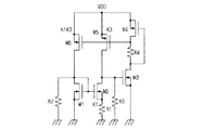
次に、図3は本発明の請求項1に記載されたCMOS基準電流回路の一実施例を示す回路図である。トランジスタM1、M2、抵抗R1は永田カレントミラー回路を構成しており、同様に、トランジスタM4、M5(、M6)、抵抗R4は永田カレントミラー回路を構成している。ここでは、カレントソースを構成しているトランジスタM5、M6により、トランジスタM1、M2、抵抗R1は自己バイアス永田基準電流回路となっている。また、トランジスタM4、M5(、M6)、抵抗R2からなるMOS永田カレントミラー回路は駆動するトランジスタM3の電流が増加すると、トランジスタM5、M6に流れる電流が減少するように回路定数が設定されている。これにより、CMOS自己バイアス永田基準電流回路内では負帰還電流ループが構成され、回路が安定動作する。なお、特開平7-200086号公報に記載されたCMOS自己バイアス永田基準電流回路では回路内では正帰還電流ループが構成され、回路が動作しない。
【0035】
図3において、トランジスタM1を単位トランジスタ、トランジスタM2のゲート幅W/ゲート長Lの比(W/L)を単位トランジスタのK1倍(K1>1)とする。図3に示すMOS永田カレントミラー回路においては素子の整合性は良いものとし、チャネル長変調と基板効果を無視し、MOSトランジスタのドレイン電流とゲート―ソース間電圧の関係は2乗則に従うものとすると、MOSトランジスタM1のドレイン電流は、
ID1=β(VGS1−VTH)2 (27)
と表される。ここで、βはトランスコンダクタンス・パラメータであり、β=μ(COX/2)(W/L) と表される。ただし、μはキャリアの実効モビリティ、COX は単位面積当たりのゲート酸化膜容量、W、Lはそれぞれゲート幅、ゲート長である。
【0036】
MOSトランジスタM2のドレイン電流は、
ID2=K1β(VGS2−VTH)2 (28)
と表される。また、
VGS1=VGS2+R1ID1 (29)
なる関係がある。
ここで、(27)式から(29)式を解くと、MOS永田カレントミラー回路の入力電流と出力電流の関係は、
【数1】

【0037】
図4に、トランジスタM1、M2、抵抗R1からなるMOS永田カレントミラー回路の入出力特性を示す。同図は、横軸に入力電流ID1、縦軸に出力電流ID2がとってある。MOS永田カレントミラー回路の特徴は、バイポーラ永田カレントミラー回路の場合と同様に、入力電流(基準電流)ID1に対し出力電流(ミラー電流)ID2が単調に増加する領域と、ピーク点と、入力電流(基準電流)ID1に対し出力電流(ミラー電流)ID2が単調に減少する領域とがある。ピーク点は、入力電流(基準電流)がID1=1/(4R1 2β)の時に出力電流(ミラー電流)がID2=K1/16R1 2βとなっている。通常は、ID1=1/(4R1 2β)の時にID2=K1ID1/4である。したがって、K1=4の時にID2=ID1となる。
【0038】
ここで、トランジスタM3はトランジスタM4を駆動しており、トランジスタM4はトランジスタM5、M6、抵抗R4とで、入力電流(基準電流)に対し出力電流(ミラー電流)が単調に減少する領域で動作するMOS永田カレントミラー回路を構成しており、トランジスタM1とトランジスタM2はそれぞれトランジスタM6、M5で駆動されているから、MOS自己バイアス永田基準電流回路となっており、トランジスタM5、M6のエミッタ面積比を1:K2とすると、
ID1=K2ID2 (31)
となる。但し、トランジスタM4を単位トランジスタとすると、トランジスタM5のゲート幅W/ゲート長Lの比(W/L)は単位トランジスタのK3倍であり、トランジスタM6のゲート幅W/ゲート長Lの比(W/L)は単位トランジスタのK2K3倍である。また、MOS永田カレントミラー回路が単純減少領域で動作しているためには、K3>4である必要がある。
【0039】
したがって、
ΔVGS=VGS1−VGS2=R1ID1 (32)
となり、(29)式から(32)式を解くと、
【数2】
【数3】
【数4】
【0040】
図5は、図3の回路における1/β(トランスコンダクタンス・パラメータの逆数)の温度特性の計算値を示している。1/βの温度特性は常温では5000ppm/℃となっている。これはバイポーラトランジスタの熱電圧VTの温度特性3333ppm/℃の1.5倍に当たる。すなわち、CMOS基準電流回路の出力電流IREFは、
【数5】
【0041】
ここで、トランジスタM1、M3に流れる電流がいずれも等しくなるように、トランジスタサイズ比(ゲート幅W/ゲート長Lの比(W/L)の比(W/L)/(W/L))K1、K2、K3を設定し、抵抗R1、R4の値を設定することで、トランジスタM1、M3のゲート電圧がほぼ等しくでき、したがって、トランジスタM1、M2のドレイン電圧は固定され等しく設定される。このことにより、トランジスタM1、M2のアーリー電圧(チャネル長変調)の影響が現れず、トランジスタM5、M6のドレイン電圧が変化してアーリー電圧(チャネル長変調)の影響が現れても所望の電流ミラー比は変化しないから、電源電圧変動に対して変化の少ない高精度の電流出力が得られる。また、トランジスタM1、M3に流れる電流が等しくない場合にでも、少なくとも、トランジスタM1、M3のゲート電圧によりトランジスタM1、M2のドレイン電圧が固定され、変動幅が少ないから、トランジスタM1、M2のアーリー電圧(チャネル長変調)の影響はほとんど現れない。
【0042】
図6は、本発明の請求項1に記載されたCMOS基準電流回路の他の実施例を示す回路図である。トランジスタM1、M2、抵抗R1はMOS逆ワイドラーカレントミラー回路を構成しており、従来技術で説明したのと同様に、負帰還電流ループが構成され、設定された動作点で安定に動作するから、MOS逆ワイドラーカレントミラー回路を自己バイアス化してCMOS基準電流回路が実現される。図6において、トランジスタM2を単位トランジスタ、トランジスタM1のゲート幅W/ゲート長Lの比(W/L)を単位トランジスタのK1倍(K1>1)とすると、MOSトランジスタM1、M2のドレイン電流は、
ID1=K1β(VGS1−VTH)2 (37)
ID2=β(VGS2−VTH)2 (38)
と表される。また、
VGS2=VGS1+R1ID1 (39)
なる関係がある。
【0043】
ここで、(37)式から(39)式を解くと、
【数6】
図7に、MOS逆ワイドラーカレントミラー回路の入出力特性を示す。同図は、横軸に入力電流ID1、縦軸に出力電流ID2がとってあり、K1=1及びK1=4をパラメータとした特性を示している。
【0044】
ここで、トランジスタM3はトランジスタM4を駆動しており、トランジスタM4はトランジスタM5、M6とでカレントミラー回路を構成しており、トランジスタM1とトランジスタM2はそれぞれトランジスタM6、M5で駆動されているから、MOS自己バイアス逆ワイドラー基準電流回路となっており、トランジスタM6、M5のゲート幅W/ゲート長Lの比(W/L)の比(W/L)6:(W/L)5を1:K2とすると、
K2ID1=ID2 (41)
となる。また、
ΔVGS=VGS2−VGS1=R1ID1 (42)
ここで、(37)式から(42)式を解くと、
【数7】
【0045】
ここで、K1、K2 は温度特性を持たない定数である。一方、MOSトランジスタではモビリティμが温度特性を持つから、トランスコンダクタンス・パラメータβの温度依存性は(31)式で表され、CMOS基準電流回路の出力電流IREFは、
【数8】
【0046】
したがって、抵抗R2の温度特性が5000ppm/℃以下で温度に対して1次特性であればドレイン電流ID1が正の温度特性を持ち、カレントミラー回路を介して出力される基準電流回路の出力電流I0は温度に比例することになり、PTATカレントソース回路となることがわかる。ここで、K2=1として、トランジスタM2、M3、M4、M5、M6をそれぞれ単位トランジスタとすることでトランジスタM2、M3のゲート電圧が等しくなるようにすることができ、トランジスタM5、M6のドレイン電圧は固定され等しく設定される。このことにより、トランジスタM1、M2のアーリー電圧(チャネル長変調)の影響が現れず、トランジスタM5、M6のドレイン電圧が変化してアーリー電圧(チャネル長変調)の影響が現れても所望の電流ミラー比は変化しないから、電源電圧変動に対して変化の少ない高精度の電流出力が得られる。K2≠1の場合でも、少なくとも、トランジスタM2、M3のゲート電圧によりトランジスタM1、M2のドレイン電圧が固定され、変動幅が少ないから、トランジスタM1、M2のアーリー電圧(チャネル長変調)の影響はほとんど現れない。
【0047】
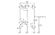
次に、図8は本発明の請求項1に記載されたバイポーラ基準電流回路の他の実施例を示す回路図である。トランジスタQ1、Q2、抵抗R1はバイポーラワイドラーカレントミラー回路を構成しており、同様に、トランジスタQ4、Q5(、Q6)、抵抗R4はバイポーラ永田カレントミラー回路を構成している。ここでは、カレントソースを構成しているトランジスタQ5、Q6により、トランジスタQ1、Q2、抵抗R1はバイポーラ自己バイアスワイドラー基準電流回路となっている。また、トランジスタQ4、Q5(、Q6)、抵抗R4からなるバイポーラ永田カレントミラー回路は駆動するトランジスタQ3の電流が増加するとトランジスタQ5、Q6に流れる電流が減少するように回路定数が設定されている。これにより、バイポーラ自己バイアス永田基準電流回路内では負帰還電流ループが構成され、回路が安定動作する。なお、特開平7-200086号公報に記載されたバイポーラ自己バイアスワイドラー基準電流回路では回路内では正帰還電流ループが構成され、回路が動作しない。
【0048】
トランジスタの直流電流増幅率は十分に1に近いものとして、ベース電流を無視すれば、バイポーラワイドラーカレントミラー回路においては、(1)式により、
VBE1=VTln(IC1/IS) (45)
VBE2=VTln{IC2/(K1IS)} (46)
VBE1=VBE2+R1IC2 (47)
なる関係がある。
ここで、(45)式から(47)式を解くと、バイポーラワイドラーカレントミラー回路の入力電流と出力電流の関係は、
IC1=(IC2/K1)exp(R1IC2/VT) (48)
と表され、バイポーラワイドラーカレントミラー回路の入力電流と出力電流の関係はバイポーラ逆ワイドラーカレントミラー回路の入力電流と出力電流の関係を丁度入力と出力を入れ替えた関係になっている。図9に、トランジスタQ1、Q2、抵抗R1からなるバイポーラワイドラーカレントミラー回路の入出力特性を示す。
【0049】
ここで、トランジスタQ3はトランジスタQ4を駆動しており、トランジスタQ4はトランジスタQ5、Q6、抵抗R4とで、入力電流(基準電流)に対し出力電流(ミラー電流)が単調に減少する領域で動作するバイポーラ永田カレントミラー回路を構成しており、トランジスタQ1とトランジスタQ2はそれぞれトランジスタQ6、Q5で駆動されているから、バイポーラ自己バイアスワイドラー基準電流回路となっており、トランジスタQ5、Q6のエミッタ面積比を1:K2とすると、
IC1=K2IC2 (49)
となる。ただし、トランジスタQ4を単位トランジスタとすると、トランジスタQ5のエミッタ面積比は単位トランジスタのK3倍であり、トランジスタQ6のエミッタ面積比は単位トランジスタのK2K3倍である。また、バイポーラ永田カレントミラー回路が単純減少領域で動作しているためには、K3>e(=2.7183)である必要がある。
【0050】
また、
ΔVBE=VBE1−VBE2=VTln(IC1/IS)−VTln{IC2/(K1IS)}=VTln(K1IC1/IC2)=VTln(K1K2)=R1IC2 (50)
が成り立つから、
I0=IC1={VT/(R1K2)}ln(K1K2) (51)
と求められる。ここで、K1、K2 は温度特性を持たない定数であり、上述したように、熱電圧VT は、VT=kT/qと表され、3333ppm/℃の温度特性となっている。したがって、抵抗R1の温度特性が熱電圧VT の温度特性よりも小さく、温度に対して1次特性であれば、カレントミラー回路を介して出力される基準電流回路の出力電流I0(=IC1)は温度に比例することになり、PTATカレントソース回路となることがわかる。
【0051】
ここで、トランジスタQ1、Q3に流れる電流がいずれも等しくなるように、エミッタ面積比K1、K2、K3を設定し、抵抗R1、R4の値を設定することで、トランジスタQ1、Q3のベース電圧がほぼ等しくなり、トランジスタQ1、Q2のコレクタ電圧は固定され等しく設定される。このことにより、トランジスタQ1、Q2のアーリー電圧の影響が現れず、トランジスタQ5、Q6のコレクタ電圧が変化してアーリー電圧の影響が現れても所望の電流ミラー比は変化しないから、電源電圧変動に対して変化の少ない高精度の電流出力が得られる。また、トランジスタQ1、Q3に流れる電流が等しくない場合にでも、少なくとも、トランジスタQ1、Q3のベース電圧によりトランジスタQ1、Q2のコレクタ電圧が固定され、変動幅が少ないから、トランジスタQ1、Q2のアーリー電圧(チャネル長変調)の影響はほとんど現れない。
【0052】
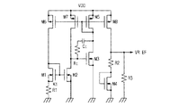
次に、図10は本発明の請求項1に記載されたCMOS基準電流回路の他の実施例を示す回路図である。トランジスタM1、M2、抵抗R1はMOSワイドラーカレントミラー回路を構成しており、同様に、トランジスタM4、M5(、M6)、抵抗R4はMOS永田カレントミラー回路を構成している。ここでは、カレントソースを構成しているトランジスタM5、M6により、トランジスタM1、M2、抵抗R1はCMOS自己バイアスワイドラー基準電流回路となっている。また、トランジスタM4、M5(、M6)、抵抗R4からなるMOS永田カレントミラー回路は駆動するトランジスタM3の電流が増加するとトランジスタM5、M6に流れる電流が減少するように回路定数が設定されている。これにより、CMOS自己バイアスワイドラー基準電流回路内では負帰還電流ループが構成され、回路が安定動作する。なお、特開平7-200086号公報に記載されたCMOS自己バイアスワイドラー基準電流回路では回路内では正帰還電流ループが構成され、回路が動作しない。尚、図11に、トランジスタM1、M2、抵抗R1からなるMOSワイドラーカレントミラー回路の入出力特性を示す。
【0053】
図10において、トランジスタM1を単位トランジスタ、トランジスタM2のゲート幅W/ゲート長Lの比(W/L)を単位トランジスタのK1倍(K1>1)とする。図10に示すMOSワイドラーカレントミラー回路においては素子の整合性は良いものとし、チャネル長変調と基板効果を無視し、MOSトランジスタのドレイン電流とゲート―ソース間電圧の関係は2乗則に従うものとすると、MOSトランジスタM1、M2のドレイン電流は、
ID1=β(VGS1−VTH)2 (52)
ID2=K1β(VGS2−VTH)2 (53)
と表される。また、
VGS1=VGS2+R1ID2 (54)
なる関係がある。
ここで、(52)式から(54)式を解くと、MOSワイドラーカレントミラー回路の入力電流と出力電流の関係は、
【数9】
【0054】
ここで、トランジスタM3はトランジスタM4を駆動しており、トランジスタM4はトランジスタM5、M6、抵抗R4とで、入力電流(基準電流)に対し出力電流(ミラー電流)が単調に減少する領域で動作するMOS永田カレントミラー回路を構成しており、トランジスタM1とトランジスタM2はそれぞれトランジスタM6、M5で駆動されているから、MOS自己バイアスワイドラー基準電流回路となっており、トランジスタM5、M6のエミッタ面積比を1:K2とすると、
ID1=K2ID2 (56)
となる。また、
ΔVGS=VGS1−VGS2=R1ID2 (57)
となり、(52)式から(57)式を解くと、
【数10】
【0055】
ここで、K1、K2 は温度特性を持たない定数である。一方、MOSトランジスタではモビリティμが温度特性を持つから、トランスコンダクタンス・パラメータβの温度依存性は(31)式で表され、CMOS基準電流回路の出力電流IRE Fは
【数11】
【0056】
このことにより、トランジスタM1、M2のアーリー電圧(チャネル長変調)の影響が現れず、トランジスタM5、M6のドレイン電圧が変化してアーリー電圧(チャネル長変調)の影響が現れても所望の電流ミラー比は変化しないから、電源電圧変動に対して変化の少ない高精度の電流出力が得られる。また、トランジスタM1、M3に流れる電流が等しくない場合にでも、少なくとも、トランジスタM1、M3のゲート電圧によりトランジスタM1、M2のドレイン電圧が固定され、変動幅が少ないから、トランジスタM1、M2のアーリー電圧(チャネル長変調)の影響はほとんど現れない。
【0057】
以上は正の温度特性を持つ電流を出力する基準電流回路(PTATカレントソース)について説明した。これらの回路では、カレントミラー回路を構成する2つの出力トランジスタのコレクタ(ドレイン)電圧が等しいか、ほぼ等しくなるように回路を構成している。少なくとも、カレントミラー回路を構成する2つの出力トランジスタのコレクタ(ドレイン)電圧の温度特性は負の特性を持つ。このドレイン電圧の温度特性を利用して負の温度特性を持つ電流IIPTATを得、PTATカレントソースから得られる正の温度特性を持つ電流IPTATとを重み付け加算することで任意の温度特性を持つ電流を出力する基準電流回路が実現できることを示す。
【0058】
図12は、本発明の請求項2に記載されたバイポーラ基準電流回路の一実施例を示す回路図であり、任意の温度特性を持つ電流を出力する。図12において、トランジスタQ1、Q2、抵抗R1はバイポーラ逆ワイドラーカレントミラー回路を構成しており、トランジスタQ4、Q5(、Q6)、抵抗R4はバイポーラ逆ワイドラーカレントミラー回路を構成している。ここで、抵抗R2とR3に流れる電流比がトランジスタQ6、Q5からなるカレントミラー回路の電流比と等しいならば、トランジスタQ1、Q2(、Q3)、Q5、Q6、抵抗R1はバイポーラ自己バイアス逆ワイドラー基準電流回路を構成する。このためには、抵抗R2の端子電圧V1(=VBE2)と抵抗R3の端子電圧V2(=VBE3)が等しくなるように設定し、抵抗R2の抵抗値と抵抗R3の抵抗値の比をカレントミラー回路の電流比の逆数に設定すれば良い。
【0059】
トランジスタの直流電流増幅率は十分に1に近いものとして、ベース電流を無視すれば、(1)式により、
VBE1=VTln{IC1/(K1IS)} (60)
VBE2=VTln(IC2/IS) (61)
VBE2=VBE1+R1IC1 (62)
なる関係がある。
次に、トランジスタQ1と抵抗R2、トランジスタQ2と抵抗R3をミラー比が1:1のカレントミラーで駆動すると、
IC1+V1/R2=IC2+V2/R3 (63)
となる。ここで、トランジスタQ4、Q5(、Q6)、抵抗R4はバイポーラ逆ワイドラーカレントミラー回路を構成しており、トランジスタQ5、Q6は単位トランジスタであり、トランジスタQ4のエミッタ面積比は単位トランジスタのK3倍であり、抵抗R4を設定することで、IC3=IC4=IC2となるようにすれば、V1=V2(∴VBE2=VBE3)となり、R3=R2ならば、
IC1=IC2 (64)
が成り立つ。したがって、
ΔVBE=VBE2−VBE1=VTln(IC1/IS)−VTln{IC2/(K1IS)}=VTln{IC1/(IC2/K1)}=VTln(K1K2)=R1IC1 (65)
と求められる。ここで、K1、K2 は温度特性を持たない定数であり、上述したように、VT=kT/qと表され、熱電圧VTは3333ppm/℃の温度特性となっている。したがって、ΔVBE は温度に比例する。
【0060】
バイポーラ基準電流回路の出力電流IREFは
IREF=IC2+V2/R3=ΔVBE/R1+VBE3/R3=(VT/R1)ln(K1K2)+VBEE2/R3 (66)
と求められる。すなわち、バイポーラ基準電流回路の出力電流IREFは負の温度特性を持つベース・エミッタ電圧VBEと正の温度特性を持つΔVBEの重み付け加算式で表される。したがって、重み付けを変ることで2つの基準電圧の温度特性を上述したように、任意に設定できる。具体的には、エミッタ面積比、あるいは、カレントミラー比と各抵抗比を設定すれば良い。例えば、バイポーラ基準電流回路の出力電流IREFを抵抗R5で電圧変換することで、出力電圧VREFは
VREF=R5IREF=(R5/R1)VTln(K1K2)+(R5/R3)VBE2=(R5/R3){VBE2+(R3/R1)VTln(K1K2)} (67)
となる。
【0061】
ここで、熱電圧VTは3333ppm/℃の正の温度特性を持ち、トランジスタQ2、Q3のベース・エミッタ電圧VBE2、VBE3はおよそ−1.9mV/℃の負の温度特性を持ち、かつ抵抗比(R5/R1)、(R5/R3)は温度特性が相殺されて零であり、ln(K1K2)も温度特性を持たないから、バイポーラ基準電流回路の出力電流を抵抗で電圧変換して得られる出力電圧VREFは、熱電圧VTの持つ3333ppm/℃の正の温度特性とトランジスタQ2のベース・エミッタ電圧VBE2の持つ負の温度特性、およそ−1.9mV/℃、で決定される。例えば、バイポーラ基準電流回路の出力電流を抵抗で電圧変換して得られるVREFの温度特性を零とするためには、常温でのトランジスタQ2のベース・エミッタ電圧VB出力電圧E2(=VBE3)を630mVとすると、熱電圧VTは常温で25.6mVであるから、(R3/R1)ln(K1K2)=22.3と求められる。したがって、{VBE2+(R3/R1)VTln(K1K2)}=1.2Vとなる。こうして得られる温度特性が零の出力電圧VREFは抵抗R5と抵抗R3の比(R5/R3)を任意に設定することで任意の電圧値に設定できる。
【0062】
(R5/R3)<1に設定する場合では、例えば、0.7Vに設定する場合を考えると、0.9V程度から動作可能となる。あるいは、電源電圧に余裕があれば、(R5/R3)>1に設定すれば、VREF>1.2Vでの温度特性が零である基準電圧が得られる。具体的には、(R5/R3)=1.25に設定すればVREF=1.5V、(R5/R3)=5/3に設定すればVREF=2.0Vが得られる。以上の説明により、抵抗R5をR5>R3に設定し、抵抗R5に任意に(n−1)個のタップを設けて出力端子とすれば、温度特性を持たない任意の異なる電圧値のn個の基準電圧が得られる。
【0063】
次に、図13は本発明の請求項2に記載されたCMOS基準電流回路の一実施例を示す回路図であり、任意の温度特性を持つ電流を出力する。トランジスタM1、M2、抵抗R1はMOS逆ワイドラーカレントミラー回路を構成しており、トランジスタM4、M5(、M6)、抵抗R4はMOS逆ワイドラーカレントミラー回路を構成している。ここで、抵抗R2とR3に流れる電流比がトランジスタM6、M5からなるカレントミラー回路の電流比と等しいならば、トランジスタM1、M2(、M3)、M5、M6、抵抗R1はバイポーラ自己バイアス逆ワイドラー基準電流回路を構成する。このためには、抵抗R2の端子電圧V1(=VGS2)と抵抗R3の端子電圧V2(=VGS3)が等しくなるように設定し、抵抗R2の抵抗値と抵抗R3の抵抗値の比をカレントミラー回路の電流比の逆数に設定すれば良い。図13において、トランジスタM2を単位トランジスタ、トランジスタM1のゲート幅W/ゲート長Lの比(W/L)を単位トランジスタのK1倍(K1>1)とする。
【0064】
素子の整合性は良いものとすると、MOSトランジスタM1、M2のドレイン電流は、
ID1=K1β(VGS1−VTH)2 (68)
ID2=β(VGS2−VTH)2 (69)
と表される。また、
ΔVGS=VGS2−VGS1=R1ID1 (70)
なる関係がある。
次に、トランジスタM1と抵抗R2、トランジスタM2と抵抗R3をミラー比が1:1のカレントミラーで駆動すると、
ID1+V1/R2=ID2+V2/R3 (71)
となる。ここで、トランジスタM4、M5(、M6)、抵抗R4はMOS逆ワイドラーカレントミラー回路を構成しており、トランジスタM5、M6は単位トランジスタであり、トランジスタM4のゲート幅W/ゲート長Lの比(W/L)は単位トランジスタのK3倍であり、抵抗R4を設定することで、ID3=ID4=ID2となるようにすれば、V1=V2(∴VGS2=VGS3)となり、R3=R2ならば、
ID1=ID2 (72)
が成り立つ。
【0065】
したがって、(68)式から(72)式を解くと、
【数12】
【0066】
すなわち、MOS基準電圧回路の出力電流IREFは
IREF=ID2+V2/R3=ID1+VGS2/R3 (74)
と求められる。
一方、(69)式より、
【数13】
【数14】
VTH=VTH0−α(T−T0) (77)
と表され、αは低スレッショルド電圧のCMOSプロセスにおいてはおよそ2.3mV/℃である。したがって、MOS基準電圧回路の出力電流IREFは負の温度特性を持つスレッショルド電圧VTHの項と正の温度特性を持つ1/βの項の重み付け加算式で表される。したがって、重み付けを変ることで基準電流の温度特性を任意に設定できる。例えば、MOS基準電流回路の出力電流IREFを抵抗R5で電圧変換することで、出力電圧VREFは、
VREF=R5IREF
【数15】
【0067】
(78)式の右辺は、負の温度特性を持つスレッショルド電圧VTHと正の温度特性を持つトランスコンダクタンス・パラメータ(モビリティ)の逆数に起因する電圧値の重み付け加算式で表される。したがって、重み付けを変ることで、MOS基準電圧回路の出力電圧VREFの温度特性を上述したように、任意に設定できる。具体的には、(W/L)/(W/L)比、あるいは、カレントミラー比と抵抗の値、および、各抵抗比を設定すれば良い。ここで、トランスコンダクタンス・パラメータβの逆数1/βの温度特性はほぼ温度に比例し常温では5000ppm/℃となっており、トランジスタM2のスレッショルド電圧VTHはおよそ−2.3mV/℃の負の温度特性を持ち、かつ抵抗比(R5/R1)、(R5/R3)は温度特性が相殺されて零であり、√K1も温度特性を持たないから、MOS基準電圧回路の出力電圧VREFは5000ppm/℃の正の温度特性とトランジスタM2のスレッショルド電圧VTHの負の温度特性、およそ−2.3mV/℃、で決定される。例えば、VTH0=0.7Vとすれば、
【数16】
VREF=(R5/R3)(0.46+0.7)=1.16 (R5/R3)V (80)
となり、電圧1.16Vは温度特性を持たない。したがって、(R5/R3)は温度特性が相殺されて零であるから、出力される基準電圧VREFは温度特性を持たない。
【0068】
ここで、抵抗R5と抵抗R3の比 (R5/R3)は任意に設定できる。例えば、(R5/R3)<1に設定すれば、低電圧で動作可能となる。具体的には、R5/R3=0.69に設定すればVREF=0.8Vとなり、電源電圧1.0V程度から動作可能となる。また、(R5/R3)>1に設定することもできる。例えば、R5/R3=1.72に設定すればVREF=2.0Vとなり、電源電圧2.2V程度から動作可能となる。さらに、抵抗R5に3つのタップを設けて抵抗値を4等分すれば、いずれも温度特性を持たない4つの基準電圧、VREF1=0.5V、VREF2=1.0V、VREF3=1.5V、VREF4=2.0Vが得られる。
【0069】
さらに、図14は本発明の請求項2に記載されたバイポーラ基準電流回路の他の実施例を示す回路図であり、任意の温度特性を持つ電流を出力する。図14において、トランジスタQ1、Q2、抵抗R1はバイポーラ永田ワイドラーカレントミラー回路を構成しており、トランジスタQ4、Q5(、Q6)、抵抗R4からなるバイポーラ永田カレントミラー回路は駆動するトランジスタQ3の電流が増加するとトランジスタQ5、Q6に流れる電流が減少するように回路定数が設定されている。これにより、回路内では負帰還電流ループが構成され、回路が安定動作する。ここで、抵抗R2とR3に流れる電流比がトランジスタQ6、Q5からなるカレントミラー回路の電流比と等しいならば、トランジスタQ1、Q2(、Q3)、Q5、Q6、抵抗R1はバイポーラ自己バイアス永田基準電流回路を構成する。このためには、抵抗R2の端子電圧V1(=VBE2)と抵抗R3の端子電圧V2(=VBE3)が等しくなるようにK1、K2、K3、抵抗R1、R4を設定し、抵抗R2の抵抗値と抵抗R3の抵抗値の比をカレントミラー回路の電流比の逆数に設定すれば良い。
【0070】
トランジスタの直流電流増幅率は十分に1に近いものとして、ベース電流を無視すれば、(1)式により、
VBE1=VTln(IC1/IS) (81)
VBE2=VTln{IC2/(K1IS)} (82)
VBE1=VBE2+R1IC1 (83)
なる関係がある。
【0071】
次に、トランジスタQ1と抵抗R2、トランジスタQ2と抵抗R3をミラー比がK2:1のカレントミラーで駆動すると、
IC1+V1/R2=K2(IC2+V2/R3) (84)
となる。ここで、トランジスタQ4、Q5(、Q6)、抵抗R4はバイポーラ永田カレントミラー回路を構成しており、トランジスタQ5、Q6は単位トランジスタであり、トランジスタQ4のエミッタ面積比は単位トランジスタのK3倍であり、抵抗R4を設定することで、IC1=IC3となるようにすれば、V1=V2(∴VBE2=VBE3)となり、R3/R2=K2ならば、
IC1=K2IC2 (85)
が成り立つ。したがって、
ΔVBE=VBE1−VBE2=VTln(IC1/IS)−VTln{IC2/(K1IS)}=VTln{IC1/(IC2/K1)}=VTln(K1K2)=R1IC1 (86)
と求められる。ここで、K1、K2 は温度特性を持たない定数であり、上述したように、VT=kT/qと表され、熱電圧VTは3333ppm/℃の温度特性となっている。したがって、ΔVBEは温度に比例する。
【0072】
バイポーラ基準電圧回路の出力電流IREFは
IREF=IC2+V2/R3=ΔVBE/(K2R1)+VBE3/R3={VT/(K2R1)}ln(K1K2)+VBE1/R3 (87)
と求められる。すなわち、バイポーラ基準電流回路の出力電流IREFは負の温度特性を持つベース・エミッタ電圧VBEと正の温度特性を持つΔVBEの重み付け加算式で表される。したがって、重み付けを変ることで2つの基準電圧の温度特性を上述したように、任意に設定できる。具体的には、エミッタ面積比、あるいは、カレントミラー比と各抵抗比を設定すれば良い。例えば、バイポーラ基準電流回路の出力電流IREFを抵抗R5で電圧変換することで、出力電圧VREFは、
VREF=R5IREF={R5/(K2R1)}VTln(K1K2)+(R5/R3)VBE1=(R5/R3)[{R3/(K2R1)}VTln(K1K2)+VBE1] (88)
となる。
【0073】
ここで、熱電圧VTは3333ppm/℃の正の温度特性を持ち、トランジスタQ2、Q3のベース・エミッタ電圧VBE2、VBE3はおよそ−1.9mV/℃の負の温度特性を持ち、かつ抵抗比(R5/R1)、(R5/R3)は温度特性が相殺されて零であり、K2、ln(K1K2)も温度特性を持たないから、バイポーラ基準電流回路の出力電流を抵抗で電圧変換して得られる出力電圧VREFは、熱電圧VTの持つ3333ppm/℃の正の温度特性とトランジスタQ1のベース・エミッタ電圧VBE1の持つ負の温度特性、およそ−1.9mV/℃、で決定される。例えば、バイポーラ基準電流回路の出力電流を抵抗で電圧変換して得られる出力電圧VREFの温度特性を零とするためには、常温でのトランジスタQ1のベース・エミッタ電圧VBE1、(=VBE3)を630mVとすると、熱電圧VT は常温で25.6mVであるから、(R3/K2R1)ln(K1K2)=22.3と求められる。したがって、{R3/(K2R1)}VTln(K1K2)+VBE1=1.2Vとなる。
【0074】
こうして得られる温度特性が零の出力電圧VREFは抵抗R5と抵抗R3の比(R5/R3)を任意に設定することで任意の電圧値に設定できる。(R5/R3)<1に設定する場合では、例えば、0.7Vに設定する場合を考えると、0.9V程度から動作可能となる。あるいは、電源電圧に余裕があれば、(R5/R3)>1に設定すれば、VREF>1.2Vでの温度特性が零である基準電圧が得られる。具体的には、(R5/R3)=1.25に設定すればVREF=1.5V、(R5/R3)=5/3に設定すればVREF=2.0Vが得られる。以上の説明により、抵抗R5をR5>R3に設定し、抵抗R5に任意に(n−1)個のタップを設けて出力端子とすれば、温度特性を持たない任意の異なる電圧値のn個の基準電圧が得られる。
【0075】
さらに、図15は本発明の請求項2に記載されたCMOS基準電流回路の他の実施例を示す回路図であり、任意の温度特性を持つ電流を出力する。トランジスタM1、M2、抵抗R1はMOS永田カレントミラー回路を構成しており、トランジスタM4、M5(、M6)、抵抗R4からなるMOS永田カレントミラー回路は駆動するトランジスタM3の電流が増加するとトランジスタM5、M6に流れる電流が減少するように回路定数が設定されている。これにより、回路内では負帰還電流ループが構成され、回路が安定動作する。ここで、抵抗R2とR3に流れる電流比がトランジスタM6、M5からなるカレントミラー回路の電流比と等しいならば、トランジスタM1、M2(、M3)、M5、M6、抵抗R1はMOS自己バイアス永田基準電流回路を構成する。このためには、抵抗R2の端子電圧V1(=VGS1)と抵抗R3の端子電圧V2(=VGS3)が等しくなるようにK1、K2、K3、抵抗R1、R2を設定し、抵抗R2の抵抗値と抵抗R3の抵抗値の比をカレントミラー回路の電流比の逆数に設定すれば良い。図15において、トランジスタM2を単位トランジスタ、トランジスタM1のゲート幅W/ゲート長Lの比(W/L)を単位トランジスタのK1倍(K1>1)とする。
【0076】
素子の整合性は良いものとすると、MOSトランジスタM1、M2のドレイン電流は、
ID1=β(VGS1−VTH)2 (89)
ID2=K1β(VGS2−VTH)2 (90)
と表される。また、
ΔVGS=VGS1−VGS2=R1ID1 (91)
なる関係がある。
次に、トランジスタM1と抵抗R2、トランジスタM2と抵抗R3をミラー比がK2:1のカレントミラーで駆動すると、
ID1+V1/R2=K2(ID2+V2/R3) (92)
となる。ここで、トランジスタM4、M5(、M6)、抵抗R4はMOS永田カレントミラー回路を構成しており、トランジスタM5、M6は単位トランジスタであり、トランジスタM4のゲート幅W/ゲート長Lの比(W/L)は単位トランジスタのK3倍であり、抵抗R4を設定することで、ID1=ID3となるようにすれば、V1=V2(∴VGS1=VGS3)となり、R3/R2=K2ならば、
ID1=K2ID2 (93)
が成り立つ。したがって、(89)式から(92)式を解くと、
【数17】
【0077】
ここで、K1、K2 は温度特性を持たない定数である。一方、MOSトランジスタではモビリティμが温度特性を持つから、トランスコンダクタンス・パラメータβの温度依存性は(34)式で表され、図5に示したように、1/βの温度特性はほぼ温度に比例している。1/βの温度特性は常温では5000ppm/℃となっている。したがって、抵抗R1の温度特性が5000ppm/℃以下であれば、ドレイン電流ID1 が正の温度特性を持つことがわかる。すなわち、MOS基準電圧回路の出力電流IREFは
IREF=ID2+V2/R3=ID1/K3+VGS1/R3 (95)
と求められる。
【0078】
一方、(89)式より、
【数18】
【数19】
VREF=R5IREF
【数20】
【0079】
ここで、(98)式の右辺は、負の温度特性を持つスレッショルド電圧VTHと正の温度特性を持つトランスコンダクタンス・パラメータ(モビリティ)の逆数に起因する電圧値の重み付け加算式で表される。したがって、重み付けを変ることで、MOS基準電圧回路の出力電圧VREFの温度特性を上述したように、任意に設定できる。具体的には、(W/L)/(W/L)比、あるいは、カレントミラー比と抵抗の値、および、各抵抗比を設定すれば良い。また、トランスコンダクタンス・パラメータβの逆数1/βの温度特性はほぼ温度に比例し、常温では5000ppm/℃となっており、トランジスタM2のスレッショルド電圧VTHはおよそ−2.3mV/℃の負の温度特性を持ち、かつ抵抗比(R5/R1)、(R5/R3)は温度特性が相殺されて零であり、√K1も温度特性を持たないから、MOS基準電圧回路の出力電圧VREFは5000ppm/℃の正の温度特性とトランジスタM2のスレッショルド電圧VTHの負の温度特性、およそ−2.3mV/℃、で決定される。例えば、VTH0=0.7Vとすれば、
【数21】
VREF=(R5/R3)(0.46+0.7)=1.16(R5/R3)V (100)
となり、電圧1.16Vは温度特性を持たない。
【0080】
したがって、(R5/R3)は温度特性が相殺されて零であるから、出力される基準電圧VREFは温度特性を持たない。ここで、抵抗R5と抵抗R3の比 (R5/R3)は任意に設定できる。例えば、(R5/R3)<1に設定すれば、低電圧で動作可能となる。具体的には、R5/R3=0.69に設定すればVREF=0.8Vとなり、電源電圧1.0V程度から動作可能となる。また、(R5/R3)>1に設定することもできる。例えば、R5/R3=1.72に設定すればVREF=2.0Vとなり、電源電圧2.2V程度から動作可能となる。さらに、抵抗R5に3つのタップを設けて抵抗値を4等分すれば、いずれも温度特性を持たない4つの基準電圧、VREF1=0.5V、VREF2=1.0V、VREF3=1.5V、VREF4=2.0Vが得られる。
【0081】
さらに、図16は本発明の請求項2に記載されたバイポーラ基準電流回路の他の実施例を示す回路図であり、任意の温度特性を持つ電流を出力する。図16において、トランジスタQ1、Q2、抵抗R1はバイポーラワイドラーカレントミラー回路を構成しており、トランジスタQ4、Q5(、Q6)、抵抗R4からなるバイポーラ永田カレントミラー回路は駆動するトランジスタQ3の電流が増加するとトランジスタQ5、Q6に流れる電流が減少するように回路定数が設定されている。これにより、回路内では負帰還電流ループが構成され、回路が安定動作する。ここで、抵抗R2とR3に流れる電流比がトランジスタQ6、Q5からなるカレントミラー回路の電流比と等しいならば、トランジスタQ1、Q2(、Q3)、Q5、Q6、抵抗R1はバイポーラ自己バイアス永田基準電流回路を構成する。このためには、抵抗R2の端子電圧V1(=VBE1)と抵抗R3の端子電圧V2(=VBE3)が等しくなるようにK1、K2、K3、抵抗R1、R4を設定し、抵抗R2の抵抗値と抵抗R3の抵抗値の比をカレントミラー回路の電流比の逆数に設定すれば良い。
【0082】
トランジスタの直流電流増幅率は十分に1に近いものとして、ベース電流を無視すれば、(1)式により、
VBE1=VTln(IC1/IS)} (101)
VBE2=VTln{IC2/(K1IS)} (102)
VBE1=VBE2+R1IC2 (103)
なる関係がある。
【0083】
次に、トランジスタQ1と抵抗R2、トランジスタQ2と抵抗R3をミラー比がK2:1のカレントミラーで駆動すると、
IC1+V1/R2=K2(IC2+V2/R3) (104)
となる。ここで、トランジスタQ4、Q5(、Q6)、抵抗R4はバイポーラ永田カレントミラー回路を構成しており、トランジスタQ5、Q6は単位トランジスタであり、トランジスタQ4のエミッタ面積比は単位トランジスタのK3倍であり、抵抗R4を設定することで、IC1=IC3となるようにすれば、V1=V2(∴VBE2=VBE3)となり、R3/R2=K2ならば、
IC1=K2IC2 (105)
が成り立つ。したがって、
ΔVBE=VBE1−VBE2=VTln(IC1/IS)−VTln{IC2/(K1IS)}=VTln{IC1/(IC2/K1)}=VTln(K1K2)=R1IC2 (106)
と求められる。ここで、K1、K2 は温度特性を持たない定数であり、上述したように、VT=kT/qと表され、熱電圧VT は3333ppm/℃の温度特性となっている。
したがって、ΔVBE は温度に比例する。
【0084】
バイポーラ基準電圧回路の出力電流IREFは、
IREF=IC2+V2/R3=ΔVBE/R1+VBE3/R3=(VT/R1)ln(K1K2)+VBE1/R3 (107)
と求められる。すなわち、バイポーラ基準電流回路の出力電流IREFは負の温度特性を持つベース・エミッタ電圧VBEと正の温度特性を持つΔVBEの重み付け加算式で表される。したがって、重み付けを変ることで2つの基準電圧の温度特性を上述したように、任意に設定できる。具体的には、エミッタ面積比、あるいは、カレントミラー比と各抵抗比を設定すれば良い。例えば、バイポーラ基準電流回路の出力電流IREFを抵抗R5で電圧変換することで、出力電圧VREFは
VREF=R5IREF=(R5/R1)VTln(K1K2)+(R5/R3)VBE1=(R5/R3){(R3/R1)VTln(K1K2)+VBE1} (108)
となる。
【0085】
ここで、熱電圧VTは3333ppm/℃の正の温度特性を持ち、トランジスタQ2、Q3のベース・エミッタ電圧VBE2、VBE3はおよそ−1.9mV/℃の負の温度特性を持ち、かつ抵抗比(R5/R1)、(R5/R3)は温度特性が相殺されて零であり、ln(K1K2)も温度特性を持たないから、バイポーラ基準電流回路の出力電流を抵抗で電圧変換して得られる出力電圧VREFは熱電圧VTは3333ppm/℃の正の温度特性とトランジスタQ1のベース・エミッタ電圧VBE1の負の温度特性、およそ−1.9mV/℃、で決定される。例えば、バイポーラ基準電流回路の出力電流を抵抗で電圧変換して得られる出力電圧VREFの温度特性を零とするためには、常温でのトランジスタQ1のベース・エミッタ電圧VBE1、(=VBE3)を630mVとすると、熱電圧VT は常温で25.6mVであるから、(R3/R1)ln(K1K2)=22.3と求められる。
【0086】
したがって、{(R3/R1)VTln(K1K2)+VBE1}=1.2Vとなる。こうして得られる温度特性が零の出力電圧VREFは、抵抗R5と抵抗R3の比(R5/R3)を任意に設定することで任意の電圧値に設定できる。(R5/R3)<1に設定する場合では、例えば、0.7Vに設定する場合を考えると、0.9V程度から動作可能となる。あるいは、電源電圧に余裕があれば、(R5/R3)>1に設定すれば、VREF>1.2Vでの温度特性が零である基準電圧が得られる。具体的には、(R5/R3)=1.25に設定すればVREF=1.5V、(R5/R3)=5/3に設定すればVREF=2.0Vが得られる。以上の説明により、抵抗R5をR5>R3に設定し、抵抗R5に任意に(n−1)個のタップを設けて出力端子とすれば、温度特性を持たない任意の異なる電圧値のn個の基準電圧が得られる。
【0087】
さらに、図17は本発明の請求項2に記載されたCMOS基準電流回路の他の実施例を示す回路図であり、任意の温度特性を持つ電流を出力する。トランジスタM1、M2、抵抗R1はMOSワイドラーカレントミラー回路を構成しており、トランジスタM4、M5(、M6)、抵抗R4からなるMOS永田カレントミラー回路は駆動するトランジスタM3の電流が増加すると、トランジスタM5、M6に流れる電流が減少するように回路定数が設定されている。これにより、回路内では負帰還電流ループが構成され、回路が安定動作する。ここで、抵抗R2とR3に流れる電流比がトランジスタM6、M5からなるカレントミラー回路の電流比と等しいならば、トランジスタM1、M2(、M3)、M5、M6、抵抗R1はMOS自己バイアス永田基準電流回路を構成する。このためには、抵抗R2の端子電圧V1(=VGS1)と抵抗R3の端子電圧V2(=VGS3)が等しくなるようにK1、K2、K3、抵抗R1、R2を設定し、抵抗R2の抵抗値と抵抗R3の抵抗値の比をカレントミラー回路の電流比の逆数に設定すれば良い。尚、図17において、トランジスタM2を単位トランジスタ、トランジスタM1のゲート幅W/ゲート長Lの比(W/L)を単位トランジスタのK1倍(K1>1)とする。
【0088】
素子の整合性は良いものとすると、MOSトランジスタM1、M2のドレイン電流は、
ID1=β(VGS1−VTH)2 (109)
ID2=K1β(VGS2−VTH)2 (110)
と表される。また、
ΔVGS=VGS1−VGS2=R1ID2 (111)
なる関係がある。
【0089】
次に、トランジスタM1と抵抗R2、トランジスタM2と抵抗R3をミラー比がK2:1のカレントミラーで駆動すると、
ID1+V1/R2=K2(ID2+V2/R3) (112)
となる。ここで、トランジスタM4、M5(、M6)、抵抗R4はMOS永田カレントミラー回路を構成しており、トランジスタM4は単位トランジスタであり、トランジスタM5のゲート幅W/ゲート長Lの比(W/L)は単位トランジスタのK3倍であり、抵抗R4を設定することで、ID1=ID3となるようにすれば、V1=V2(∴VGS1=VGS3)となり、R3/R2=K2ならば、
ID1=K2ID2 (113)
が成り立つ。したがって、(109)式から(112)式を解くと、
【数22】
【0090】
ここで、K1、K2 は温度特性を持たない定数である。一方、MOSトランジスタではモビリティμが温度特性を持つから、トランスコンダクタンス・パラメータβの温度依存性は(34)式で表され、図5に示したように、1/βの温度特性はほぼ温度に比例している。1/βの温度特性は常温では5000ppm/℃となっている。したがって、抵抗R1の温度特性が5000ppm/℃以下であれば、ドレイン電流ID2が正の温度特性を持つことがわかる。
【0091】
すなわち、MOS基準電圧回路の出力電流IREFは
IREF=ID2+V2/R3=ID2+VGS1/R3 (115)
と求められる。
一方、(109)式より、
【数23】
【数24】
【0092】
したがって、重み付けを変ることで基準電流の温度特性を任意に設定できる。例えば、MOS基準電流回路の出力電流IREFを抵抗R5で電圧変換することで、出力電圧VREFは
VREF=R5IREF
【数25】
(118)式の右辺は、負の温度特性を持つスレッショルド電圧VTHと正の温度特性を持つトランスコンダクタンス・パラメータ(モビリティ)の逆数に起因する電圧値の重み付け加算式で表される。したがって、重み付けを変ることで、MOS基準電圧回路の出力電圧VREFの温度特性を上述したように、任意に設定できる。具体的には、(W/L)/(W/L)比、あるいは、カレントミラー比と抵抗の値、および、各抵抗比を設定すれば良い。
【0093】
ここで、トランスコンダクタンス・パラメータβの逆数1/βの温度特性はほぼ温度に比例し常温では5000ppm/℃となっており、トランジスタM2のスレッショルド電圧VTHはおよそ−2.3mV/℃の負の温度特性を持ち、かつ抵抗比(R5/R1)、(R5/R3)は温度特性が相殺されて零であり、√K1も温度特性を持たないから、MOS基準電圧回路の出力電圧VREFは5000ppm/℃の正の温度特性とトランジスタM2のスレッショルド電圧VTHの負の温度特性は、およそ−2.3mV/℃で決定される。例えば、VTH0=0.7Vとすれば、
【数26】
VREF=(R5/R3)(0.46+0.7)=1.16(R5/R3)V (120)
となり、電圧1.16Vは温度特性を持たない。したがって、(R5/R3)は温度特性が相殺されて零であるから、出力される基準電圧VREFは温度特性を持たない。
【0094】
ここで、抵抗R5と抵抗R3の比 (R5/R3)は任意に設定できる。例えば、(R5/R3)<1に設定すれば、低電圧で動作可能となる。具体的には、R5/R3=0.69に設定すればVREF=0.8Vとなり、電源電圧1.0V程度から動作可能となる。また、(R5/R3)>1に設定することもできる。例えば、R5/R3=1.72に設定すればVREF=2.0Vとなり、電源電圧2.2V程度から動作可能となる。さらに、抵抗R5に3つのタップを設けて抵抗値を4等分すれば、いずれも温度特性を持たない4つの基準電圧、VREF1=0.5V、VREF2=1.0V、VREF3=1.5V、VREF4=2.0Vが得られる。
【0095】
次に、図面を用いて本発明における基準電圧回路の実施の形態を説明する。図20は本発明の請求項5に記載されたバイポーラ基準電圧回路の一実施例を示す回路図である。トランジスタQ1、Q2、抵抗R1はバイポーラ逆ワイドラーカレントミラー回路を構成している。トランジスタの直流電流増幅率は十分に1に近いものとして、ベース電流を無視すれば、バイポーラ逆ワイドラーカレントミラーにおいては、(9)式により、
VBE1=VTln{IC1/(K1IS)} (121)
VBE2=VTln(IC2/IS) (122)
VBE2=VBE1+R1IC1 (123)
なる関係がある。
(121)式から(123)式を解くと、バイポーラ逆ワイドラーカレントミラー回路の入力電流と出力電流の関係は、
IC2=(IC1/K1)exp(R1IC1/VT) (124)
と求められる。したがって、バイポーラ逆ワイドラーカレントミラー回路においては、基準電流ICIの増加に対してミラー電流IC2は指数的に増加する。
【0096】
ここで、トランジスタQ5はトランジスタQ4(、Q6)とで電流ミラー比が1:1のカレントミラー回路を構成しており、トランジスタQ1とトランジスタQ2はそれぞれトランジスタQ4、Q5で駆動されているから、バイポーラ自己バイアス逆ワイドラー基準電流回路となっており、
IC1=IC2 (125)
となる。また、
ΔVBE=VBE2−VBE1=VTln(IC1/IS)−VTln{IC1/(K1IS)}=VTln(IC1/IC2)=VTln(K1)=R1IC1 (126)
が成り立つから、
IC1=IC2=(VT/R1)ln(K1) (127)
と求められる。
【0097】
ここで、K1は温度特性を持たない定数であり、上述したように、熱電圧VT は、VT=kT/qと表され、3.333ppm/℃の温度特性となっている。したがって、抵抗R1の温度特性が熱電圧VTの温度特性よりも小さく、温度に対して1次特性であれば、カレントミラー回路を介して出力される基準電流回路の出力電流IREF(=IC1)は温度に比例することになり、PTATカレントソースとなることがわかる。また、トランジスタQ5はトランジスタQ4、Q6とカレントミラー回路を構成しているから、
IC4=IC5=IC6=IC1=IC2=(VT/R1)ln(K1) (128)
である。
【0098】
トランジスタQ6のコレクタ電流IC6は、出力回路で電圧に変換され基準電圧VREFとなる。抵抗R2に流れる電流をγIC6(0<γ<1)とすると、
VREF=VBE3+R2γIC6=R3(1−γ)IC6 (129)
と表される。(129)式をγについて解くと、
γ=(−VBE3+R3IC6)/{IC6(R2+R3)} (130)
となる。したがって、基準電圧VREFは
VREF={R 3 /(R2+R3)}(VBE3+R2IC6)=
{R 3 /(R2+R3)}{VBE3+(R2/R1)VTln(K1)} (131)
と求められる。
【0099】
(131)式での係数項R3/(R2+R3)は0<R3/(R2+R3)<1である。また、第2項{VBE3+(R2/R1)VTln(K1)}については、VBE3はおよそ−1.9mV/℃程度の負の温度特性を持ち、熱電圧VTは0.0853mV/℃の正の温度特性を持っている。したがって、出力される基準電圧VREFが温度特性を持たないようにするためには、正の温度特性を持つ電圧と負の温度特性を持つ電圧とで温度特性を相殺すれば良い。すなわち、このときに、(R2/R1)ln(K1)の値は22.3になり、(R2/R1)VTln(K1)の電圧値はO.57Vとなる。いま、VBE3を0.7Vとすると、{VBE3+(R2/R1)VTln(K1)}=1.27Vと求められる。したがって、R3/(R2+R3)<1であるから、基準電圧VREFは、1.27V以下の値、例えば1.0Vに設定することができる。また、カレントミラー回路を介して電流が出力され、ダイオード接続されたトランジスタと2本の抵抗からなる出力回路で電圧変換されて出力電圧となっているから、カレントミラー回路と各段の2本の抵抗比R3/(R2+R3)を異ならせた出力回路をn個カスケード接続することで、温度特性を持たないn個の基準電圧が得られる。
【0100】
例えば、電源電圧に余裕がある場合には、ダイオード接続されたトランジスタと2本の抵抗からなる出力回路をn段カスコードに接続し、流れる電流を共有し、各段で2本の抵抗値をそれぞれ異ならせることで、異なるn個の出力電圧(VREF1、VREF2、VREF3、…、VREFn)が得られる。しかもいずれの出力電圧も温度特性を持たない。あるいは、ダイオード接続されたトランジスタと2本の抵抗からなる同一の出力回路をn段カスコードに接続し、流れる電流を共有することで、出力電圧をnVREFにできる。勿論、各段間の電圧も出力できるから、VREF、2VREF、3VREF、…、nVREFの各電圧が得られる。この時に、回路電流は何も変わらない。
【0101】
また、図21は本発明の請求項5に記載されたCMOS基準電圧回路の実施例を示す回路図である。トランジスタM1、M2、抵抗R1はMOS逆ワイドラーカレントミラー回路を構成しており、負帰還電流ループが構成され、設定された動作点で安定に動作するから、MOS逆ワイドラーカレントミラー回路を自己バイアス化してCMOS基準電流回路が実現される。図21において、トランジスタM2を単位トランジスタ、トランジスタM1のゲート幅W/ゲート長Lの比(W/L)を単位トランジスタのK1倍(K1>1)とすると、MOSトランジスタM1、M2のドレイン電流は、
ID1=K1β(VGS1−VTH)2 (132)
ID2=β(VGS2−VTH)2 (133)
と表される。ここで、βはトランスコンダクタンス・パラメータであり、β=μ(COX/2)(W/L) と表される。ただし、μはキャリアの実効モビリティ、COXは単位面積当たりのゲート酸化膜容量、W、Lはそれぞれゲート幅、ゲート長である。また、VTHはスレッショルド電圧である。
【0102】
また、
VGS2=VGS1+R1ID1 (134)
なる関係がある。
そこで、(132)式から(134)式を解くと、
【数27】
ID1=ID2 (136)
となる。また、
ΔVGS=VGS2−VGS1=R1ID1 (137)
となり、(132)式から(137)式を解くと、
【数28】
【0103】
一方、MOSトランジスタではモビリティμが温度特性を持ち、トランスコンダクタンス・パラメータβの温度依存性は次式で表される。
【数29】
【数30】
【0104】
また、CMOS基準電流回路の出力電流IREFは
【数31】
ID4=ID5=ID6 (142)
である。
【0105】
トランジスタM6のドレイン電流ID6は、出力回路で電圧に変換され基準電圧VREFとなる。抵抗R2に流れる電流をγID6(0<γ<1)とすると、
VREF=VBE3+R2γID6=R3(1−γ)ID6 (143)
と表される。(143)式をγについて解くと、
γ=(−VBE3+R3ID6)/{ID6(R2+R3)} (144)
となる。したがって、基準電圧VREFは
VREF={ID6(R2+R3)}(VBE3+R2ID6)
【数32】
一方、
【数33】
【数34】
【0106】
ここで、スレッショルド電圧VTH の温度特性は
VTH=VTH0−α(T−T0) (148)
と表され、αは低スレッショルド電圧のCMOSプロセスにおいてはおよそ2.3mV/℃である。したがって、MOS基準電圧回路の出力電流VREFは負の温度特性を持つスレッショルド電圧VTHの項と正の温度特性を持つ1/βの項の重み付け加算式で表される。したがって、重み付けを変ることで基準電流の温度特性を任意に設定できる。出力電圧VREFは
【数35】
(149)式の右辺は、負の温度特性を持つスレッショルド電圧VTHと正の温度特性を持つトランスコンダクタンス・パラメータ(モビリティ)の逆数に起因する電圧値の重み付け加算式で表される。したがって、重み付けを変ることで、MOS基準電圧回路の出力電圧VREFの温度特性を上述したように、任意に設定できる。具体的には、(W/L)/(W/L)比、あるいは、カレントミラー比と抵抗の値、および、各抵抗比を設定すれば良い。
【0107】
ここで、トランスコンダクタンス・パラメータβの逆数1/βの温度特性はほぼ温度に比例し常温では5000ppm/℃となっており、トランジスタM2のスレッショルド電圧VTHはおよそ−2.3mV/℃の負の温度特性を持ち、かつ抵抗比(R2/R1)、R2/(R2+R3)は温度特性が相殺されて零であり、√K1も温度特性を持たないから、MOS基準電圧回路の出力電圧VREFは5000ppm/℃の正の温度特性とトランジスタM2のスレッショルド電圧VTHの持つ負の温度特性、およそ−2.3mV/℃で決定される。
【0108】
(149)式でMOS基準電圧回路の出力電圧VREFが温度特性を持たないためには、
【数36】
【数37】
【0109】
例えば、電源電圧に余裕がある場合には、ダイオード接続されたトランジスタと2本の抵抗からなる出力回路をn段カスコードに接続し、流れる電流を共有し、各段で2本の抵抗値をそれぞれ異ならせることで、異なるn個の出力電圧(VREF1、VREF2、VREF3、…、VREFn)が得られる。しかもいずれの出力電圧も温度特性を持たない。あるいは、ダイオード接続されたトランジスタと2本の抵抗からなる同一の出力回路をn段カスコードに接続し、流れる電流を共有することで、出力電圧をnVREFにできる。勿論、各段間の電圧も出力できるから、VREF、2VREF、3VREF、…、nVREFの各電圧が得られる。この時に、回路電流は何も変わらない。
【0110】
次に、図22は本発明の請求項5に記載されたバイポーラ基準電流回路の一実施例を示す回路図である。トランジスタQ1、Q2、抵抗R1はバイポーラ永田カレントミラー回路を構成している。バイポーラ永田カレントミラー回路の特徴は、入力電流(基準電流)に対して出力電流(ミラー電流)が単調に増加する領域と、ピーク点と、入力電流(基準電流)に対して出力電流(ミラー電流)が単調に減少する領域とがあることである。ここでは、カレントミラー回路を構成しているQ4、Q5(、Q6)により、トランジスタQ1、Q2、抵抗R1はバイポーラ自己バイアス永田基準電流回路となっている。
【0111】
トランジスタの直流電流増幅率は十分に1に近いものとして、ベース電流を無視すれば、バイポーラ逆ワイドラーカレントミラーにおいては、(9)式により、
VBE1=VTln(IC1/IS) (152)
VBE2=VTln{IC2/(K1IS)} (153)
VBE1=VBE2+R1IC1 (154)
なる関係がある。
(152)式から(154)式を解くと、バイポーラ永田カレントミラー回路の入力電流と出力電流の関係は、
IC2=K1IC1exp(−R1IC1/VT) (155)
と表され、ピーク点はR1IC1=VTの時にIC2=K1IC1/eとなっている。ただし、e=2.7183である。したがって、K1=eの時にIC2=IC1となる。
【0112】
ここで、トランジスタQ5とトランジスタQ4はカレントミラー回路を構成しており、トランジスタQ1とトランジスタQ2はそれぞれトランジスタQ4、Q5で駆動されているから、バイポーラ自己バイアス永田基準電流回路となっており、
IC1=IC2 (156)
となる。たがって、
ΔVBE=VBE1−VBE2=VTln(IC1/IS)−VTln{IC1/(K1IS)}=VTln(IC1/IC2)=VTln(K1)=R1IC1 (157)
が成り立つから、
IC1=IC2=(VT/R1)ln(K1) (158)
と求められる。ここで、K1は温度特性を持たない定数であり、上述したように、熱電圧VT は、VT=kT/qと表され、3333ppm/℃の温度特性となっている。したがって、抵抗R1の温度特性が熱電圧VTの温度特性よりも小さく、温度に対して1次特性であれば、カレントミラー回路を介して出力される基準電流回路の出力電流IREF(=IC1)は温度に比例することになり、PTATカレントソースとなることがわかる。また、トランジスタQ5はトランジスタQ4、Q6とカレントミラー回路を構成しているから、
IC4=IC5=IC6=IC1=IC2=(VT/R1)ln(K1) (159)
である。
【0113】
トランジスタQ6のコレクタ電流IC6は、出力回路で電圧に変換され基準電圧VREFとなる。抵抗R2に流れる電流をγIC6(0<γ<1)とすると、
VREF=VBE3+R2γIC6=R3(1−γ)IC6 (160)
と表される。(160)式をγについて解くと、
γ=(−VBE3+R3IC6)/{IC6(R2+R3)} (161)
となる。したがって、基準電圧VREFは
VREF={R 3 /(R2+R3)}(VBE3+R2IC6)=
{R 3 /(R2+R3)}{VBE3+(R2/R1)VTln(K1)} (162)
と求められる
【0114】
(162)式での係数項R3/(R2+R3)は0<R3/(R2+R3)<1である。また、第2項の{VBE3+(R2/R1)VTln(K1)}については、VBE3はおよそ−1.9mV/℃程度の負の温度特性を持ち、熱電圧VTは0.0853mV/℃の正の温度特性を持っている。したがって、出力される基準電圧VREFが温度特性を持たないようにするためには、正の温度特性を持つ電圧と負の温度特性を持つ電圧とで温度特性を相殺すれば良い。すなわち、このときに、(R2/R1)ln(K1)の値は22.3になり、(R2/R1)VTln(K1)の電圧値は0.57Vとなる。いま、VBE3を0.7Vとすると、{VBE3+(R2/R1)VTln(K1)}=1.27Vと求められる。したがって、R3/(R2+R3)<1であるから、基準電圧VREFは、1.27V以下の値、例えば1.0Vに設定することができる。また、カレントミラー回路を介して電流が出力され、ダイオード接続されたトランジスタと2本の抵抗からなる出力回路で電圧変換されて出力電圧となっているから、カレントミラー回路と各段の2本の抵抗比R3/(R2+R3)を異ならせた出力回路をn個カスケード接続することで、温度特性を持たないn個の基準電圧が得られる。
【0115】
例えば、電源電圧に余裕がある場合には、ダイオード接続されたトランジスタと2本の抵抗からなる出力回路をn段カスコードに接続し、流れる電流を共有し、各段で2本の抵抗値をそれぞれ異ならせることで、異なるn個の出力電圧(VREF1、VREF2、VREF3、…、VREFn)が得られる。しかもいずれの出力電圧も温度特性を持たない。あるいは、ダイオード接続されたトランジスタと2本の抵抗からなる同一の出力回路をn段カスコードに接続し、流れる電流を共有することで、出力電圧をnVREFにできる。勿論、各段間の電圧も出力できるから、VREF、2VREF、3VREF、…、nVREFの各電圧が得られる。この時に、回路電流は何も変わらない。
【0116】
次に、図23は本発明の請求項5に記載されたCMOS基準電流回路の一実施例を示す回路図である。トランジスタM1、M2、抵抗R1はバイポーラ永田カレントミラー回路を構成している。バイポーラ永田カレントミラー回路の特徴は、入力電流(基準電流)に対して出力電流(ミラー電流)が単調に増加する領域と、ピーク点と、入力電流(基準電流)に対して出力電流(ミラー電流)が単調に減少する領域とがあることである。ここでは、カレントミラー回路を構成しているM4、M5(、M6)により、トランジスタM1、M2、抵抗R1はCMOS自己バイアス永田基準電流回路となっている。図23において、トランジスタM1を単位トランジスタ、トランジスタM2のゲート幅W/ゲート長Lの比(W/L)を単位トランジスタのK1倍(K1>1)とする。
【0117】
図23に示すMOS永田カレントミラー回路においては素子の整合性は良いものとし、チャネル長変調と基板効果を無視し、MOSトランジスタのドレイン電流とゲート―ソース間電圧の関係は2乗則に従うものとすると、MOSトランジスタM1のドレイン電流は、
ID1=β(VGS1−VTH)2 (163)
と表される。
また、MOSトランジスタM2のドレイン電流は、
ID2=K1β(VGS2−VTH)2 (164)
と表される。また、
VGS1=VGS2+R1ID1 (165)
なる関係がある。
(163)式から(165)式を解くと、MOS永田カレントミラー回路の入力電流と出力電流の関係は、
【数38】
【0118】
MOS永田カレントミラー回路の特徴は、バイポーラ永田カレントミラー回路の場合と同様に、入力電流(基準電流)に対し出力電流(ミラー電流)が単調に増加する領域と、ピーク点と、入力電流(基準電流)に対し出力電流(ミラー電流)が単調に減少する領域とがある。ピーク点はID1=1/(4R1 2β)の時にID2=K1ID1/4となっている。したがって、K1=4の時にID2=ID1となる。ここで、トランジスタM5とトランジスタM4はカレントミラー回路を構成しており、トランジスタM1とトランジスタM2はそれぞれトランジスタM4、M5で駆動されているから、MOS自己バイアス永田基準電流回路となっており、
ID1=ID2 (167)
となる。したがって、
ΔVGS=VGS1−VGS2=R1ID1 (168)
(166)式から(168)式を解くと、
【数39】
【0119】
すなわち、CMOS基準電流回路の出力電流IREFは
【数40】
【0120】
また、トランジスタM6はトランジスタM4、M5とカレントミラー回路を構成しているから、
ID4=ID5=ID6 (171)
である。
トランジスタM6のドレイン電流ID6は、出力回路で電圧に変換され基準電圧VREFとなる。抵抗R2に流れる電流をγID6(0<γ<1)とすると、
VREF=VBE3+R2γID6=R3(1−γ)ID6 (172)
と表される。(172)式をγについて解くと、
γ=(−VBE3+R3ID6)/{ID6(R2+R3)} (173)
となる。したがって、基準電圧VREFは
VREF={ID6(R2+R3)}(VBE3+R2ID6)
【数41】
【0121】
一方、
【数42】
【数43】
VTH=VTH0−α(T−T0) (177)
と表され、αは低スレッショルド電圧のCMOSプロセスにおいてはおよそ2.3mV/℃である。したがって、MOS基準電圧回路の出力電流VREFは負の温度特性を持つスレッショルド電圧VTHの項と正の温度特性を持つ1/βの項の重み付け加算式で表される。したがって、重み付けを変ることで基準電流の温度特性を任意に設定できる。
【0122】
出力電圧VREFは
【数44】
【0123】
ここで、トランスコンダクタンス・パラメータβの逆数1/βの温度特性はほぼ温度に比例し常温では5000ppm/℃となっており、トランジスタM2のスレッショルド電圧VTHはおよそ−2.3mV/℃の負の温度特性を持ち、かつ抵抗比(R2/R1)、R2/(R2+R3)は温度特性が相殺されて零であり、√K1も温度特性を持たないから、MOS基準電圧回路の出力電圧VREFは5000ppm/℃の正の温度特性とトランジスタM2のスレッショルド電圧VTHの持つ負の温度特性、およそ−2.3mV/℃、で決定される。
【0124】
(149)式でMOS基準電圧回路の出力電圧VREFが温度特性を持たないためには、
【数45】
【数46】
【0125】
例えば、電源電圧に余裕がある場合には、ダイオード接続されたトランジスタと2本の抵抗からなる出力回路をn段カスコードに接続し、流れる電流を共有し、各段で2本の抵抗値をそれぞれ異ならせることで、異なるn個の出力電圧(VREF1、VREF2、VREF3、…、VREFn)が得られる。しかもいずれの出力電圧も温度特性を持たない。あるいは、ダイオード接続されたトランジスタと2本の抵抗からなる同一の出力回路をn段カスコードに接続し、流れる電流を共有することで、出力電圧をnVREFにできる。勿論、各段間の電圧も出力できるから、VREF、2VREF、3VREF、…、nVREFの各電圧が得られる。この時に、回路電流は何も変わらない。
【0126】
次に、図24は本発明の請求項5に記載されたバイポーラ基準電流回路の他の実施例を示す回路図である。トランジスタQ1、Q2、抵抗R1はバイポーラワイドラーカレントミラー回路を構成している。トランジスタの直流電流増幅率は十分に1に近いものとして、ベース電流を無視すれば、バイポーラワイドラーカレントミラー回路においては、(9)式により、
VBE1=VTln(IC1/IS) (181)
VBE2=VTln{IC2/(K1IS)} (182)
VBE1=VBE2+R1IC2 (183)
なる関係がある。
(181)式から(183)式を解くと、バイポーラワイドラーカレントミラー回路の入力電流と出力電流の関係は、
IC1=(IC2/K1)exp(R1IC2/VT) (184)
と表され、バイポーラワイドラーカレントミラー回路の入力電流と出力電流の関係はバイポーラ逆ワイドラーカレントミラー回路の入力電流と出力電流の関係を丁度入力と出力を入れ替えた関係になっており、入力電流(基準電流)に対し出力電流(ミラー電流)が単調に増加する。
【0127】
ここで、トランジスタQ5、Q4はカレントミラー回路を構成しており、トタンジスタQ1、Q2はそれぞれトランジスタQ4、Q5で駆動されているから、バイポーラ自己バイアスワイドラー基準電流回路となっており、
IC1=1C2 (185)
となる。また、
ΔVBE=VBE1−VBE2=VTln(IC1/IS)−VTln{IC2/(K1IS)}=VTln(K1IC1/IC2)=VTln(K1)=R1IC2 (186)
が成り立つから、
I0=IC1=(VT/R1)ln(K1) (187)
と求められる。
【0128】
ここで、K1は温度特性を持たない定数であり、上述したように、熱電圧VTは、VT=kT/qと表され、3333ppm/℃の温度特性となっている。したがって、抵抗R1の温度特性が熱電圧VTの温度特性よりも小さく、温度に対して1次特性であれば、カレントミラー回路を介して出力される基準電流回路の出力電流IREF(=IC1)は温度に比例することになり、PTATカレントソース回路となることがわかる。また、トランジスタQ5はトランジスタQ4、Q6とカレントミラー回路を構成しているから、
IC4=IC5=IC6=IC1=IC2=(VT/R1)ln(K1) (188)
である。
【0129】
トランジスタQ6のコレクタ電流IC6は、出力回路で電圧に変換され基準電圧VREFとなる。抵抗R2に流れる電流をγIC6(0<γ<1)とすると、
VREF=VBE3+R2γIC6=R3(1−γ)IC6 (189)
と表される。(189)式をγについて解くと、
γ=(−VBE3+R3IC6)/{IC6(R2+R3)} (190)
となる。したがって、基準電圧VREFは
VREF={R 3 /(R2+R3)}(VBE3+R2IC6)=
{R 3 /(R2+R3)}{VBE3+(R2/R1)VTln(K1)} (191)
と求められる。
【0130】
(191)式での係数項R3/(R2+R3)は0<R3/(R2+R3)<1である。また、第2項{VBE3+(R2/R1)VTln(K1)}については、VBE3はおよそ−1.9mV/℃程度の負の温度特性を持ち、熱電圧VTは0.0853mV/℃の正の温度特性を持っている。したがって、出力される基準電圧VREFが温度特性を持たないようにするためには、正の温度特性を持つ電圧と負の温度特性を持つ電圧とで温度特性を相殺すれば良い。すなわち、このときに、(R2/R1)ln(K1)の値は22.3になり、(R2/R1)VTln(K1)の電圧値は0.57Vとなる。いま、VBE3を0.7Vとすると、{VBE3+(R2/R1)VTln(K1)}=1.27Vと求められる。したがって、R3/(R2+R3)<1であるから、基準電圧VREFは、1.27V以下の値、例えば1.0Vに設定することができる。また、カレントミラー回路を介して電流が出力され、ダイオード接続されたトランジスタと2本の抵抗からなる出力回路で電圧変換されて出力電圧となっているから、カレントミラー回路と各段の2本の抵抗比R3/(R2+R3)を異ならせた出力回路をn個カスケード接続することで、温度特性を持たないn個の基準電圧が得られる。
【0131】
例えば、電源電圧に余裕がある場合には、ダイオード接続されたトランジスタと2本の抵抗からなる出力回路をn段カスコードに接続し、流れる電流を共有し、各段で2本の抵抗値をそれぞれ異ならせることで、異なるn個の出力電圧(VREF1、VREF2、VREF3、…、VREFn)が得られる。しかもいずれの出力電圧も温度特性を持たない。あるいは、ダイオード接続されたトランジスタと2本の抵抗からなる同一の出力回路をn段カスコードに接続し、流れる電流を共有することで、出力電圧をnVREFにできる。勿論、各段間の電圧も出力できるから、VREF、2VREF、3VREF、…、nVREFの各電圧が得られる。この時に、回路電流は何も変わらない。
【0132】
次に、図25は本発明の請求項5に記載されたCMOS基準電流回路の他の実施例を示す回路図である。トランジスタM1、M2、抵抗R1はMOSワイドラーカレントミラー回路を構成している。MOSワイドラーカレントミラー回路は、バイポーラワイドラーカレントミラー回路と同様に、入力電流(基準電流)に対し出力電流(ミラー電流)が単調に増加する。ここでは、カレントソースを構成しているトランジスタM5、M6により、トランジスタM1、M2、抵抗R1はCMOS自己バイアスワイドラー基準電流回路となっている。
【0133】
図25に示すMOSワイドラーカレントミラー回路において、トランジスタM1を単位トランジスタ、トランジスタM2のゲート幅W/ゲート長Lの比(W/L)を単位トランジスタのK1倍(K1>1)とする。素子の整合性は良いものとし、チャネル長変調と基板効果を無視し、MOSトランジスタのドレイン電流とゲート―ソース間電圧の関係は2乗則に従うものとすると、MOSトランジスタM1、M2のドレイン電流は、
ID1=β(VGS1−VTH)2 (192)
ID2=K1β(VGS2−VTH)2 (193)
と表される。また、
VGS1=VGS2+R1ID2 (194)
なる関係がある。
【0134】
(192)式から(194)式を解くと、MOSワイドラーカレントミラー回路の入力電流と出力電流の関係は、
【数47】
ID1=1D2 (196)
となる。また、
ΔVGS=VGS1−VGS2=R1ID2 (197)
(192)式から(197)式を解くと、
【数48】
【0135】
ここで、K1は温度特性を持たない定数である。一方、MOSトランジスタではモビリティμが温度特性を持つから、トランスコンダクタンス・パラメータβの温度依存性は(139)式で表され、CMOS基準電流回路の出力電流IREFは
【数49】
【0136】
また、トランジスタM6はトランジスタM4、M5とカレントミラー回路を構成しているから、
ID4=ID5=ID6 (200)
である。トランジスタM6のドレイン電流ID6は、出力回路で電圧に変換され基準電圧VREFとなる。抵抗R2に流れる電流をγID6(0<γ<1)とすると、
VREF=VBE3+R2γID6=R3(1−γ)ID6 (201)
と表される。(201)式をγについて解くと、
γ=(−VBE3+R3ID6)/{ID6(R2+R3)} (202)
となる。したがって、基準電圧VREFは
VREF={ID6(R2+R3)}(VBE3+R2ID6)
【数50】
【0137】
一方
【数51】
【数52】
VTH=VTH0−α(T−T0) (206)
と表され、αは低スレッショルド電圧のCMOSプロセスにおいてはおよそ2.3mV/℃である。したがって、MOS基準電圧回路の出力電流VREFは負の温度特性を持つスレッショルド電圧VTHの項と正の温度特性を持つ1/βの項の重み付け加算式で表される。したがって、重み付けを変ることで基準電流の温度特性を任意に設定できる。また、出力電圧VREFは
【数53】
【0138】
(207)式の右辺は、負の温度特性を持つスレッショルド電圧VTHと正の温度特性を持つトランスコンダクタンス・パラメータ(モビリティ)の逆数に起因する電圧値の重み付け加算式で表される。したがって、重み付けを変ることで、MOS基準電圧回路の出力電圧VREFの温度特性を上述したように、任意に設定できる。具体的には、(W/L)/(W/L)比、あるいは、カレントミラー比と抵抗の値、および、各抵抗比を設定すれば良い。
【0139】
ここで、トランスコンダクタンス・パラメータβの逆数1/βの温度特性はほぼ温度に比例し常温では5000ppm/℃となっており、トランジスタM2のスレッショルド電圧VTHはおよそ−2.3mV/℃の負の温度特性を持ち、かつ抵抗比(R2/R1)、R2/(R2+R3)は温度特性が相殺されて零であり、√K1も温度特性を持たないから、MOS基準電圧回路の出力電圧VREFは5000ppm/℃の正の温度特性とトランジスタM2のスレッショルド電圧VTHの持つ負の温度特性、およそ−2.3mV/℃で決定される。
【0140】
(207)式でMOS基準電圧回路の出力電圧VREFが温度特性を持たないためには、
【数54】
【数55】
【0141】
例えば、電源電圧に余裕がある場合には、ダイオード接続されたトランジスタと2本の抵抗からなる出力回路をn段カスコードに接続し、流れる電流を共有し、各段で2本の抵抗値をそれぞれ異ならせることで、異なるn個の出力電圧(VREF1、VREF2、VREF3、…、VREFn)が得られる。しかもいずれの出力電圧も温度特性を持たない。あるいは、ダイオード接続されたトランジスタと2本の抵抗からなる同一の出力回路をn段カスコードに接続し、流れる電流を共有することで、出力電圧をnVREFにできる。勿論、各段間の電圧も出力できるから、VREF、2VREF、3VREF、…、nVREFの各電圧が得られる。この時に、回路電流は何も変わらない。
【0142】
次に、本発明の請求項6の実施例について説明する。図26は本発明の請求項6に記載されたバイポーラ基準電圧回路の一実施例を示す回路図である。図26において、トランジスタQ1、Q2、抵抗R1はバイポーラ逆ワイドラーカレントミラー回路を構成している。ここで、抵抗RCと容量CCはそれぞれ位相補償用の抵抗と容量である。この回路は、本発明の請求項5に記載されたバイポーラ基準電圧回路の一実施例を示す図20の回路において、自己バイアス方法を変更して、トランジスタQ1、Q2のコレクタ電圧がほぼ等しくなるようにトランジスタQ3を追加し、このトランジスタQ3でトランジスタQ5を駆動し、トランジスタQ5とカレントミラー回路を構成しているトランジスタQ6、Q7、Q8のコレクタ電流が、ベース幅変調(アーリー電圧)を受けずに影響が少なくなるように考慮している。したがって、得られる基準電圧VREFは、同様に、(131)式で表され、同様の効果が得られる。
【0143】
また、図27は本発明の請求項6に記載されたMOS基準電圧回路の一実施例を示す回路図である。図27において、トランジスタM1、M2、抵抗R1はMOS逆ワイドラーカレントミラー回路を構成している。ここで、抵抗RCと容量CCはそれぞれ位相補償用の抵抗と容量である。この回路は、本発明の請求項5に記載されたMOS基準電圧回路の一実施例を示す図21の回路において、自己バイアス方法を変更して、トランジスタM1、M2のドレイン電圧がほぼ等しくなるようにトランジスタM3を追加し、このトランジスタM3でトランジスタM5を駆動し、トランジスタM5とカレントミラー回路を構成しているトランジスタM6、M7、M8のコレクタ電流が、チャネル長幅変調を受けずに影響が少なくなるように考慮している。したがって、得られる基準電圧VREFは、同様に、(149)式で表され、同様の効果が得られる。
【0144】
同様に、図28は本発明の請求項6に記載されたバイポーラ基準電圧回路の一実施例を示す回路図である。図28において、トランジスタQ1、Q2、抵抗R1はバイポーラ永田カレントミラー回路を構成している。ここで、抵抗RCと容量CCはそれぞれ位相補償用の抵抗と容量である。この回路は、本発明の請求項5に記載されたバイポーラ基準電圧回路の一実施例を示す図22の回路において、自己バイアス方法を変更して、トランジスタQ1、Q2のコレクタ電圧がほぼ等しくなるようにトランジスタQ3を追加し、このトランジスタQ3でトランジスタQ5を駆動し、トランジスタQ5とカレントミラー回路を構成しているトランジスタQ6、Q7、Q8のコレクタ電流が、ベース幅変調(アーリー電圧)を受けずに影響が少なくなるように考慮している。したがって、得られる基準電圧VREFは、同様に、(162)式で表され、同様の効果が得られる。
【0145】
また、図29は本発明の請求項6に記載されたMOS基準電圧回路の一実施例を示す回路図である。図29において、トランジスタM1、M2、抵抗R1はMOS永田カレントミラー回路を構成している。ここで、抵抗RCと容量CCはそれぞれ位相補償用の抵抗と容量である。この回路は、本発明の請求項5に記載されたMOS基準電圧回路の一実施例を示す図23の回路において、自己バイアス方法を変更して、トランジスタM1、M2のドレイン電圧がほぼ等しくなるようにトランジスタM3を追加し、このトランジスタM3でトランジスタM5を駆動し、トランジスタM5とカレントミラー回路を構成しているトランジスタM6、M7、M8のコレクタ電流が、チャネル長幅変調を受けずに影響が少なくなるように考慮している。したがって、得られる基準電圧VREFは、同様に、(178)式で表され、同様の効果が得られる。
【0146】
さらに、図30は本発明の請求項6に記載されたバイポーラ基準電圧回路の一実施例を示す回路図である。図30において、トランジスタQ1、Q2、抵抗R1はバイポーラワイドラーカレントミラー回路を構成している。ここで、抵抗RCと容量CCはそれぞれ位相補償用の抵抗と容量である。この回路は、本発明の請求項5に記載されたバイポーラ基準電圧回路の一実施例を示す図24の回路において、自己バイアス方法を変更して、トランジスタQ1、Q2のコレクタ電圧がほぼ等しくなるようにトランジスタQ3を追加し、このトランジスタQ3でトランジスタQ5を駆動し、トランジスタQ5とカレントミラー回路を構成しているトランジスタQ6、Q7、Q8のコレクタ電流が、ベース幅変調(アーリー電圧)を受けずに影響が少なくなるように考慮している。したがって、得られる基準電圧VREFは、同様に、(191)式で表され、同様の効果が得られる。
【0147】
また、図31は本発明の請求項6に記載されたCMOS基準電圧回路の一実施例を示す回路図である。図31において、トランジスタM1、M2、抵抗R1はCMOSワイドラーカレントミラー回路を構成している。ここで、抵抗RCと容量CCはそれぞれ位相補償用の抵抗と容量である。この回路は、本発明の請求項5に記載されたMOS基準電圧回路の一実施例を示す図25の回路において、自己バイアス方法を変更して、トランジスタM1、M2のドレイン電圧がほぼ等しくなるようにトランジスタM3を追加し、このトランジスタM3でトランジスタM5を駆動し、トランジスタM5とカレントミラー回路を構成しているトランジスタM6、M7、M8のコレクタ電流が、チャネル長幅変調を受けずに影響が少なくなるように考慮している。したがって、得られる基準電圧VREFは、同様に、(207)式で表され、同様の効果が得られる。
【0148】
また、自己バイアス回路を起動するためにはスタートアップ回路が必要であるが、これまでの動作説明では説明を簡略化するために省いてある。例えば、簡単なスタートアップ回路としては、本発明と同一発明者による特開平8-3114561号公報が知られている。
【0149】
【発明の効果】
以上説明したように、本発明の基準電流回路によれば、温度に比例する電流値を出力するアーリー電圧に依存しない高精度な基準電流回路を実現することができる。その理由は、基準電流回路内に負帰還電流ループを形成し、安定動作しうるPTATカレントソースを構成し、非線形カレントミラー回路を構成する2つのトランジスタのコレクタ(ドレイン)電圧を一定値にしているからである。また、本発明の基準電流回路によれば、任意の温度特性を持つ任意の電流値を出力する基準電流回路を実現することができる。その理由は、PTATカレントソースの温度に比例する電流と負の温度特性を持つトランジスタのVBE(VGS)に比例する電流を加算して基準電流出力を得ているからである。さらに、本発明の基準電流回路によれば、回路の動作電圧を1V以下にすることができる。その理由は、トランジスタ1段をカレントミラー回路で駆動する回路構成で基準電流回路を実現し、縦積み回路を少なくしているからである。
【0150】
次に、本発明の基準電圧回路によれば、温度に比例する出力電流を、抵抗(R2)を介してダイオード接続されたトランジスタと並列接続された抵抗(R3)とで共有することによって温度特性を相殺し、従来の基準電圧回路の出力電圧のR3/(R2+R3)倍(但し、R3/(R2+R3)<1)の出力電圧を得ているので、温度特性を持たない1.2V以下の出力電圧を持つ基準電圧回路を実現することができる。また、本発明の基準電圧回路によれば、オペアンプを用いずにカレントミラー回路で実現しているため、電源電圧が1V程度から動作する基準電圧回路を実現することができる。さらに、本発明の基準電圧回路によれば、非線形カレントミラー回路を構成する2つのトランジスタのコレクタ(またはドレイン)電圧を一定値にしているので、ベース幅変調(アーリー電圧)やチャネル長変調に依存しない高精度な基準電圧回路を実現することができる。
【図面の簡単な説明】
【図1】 本発明の請求項1に記載の高精度バイポーラPTAT基準電流回路であり、高精度バイポーラ自己バイアス永田基準電流回路を用いた回路例を示す。
【図2】 バイポーラ永田カレントミラー回路の入出力特性である。
【図3】 本発明の請求項1に記載の高精度CMOSPTAT基準電流回路であり、高精度CMOS自己バイアス永田基準電流回路を用いた回路例を示す。
【図4】 MOS永田カレントミラー回路の入出力特性である。
【図5】 トランスコンダクタンス・パラメータの逆数1/βの温度特性図である。
【図6】 本発明の請求項1に記載の高精度CMOSPTAT基準電流回路であり、高精度CMOS自己バイアス逆ワイドラー基準電流回路を用いた回路例を示す。
【図7】 MOS逆ワイドラーカレントミラー回路の入出力特性である。
【図8】 本発明の請求項1に記載の高精度バイポーラPTAT基準電流回路であり、高精度バイポーラ自己バイアスワイドラー基準電流回路を用いた回路例を示す。
【図9】 バイポーラワイドラーカレントミラー回路の入出力特性である。
【図10】 本発明の請求項1に記載の高精度CMOSPTAT基準電流回路であり、高精度CMOS自己バイアスワイドラー基準電流回路を用いた回路例を示す。
【図11】 MOSワイドラーカレントミラー回路の入出力特性である。
【図12】 本発明の請求項2に記載のバイポーラ基準電流回路であり、バイポーラ逆ワイドラー基準電流回路を用いた回路例を示す。
【図13】 本発明の請求項2に記載のCMOS基準電流回路であり、CMOS逆ワイドラー基準電流回路を用いた回路例を示す。
【図14】 本発明の請求項2に記載のバイポーラ基準電流回路であり、バイポーラ永田基準電流回路を用いた回路例を示す。
【図15】 本発明の請求項2に記載のCMOS基準電流回路であり、CMOS永田基準電流回路を用いた回路例を示す。
【図16】 本発明の請求項2に記載のバイポーラ基準電流回路であり、バイポーラワイドラー基準電流回路を用いた回路例を示す。
【図17】 本発明の請求項2に記載のCMOS基準電流回路であり、CMOSワイドラー基準電流回路を用いた回路例を示す。
【図18】 従来の高精度バイポーラPTAT基準電流回路であり、高精度バイポーラ自己バイアス逆ワイドラー基準電流回路を用いた回路例を示す。
【図19】 従来のバイポーラ逆ワイドラーカレントミラー回路の入出力特性である。
【図20】 本発明の請求項5に記載のバイポーラ基準電圧回路であり、バイポーラ自己バイアス逆ワイドラー基準電流回路を用いた回路例を示す。
【図21】 本発明の請求項5に記載のCMOS基準電圧回路であり、CMOS自己バイアス逆ワイドラー基準電流回路を用いた回路例を示す。
【図22】 本発明の請求項5に記載のバイポーラ基準電圧回路であり、バイポーラ自己バイアス永田ワイドラー基準電流回路を用いた回路例を示す。
【図23】 本発明の請求項5に記載のCMOS基準電圧回路であり、CMOS自己バイアス永田ワイドラー基準電流回路を用いた回路例を示す。
【図24】 本発明の請求項5に記載のバイポーラ基準電圧回路であり、バイポーラ自己バイアスワイドラー基準電流回路を用いた回路例を示す。
【図25】 本発明の請求項5に記載のCMOS基準電圧回路であり、CMOS自己バイアスワイドラー基準電流回路を用いた回路例を示す。
【図26】 本発明の請求項6に記載のバイポーラ基準電圧回路であり、バイポーラ自己バイアス逆ワイドラー基準電流回路を用いた回路例を示す。
【図27】 本発明の請求項6に記載のCMOS基準電圧回路であり、CMOS自己バイアス逆ワイドラー基準電流回路を用いた回路例を示す。
【図28】 本発明の請求項6に記載のバイポーラ基準電圧回路であり、バイポーラ自己バイアス永田ワイドラー基準電流回路を用いた回路例を示す。
【図29】 本発明の請求項6に記載のCMOS基準電圧回路であり、CMOS自己バイアス永田ワイドラー基準電流回路を用いた回路例を示す。
【図30】 本発明の請求項6に記載のバイポーラ基準電圧回路であり、バイポーラ自己バイアスワイドラー基準電流回路を用いた回路例を示す。
【図31】 本発明の請求項6に記載のCMOS基準電圧回路であり、CMOS自己バイアスワイドラー基準電流回路を用いた回路例を示す。
【図32】 従来のオペアンプを用いた基準電圧回路である。
【符号の説明】
Q1〜Q8、M1〜M8 トランジスタ
R1〜R4 抵抗
RC 抵抗
CC コンデンサ[0001]
BACKGROUND OF THE INVENTION
The present invention relates to a reference current circuit and a reference voltage circuit, and in particular, is formed on a semiconductor integrated circuit and is devised so as not to have an early voltage effect, operates from a low voltage, and has a positive temperature characteristic, or The present invention relates to a bipolar type and CMOS type reference current circuit that outputs a reference current having an arbitrary temperature characteristic, and a bipolar type and CMOS type reference voltage circuit that operates from a low voltage and outputs a low voltage reference voltage having no temperature characteristic. .
[0002]
[Prior art]
First, the prior art of the reference current circuit will be described. Conventionally, a reference current circuit that outputs a reference current having a constant temperature characteristic so that the influence of this kind of early voltage does not appear is, for example, a bipolar reference current circuit in Japanese Patent Application Laid-Open No. 59-191629, JP-A-7-200086 discloses a bipolar reference current circuit and a MOS reference voltage circuit. First, the operation of the conventional bipolar reference current circuit will be described. FIG. 18 is a bipolar reference current circuit described in Japanese Patent Application Laid-Open No. 59-191629, and generally called a PTAT (Proportional to Absolute Temperature) current source circuit because it outputs a current proportional to temperature. However, the PTAT current source circuit shown in FIG. 18 is devised so that the influence of Early voltage does not appear. This is because the collectors of the transistors Q5 and Q6 are both connected to the bases of the transistors Q3 and Q4, and the base voltages of the transistors Q3 and Q4 are set by setting the currents flowing through the transistors Q3 and Q4 to be equal. This is because the collector voltages of the transistors Q5 and Q6 are set equal.
[0003]
In FIG. 18, transistors Q2 and Q3 are unit transistors, and the emitter area ratio of transistor Q1 is the unit transistor K.1Double (K1> 1). Here, if the base width modulation is ignored, the collector current I of the transistorCAnd base-emitter voltage VBEIs expressed by the following equation (1).
IC= KISexp (VBE/ VT(1)
Where ISIs the saturation current of the unit transistor, VTIs the thermal voltage, VT= KT / q. Where q is a unit electronic charge, k is a Boltzmann constant, and T is an absolute temperature. K is the emitter area ratio with respect to the unit transistor.
[0004]
Assuming that the DC current amplification factor of the transistor is sufficiently close to 1, and ignoring the base current, in the bipolar inverse wideler current mirror circuit,
VBE1= VTln {IC1/ (K1IS)} (2)
VBE2= VTln (IC2/ IS(3)
VBE2= VBE1+ R1IC1 (4)
There is a relationship.
Here, when the equations (1) to (4) are solved, the relationship between the input and output currents of the bipolar inverse wider current mirror circuit is obtained by the following equation (5).
IC2= (IC1/ K1) exp (R1IC1/ VT(5)
FIG. 19 shows the input / output characteristics of the bipolar inverse wideler current mirror circuit.
[0005]
Here, the transistor Q3 drives the transistor Q4, the transistor Q4 constitutes a current mirror circuit having a current mirror ratio of 1: 1 with the transistors Q5 and Q6, and the transistor Q1 and the transistor Q2 are respectively connected to the transistor Q6. Since it is driven by Q5, it is a bipolar self-biased reverse wideler reference current circuit, which has the following relationship (6).
IC2= IC1 (6)
[0006]
In the bipolar reverse wider current mirror circuit, the reference current IC1Mirror current IC2Increases exponentially. Therefore, the operating point is (IP= (VT/ R1) LnK1= IC1= IC2)P> IC1Then IC1> IC2And IP<IC1Then IC1<IC2Therefore, the transistors Q4, Q5, Q6 have IPWhen + ΔI (ΔI> 0) is supplied, IC4= IC6= IC1= IP+ ΔI, but IC2> IC5= IPSince the current supplied from the transistor Q5 is insufficient, the base current of the transistor Q3 is pulled, and the operation of the transistor Q3 changes in the off direction. As a result, the current flowing through the transistor Q3 is reduced, and the currents of the transistors Q4, Q5, and Q6 are also reduced.PReturn to. Conversely, transistors Q4, Q5, Q6 have IPWhen −ΔI (ΔI> 0) is supplied, IC4= IC6= IC1= IP−ΔI, but IC2<IC5= IP−ΔI and the current supplied from the transistor Q5 becomes excessive, so that the current is pushed into the base of the transistor Q3, and the operation of the transistor Q3 changes in the ON direction. This increases the current flowing through the transistor Q3. However, the currents of the transistors Q4, Q5 and Q6 also increase and IPReturn to. That is, a negative feedback current loop is formed, and IC1When> 0, the operating point is uniquely determined and stable operation is performed.
[0007]
Also,
ΔVBE= VBE2-VBE1= VTln (IC1/ IS-VTln {IC2/ (K1IS)} = VTln (IC1/ IC2) = VTln (K1) = R1IC1 (7)
Because
IC1= IC2= (VT/ R1) ln (K1(8)
Is required.
[0008]
Where K1Is a constant having no temperature characteristic, and as described above, the thermal voltage VTIs VT= KT / q, which is a temperature characteristic of 3333 ppm / ° C. Therefore, the temperature characteristic of the resistor R1 is the thermal voltage VTOutput current I of the reference current circuit that is output through the current mirror circuit if the temperature characteristic is smaller than the temperature characteristic of0Is proportional to the temperature, and is understood to be a PTAT current source circuit. Here, since the currents flowing through the transistors Q1, Q2, and Q3 are all the same, the base voltages of the transistors Q2 and Q3 are equal. Therefore, the collector voltages of the transistors Q5 and Q6 are fixed by the base voltages of these transistors Q2 and Q3. Therefore, the influence of the early voltage of the transistors Q1 and Q2 does not appear, and even if the collector voltage of the transistors Q5 and Q6 changes and the influence of the early voltage appears, the desired current mirror ratio does not change. A highly accurate current output with little change with respect to voltage fluctuation can be obtained.
[0009]
Next, the prior art of the reference voltage circuit will be described. Conventionally, a reference voltage circuit that outputs a reference voltage of 1.2 V or less without canceling this type of temperature characteristic and having no temperature characteristic is
IEEE Journal of Solid-State Circuits, Vol. 32, No. 11, pp. 1790-1806, Nov. 1997.
First, the operation of this reference voltage circuit will be described. FIG. 32 is a reference voltage circuit described in IEEE Journal of Solid-State Circuits, Vol. 32, No. 11, pp. 1790-1806, Nov. 1997, and generally outputs a current proportional to temperature. An output current of a reference current circuit called a PTAT (Proportional to Absolute Temperature) current source circuit is supplied to the output circuit and converted into a voltage to obtain a reference voltage.
[0010]
32, transistors Q1 and Q2 are unit transistors, and the emitter area ratio of transistor Q2 is the unit transistor K.1Double (K1> 1). If the base width modulation is ignored, the collector current I of the transistorC And base-emitter voltage VBEIs expressed by the following equation (9).
IC= KISexp (VBE/ VT(9)
Where ISIs the saturation current of the unit transistor, VTIs the thermal voltage, VT= KT / q. Where q is a unit electronic charge, k is a Boltzmann constant, and T is an absolute temperature. K is the emitter area ratio with respect to the unit transistor.
[0011]
Assuming that the direct current amplification factor of the transistor is sufficiently close to 1, ignoring the base current,
VBE1= VTln (IC1/ IS(10)
VBE2= VTln {IC2/ (K1IS)} (11)
VBE2= VBE1+ R1IC2 (12)
There is a relationship.
Solving (12) from (10),
VTln {K1IC1/ IC2} = R1IC2 (13)
Is required. Here, the transistors Q1 and Q2 are self-biased because the common gate voltage of the transistors M4 and M5 is controlled via the operational amplifier so that the equation (12) is satisfied.
ID4= ID5= IC1= IC2 (14)
Therefore, equation (13) is
ID4= ID5= IC1= IC2= VTln (K1) / R1 (15)
Is required.
Since the transistor M6 forms a current mirror circuit with the transistors M4 and M5,
ID4= ID5= ID6 (16)
It is.
[0012]
The drain current ID6 of the transistor M6 is converted into a voltage by the output circuit and becomes the reference voltage VREF. If the current flowing through the resistor R2 is γID6 (0 <γ <1),
VREF = VBE3 + R2γID6 = R3 (1-γ) ID6 (17)
It is expressed. Solving Eq. (17) for γ,
.gamma. = (-VBE3 + R3ID6) / {ID6 (R2 + R3)} (18) Therefore, the reference voltage VREF is
VREF = {R Three /(R2 + R3)} (VBE3 + R2ID6) =
{R Three /(R2 + R3)} {VBE3 + (R2 / R1) VTln (K1)} (19)
Is required.
[0013]
Here, the coefficient term R in the equation (19)Three/ (R2+ RThree) 0 <RThree/ (R2+ RThree) <1. The second term {VBE3+ (R2/ R1) VTln (K1)} For VBE3Has a negative temperature characteristic of about -1.9 mV / ° C and the thermal voltage VTHas a positive temperature characteristic of 0.0853 mV / ° C. Therefore, the output reference voltage VREFIn order not to have temperature characteristics, it is only necessary to cancel the temperature characteristics with a voltage having a positive temperature characteristic and a voltage having a negative temperature characteristic. That is, at this time, (R2/ R1) Ln (K1) Is 22.3, and (R2/ R1) VTln (K1) Is 0.57V. V nowBE3Is 0.7V, {VBE3+ (R2/ R1) VTln (K1)} = 1.27V. Therefore, RThree/ (R2+ RThree) <1, so the reference voltage VREFCan be set to a value of 1.27V or less, for example 1.0V.
[0014]
[Problems to be solved by the invention]
First, the problems of the conventional reference current circuit will be pointed out. Conventionally, in a reference current circuit that outputs a reference current having this kind of positive temperature characteristic, a non-linear current mirror circuit is used for the PTAT current source circuit, and the early voltage is reduced. When devising so that the influence does not appear, the non-linear current mirror circuit is the above-described inverse Wider current mirror circuit, or the Wider current described in another embodiment of JP-A-59-191629. It could only be realized with a mirror circuit. In addition, it is difficult to realize a reference current circuit having an arbitrary temperature characteristic, which is devised so that the influence of Early voltage does not appear.
[0015]
In addition to analog LSIs, reference current circuits are used on a daily basis, including bias currents of circuits in many LSIs including digital LSIs such as memories. In particular, a reference current circuit that outputs a current proportional to temperature is generally called a PTAT current source circuit. However, at the present time when LSIs are highly integrated, the process is miniaturized, and the power supply voltage is decreasing, a reference current circuit having an arbitrary temperature characteristic is required in addition to a reference current circuit having a positive temperature characteristic. ing. For example, a reference voltage circuit can be easily realized by converting the output current of a reference current circuit having no temperature characteristic through a resistor, and an output voltage having an arbitrary voltage value can be obtained. In general, a reference voltage circuit having no temperature characteristic is called a band gap reference voltage circuit, and its output voltage is a voltage close to a band gap voltage of 1.205 V at an absolute zero of Si (silicon). Therefore, normal operation is no longer possible with a nominal output voltage of 1.2 V of a nickel-metal hydride battery or a nickel cadmium battery, which is currently the most common secondary battery.
[0016]
Next, when the problems of the conventional reference voltage circuit are pointed out, the conventional reference voltage circuit that outputs a reference voltage having no temperature characteristic uses an operational amplifier in the feedback circuit of the PTAT current source circuit. Difficult to operate with low power supply voltage. That is, the reference voltage circuit is used on a daily basis, starting with the bias current of not only an analog LSI but also a digital LSI such as a memory and other circuits in many LSIs. In particular, a reference voltage circuit that outputs a voltage having no temperature characteristic is generally called a band gap reference voltage circuit. The output voltage is close to the band gap voltage 1.205 V at the absolute zero of Si (silicon). However, as LSIs are highly integrated and the process is miniaturized and the power supply voltage is decreasing, the nominal output voltage of the most common secondary battery, nickel-metal hydride battery or nickel-cadmium battery, is about 1.2V. At low voltage, normal operation is no longer possible.
[0017]
The present invention has been made in view of these circumstances, and one object thereof is a reference current circuit that operates from a low power supply voltage of about 1 V and outputs a current having a positive temperature characteristic or an arbitrary temperature characteristic. The realization of is. In particular, the present invention realizes a PTAT current source circuit using the Nagata current mirror circuit so that the influence of Early voltage does not appear, and uses the PTAT current source circuit thus obtained to obtain an arbitrary temperature characteristic. It is to realize a reference current circuit. Another object of the present invention is to realize a reference voltage circuit that operates from a low power supply voltage of about 0.9 V and outputs a voltage having no temperature characteristic with a simple circuit configuration and a small circuit scale. is there.
[0018]
[Means for Solving the Problems]
In order to solve the above problems, a reference current circuit according to the present invention includes a first transistor, a second transistor, and a first resistor.FirstNonlinear current mirror circuitIncludingA reference current circuit configured, wherein the collector or drain of the first transistor and the base or gate of the second transistor are connected in common, and the emitter or source of the first transistor and the second transistor; The emitter or source of the first transistor is directly grounded, and the base, gate, collector or drain of the first transistor is connected via the first resistor, or the first transistor and the first transistor. The bases or gates of the two transistors are connected in common to each other, the bases or gates of the first transistors and the collectors or drains are connected in common, and the emitters or sources of the first transistors are directly grounded, and the second transistors The transistor of the first resistor A third transistor whose base or gate is connected to the collector or drain of the second transistor, and whose emitter or source is directly grounded, A first transistor and the second transistor;RespectivelyThe current source to drive is the mirror currentA second nonlinear current mirror circuit is driven, and the second nonlinear current mirror circuit uses, as a reference current, a current flowing through a fourth transistor whose base or gate and collector or drain are connected via a second resistor. The Nagata current mirror circuit that operates and operates in a region where the relationship between the reference current and the mirror current monotonously decreases.A negative feedback current loop is formed.
[0019]
The reference current circuit of the present invention includes a first transistor, a second transistor, and a first resistor.FirstNonlinear current mirror circuitIncludingReference current circuit configuredAndCollector of the first transistorOr drainAnd the base of the second transistorOr gateAre connected in common to each other, and the emitter of the first transistorOr sourceAnd the emitter of the second transistorOr sourceAre directly grounded and the base of the first transistorOr gateAnd collectorOr the drainNagata current mirror circuit connected via the first resistor, or bases of the first transistor and the second transistorOr gateAre commonly connected to each other, and the base of the first transistorOr gateAnd collectorOr drainAre connected in common and the emitter of the first transistorOr sourceIs directly grounded, and the second transistor is constituted by any of a wideler current mirror circuit grounded via the first resistor,
baseOr gateIs the collector of the second transistorOr drainConnected to the emitterOr sourceA third transistor, which is directly grounded, the first transistor and the base of the third transistorOr gateA second resistor and a third resistor connected between the first transistor and the ground, and the third transistor includes the first transistor and the second resistor, and the second transistor and the third resistor.RespectivelyThe current source to drive is the mirror currentDriving the second nonlinear current mirror circuit;The second nonlinear current mirror circuit includes:This is a Nagata current mirror circuit that uses a current flowing through a fourth transistor having a base or gate and a collector or drain connected via a fourth resistor as a reference current, and the relationship between the reference current and the mirror current is monotonous. By operating in a decreasing areaA negative feedback current loop is formed.
[0020]
The reference current circuit according to the present invention is characterized in that, in the above-described invention, the current output from the reference current circuit flows into the fifth resistor, and the fifth resistor has a plurality of resistors connected in series. It is characterized by being configured. That is, the reference current circuit of the present invention is configured to flow the output current into the fifth resistor in which one or a plurality of resistors are connected in series.
[0021]
That is, according to the reference current circuit of the present invention, in the nonlinear current mirror circuit composed of two transistors having different base-emitter (or gate-source) voltages, each collector ( Or drain) current is proportional to or nearly proportional to temperature IPTAOn the other hand, since the base-emitter (or gate-source) voltage has a negative temperature characteristic, the current proportional to the base-emitter (or gate-source) voltage is a current I that is almost inversely proportional to the temperature.IPTAIt becomes.
[0022]
Therefore, the current I flowing in the transistor constituting the nonlinear current mirror circuitPTAAnd current I proportional to the base-emitter (or gate-source) voltage.IPTAIs added to the output current I to have a constant temperature characteristic.REF(= IPTA+ IIPTA) Is obtained. Also, the output current IREFBy converting the voltage, a reference voltage circuit that outputs an arbitrary voltage value having a constant temperature characteristic can be realized. However, in the conventional reference voltage circuit, the voltage V proportional to the absolute temperaturePTAVoltage V inversely proportional to absolute temperatureIPTAThe reference voltage circuit having a constant temperature characteristic is realized by weighting and adding the voltages. Therefore, in the conventional reference voltage circuit, the operating power supply voltage is VPTA+ VIPTAAlthough it was necessary to exceed (= 1.2V), for example, 1.4V or more, according to the present invention, stable operation can be realized even with a lower power supply voltage.
[0023]
In order to solve the above problem, the reference voltage circuit of the present invention is a reference voltage circuit configured by a nonlinear current mirror circuit including a first transistor, a second transistor, and a first resistor, The first transistor and the second transistor;Base or gateAre commonly connected to each other, and the first transistorBase or gateWhenCollector or drainAre connected in common, and the first transistor is grounded via the first resistor, and the second transistorEmitter or sourceIs a reverse grounder current mirror circuit that is directly grounded, or the collector or drain of the first transistor and the base or gate of the second transistor are connected in common, and the emitter or source of the first transistor and the The Nagata current mirror circuit in which the emitter or source of the second transistor is directly grounded, and the base or gate and collector or drain of the first transistor are connected via the first resistor, or the first transistor The base and gate of the transistor and the second transistor are commonly connected to each other, the base or gate of the first transistor and the collector or drain are commonly connected, and the emitter or source of the first transistor is directly grounded The second run Star the Widlar current mirror circuit is grounded via the first resistor is constituted by any of, it is self-biased to constitute a reference current circuit,A second resistor connected in series with a fourth transistor having a base or gate and a collector or drain connected in common; and a third resistor connected in parallel with the fourth transistor and the second resistor. Through the output circuit,The output current of the reference current circuitTo groundA reference voltage circuit characterized in that an output voltage is obtained by flowing.
[0024]
The reference voltage circuit according to the present invention is a reference voltage circuit configured by a non-linear current mirror circuit including a first transistor, a second transistor, and a first resistor, wherein the first transistor and the second transistor The bases or gates of the transistors are commonly connected to each other, the bases or gates and collectors or drains of the first transistors are commonly connected, and the first transistor is grounded via the first resistor, An emitter or source of the second transistor is directly grounded, or an inverse Wider current mirror circuit, or a collector or drain of the first transistor and a base or gate of the second transistor are connected in common, and the first transistor The emitter or source of the second transistor and the second transistor The emitter or source of the transistor is directly grounded, and the base, gate, collector or drain of the first transistor is connected via the first resistor, or the first transistor and the first transistor. The bases or gates of the two transistors are commonly connected to each other, the bases or gates of the first transistors and the collectors or drains are commonly connected, and the emitters or sources of the first transistors are directly grounded, and the second transistors The transistor is configured by one of a wider current mirror circuit grounded through the first resistor, the base or gate is connected to the collector or drain of the second transistor, and the emitter or source is directly grounded. Third transition Data is the first transistor and the second current output current proportional to the current of the current source for driving the transistorA second resistor connected in series with a fourth transistor having a base or gate and collector or drain connected in common, and a parallel connection between the fourth transistor and the second resistor. Through an output circuit consisting of a third resistorThe output current of the reference current circuitTo groundThe output voltage is obtained by flowing the current.
[0025]
The reference voltage circuit of the present invention is the above-described invention,A second resistor connected in series to a fourth transistor having a base or gate and a collector or drain connected in common; and a current mirror circuit added to the reference current circuit to output n reference currents; N output circuits each including the fourth transistor and a third resistor connected in parallel with the second resistor, and n output from the reference current circuit via the n output circuits. By flowing each reference current to ground, n The output voltage is obtained.
[0026]
The reference voltage circuit of the present invention isA second resistor connected in series with a fourth transistor having a base or gate and a collector or drain connected in common; and a third resistor connected in parallel with the fourth transistor and the second resistor. By passing the output current of the reference current circuit to the ground via an n-stage output circuit connected to an n-stage cascade, n The output voltage is obtained.
[0027]
That is, according to the reference voltage circuit of the present invention, in the nonlinear current mirror circuit composed of two transistors having different base-emitter (or gate-source) voltages, each collector ( (Or drain) current is proportional or nearly proportional to temperature IPTAOn the other hand, the base-emitter (or gate-source) voltage has a negative temperature characteristic of about −1.9 mV / ° C. (or −2.3 mV / ° C.). Generally, in a conventional reference voltage circuit, a voltage V proportional to absolute temperaturePTATVoltage V inversely proportional to absolute temperatureIPTATIs weighted and added to realize a reference voltage circuit that outputs a constant voltage having no temperature characteristics. This constant voltage is VPTAT+ VIPTAT≈1.2V voltage value. Therefore, VPTATBy decreasing the value of, the output voltage becomes lower than 1.2V, and the output voltage has a negative temperature characteristic. The limit value is VPTATWhen = 0, it has a negative temperature characteristic of about −1.9 mV / ° C. (or −2.3 mV / ° C.).
[0028]
For example, when the output voltage is lowered to about 1 V, the temperature characteristic has a negative temperature characteristic of about −1 mV / ° C. (or −1.2 mV / ° C.). If this output voltage is a circuit in which a diode-connected transistor and a resistor are connected in series and a current flows in, and in this case, connecting a resistor between the output terminal of the voltage output and the ground, The drive current is divided into two and is shunted to a resistor connected in parallel with a transistor connected in series. At this time, when the temperature is lowered, the voltage between the base and emitter (or gate and source) of the transistor is increased, and the current flowing through the resistors connected in series is reduced. Will increase. On the other hand, when the temperature increases, the reverse phenomenon occurs. In this way, the temperature characteristics of the output voltage can be reduced by connecting resistors in parallel, and the drive current is IPTATIn this case, the temperature characteristics can be offset well so as not to have temperature characteristics. In this way, the voltage output is lowered to about 1 V, and the current mirror circuit is realized without using an operational amplifier. Therefore, the power supply voltage can be supplied by a battery or a single battery.
[0029]
DETAILED DESCRIPTION OF THE INVENTION
Hereinafter, embodiments of the present invention will be described by dividing them into a reference current circuit embodiment and a reference voltage circuit embodiment. First, an embodiment of a reference current circuit according to the present invention will be described with reference to the drawings. FIG. 1 is a circuit diagram showing an embodiment of a bipolar reference current circuit according to
[0030]
FIG. 2 shows input / output characteristics of a bipolar Nagata current mirror circuit (FIG. 1) comprising transistors Q1, Q2 and a resistor R1. This figure shows the input current I on the horizontal axis.C1, The vertical axis represents the output current IC2There is. Bipolar Nagata current mirror circuit is characterized by input current (reference current) IC1Output current (mirror current) IC2In which the value increases monotonically, the peak point, and the input current (reference current) IC1Output current (mirror current) IC2There is a region where the value decreases monotonously. The peak point is when the input current (reference current) is IC1= VT/ R1When the output current (mirror current) is IC2= K1VT/ ER1It has become. Assuming that the DC current amplification factor of the transistor is sufficiently close to 1, and ignoring the base current, in the bipolar Nagata current mirror circuit,
VBE1= VTln (IC1/ IS(20)
VBE2= VTln {IC2/ (K1IS)} (21)
VBE1= VBE2+ R1IC1 (22)
There is a relationship.
[0031]
Here, when the equation (22) is solved from the equation (20), the relationship between the input current and the output current of the bipolar Nagata current mirror circuit is
IC2= K1IC1exp {-R1IC1/ (VT)} (23)
And the peak point is R1IC1= VTAt the time of IC2= K1IC1/ E. However, e = 2.7183. Therefore, K1= I when IC2= IC1It becomes. Here, the transistor Q3 drives the transistor Q4, and the transistor Q4 operates in a region where the output current (mirror current) monotonously decreases with respect to the input current (reference current) by the transistors Q5 and Q6 and the resistor R4. Since the bipolar Nagata current mirror circuit is configured and the transistors Q1 and Q2 are driven by the transistors Q6 and Q5, respectively, they are bipolar self-biased Nagata reference current circuits, and the emitter area ratio of the transistors Q5 and Q6 is 1: K2Then,
IC1= K2IC2 (24)
It becomes. However, when the transistor Q4 is a unit transistor, the emitter area ratio of the transistor Q5 is K of the unit transistor.ThreeThe emitter area ratio of the transistor Q6 is K of the unit transistor.2KThreeIs double. In addition, since the bipolar Nagata current mirror circuit operates in the simple decrease region,Three> E (= 2.7183).
[0032]
Therefore,
ΔVBE= VBE1-VBE2= VTln (IC1/ IS-VTln {IC2/ (K1IS)} = VTln (K1IC1/ IC2) = VTln (K1K2) = R1IC1 (25)
Because
I0= IC1= (VT/ R1) Ln (K1K2(26)
Is required. Where K1, K2 Is a constant having no temperature characteristic, and as described above, the thermal voltage VT Is VT= KT / q, which is a temperature characteristic of 3333 ppm / ° C. Therefore, the temperature characteristic of the resistor R1 is the thermal voltage VT Output current I of the reference current circuit that is output through the current mirror circuit if the temperature characteristic is smaller than the temperature characteristic of0(= IC1) Is proportional to temperature, and it can be seen that a PTAT current source circuit is obtained.
[0033]
Further, the emitter area ratio K is set so that the currents flowing through the transistors Q1 and Q3 are equal.1, K2, KThreeBy setting the values of the resistors R1 and R4, the base voltages of the transistors Q1 and Q3 become substantially equal, and the collector voltages of the transistors Q1 and Q2 are fixed and set equal. As a result, the influence of the early voltage of the transistors Q1 and Q2 does not appear, and even if the collector voltage of the transistors Q5 and Q6 changes and the influence of the early voltage appears, the desired current mirror ratio does not change. On the other hand, a highly accurate current output with little change can be obtained. Even when the currents flowing through the transistors Q1 and Q3 are not equal, at least the base voltages of the transistors Q1 and Q3 fix the collector voltages of the transistors Q1 and Q2 and the fluctuation width is small. Therefore, the early voltages of the transistors Q1 and Q2 The effect of (channel length modulation) hardly appears.
[0034]
FIG. 3 is a circuit diagram showing one embodiment of a CMOS reference current circuit according to
[0035]
In FIG. 3, the transistor M1 is a unit transistor, and the gate width W / gate length L ratio (W / L) of the transistor M2 is the unit transistor K.1Double (K1> 1). In the MOS Nagata current mirror circuit shown in FIG. 3, it is assumed that the matching of the elements is good, the channel length modulation and the substrate effect are ignored, and the relationship between the drain current of the MOS transistor and the gate-source voltage follows the square law. Then, the drain current of the MOS transistor M1 is
ID1= Β (VGS1-VTH)2 (27)
It is expressed. Where β is a transconductance parameter and β = μ (COX/ 2) (W / L) Where μ is the effective carrier mobility, COX Is the gate oxide film capacitance per unit area, W and L are the gate width and gate length, respectively.
[0036]
The drain current of the MOS transistor M2 is
ID2= K1β (VGS2-VTH)2 (28)
It is expressed. Also,
VGS1= VGS2+ R1ID1 (29)
There is a relationship.
Here, when the equation (29) is solved from the equation (27), the relationship between the input current and the output current of the MOS Nagata current mirror circuit is
[Expression 1]
[0037]
FIG. 4 shows input / output characteristics of a MOS Nagata current mirror circuit composed of transistors M1, M2 and a resistor R1. This figure shows the input current I on the horizontal axis.D1, The vertical axis represents the output current ID2There is. The characteristics of the MOS Nagata current mirror circuit are the same as in the case of the bipolar Nagata current mirror circuit, and the input current (reference current) ID1Output current (mirror current) ID2In which the value increases monotonically, the peak point, and the input current (reference current) ID1Output current (mirror current) ID2There is a region where the value decreases monotonously. The peak point is when the input current (reference current) is ID1= 1 / (4R1 2The output current (mirror current) is ID2= K1/ 16R1 2β. Usually ID1= 1 / (4R1 2β)D2= K1ID1/ 4. Therefore, K1= 4 when ID2= ID1It becomes.
[0038]
Here, the transistor M3 drives the transistor M4, and the transistor M4 includes the transistors M5 and M6 and the resistor R4, and operates in a region where the output current (mirror current) monotonously decreases with respect to the input current (reference current). Since the MOS Nagata current mirror circuit is configured and the transistors M1 and M2 are driven by the transistors M6 and M5, respectively, they are MOS self-biased Nagata reference current circuits, and the emitter area ratio of the transistors M5 and M6 is determined. 1: K2Then,
ID1= K2ID2 (31)
It becomes. However, if the transistor M4 is a unit transistor, the ratio (W / L) of the gate width W / gate length L of the transistor M5 is K of the unit transistor.ThreeThe ratio of the gate width W / gate length L (W / L) of the transistor M6 is K of the unit transistor.2KThreeIs double. In addition, in order for the MOS Nagata current mirror circuit to operate in the simple decrease region, KThreeMust be> 4.
[0039]
Therefore,
ΔVGS= VGS1-VGS2= R1ID1 (32)
And solving equation (32) from equation (29)
[Expression 2]
[Equation 3]
[Expression 4]
[0040]
FIG. 5 shows the calculated value of the temperature characteristic of 1 / β (reciprocal of transconductance parameter) in the circuit of FIG. The temperature characteristic of 1 / β is 5000 ppm / ° C. at room temperature. This is the thermal voltage V of the bipolar transistorTThis is 1.5 times the temperature characteristics of 3333ppm / ° C. That is, the output current I of the CMOS reference current circuitREFIs
[Equation 5]
[0041]
Here, a transistor size ratio (a ratio of gate width W / gate length L (W / L) (W / L) / (W / L)) so that the currents flowing in the transistors M1 and M3 are equal. K1, K2, KThreeAnd the values of the resistors R1 and R4 can be set so that the gate voltages of the transistors M1 and M3 can be made substantially equal. Therefore, the drain voltages of the transistors M1 and M2 are fixed and set equal. As a result, the influence of the early voltage (channel length modulation) of the transistors M1 and M2 does not appear, and the desired current mirror can be obtained even if the drain voltage of the transistors M5 and M6 changes and the influence of the early voltage (channel length modulation) appears. Since the ratio does not change, a highly accurate current output with little change with respect to power supply voltage fluctuation can be obtained. Even when the currents flowing through the transistors M1 and M3 are not equal, the drain voltages of the transistors M1 and M2 are fixed by at least the gate voltages of the transistors M1 and M3, and the fluctuation width is small, so that the early voltages of the transistors M1 and M2 are small. The effect of (channel length modulation) hardly appears.
[0042]
FIG. 6 is a circuit diagram showing another embodiment of the CMOS reference current circuit according to
ID1= K1β (VGS1-VTH)2 (37)
ID2= Β (VGS2-VTH)2 (38)
It is expressed. Also,
VGS2= VGS1+ R1ID1 (39)
There is a relationship.
[0043]
Here, when solving the equation (39) from the equation (37),
[Formula 6]
FIG. 7 shows the input / output characteristics of the MOS reverse wider current mirror circuit. This figure shows the input current I on the horizontal axis.D1, The vertical axis represents the output current ID2There is K1= 1 and K1= 4 as a parameter.
[0044]
Here, the transistor M3 drives the transistor M4, the transistor M4 forms a current mirror circuit with the transistors M5 and M6, and the transistors M1 and M2 are driven by the transistors M6 and M5, respectively. This is a MOS self-biased reverse wideler reference current circuit, and the ratio (W / L) 6: (W / L) 5 of the ratio (W / L) of the gate width W / gate length L of the transistors M6 and M5 is 1: K2Then,
K2ID1= ID2 (41)
It becomes. Also,
ΔVGS= VGS2-VGS1= R1ID1 (42)
Here, when solving Equation (42) from Equation (37),
[Expression 7]
[0045]
Where K1, K2Is a constant having no temperature characteristic. On the other hand, since mobility μ has temperature characteristics in the MOS transistor, the temperature dependence of the transconductance parameter β is expressed by equation (31), and the output current I of the CMOS reference current circuitREFIs
[Equation 8]
[0046]
Therefore, if the temperature characteristic of the resistor R2 is 5000 ppm / ° C. or less and the primary characteristic with respect to the temperature, the drain current ID1Has a positive temperature characteristic and is output through the current mirror circuit.0Is proportional to the temperature, and is understood to be a PTAT current source circuit. Where K2= 1, the transistors M2, M3, M4, M5, and M6 are unit transistors so that the gate voltages of the transistors M2 and M3 can be made equal, and the drain voltages of the transistors M5 and M6 are fixed and equal. Is set. As a result, the influence of the early voltage (channel length modulation) of the transistors M1 and M2 does not appear, and the desired current mirror can be obtained even if the drain voltage of the transistors M5 and M6 changes and the influence of the early voltage (channel length modulation) appears. Since the ratio does not change, a highly accurate current output with little change with respect to power supply voltage fluctuation can be obtained. K2Even when ≠ 1, at least the drain voltage of the transistors M1 and M2 is fixed by the gate voltage of the transistors M2 and M3, and the fluctuation range is small, so the influence of the early voltage (channel length modulation) of the transistors M1 and M2 appears almost. Absent.
[0047]
Next, FIG. 8 is a circuit diagram showing another embodiment of the bipolar reference current circuit according to
[0048]
Assuming that the DC current amplification factor of the transistor is sufficiently close to 1, and ignoring the base current, in the bipolar wider current mirror circuit,
VBE1= VTln (IC1/ IS(45)
VBE2= VTln {IC2/ (K1IS)} (46)
VBE1= VBE2+ R1IC2 (47)
There is a relationship.
Here, when the equations (45) to (47) are solved, the relationship between the input current and the output current of the bipolar wider current mirror circuit is
IC1= (IC2/ K1) Exp (R1IC2/ VT(48)
The relationship between the input current and the output current of the bipolar WIDLER current mirror circuit is the same as the relationship between the input current and the output current of the bipolar inverse WIDLER current mirror circuit, with the input and output just interchanged. FIG. 9 shows input / output characteristics of a bipolar Wider current mirror circuit composed of transistors Q1 and Q2 and a resistor R1.
[0049]
Here, the transistor Q3 drives the transistor Q4, and the transistor Q4 operates in a region where the output current (mirror current) decreases monotonously with respect to the input current (reference current) by the transistors Q5 and Q6 and the resistor R4. Since the bipolar Nagata current mirror circuit is configured and the transistors Q1 and Q2 are driven by the transistors Q6 and Q5, respectively, they are bipolar self-biased Wider reference current circuits, and the emitter area ratio of the transistors Q5 and Q6. 1: K2Then,
IC1= K2IC2 (49)
It becomes. However, when the transistor Q4 is a unit transistor, the emitter area ratio of the transistor Q5 is K of the unit transistor.ThreeThe emitter area ratio of the transistor Q6 is K of the unit transistor.2KThreeIs double. In addition, since the bipolar Nagata current mirror circuit operates in the simple decrease region,Three> E (= 2.7183).
[0050]
Also,
ΔVBE= VBE1-VBE2= VTln (IC1/ IS-VTln {IC2/ (K1IS)} = VTln (K1IC1/ IC2) = VTln (K1K2) = R1IC2 (50)
Because
I0= IC1= {VT/ (R1K2)} Ln (K1K2(51)
Is required. Where K1, K2 Is a constant having no temperature characteristic, and as described above, the thermal voltage VT Is VT= KT / q, which is a temperature characteristic of 3333 ppm / ° C. Therefore, the temperature characteristic of the resistor R1 is the thermal voltage VT Output current I of the reference current circuit that is output through the current mirror circuit if the temperature characteristic is smaller than the temperature characteristic of0(= IC1) Is proportional to temperature, and it can be seen that a PTAT current source circuit is obtained.
[0051]
Here, the emitter area ratio K is set so that the currents flowing through the transistors Q1 and Q3 are equal.1, K2, KThreeBy setting the values of the resistors R1 and R4, the base voltages of the transistors Q1 and Q3 become substantially equal, and the collector voltages of the transistors Q1 and Q2 are fixed and set equal. As a result, the influence of the early voltage of the transistors Q1 and Q2 does not appear, and even if the collector voltage of the transistors Q5 and Q6 changes and the influence of the early voltage appears, the desired current mirror ratio does not change. On the other hand, a highly accurate current output with little change can be obtained. Even when the currents flowing through the transistors Q1 and Q3 are not equal, at least the base voltages of the transistors Q1 and Q3 fix the collector voltages of the transistors Q1 and Q2 and the fluctuation width is small. Therefore, the early voltages of the transistors Q1 and Q2 The effect of (channel length modulation) hardly appears.
[0052]
Next, FIG. 10 is a circuit diagram showing another embodiment of the CMOS reference current circuit according to
[0053]
In FIG. 10, the transistor M1 is a unit transistor, and the gate width W / gate length L ratio (W / L) of the transistor M2 is the unit transistor K.1Double (K1> 1). In the MOS wider current mirror circuit shown in FIG. 10, it is assumed that the matching of the elements is good, the channel length modulation and the substrate effect are ignored, and the relationship between the drain current of the MOS transistor and the gate-source voltage follows the square law. Then, the drain currents of the MOS transistors M1 and M2 are
ID1= Β (VGS1-VTH)2 (52)
ID2= K1β (VGS2-VTH)2 (53)
It is expressed. Also,
VGS1= VGS2+ R1ID2 (54)
There is a relationship.
Here, when the equation (54) is solved from the equation (52), the relationship between the input current and the output current of the MOS wider current mirror circuit is
[Equation 9]
[0054]
Here, the transistor M3 drives the transistor M4, and the transistor M4 includes the transistors M5 and M6 and the resistor R4, and operates in a region where the output current (mirror current) monotonously decreases with respect to the input current (reference current). Since the MOS Nagata current mirror circuit is configured, and the transistors M1 and M2 are driven by the transistors M6 and M5, respectively, they are MOS self-biased Wider reference current circuits, and the emitter area ratio of the transistors M5 and M6. 1: K2Then,
ID1= K2ID2 (56)
It becomes. Also,
ΔVGS= VGS1-VGS2= R1ID2 (57)
And solving equation (57) from equation (52)
[Expression 10]
[0055]
Where K1, K2 Is a constant having no temperature characteristic. On the other hand, since mobility μ has temperature characteristics in the MOS transistor, the temperature dependence of the transconductance parameter β is expressed by equation (31), and the output current I of the CMOS reference current circuitRE FIs
## EQU11 ##
[0056]
As a result, the influence of the early voltage (channel length modulation) of the transistors M1 and M2 does not appear, and the desired current mirror can be obtained even if the drain voltage of the transistors M5 and M6 changes and the influence of the early voltage (channel length modulation) appears. Since the ratio does not change, a highly accurate current output with little change with respect to power supply voltage fluctuation can be obtained. Even when the currents flowing through the transistors M1 and M3 are not equal, the drain voltages of the transistors M1 and M2 are fixed by at least the gate voltages of the transistors M1 and M3, and the fluctuation width is small, so that the early voltages of the transistors M1 and M2 are small. The effect of (channel length modulation) hardly appears.
[0057]
The reference current circuit (PTAT current source) that outputs a current having a positive temperature characteristic has been described above. In these circuits, the circuits are configured such that the collector (drain) voltages of the two output transistors constituting the current mirror circuit are equal or substantially equal. At least the temperature characteristics of the collector (drain) voltages of the two output transistors constituting the current mirror circuit have negative characteristics. A current I having a negative temperature characteristic by utilizing the temperature characteristic of the drain voltage.IPTATAnd a current I with a positive temperature characteristic obtained from a PTAT current sourcePTATIt is shown that a reference current circuit that outputs a current having an arbitrary temperature characteristic can be realized by weighting and adding.
[0058]
FIG. 12 is a circuit diagram showing an embodiment of the bipolar reference current circuit according to
[0059]
Assuming that the DC current gain of the transistor is sufficiently close to 1, and ignoring the base current,
VBE1= VTln {IC1/ (K1IS)} (60)
VBE2= VTln (IC2/ IS(61)
VBE2= VBE1+ R1IC1 (62)
There is a relationship.
Next, when the transistor Q1 and the resistor R2, and the transistor Q2 and the resistor R3 are driven by a current mirror having a mirror ratio of 1: 1,
IC1+ V1/ R2= IC2+ V2/ RThree (63)
It becomes. Here, the transistors Q4, Q5 (, Q6), and the resistor R4 constitute a bipolar reverse-wider current mirror circuit, the transistors Q5, Q6 are unit transistors, and the emitter area ratio of the transistor Q4 is K of the unit transistor.ThreeBy setting the resistance R4, IC3= IC4= IC2So that V1= V2(∴VBE2= VBE3) And RThree= R2Then
IC1= IC2 (64)
Holds. Therefore,
ΔVBE= VBE2-VBE1= VTln (IC1/ IS-VTln {IC2/ (K1IS)} = VTln {IC1/ (IC2/ K1)} = VTln (K1K2) = R1IC1(65)
Is required. Where K1, K2 Is a constant having no temperature characteristic, and as described above, VT= KT / q, thermal voltage VTHas a temperature characteristic of 3333 ppm / ° C. Therefore, ΔVBE Is proportional to temperature.
[0060]
Output current I of bipolar reference current circuitREFIs
IREF= IC2+ V2/ RThree= ΔVBE/ R1+ VBE3/ RThree= (VT/ R1) Ln (K1K2) + VBEE2/ RThree (66)
Is required. That is, the output current I of the bipolar reference current circuitREFIs the base-emitter voltage V with negative temperature characteristicsBEΔV with positive temperature characteristicsBEIt is expressed by the weighted addition formula. Therefore, the temperature characteristics of the two reference voltages can be arbitrarily set as described above by changing the weighting. Specifically, the emitter area ratio or the current mirror ratio and each resistance ratio may be set. For example, the output current I of the bipolar reference current circuitREFIs converted into a voltage by a resistor R5, so that the output voltage VREFIs
VREF= RFiveIREF= (RFive/ R1) VTln (K1K2) + (RFive/ RThree) VBE2= (RFive/ RThree) {VBE2+ (RThree/ R1) VTln (K1K2)} (67)
It becomes.
[0061]
Where thermal voltage VTHas a positive temperature characteristic of 3333ppm / ° C, and the base-emitter voltage V of transistors Q2 and Q3BE2, VBE3Has a negative temperature characteristic of approximately −1.9 mV / ° C. and a resistance ratio (RFive/ R1), (RFive/ RThree) Is zero because the temperature characteristic is canceled out, and ln (K1K2) Also has no temperature characteristics, so the output voltage V obtained by converting the output current of the bipolar reference current circuit with a resistor.REFIs the thermal voltage VTPositive temperature characteristics of 3333ppm / ° C and base-emitter voltage V of transistor Q2BE2Is determined by the negative temperature characteristic of -1.9 mV / ° C. For example, V obtained by converting the output current of a bipolar reference current circuit with a resistor.REFIn order to make the temperature characteristic of the transistor zero, the base-emitter voltage V of the transistor Q2 at room temperatureBOutput voltage E2(= VBE3) 630 mV, the thermal voltage VTIs 25.6 mV at room temperature, so (RThree/ R1) Ln (K1K2) = 22.3. Therefore, {VBE2+ (RThree/ R1) VTln (K1K2)} = 1.2V. The output voltage V with zero temperature characteristics thus obtained.REFIs the ratio of resistance R5 to resistance R3 (RFive/ RThree) Can be set to any voltage value.
[0062]
(RFive/ RThree) <1, for example, considering the case of setting to 0.7V, the operation is possible from about 0.9V. Or, if there is a margin in the power supply voltage, (RFive/ RThree)> 1 if set to VREFA reference voltage with zero temperature characteristic at> 1.2V is obtained. Specifically, (RFive/ RThree) = 1.25 if set to 1.25REF= 1.5V, (RFive/ RThree) = 5/3 if set to VREF= 2.0V is obtained. From the above explanation, the resistance R5 is changed to R.Five> RThreeIf (n-1) taps are arbitrarily provided in the resistor R5 to serve as an output terminal, n reference voltages having any different voltage values having no temperature characteristics can be obtained.
[0063]
Next, FIG. 13 is a circuit diagram showing an embodiment of the CMOS reference current circuit according to
[0064]
If the device matching is good, the drain currents of the MOS transistors M1 and M2 are
ID1= K1β (VGS1-VTH)2 (68)
ID2= Β (VGS2-VTH)2 (69)
It is expressed. Also,
ΔVGS= VGS2-VGS1= R1ID1 (70)
There is a relationship.
Next, when the transistor M1 and the resistor R2 and the transistor M2 and the resistor R3 are driven by a current mirror having a mirror ratio of 1: 1,
ID1+ V1/ R2= ID2+ V2/ RThree (71)
It becomes. Here, the transistors M4, M5 (, M6) and the resistor R4 constitute a MOS reverse Wider current mirror circuit, the transistors M5, M6 are unit transistors, and the ratio of the gate width W / gate length L of the transistor M4. (W / L) is K of the unit transistorThreeBy setting the resistance R4, ID3= ID4= ID2So that V1= V2(∴VGS2= VGS3) And RThree= R2Then
ID1= ID2 (72)
Holds.
[0065]
Therefore, solving equation (72) from equation (68) yields
[Expression 12]
[0066]
That is, the output current I of the MOS reference voltage circuitREFIs
IREF= ID2+ V2/ RThree= ID1+ VGS2/ RThree (74)
Is required.
On the other hand, from equation (69)
[Formula 13]
[Expression 14]
VTH= VTH0-Α (T-T0(77)
Α is approximately 2.3 mV / ° C. in a low threshold voltage CMOS process. Therefore, the output current I of the MOS reference voltage circuitREFIs a threshold voltage V having a negative temperature characteristic.THAnd a 1 / β term having a positive temperature characteristic. Therefore, the temperature characteristic of the reference current can be arbitrarily set by changing the weight. For example, the output current I of the MOS reference current circuitREFIs converted into a voltage by a resistor R5, so that the output voltage VREFIs
VREF= RFiveIREF
[Expression 15]
[0067]
The right side of equation (78) shows the threshold voltage V having a negative temperature characteristic.THAnd a weighted addition formula of voltage values resulting from the reciprocal of a transconductance parameter (mobility) having a positive temperature characteristic. Therefore, the output voltage V of the MOS reference voltage circuit can be changed by changing the weight.REFThe temperature characteristics can be arbitrarily set as described above. Specifically, a (W / L) / (W / L) ratio, or a current mirror ratio and a resistance value, and each resistance ratio may be set. Here, the temperature characteristic of the reciprocal 1 / β of the transconductance parameter β is approximately proportional to the temperature and is 5000 ppm / ° C. at room temperature, and the threshold voltage V of the transistor M2THHas a negative temperature characteristic of approximately −2.3 mV / ° C. and a resistance ratio (RFive/ R1), (RFive/ RThree) Is zero because the temperature characteristics are offset, √K1Does not have temperature characteristics, the output voltage V of the MOS reference voltage circuitREFIs the positive temperature characteristic of 5000ppm / ° C and the threshold voltage V of the transistor M2.THOf the negative temperature characteristic, approximately −2.3 mV / ° C. For example, VTH0= 0.7V,
[Expression 16]
VREF= (RFive/ RThree) (0.46 + 0.7) = 1.16 (RFive/ RThree) V (80)
Thus, the voltage 1.16V does not have temperature characteristics. Therefore, (RFive/ RThree) Is zero because the temperature characteristic is canceled out, so that the output reference voltage VREFHas no temperature characteristics.
[0068]
Here, the ratio of the resistance R5 to the resistance R3 (RFive/ RThree) Can be set arbitrarily. For example, (RFive/ RThree) If set to <1, it is possible to operate at a low voltage. Specifically, RFive/ RThree= 0.69 if set to VREF= 0.8V, and operation is possible from a power supply voltage of about 1.0V. Also, (RFive/ RThree)> 1 can also be set. For example, RFive/ RThree= 1.72 if set to VREF= 2.0V, and operation is possible from a power supply voltage of about 2.2V. Furthermore, if three taps are provided in the resistor R5 and the resistance value is divided into four equal parts, all four reference voltages having no temperature characteristics, VREF1= 0.5V, VREF2= 1.0V, VREF3= 1.5V, VREF4= 2.0V is obtained.
[0069]
FIG. 14 is a circuit diagram showing another embodiment of the bipolar reference current circuit according to
[0070]
Assuming that the DC current gain of the transistor is sufficiently close to 1, and ignoring the base current,
VBE1= VTln (IC1/ IS(81)
VBE2= VTln {IC2/ (K1IS)} (82)
VBE1= VBE2+ R1IC1 (83)
There is a relationship.
[0071]
Next, the mirror ratio between the transistor Q1 and the resistor R2 and the transistor Q2 and the resistor R3 is K.2: 1 when driven by a current mirror
IC1+ V1/ R2= K2(IC2+ V2/ RThree(84)
It becomes. Here, the transistors Q4, Q5 (, Q6) and the resistor R4 constitute a bipolar Nagata current mirror circuit, the transistors Q5, Q6 are unit transistors, and the emitter area ratio of the transistor Q4 is the K of the unit transistor.ThreeBy setting the resistance R4, IC1= IC3So that V1= V2(∴VBE2= VBE3) And RThree/ R2= K2Then
IC1= K2IC2 (85)
Holds. Therefore,
ΔVBE= VBE1-VBE2= VTln (IC1/ IS-VTln {IC2/ (K1IS)} = VTln {IC1/ (IC2/ K1)} = VTln (K1K2) = R1IC1 (86)
Is required. Where K1, K2 Is a constant having no temperature characteristic, and as described above, VT= KT / q, thermal voltage VTHas a temperature characteristic of 3333 ppm / ° C. Therefore, ΔVBEIs proportional to temperature.
[0072]
Output current I of bipolar reference voltage circuitREFIs
IREF= IC2+ V2/ RThree= ΔVBE/ (K2R1) + VBE3/ RThree= {VT/ (K2R1)} Ln (K1K2) + VBE1/ RThree (87)
Is required. That is, the output current I of the bipolar reference current circuitREFIs the base-emitter voltage V with negative temperature characteristicsBEΔV with positive temperature characteristicsBEIt is expressed by the weighted addition formula. Therefore, the temperature characteristics of the two reference voltages can be arbitrarily set as described above by changing the weighting. Specifically, the emitter area ratio or the current mirror ratio and each resistance ratio may be set. For example, the output current I of the bipolar reference current circuitREFIs converted into a voltage by a resistor R5, so that the output voltage VREFIs
VREF= RFiveIREF= {RFive/ (K2R1)} VTln (K1K2) + (RFive/ RThree) VBE1= (RFive/ RThree) [{RThree/ (K2R1)} VTln (K1K2) + VBE1] (88)
It becomes.
[0073]
Where thermal voltage VTHas a positive temperature characteristic of 3333ppm / ° C, and the base-emitter voltage V of transistors Q2 and Q3BE2, VBE3Has a negative temperature characteristic of approximately −1.9 mV / ° C. and a resistance ratio (RFive/ R1), (RFive/ RThree) Is zero because the temperature characteristic is offset, and K2, Ln (K1K2) Also has no temperature characteristics, so the output voltage V obtained by converting the output current of the bipolar reference current circuit with a resistor.REFIs the thermal voltage VTPositive temperature characteristics of 3333ppm / ° C and base-emitter voltage V of transistor Q1BE1Is determined by the negative temperature characteristic of -1.9 mV / ° C. For example, the output voltage V obtained by converting the output current of the bipolar reference current circuit with a resistor.REFIn order to make the temperature characteristic of the transistor zero, the base-emitter voltage V of the transistor Q1 at room temperatureBE1, (= VBE3) 630 mV, the thermal voltage VT Is 25.6 mV at room temperature, so (RThree/ K2R1) Ln (K1K2) = 22.3. Therefore, {RThree/ (K2R1)} VTln (K1K2) + VBE1= 1.2V.
[0074]
The output voltage V with zero temperature characteristics thus obtained.REFIs the ratio of resistance R5 to resistance R3 (RFive/ RThree) Can be set to any voltage value. (RFive/ RThree) <1, for example, considering the case of setting to 0.7V, the operation is possible from about 0.9V. Or, if there is a margin in the power supply voltage, (RFive/ RThree)> 1 if set to VREFA reference voltage with zero temperature characteristic at> 1.2V is obtained. Specifically, (RFive/ RThree) = 1.25 if set to 1.25REF= 1.5V, (RFive/ RThree) = 5/3 if set to VREF= 2.0V is obtained. From the above explanation, the resistance R5 is changed to R.Five> RThreeIf (n-1) taps are arbitrarily provided in the resistor R5 to serve as an output terminal, n reference voltages having any different voltage values having no temperature characteristics can be obtained.
[0075]
FIG. 15 is a circuit diagram showing another embodiment of the CMOS reference current circuit according to
[0076]
If the device matching is good, the drain currents of the MOS transistors M1 and M2 are
ID1= Β (VGS1-VTH)2 (89)
ID2= K1β (VGS2-VTH)2 (90)
It is expressed. Also,
ΔVGS= VGS1-VGS2= R1ID1 (91)
There is a relationship.
Next, the mirror ratio of the transistor M1 and the resistor R2 and the transistor M2 and the resistor R3 is K.2: 1 when driven by a current mirror
ID1+ V1/ R2= K2(ID2+ V2/ RThree(92)
It becomes. Here, the transistors M4, M5 (, M6) and the resistor R4 constitute a MOS Nagata current mirror circuit, the transistors M5, M6 are unit transistors, and the ratio of the gate width W / gate length L of the transistor M4 (W / L) is the K of the unit transistorThreeBy setting the resistance R4, ID1= ID3So that V1= V2(∴VGS1= VGS3) And RThree/ R2= K2Then
ID1= K2ID2 (93)
Holds. Therefore, solving equation (92) from equation (89) yields
[Expression 17]
[0077]
Where K1, K2 Is a constant having no temperature characteristic. On the other hand, in a MOS transistor, since mobility μ has temperature characteristics, the temperature dependence of the transconductance parameter β is expressed by the equation (34). As shown in FIG. It is proportional. The temperature characteristic of 1 / β is 5000 ppm / ° C. at room temperature. Therefore, if the temperature characteristic of the resistor R1 is 5000 ppm / ° C. or less, the drain current ID1 It can be seen that has a positive temperature characteristic. That is, the output current I of the MOS reference voltage circuitREFIs
IREF= ID2+ V2/ RThree= ID1/ KThree+ VGS1/ RThree (95)
Is required.
[0078]
On the other hand, from equation (89)
[Expression 18]
[Equation 19]
VREF= RFiveIREF
[Expression 20]
[0079]
Here, the right side of the equation (98) indicates the threshold voltage V having a negative temperature characteristic.THAnd a weighted addition formula of voltage values resulting from the reciprocal of a transconductance parameter (mobility) having a positive temperature characteristic. Therefore, the output voltage V of the MOS reference voltage circuit can be changed by changing the weight.REFThe temperature characteristics can be arbitrarily set as described above. Specifically, a (W / L) / (W / L) ratio, or a current mirror ratio and a resistance value, and each resistance ratio may be set. Further, the temperature characteristic of the reciprocal 1 / β of the transconductance parameter β is substantially proportional to the temperature, and is 5000 ppm / ° C. at room temperature. The threshold voltage V of the transistor M2THHas a negative temperature characteristic of approximately −2.3 mV / ° C. and a resistance ratio (RFive/ R1), (RFive/ RThree) Is zero because the temperature characteristics are offset, √K1Does not have temperature characteristics, the output voltage V of the MOS reference voltage circuitREFIs the positive temperature characteristic of 5000ppm / ° C and the threshold voltage V of the transistor M2.THOf the negative temperature characteristic, approximately −2.3 mV / ° C. For example, VTH0= 0.7V,
[Expression 21]
VREF= (RFive/ RThree) (0.46 + 0.7) = 1.16 (RFive/ RThree) V (100)
Thus, the voltage 1.16V does not have temperature characteristics.
[0080]
Therefore, (RFive/ RThree) Is zero because the temperature characteristic is canceled out, so that the output reference voltage VREFHas no temperature characteristics. Here, the ratio of the resistance R5 to the resistance R3 (RFive/ RThree) Can be set arbitrarily. For example, (RFive/ RThree) If set to <1, it is possible to operate at a low voltage. Specifically, RFive/ RThree= 0.69 if set to VREF= 0.8V, and operation is possible from a power supply voltage of about 1.0V. Also, (RFive/ RThree)> 1 can also be set. For example, RFive/ RThree= 1.72 if set to VREF= 2.0V, and operation is possible from a power supply voltage of about 2.2V. Furthermore, if three taps are provided in the resistor R5 and the resistance value is divided into four equal parts, all four reference voltages having no temperature characteristics, VREF1= 0.5V, VREF2= 1.0V, VREF3= 1.5V, VREF4= 2.0V is obtained.
[0081]
FIG. 16 is a circuit diagram showing another embodiment of the bipolar reference current circuit according to the second aspect of the present invention, which outputs a current having an arbitrary temperature characteristic. In FIG. 16, transistors Q1 and Q2 and a resistor R1 constitute a bipolar wideler current mirror circuit. A bipolar Nagata current mirror circuit comprising transistors Q4 and Q5 (, Q6) and a resistor R4 has a current of a transistor Q3 to be driven. The circuit constant is set so that the current flowing through the transistors Q5 and Q6 decreases as the current increases. Thereby, a negative feedback current loop is formed in the circuit, and the circuit operates stably. Here, if the current ratio flowing through the resistors R2 and R3 is equal to the current ratio of the current mirror circuit composed of the transistors Q6 and Q5, the transistors Q1, Q2 (, Q3), Q5, Q6, and the resistor R1 are bipolar self-biased Nagata reference. Configure the current circuit. For this purpose, the terminal voltage V of the resistor R21(= VBE1) And the terminal voltage V of the resistor R32(= VBE3) Is equal to K1, K2, KThreeThe resistors R1 and R4 are set, and the ratio of the resistance value of the resistor R2 and the resistance value of the resistor R3 is set to the reciprocal of the current ratio of the current mirror circuit.
[0082]
Assuming that the DC current gain of the transistor is sufficiently close to 1, and ignoring the base current,
VBE1= VTln (IC1/ IS)} (101)
VBE2= VTln {IC2/ (K1IS)} (102)
VBE1= VBE2+ R1IC2 (103)
There is a relationship.
[0083]
Next, the mirror ratio between the transistor Q1 and the resistor R2 and the transistor Q2 and the resistor R3 is K.2: 1 when driven by a current mirror
IC1+ V1/ R2= K2(IC2+ V2/ RThree(104)
It becomes. Here, the transistors Q4, Q5 (, Q6) and the resistor R4 constitute a bipolar Nagata current mirror circuit, the transistors Q5, Q6 are unit transistors, and the emitter area ratio of the transistor Q4 is the K of the unit transistor.ThreeBy setting the resistance R4, IC1= IC3So that V1= V2(∴VBE2= VBE3) And RThree/ R2= K2Then
IC1= K2IC2 (105)
Holds. Therefore,
ΔVBE= VBE1-VBE2= VTln (IC1/ IS-VTln {IC2/ (K1IS)} = VTln {IC1/ (IC2/ K1)} = VTln (K1K2) = R1IC2 (106)
Is required. Where K1, K2 Is a constant having no temperature characteristic, and as described above, VT= KT / q, thermal voltage VT Has a temperature characteristic of 3333 ppm / ° C.
Therefore, ΔVBE Is proportional to temperature.
[0084]
Output current I of bipolar reference voltage circuitREFIs
IREF= IC2+ V2/ RThree= ΔVBE/ R1+ VBE3/ RThree= (VT/ R1) Ln (K1K2) + VBE1/ RThree (107)
Is required. That is, the output current I of the bipolar reference current circuitREFIs the base-emitter voltage V with negative temperature characteristicsBEΔV with positive temperature characteristicsBEIt is expressed by the weighted addition formula. Therefore, the temperature characteristics of the two reference voltages can be arbitrarily set as described above by changing the weighting. Specifically, the emitter area ratio or the current mirror ratio and each resistance ratio may be set. For example, the output current I of the bipolar reference current circuitREFIs converted into a voltage by a resistor R5, so that the output voltage VREFIs
VREF= RFiveIREF= (RFive/ R1) VTln (K1K2) + (RFive/ RThree) VBE1= (RFive/ RThree) {(RThree/ R1) VTln (K1K2) + VBE1} (108)
It becomes.
[0085]
Where thermal voltage VTHas a positive temperature characteristic of 3333ppm / ° C, and the base-emitter voltage V of transistors Q2 and Q3BE2, VBE3Has a negative temperature characteristic of approximately −1.9 mV / ° C. and a resistance ratio (RFive/ R1), (RFive/ RThree) Is zero because the temperature characteristic is canceled out, and ln (K1K2) Also has no temperature characteristics, so the output voltage V obtained by converting the output current of the bipolar reference current circuit with a resistor.REFIs the thermal voltage VTIs the positive temperature characteristic of 3333ppm / ° C and the base-emitter voltage V of transistor Q1BE1Of the negative temperature characteristic, approximately −1.9 mV / ° C. For example, the output voltage V obtained by converting the output current of the bipolar reference current circuit with a resistor.REFIn order to make the temperature characteristic of the transistor zero, the base-emitter voltage V of the transistor Q1 at room temperatureBE1, (= VBE3) 630 mV, the thermal voltage VT Is 25.6 mV at room temperature, so (RThree/ R1) Ln (K1K2) = 22.3.
[0086]
Therefore, {(RThree/ R1) VTln (K1K2) + VBE1} = 1.2V. The output voltage V with zero temperature characteristics thus obtained.REFIs the ratio of the resistance R5 to the resistance R3 (RFive/ RThree) Can be set to any voltage value. (RFive/ RThreeIn the case of setting to <1, for example, considering the case of setting to 0.7V, operation is possible from about 0.9V. Or, if there is a margin in the power supply voltage, (RFive/ RThree)> 1 if set to VREFA reference voltage with zero temperature characteristic at> 1.2V is obtained. Specifically, (RFive/ RThree) = 1.25 if set to 1.25REF= 1.5V, (RFive/ RThree) = 5/3 if set to VREF= 2.0V is obtained. From the above explanation, the resistance R5 is changed to R.Five> RThreeIf (n-1) taps are arbitrarily provided in the resistor R5 to serve as an output terminal, n reference voltages having any different voltage values having no temperature characteristics can be obtained.
[0087]
FIG. 17 is a circuit diagram showing another embodiment of the CMOS reference current circuit according to
[0088]
If the device matching is good, the drain currents of the MOS transistors M1 and M2 are
ID1= Β (VGS1-VTH)2 (109)
ID2= K1β (VGS2-VTH)2 (110)
It is expressed. Also,
ΔVGS= VGS1-VGS2= R1ID2 (111)
There is a relationship.
[0089]
Next, the mirror ratio of the transistor M1 and the resistor R2 and the transistor M2 and the resistor R3 is K.2: 1 when driven by a current mirror
ID1+ V1/ R2= K2(ID2+ V2/ RThree(112)
It becomes. Here, the transistors M4, M5 (, M6) and the resistor R4 form a MOS Nagata current mirror circuit, the transistor M4 is a unit transistor, and the ratio of the gate width W / gate length L of the transistor M5 (W / L). ) Is the unit transistor KThreeBy setting the resistance R4, ID1= ID3So that V1= V2(∴VGS1= VGS3) And RThree/ R2= K2Then
ID1= K2ID2 (113)
Holds. Therefore, solving (112) from (109),
[Expression 22]
[0090]
Where K1, K2 Is a constant having no temperature characteristic. On the other hand, in a MOS transistor, since mobility μ has temperature characteristics, the temperature dependence of the transconductance parameter β is expressed by the equation (34). As shown in FIG. It is proportional. The temperature characteristic of 1 / β is 5000 ppm / ° C. at room temperature. Therefore, if the temperature characteristic of the resistor R1 is 5000 ppm / ° C. or less, the drain current ID2It can be seen that has a positive temperature characteristic.
[0091]
That is, the output current I of the MOS reference voltage circuitREFIs
IREF= ID2+ V2/ RThree= ID2+ VGS1/ RThree (115)
Is required.
On the other hand, from equation (109)
[Expression 23]
[Expression 24]
[0092]
Therefore, the temperature characteristic of the reference current can be arbitrarily set by changing the weight. For example, the output current I of the MOS reference current circuitREFIs converted into a voltage by a resistor R5, so that the output voltage VREFIs
VREF= RFiveIREF
[Expression 25]
The right side of equation (118) shows the threshold voltage V having a negative temperature characteristic.THAnd a weighted addition formula of voltage values resulting from the reciprocal of a transconductance parameter (mobility) having a positive temperature characteristic. Therefore, the output voltage V of the MOS reference voltage circuit can be changed by changing the weight.REFThe temperature characteristics can be arbitrarily set as described above. Specifically, a (W / L) / (W / L) ratio, or a current mirror ratio and a resistance value, and each resistance ratio may be set.
[0093]
Here, the temperature characteristic of the reciprocal 1 / β of the transconductance parameter β is approximately proportional to the temperature and is 5000 ppm / ° C. at room temperature, and the threshold voltage V of the transistor M2THHas a negative temperature characteristic of approximately −2.3 mV / ° C. and a resistance ratio (RFive/ R1), (RFive/ RThree) Is zero because the temperature characteristics are offset, √K1Does not have temperature characteristics, the output voltage V of the MOS reference voltage circuitREFIs the positive temperature characteristic of 5000ppm / ° C and the threshold voltage V of the transistor M2.THThe negative temperature characteristic of is determined at approximately -2.3 mV / ° C. For example, VTH0= 0.7V,
[Equation 26]
VREF= (RFive/ RThree) (0.46 + 0.7) = 1.16 (RFive/ RThree) V (120)
Thus, the voltage 1.16V does not have temperature characteristics. Therefore, (RFive/ RThree) Is zero because the temperature characteristic is canceled out, so that the output reference voltage VREFHas no temperature characteristics.
[0094]
Here, the ratio of the resistance R5 to the resistance R3 (RFive/ RThree) Can be set arbitrarily. For example, (RFive/ RThree) If set to <1, it is possible to operate at a low voltage. Specifically, RFive/ RThree= 0.69 if set to VREF= 0.8V, and operation is possible from a power supply voltage of about 1.0V. Also, (RFive/ RThree)> 1 can also be set. For example, RFive/ RThree= 1.72 if set to VREF= 2.0V, and operation is possible from a power supply voltage of about 2.2V. Furthermore, if three taps are provided in the resistor R5 and the resistance value is divided into four equal parts, all four reference voltages having no temperature characteristics, VREF1= 0.5V, VREF2= 1.0V, VREF3= 1.5V, VREF4= 2.0V is obtained.
[0095]
Next, embodiments of the reference voltage circuit according to the present invention will be described with reference to the drawings. FIG. 20 is a circuit diagram showing an embodiment of the bipolar reference voltage circuit according to claim 5 of the present invention. The transistors Q1 and Q2 and the resistor R1 constitute a bipolar reverse Wider current mirror circuit. Assuming that the direct current amplification factor of the transistor is sufficiently close to 1, and ignoring the base current, in the bipolar inverse wider current mirror,
VBE1= VTln {IC1/ (K1IS)} (121)
VBE2= VTln (IC2/ IS) (122)
VBE2= VBE1+ R1IC1 (123)
There is a relationship.
Solving Equation (123) from Equation (121), the relationship between the input current and the output current of the bipolar inverse Wider current mirror circuit
IC2= (IC1/ K1) exp (R1IC1/ VT) (124)
Is required. Therefore, in the bipolar inverse wideler current mirror circuit, the reference current ICIMirror current IC2Increases exponentially.
[0096]
Here, the transistor Q5 and the transistor Q4 (, Q6) constitute a current mirror circuit with a current mirror ratio of 1: 1, and the transistor Q1 and the transistor Q2 are driven by the transistors Q4 and Q5, respectively. It is a self-biased reverse wideler reference current circuit,
IC1= IC2 (125)
It becomes. Also,
ΔVBE= VBE2-VBE1= VTln (IC1/ IS-VTln {IC1/ (K1IS)} = VTln (IC1/ IC2) = VTln (K1) = R1IC1 (126)
Because
IC1= IC2= (VT/ R1) Ln (K1(127)
Is required.
[0097]
Where K1Is a constant having no temperature characteristic, and as described above, the thermal voltage VT Is VT= KT / q, which has a temperature characteristic of 3.333 ppm / ° C. Therefore, the temperature characteristic of the resistor R1 is the thermal voltage VTOutput current I of the reference current circuit that is output through the current mirror circuit if the temperature characteristic is smaller than the temperature characteristic ofREF(= IC1) Is proportional to the temperature, and is understood to be a PTAT current source. Since transistor Q5 forms a current mirror circuit with transistors Q4 and Q6,
IC4= IC5= IC6= IC1= IC2= (VT/ R1) Ln (K1(128)
It is.
[0098]
The collector current IC6 of the transistor Q6 is converted into a voltage by the output circuit and becomes the reference voltage VREF. If the current flowing through the resistor R2 is γIC6 (0 <γ <1),
VREF = VBE3 + R2γIC6 = R3 (1-γ) IC6 (129)
It is expressed. Solving (129) for γ,
γ = (− VBE3 + R3IC6) / {IC6 (R2 + R3)} (130)
It becomes. Therefore, the reference voltage VREF is
VREF = {R Three /(R2 + R3)} (VBE3 + R2IC6) =
{R Three /(R2 + R3)} {VBE3 + (R2 / R1) VTln (K1)} (131)
Is required.
[0099]
Coefficient term R in equation (131)Three/ (R2+ RThree) 0 <RThree/ (R2+ RThree) <1. The second term {VBE3+ (R2/ R1) VTln (K1)} For VBE3Has a negative temperature characteristic of about -1.9 mV / ° C and the thermal voltage VTHas a positive temperature characteristic of 0.0853 mV / ° C. Therefore, the output reference voltage VREFIn order not to have temperature characteristics, it is only necessary to cancel the temperature characteristics with a voltage having a positive temperature characteristic and a voltage having a negative temperature characteristic. That is, at this time, (R2/ R1) The value of ln (K1) is 22.3 and (R2/ R1) VTln (K1) Voltage value is O.57V. V nowBE3Is 0.7V, {VBE3+ (R2/ R1) VTln (K1)} = 1.27V. Therefore, RThree/ (R2+ RThree) <1, so the reference voltage VREFCan be set to a value of 1.27V or less, for example 1.0V. In addition, current is output through the current mirror circuit, and is converted into an output voltage by an output circuit composed of a diode-connected transistor and two resistors. Resistance ratio RThree/ (R2+ RThree) Are connected in cascade, so that n reference voltages having no temperature characteristics can be obtained.
[0100]
For example, when there is a margin in the power supply voltage, an output circuit consisting of a diode-connected transistor and two resistors is connected to an n-stage cascode to share the flowing current, and each stage has two resistance values. By making them different, different n output voltages (VREF1, VREF2, VREF3... VREFn) Is obtained. Moreover, none of the output voltages has temperature characteristics. Alternatively, the same output circuit consisting of a diode-connected transistor and two resistors is connected to an n-stage cascode, and the current flowing is shared so that the output voltage can be reduced to nVREFCan be. Of course, since the voltage between each stage can also be output, VREF2VREF3VREF... nVREFEach voltage is obtained. At this time, the circuit current does not change.
[0101]
FIG. 21 is a circuit diagram showing an embodiment of a CMOS reference voltage circuit according to claim 5 of the present invention. The transistors M1 and M2 and the resistor R1 constitute a MOS reverse-wider current mirror circuit, which forms a negative feedback current loop and operates stably at a set operating point. A CMOS reference current circuit is realized by biasing. In FIG. 21, the transistor M2 is a unit transistor, and the gate width W / gate length L ratio (W / L) of the transistor M1 is the unit transistor K.1Double (K1> 1), the drain currents of the MOS transistors M1 and M2 are
ID1= K1β (VGS1-VTH)2 (132)
ID2= Β (VGS2-VTH)2 (133)
It is expressed. Where β is a transconductance parameter and β = μ (COX/ 2) (W / L) Where μ is the effective carrier mobility, COXIs the gate oxide film capacitance per unit area, W and L are the gate width and gate length, respectively. Also, VTHIs the threshold voltage.
[0102]
Also,
VGS2= VGS1+ R1ID1 (134)
There is a relationship.
So, solving (134) from (132),
[Expression 27]
ID1= ID2 (136)
It becomes. Also,
ΔVGS= VGS2-VGS1= R1ID1 (137)
And solving equation (137) from equation (132)
[Expression 28]
[0103]
On the other hand, in a MOS transistor, mobility μ has temperature characteristics, and the temperature dependence of the transconductance parameter β is expressed by the following equation.
[Expression 29]
[30]
[0104]
Also, the output current I of the CMOS reference current circuitREFIs
[31]
ID4= ID5= ID6 (142)
It is.
[0105]
Drain current I of transistor M6D6Is converted to a voltage by the output circuit and the reference voltage VREFIt becomes. The current flowing through the resistor R2D6(0 <γ <1)
VREF= VBE3+ R2γID6= RThree(1-γ) ID6 (143)
It is expressed. Solving (143) for γ,
γ = (− VBE3+ RThreeID6) / {ID6(R2+ RThree)} (144)
It becomes. Therefore, the reference voltage VREFIs
VREF= {ID6(R2+ RThree)} (VBE3+ R2ID6)
[Expression 32]
on the other hand,
[Expression 33]
[Expression 34]
[0106]
Where the threshold voltage VTH The temperature characteristics of
VTH= VTH0-Α (T-T0(148)
Α is approximately 2.3 mV / ° C. in a low threshold voltage CMOS process. Therefore, the output current V of the MOS reference voltage circuitREFIs a threshold voltage V having a negative temperature characteristic.THAnd a 1 / β term having a positive temperature characteristic. Therefore, the temperature characteristic of the reference current can be arbitrarily set by changing the weight. Output voltage VREFIs
[Expression 35]
The right side of the equation (149) is a threshold voltage V having a negative temperature characteristic.THAnd a weighted addition formula of voltage values resulting from the reciprocal of a transconductance parameter (mobility) having a positive temperature characteristic. Therefore, the output voltage V of the MOS reference voltage circuit can be changed by changing the weight.REFThe temperature characteristics can be arbitrarily set as described above. Specifically, a (W / L) / (W / L) ratio, or a current mirror ratio and a resistance value, and each resistance ratio may be set.
[0107]
Here, the temperature characteristic of the reciprocal 1 / β of the transconductance parameter β is approximately proportional to the temperature and is 5000 ppm / ° C. at room temperature, and the threshold voltage V of the transistor M2THHas a negative temperature characteristic of approximately −2.3 mV / ° C. and a resistance ratio (R2/ R1), R2/ (R2+ RThree) Is zero because the temperature characteristics are offset, √K1Does not have temperature characteristics, the output voltage V of the MOS reference voltage circuitREFIs the positive temperature characteristic of 5000ppm / ° C and the threshold voltage V of the transistor M2.THIs determined by the negative temperature characteristic of -2.3 mV / ° C.
[0108]
The output voltage V of the MOS reference voltage circuit by the equation (149)REFTo have no temperature characteristics,
[Expression 36]
[Expression 37]
[0109]
For example, when there is a margin in the power supply voltage, an output circuit consisting of a diode-connected transistor and two resistors is connected to an n-stage cascode to share the flowing current, and each stage has two resistance values. By making them different, different n output voltages (VREF1, VREF2, VREF3... VREFn) Is obtained. Moreover, none of the output voltages has temperature characteristics. Alternatively, the same output circuit consisting of a diode-connected transistor and two resistors is connected to an n-stage cascode, and the current flowing is shared so that the output voltage can be reduced to nVREFCan be. Of course, since the voltage between each stage can also be output, VREF2VREF3VREF... nVREFEach voltage is obtained. At this time, the circuit current does not change.
[0110]
Next, FIG. 22 is a circuit diagram showing an embodiment of a bipolar reference current circuit according to claim 5 of the present invention. Transistors Q1, Q2 and resistor R1 form a bipolar Nagata current mirror circuit. Bipolar Nagata current mirror circuit is characterized in that the output current (mirror current) increases monotonously with respect to the input current (reference current), the peak point, and the output current (mirror current) with respect to the input current (reference current). ) Is monotonously decreasing. Here, the transistors Q1, Q2 and the resistor R1 are bipolar self-biased Nagata reference current circuits by Q4, Q5 (, Q6) constituting the current mirror circuit.
[0111]
Assuming that the direct current amplification factor of the transistor is sufficiently close to 1, and ignoring the base current, in the bipolar inverse wider current mirror,
VBE1= VTln (IC1/ IS(152)
VBE2= VTln {IC2/ (K1IS)} (153)
VBE1= VBE2+ R1IC1 (154)
There is a relationship.
Solving equation (154) from equation (152), the relationship between the input current and output current of the bipolar Nagata current mirror circuit is
IC2= K1IC1exp (-R1IC1/ VT(155)
And the peak point is R1IC1= VTAt the time of IC2= K1IC1/ E. However, e = 2.7183. Therefore, K1= I when IC2= IC1It becomes.
[0112]
Here, the transistor Q5 and the transistor Q4 constitute a current mirror circuit, and since the transistor Q1 and the transistor Q2 are driven by the transistors Q4 and Q5, respectively, they are bipolar self-biased Nagata reference current circuits.
IC1= IC2 (156)
It becomes. Therefore,
ΔVBE= VBE1-VBE2= VTln (IC1/ IS-VTln {IC1/ (K1IS)} = VTln (IC1/ IC2) = VTln (K1) = R1IC1 (157)
Because
IC1= IC2= (VT/ R1) Ln (K1(158)
Is required. Where K1Is a constant having no temperature characteristic, and as described above, the thermal voltage VT Is VT= KT / q, which is a temperature characteristic of 3333 ppm / ° C. Therefore, the temperature characteristic of the resistor R1 is the thermal voltage VTOutput current I of the reference current circuit that is output through the current mirror circuit if the temperature characteristic is smaller than the temperature characteristic ofREF(= IC1) Is proportional to the temperature, and is understood to be a PTAT current source. Since transistor Q5 forms a current mirror circuit with transistors Q4 and Q6,
IC4= IC5= IC6= IC1= IC2= (VT/ R1) Ln (K1(159)
It is.
[0113]
The collector current IC6 of the transistor Q6 is converted into a voltage by the output circuit and becomes the reference voltage VREF. If the current flowing through the resistor R2 is γIC6 (0 <γ <1),
VREF = VBE3 + R2γIC6 = R3 (1-γ) IC6 (160)
It is expressed. Solving (160) for γ,
γ = (− VBE3 + R3IC6) / {IC6 (R2 + R3)} (161)
It becomes. Therefore, the reference voltage VREF is
VREF = {R Three /(R2 + R3)} (VBE3 + R2IC6) =
{R Three /(R2 + R3)} {VBE3 + (R2 / R1) VTln (K1)} (162)
Is required
[0114]
Coefficient term R in equation (162)Three/ (R2+ RThree) 0 <RThree/ (R2+ RThree) <1. The second term {VBE3+ (R2/ R1) VTln (K1)} For VBE3Has a negative temperature characteristic of about -1.9 mV / ° C and the thermal voltage VTHas a positive temperature characteristic of 0.0853 mV / ° C. Therefore, the output reference voltage VREFIn order not to have temperature characteristics, it is only necessary to cancel the temperature characteristics with a voltage having a positive temperature characteristic and a voltage having a negative temperature characteristic. That is, at this time, (R2/ R1) Ln (K1) Is 22.3, and (R2/ R1) VTln (K1) Is 0.57V. V nowBE3Is 0.7V, {VBE3+ (R2/ R1) VTln (K1)} = 1.27V. Therefore, RThree/ (R2+ RThree) <1, so the reference voltage VREFCan be set to a value of 1.27V or less, for example 1.0V. In addition, current is output through the current mirror circuit, and is converted into an output voltage by an output circuit composed of a diode-connected transistor and two resistors. Resistance ratio RThree/ (R2+ RThree) Are connected in cascade, so that n reference voltages having no temperature characteristics can be obtained.
[0115]
For example, when there is a margin in the power supply voltage, an output circuit consisting of a diode-connected transistor and two resistors is connected to an n-stage cascode to share the flowing current, and each stage has two resistance values. By making them different, different n output voltages (VREF1, VREF2, VREF3... VREFn) Is obtained. Moreover, none of the output voltages has temperature characteristics. Alternatively, the same output circuit consisting of a diode-connected transistor and two resistors is connected to an n-stage cascode, and the current flowing is shared so that the output voltage can be reduced to nVREFCan be. Of course, since the voltage between each stage can also be output, VREF2VREF3VREF... nVREFEach voltage is obtained. At this time, the circuit current does not change.
[0116]
FIG. 23 is a circuit diagram showing one embodiment of a CMOS reference current circuit according to claim 5 of the present invention. The transistors M1 and M2 and the resistor R1 constitute a bipolar Nagata current mirror circuit. Bipolar Nagata current mirror circuit is characterized in that the output current (mirror current) increases monotonously with respect to the input current (reference current), the peak point, and the output current (mirror current) with respect to the input current (reference current). ) Is monotonously decreasing. Here, the transistors M1 and M2 and the resistor R1 are CMOS self-biased Nagata reference current circuits by M4 and M5 (, M6) constituting the current mirror circuit. In FIG. 23, the transistor M1 is a unit transistor, and the gate width W / gate length L ratio (W / L) of the transistor M2 is the unit transistor K.1Double (K1> 1).
[0117]
In the MOS Nagata current mirror circuit shown in FIG. 23, the matching of the elements is assumed to be good, the channel length modulation and the substrate effect are ignored, and the relationship between the drain current and the gate-source voltage of the MOS transistor follows the square law. Then, the drain current of the MOS transistor M1 is
ID1= Β (VGS1-VTH)2 (163)
It is expressed.
The drain current of the MOS transistor M2 is
ID2= K1β (VGS2-VTH)2 (164)
It is expressed. Also,
VGS1= VGS2+ R1ID1 (165)
There is a relationship.
Solving equation (165) from equation (163), the relationship between the input current and output current of the MOS Nagata current mirror circuit is
[Formula 38]
[0118]
As in the case of the bipolar Nagata current mirror circuit, the MOS Nagata current mirror circuit is characterized by a region where the output current (mirror current) increases monotonously with respect to the input current (reference current), the peak point, and the input current (reference There is a region where the output current (mirror current) decreases monotonously with respect to (current). Peak point is ID1= 1 / (4R1 2β)D2= K1ID1/ 4. Therefore, K1= 4 when ID2= ID1It becomes. Here, the transistor M5 and the transistor M4 constitute a current mirror circuit, and the transistor M1 and the transistor M2 are driven by the transistors M4 and M5, respectively, so that they are MOS self-biased Nagata reference current circuits.
ID1= ID2 (167)
It becomes. Therefore,
ΔVGS= VGS1-VGS2= R1ID1 (168)
Solving (168) from (166),
[39]
[0119]
That is, the output current I of the CMOS reference current circuitREFIs
[Formula 40]
[0120]
Since the transistor M6 forms a current mirror circuit with the transistors M4 and M5,
ID4= ID5= ID6 (171)
It is.
The drain current ID6 of the transistor M6 is converted into a voltage by the output circuit, and the reference voltage VREFIt becomes. The current flowing through the resistor R2D6(0 <γ <1)
VREF= VBE3+ R2γID6= RThree(1-γ) ID6 (172)
It is expressed. Solving (172) for γ,
γ = (− VBE3+ RThreeID6) / {ID6(R2+ RThree)} (173)
It becomes. Therefore, the reference voltage VREFIs
VREF= {ID6(R2+ RThree)} (VBE3+ R2ID6)
[Expression 41]
[0121]
on the other hand,
[Expression 42]
[Equation 43]
VTH= VTH0-Α (T-T0(177)
Α is approximately 2.3 mV / ° C. in a low threshold voltage CMOS process. Therefore, the output current V of the MOS reference voltage circuitREFIs a threshold voltage V having a negative temperature characteristic.THAnd a 1 / β term having a positive temperature characteristic. Therefore, the temperature characteristic of the reference current can be arbitrarily set by changing the weight.
[0122]
Output voltage VREFIs
(44)
[0123]
Here, the temperature characteristic of the reciprocal 1 / β of the transconductance parameter β is approximately proportional to the temperature and is 5000 ppm / ° C. at room temperature, and the threshold voltage V of the transistor M2THHas a negative temperature characteristic of approximately −2.3 mV / ° C. and a resistance ratio (R2/ R1), R2/ (R2+ RThree) Is zero because the temperature characteristics are offset, √K1Does not have temperature characteristics, the output voltage V of the MOS reference voltage circuitREFIs the positive temperature characteristic of 5000ppm / ° C and the threshold voltage V of the transistor M2.THIs determined by the negative temperature characteristic of -2.3 mV / ° C.
[0124]
The output voltage V of the MOS reference voltage circuit by the equation (149)REFTo have no temperature characteristics,
[Equation 45]
[Equation 46]
[0125]
For example, when there is a margin in the power supply voltage, an output circuit consisting of a diode-connected transistor and two resistors is connected to an n-stage cascode to share the flowing current, and each stage has two resistance values. By making them different, different n output voltages (VREF1, VREF2, VREF3... VREFn) Is obtained. Moreover, none of the output voltages has temperature characteristics. Alternatively, the same output circuit consisting of a diode-connected transistor and two resistors is connected to an n-stage cascode, and the current flowing is shared so that the output voltage can be reduced to nVREFCan be. Of course, since the voltage between each stage can also be output, VREF2VREF3VREF... nVREFEach voltage is obtained. At this time, the circuit current does not change.
[0126]
Next, FIG. 24 is a circuit diagram showing another embodiment of the bipolar reference current circuit according to claim 5 of the present invention. Transistors Q1 and Q2 and resistor R1 form a bipolar wider current mirror circuit. Assuming that the DC current amplification factor of the transistor is sufficiently close to 1, and ignoring the base current, in the bipolar wideler current mirror circuit,
VBE1= VTln (IC1/ IS(181)
VBE2= VTln {IC2/ (K1IS)} (182)
VBE1= VBE2+ R1IC2 (183)
There is a relationship.
Solving the equation (183) from the equation (181), the relationship between the input current and the output current of the bipolar wideler current mirror circuit is
IC1= (IC2/ K1) Exp (R1IC2/ VT(184)
The relationship between the input current and the output current of the bipolar wider current mirror circuit is the same as the relationship between the input current and the output current of the bipolar reverse wider current mirror circuit. The output current (mirror current) increases monotonously with respect to (reference current).
[0127]
Here, the transistors Q5 and Q4 constitute a current mirror circuit, and the transistors Q1 and Q2 are driven by the transistors Q4 and Q5, respectively.
IC1= 1C2 (185)
It becomes. Also,
ΔVBE= VBE1-VBE2= VTln (IC1/ IS-VTln {IC2/ (K1IS)} = VTln (K1IC1/ IC2) = VTln (K1) = R1IC2 (186)
Because
I0= IC1= (VT/ R1) Ln (K1(187)
Is required.
[0128]
Where K1Is a constant having no temperature characteristic, and as described above, the thermal voltage VTIs VT= KT / q, which is a temperature characteristic of 3333 ppm / ° C. Therefore, the temperature characteristic of the resistor R1 is the thermal voltage VTOutput current I of the reference current circuit that is output through the current mirror circuit if the temperature characteristic is smaller than the temperature characteristic ofREF(= IC1) Is proportional to temperature, and it can be seen that a PTAT current source circuit is obtained. Since transistor Q5 forms a current mirror circuit with transistors Q4 and Q6,
IC4= IC5= IC6= IC1= IC2= (VT/ R1) Ln (K1(188)
It is.
[0129]
The collector current IC6 of the transistor Q6 is converted into a voltage by the output circuit and becomes the reference voltage VREF. If the current flowing through the resistor R2 is γIC6 (0 <γ <1),
VREF = VBE3 + R2γIC6 = R3 (1-γ) IC6 (189)
It is expressed. Solving (189) for γ,
γ = (− VBE3 + R3IC6) / {IC6 (R2 + R3)} (190)
It becomes. Therefore, the reference voltage VREF is
VREF = {R Three /(R2 + R3)} (VBE3 + R2IC6) =
{R Three /(R2 + R3)} {VBE3 + (R2 / R1) VTln (K1)} (191)
Is required.
[0130]
Coefficient term R in equation (191)Three/ (R2+ RThree) 0 <RThree/ (R2+ RThree) <1. The second term {VBE3+ (R2/ R1) VTln (K1)} For VBE3Has a negative temperature characteristic of about -1.9 mV / ° C and the thermal voltage VTHas a positive temperature characteristic of 0.0853 mV / ° C. Therefore, in order to prevent the output reference voltage VREF from having temperature characteristics, it is only necessary to cancel the temperature characteristics between a voltage having a positive temperature characteristic and a voltage having a negative temperature characteristic. That is, at this time, (R2/ R1) Ln (K1) Is 22.3, and (R2/ R1) VTln (K1) Is 0.57V. V nowBE3Is 0.7V, {VBE3+ (R2/ R1) VTln (K1)} = 1.27V. Therefore, RThree/ (R2+ RThree) <1, so the reference voltage VREFCan be set to a value of 1.27V or less, for example 1.0V. In addition, current is output through the current mirror circuit, and is converted into an output voltage by an output circuit composed of a diode-connected transistor and two resistors. Resistance ratio RThree/ (R2+ RThree) Are connected in cascade, so that n reference voltages having no temperature characteristics can be obtained.
[0131]
For example, when there is a margin in the power supply voltage, an output circuit consisting of a diode-connected transistor and two resistors is connected to an n-stage cascode to share the flowing current, and each stage has two resistance values. By making them different, different n output voltages (VREF1, VREF2, VREF3... VREFn) Is obtained. Moreover, none of the output voltages has temperature characteristics. Alternatively, the same output circuit consisting of a diode-connected transistor and two resistors is connected to an n-stage cascode, and the current flowing is shared so that the output voltage can be reduced to nVREFCan be. Of course, since the voltage between each stage can also be output, VREF2VREF3VREF... nVREFEach voltage is obtained. At this time, the circuit current does not change.
[0132]
FIG. 25 is a circuit diagram showing another embodiment of the CMOS reference current circuit according to claim 5 of the present invention. The transistors M1 and M2 and the resistor R1 constitute a MOS wider current mirror circuit. In the MOS wider current mirror circuit, similarly to the bipolar wider current mirror circuit, the output current (mirror current) increases monotonously with respect to the input current (reference current). Here, the transistors M1 and M2 and the resistor R1 are CMOS self-biased Wider reference current circuits by the transistors M5 and M6 constituting the current source.
[0133]
In the MOS wider current mirror circuit shown in FIG. 25, the transistor M1 is a unit transistor, and the gate width W / gate length L ratio (W / L) of the transistor M2 is the unit transistor K.1Double (K1> 1). Assuming that the matching of the elements is good, the channel length modulation and the substrate effect are ignored, and the relationship between the drain current of the MOS transistor and the voltage between the gate and the source follows a square law, the drain current of the MOS transistors M1 and M2 is ,
ID1= Β (VGS1-VTH)2 (192)
ID2= K1β (VGS2-VTH)2 (193)
It is expressed. Also,
VGS1= VGS2+ R1ID2 (194)
There is a relationship.
[0134]
Solving the equation (194) from the equation (192), the relationship between the input current and the output current of the MOS wider current mirror circuit is
[Equation 47]
ID1= 1D2 (196)
It becomes. Also,
ΔVGS= VGS1-VGS2= R1ID2 (197)
Solving equation (197) from equation (192)
[Formula 48]
[0135]
Where K1Is a constant having no temperature characteristic. On the other hand, since the mobility μ has temperature characteristics in the MOS transistor, the temperature dependence of the transconductance parameter β is expressed by the equation (139), and the output current I of the CMOS reference current circuitREFIs
[Formula 49]
[0136]
Since the transistor M6 forms a current mirror circuit with the transistors M4 and M5,
ID4= ID5= ID6 (200)
It is. Drain current I of transistor M6D6Is converted to a voltage by the output circuit and the reference voltage VREFIt becomes. The current flowing through the resistor R2D6(0 <γ <1)
VREF= VBE3+ R2γID6= RThree(1-γ) ID6 (201)
It is expressed. Solving (201) for γ,
γ = (− VBE3+ RThreeID6) / {ID6(R2+ RThree)} (202)
It becomes. Therefore, the reference voltage VREFIs
VREF= {ID6(R2+ RThree)} (VBE3+ R2ID6)
[Equation 50]
[0137]
on the other hand
[Formula 51]
[Formula 52]
VTH= VTH0-Α (T-T0(206)
Α is approximately 2.3 mV / ° C. in a low threshold voltage CMOS process. Therefore, the output current V of the MOS reference voltage circuitREFIs a threshold voltage V having a negative temperature characteristic.THAnd a 1 / β term having a positive temperature characteristic. Therefore, the temperature characteristic of the reference current can be arbitrarily set by changing the weight. The output voltage VREFIs
[53]
[0138]
The right side of equation (207) shows the threshold voltage V having a negative temperature characteristic.THAnd a weighted addition formula of voltage values resulting from the reciprocal of a transconductance parameter (mobility) having a positive temperature characteristic. Therefore, the output voltage V of the MOS reference voltage circuit can be changed by changing the weight.REFThe temperature characteristics can be arbitrarily set as described above. Specifically, a (W / L) / (W / L) ratio, or a current mirror ratio and a resistance value, and each resistance ratio may be set.
[0139]
Here, the temperature characteristic of the reciprocal 1 / β of the transconductance parameter β is approximately proportional to the temperature and is 5000 ppm / ° C. at room temperature, and the threshold voltage V of the transistor M2THHas a negative temperature characteristic of approximately −2.3 mV / ° C. and a resistance ratio (R2/ R1), R2/ (R2+ RThree) Is zero because the temperature characteristics are offset, √K1Does not have temperature characteristics, the output voltage V of the MOS reference voltage circuitREFIs the positive temperature characteristic of 5000ppm / ° C and the threshold voltage V of the transistor M2.THIs determined by the negative temperature characteristic of -2.3 mV / ° C.
[0140]
In order that the output voltage VREF of the MOS reference voltage circuit does not have temperature characteristics in the equation (207),
[Formula 54]
[Expression 55]
[0141]
For example, when there is a margin in the power supply voltage, an output circuit consisting of a diode-connected transistor and two resistors is connected to an n-stage cascode to share the flowing current, and each stage has two resistance values. By making them different, different n output voltages (VREF1, VREF2, VREF3... VREFn) Is obtained. Moreover, none of the output voltages has temperature characteristics. Alternatively, the same output circuit consisting of a diode-connected transistor and two resistors is connected to an n-stage cascode, and the current flowing is shared so that the output voltage can be reduced to nVREFCan be. Of course, since the voltage between each stage can also be output, VREF2VREF3VREF... nVREFEach voltage is obtained. At this time, the circuit current does not change.
[0142]
Next, an embodiment of
[0143]
FIG. 27 is a circuit diagram showing an embodiment of the MOS reference voltage circuit according to
[0144]
Similarly, FIG. 28 is a circuit diagram showing an embodiment of a bipolar reference voltage circuit according to
[0145]
FIG. 29 is a circuit diagram showing an embodiment of the MOS reference voltage circuit according to
[0146]
FIG. 30 is a circuit diagram showing one embodiment of a bipolar reference voltage circuit according to
[0147]
FIG. 31 is a circuit diagram showing an embodiment of the CMOS reference voltage circuit according to
[0148]
In order to start the self-bias circuit, a start-up circuit is required. However, the description of the operation so far has been omitted for the sake of simplicity. For example, as a simple start-up circuit, JP-A-8-3114561 by the same inventor as the present invention is known.
[0149]
【The invention's effect】
As described above, according to the reference current circuit of the present invention, it is possible to realize a highly accurate reference current circuit that does not depend on the Early voltage that outputs a current value proportional to temperature. The reason is that a negative feedback current loop is formed in the reference current circuit, a PTAT current source capable of stable operation is formed, and collector (drain) voltages of two transistors constituting the nonlinear current mirror circuit are set to a constant value. Because. Further, according to the reference current circuit of the present invention, it is possible to realize a reference current circuit that outputs an arbitrary current value having an arbitrary temperature characteristic. The reason for this is that the VAT of a transistor having a current proportional to the temperature of the PTAT current source and a negative temperature characteristic.BE(VGSThis is because a reference current output is obtained by adding a current proportional to). Furthermore, according to the reference current circuit of the present invention, the operating voltage of the circuit can be 1 V or less. This is because the reference current circuit is realized by a circuit configuration in which one transistor is driven by a current mirror circuit, and the number of vertically stacked circuits is reduced.
[0150]
Next, according to the reference voltage circuit of the present invention, the output current proportional to temperature is shared by the resistor (R3) connected in parallel with the diode-connected transistor via the resistor (R2). And the R of the output voltage of the conventional reference voltage circuitThree/ (R2+ RThree) Times (however, RThree/ (R2+ RThreeSince the output voltage of <1) is obtained, it is possible to realize a reference voltage circuit having an output voltage of 1.2 V or less that does not have temperature characteristics. Further, according to the reference voltage circuit of the present invention, since it is realized by a current mirror circuit without using an operational amplifier, a reference voltage circuit that operates from a power supply voltage of about 1 V can be realized. Furthermore, according to the reference voltage circuit of the present invention, the collector (or drain) voltage of the two transistors constituting the nonlinear current mirror circuit is set to a constant value, so that it depends on base width modulation (Early voltage) and channel length modulation. A highly accurate reference voltage circuit can be realized.
[Brief description of the drawings]
1 is a high-precision bipolar PTAT reference current circuit according to
FIG. 2 shows input / output characteristics of a bipolar Nagata current mirror circuit.
FIG. 3 is a high-precision CMOSPTAT reference current circuit according to
FIG. 4 shows input / output characteristics of a MOS Nagata current mirror circuit.
FIG. 5 is a temperature characteristic diagram of an
FIG. 6 is a high-precision CMOSPTAT reference current circuit according to
FIG. 7 is an input / output characteristic of a MOS reverse wider current mirror circuit.
FIG. 8 is a high-precision bipolar PTAT reference current circuit according to
FIG. 9 shows input / output characteristics of a bipolar wider current mirror circuit.
FIG. 10 is a high-precision CMOSPTAT reference current circuit according to
FIG. 11 shows input / output characteristics of a MOS wider current mirror circuit.
FIG. 12 is a bipolar reference current circuit according to
FIG. 13 is a CMOS reference current circuit according to
FIG. 14 is a bipolar reference current circuit according to
15 is a CMOS reference current circuit according to
FIG. 16 is a bipolar reference current circuit according to
FIG. 17 is a CMOS reference current circuit according to
FIG. 18 shows a conventional high-precision bipolar PTAT reference current circuit using a high-precision bipolar self-biased reverse wideler reference current circuit.
FIG. 19 shows input / output characteristics of a conventional bipolar inverse wideler current mirror circuit.
FIG. 20 is a bipolar reference voltage circuit according to claim 5 of the present invention, and shows a circuit example using a bipolar self-biased reverse Wider reference current circuit.
FIG. 21 is a CMOS reference voltage circuit according to claim 5 of the present invention, and shows a circuit example using a CMOS self-biased reverse Wider reference current circuit.
FIG. 22 is a bipolar reference voltage circuit according to claim 5 of the present invention, and shows a circuit example using a bipolar self-biased Nagata Wideler reference current circuit.
FIG. 23 is a CMOS reference voltage circuit according to claim 5 of the present invention, and shows a circuit example using a CMOS self-biased Nagata Wideler reference current circuit.
FIG. 24 is a bipolar reference voltage circuit according to claim 5 of the present invention, and shows a circuit example using a bipolar self-biased Wider reference current circuit.
FIG. 25 is a CMOS reference voltage circuit according to claim 5 of the present invention, and shows a circuit example using a CMOS self-biased Wider reference current circuit.
FIG. 26 is a bipolar reference voltage circuit according to
FIG. 27 is a CMOS reference voltage circuit according to
FIG. 28 is a bipolar reference voltage circuit according to
FIG. 29 is a CMOS reference voltage circuit according to
FIG. 30 is a bipolar reference voltage circuit according to
FIG. 31 is a CMOS reference voltage circuit according to
FIG. 32 is a reference voltage circuit using a conventional operational amplifier.
[Explanation of symbols]
Q1-Q8, M1-M8 transistors
R1-R4 resistance
RC resistance
CC Capacitor
Claims (8)
ベースあるいはゲートが前記第2のトランジスタのコレクタあるいはドレインに接続され、エミッタあるいはソースが直接接地される第3のトランジスタが、前記第1のトランジスタ及び前記第2のトランジスタをそれぞれ駆動するカレントソースをミラー電流とする第2の非線形カレントミラー回路を駆動し、
前記第2の非線形カレントミラー回路は、ベースあるいはゲートとコレクタあるいはドレインが第2の抵抗を介して接続される第4のトランジスタに流れる電流を基準電流とする永田カレントミラー回路であり、かつ、該基準電流と該ミラー電流の関係が単調減少する領域で動作することで負帰還電流ループを構成することを特徴とする基準電流回路。A reference current circuit configured to include a first transistor and a first non-linear current mirror circuit composed of the second transistor and the first resistor, the collector or drain of the first transistor and the second The base or gate of the transistor is commonly connected to each other, the emitter or source of the first transistor and the emitter or source of the second transistor are directly grounded, and the base or gate and collector or drain of the first transistor are The Nagata current mirror circuit connected through the first resistor, or the base or gate of the first transistor and the second transistor are connected in common, and the base or gate of the first transistor Collector or drain is connected in common, and Grounded emitter or source of the first transistor is directly the second transistor is Widlar current mirror circuit is grounded via the first resistor is constituted by any of,
A third transistor whose base or gate is connected to the collector or drain of the second transistor and whose emitter or source is directly grounded mirrors the current source that drives the first transistor and the second transistor, respectively. Driving a second nonlinear current mirror circuit as a current;
The second non-linear current mirror circuit is a Nagata current mirror circuit using a current flowing in a fourth transistor having a base or gate and collector or drain connected via a second resistor as a reference current, and A reference current circuit comprising a negative feedback current loop configured by operating in a region where the relationship between a reference current and the mirror current monotonously decreases .
ベースあるいはゲートが前記第2のトランジスタのコレクタあるいはドレインに接続され、エミッタあるいはソースが直接接地される第3のトランジスタと、前記第1のトランジスタ及び該第3のトランジスタのベースあるいはゲートと接地間に接続される第2の抵抗と第3の抵抗からなり、前記第3のトランジスタが、前記第1のトランジスタと前記第2の抵抗、前記第2のトランジスタと前記第3の抵抗をそれぞれ駆動するカレントソースをミラー電流とする第2の非線形カレントミラー回路を駆動し、
前記第2の非線形カレントミラー回路は、ベースあるいはゲートとコレクタあるいはドレインが第4の抵抗を介して接続される第4のトランジスタに流れる電流を基準電流とする永田カレントミラー回路であり、かつ、該基準電流と該ミラー電流の関係が単調減少する領域で動作することで負帰還電流ループを構成することを特徴とする基準電流回路。 A reference current circuit configured to include a first transistor and a first non-linear current mirror circuit composed of the second transistor and the first resistor, the collector or drain of the first transistor and the second They are commonly connected base or gate each other transistor is grounded and the emitter or source of the emitter or source and the second transistor of the first transistor is directly base or gate and the collector or drain of the transistor of said first The Nagata current mirror circuit connected through the first resistor, or the base or gate of the first transistor and the base or gate of the first transistor are connected in common. or a drain are connected in common, and Grounded emitter or source of the first transistor is directly the second transistor is Widlar current mirror circuit is grounded via the first resistor is constituted by any of,
A third transistor whose base or gate is connected to the collector or drain of the second transistor and whose emitter or source is directly grounded; and between the base or gate of the first transistor and the third transistor and ground. The second and third resistors are connected, and the third transistor drives the first transistor and the second resistor, and the second transistor and the third resistor, respectively. Driving a second non-linear current mirror circuit having a source as a mirror current ;
The second non-linear current mirror circuit is a Nagata current mirror circuit using a current flowing in a fourth transistor whose base or gate and collector or drain are connected via a fourth resistor as a reference current, and A reference current circuit comprising a negative feedback current loop configured by operating in a region where the relationship between a reference current and the mirror current monotonously decreases .
Priority Applications (4)
| Application Number | Priority Date | Filing Date | Title |
|---|---|---|---|
| JP2001036139A JP3638530B2 (en) | 2001-02-13 | 2001-02-13 | Reference current circuit and reference voltage circuit |
| US10/071,022 US6528979B2 (en) | 2001-02-13 | 2002-02-08 | Reference current circuit and reference voltage circuit |
| DE60214452T DE60214452T2 (en) | 2001-02-13 | 2002-02-13 | Current reference circuit |
| EP02090058A EP1235132B1 (en) | 2001-02-13 | 2002-02-13 | Reference current circuit |
Applications Claiming Priority (1)
| Application Number | Priority Date | Filing Date | Title |
|---|---|---|---|
| JP2001036139A JP3638530B2 (en) | 2001-02-13 | 2001-02-13 | Reference current circuit and reference voltage circuit |
Publications (2)
| Publication Number | Publication Date |
|---|---|
| JP2002244748A JP2002244748A (en) | 2002-08-30 |
| JP3638530B2 true JP3638530B2 (en) | 2005-04-13 |
Family
ID=18899459
Family Applications (1)
| Application Number | Title | Priority Date | Filing Date |
|---|---|---|---|
| JP2001036139A Expired - Fee Related JP3638530B2 (en) | 2001-02-13 | 2001-02-13 | Reference current circuit and reference voltage circuit |
Country Status (4)
| Country | Link |
|---|---|
| US (1) | US6528979B2 (en) |
| EP (1) | EP1235132B1 (en) |
| JP (1) | JP3638530B2 (en) |
| DE (1) | DE60214452T2 (en) |
Families Citing this family (39)
| Publication number | Priority date | Publication date | Assignee | Title |
|---|---|---|---|---|
| FR2832819B1 (en) * | 2001-11-26 | 2004-01-02 | St Microelectronics Sa | TEMPERATURE COMPENSATED CURRENT SOURCE |
| US6788041B2 (en) * | 2001-12-06 | 2004-09-07 | Skyworks Solutions Inc | Low power bandgap circuit |
| US6844772B2 (en) * | 2002-12-11 | 2005-01-18 | Texas Instruments Incorporated | Threshold voltage extraction circuit |
| US7394308B1 (en) * | 2003-03-07 | 2008-07-01 | Cypress Semiconductor Corp. | Circuit and method for implementing a low supply voltage current reference |
| JP4212036B2 (en) * | 2003-06-19 | 2009-01-21 | ローム株式会社 | Constant voltage generator |
| JP2005063026A (en) * | 2003-08-08 | 2005-03-10 | Nec Micro Systems Ltd | Reference voltage generation circuit |
| KR100554979B1 (en) * | 2003-10-31 | 2006-03-03 | 주식회사 하이닉스반도체 | Reference voltage generator |
| KR100588735B1 (en) * | 2004-05-06 | 2006-06-12 | 매그나칩 반도체 유한회사 | Generator for supporting stable reference voltage and currunt without temperature variation |
| US7193454B1 (en) * | 2004-07-08 | 2007-03-20 | Analog Devices, Inc. | Method and a circuit for producing a PTAT voltage, and a method and a circuit for producing a bandgap voltage reference |
| US7116588B2 (en) * | 2004-09-01 | 2006-10-03 | Micron Technology, Inc. | Low supply voltage temperature compensated reference voltage generator and method |
| KR100582742B1 (en) | 2004-12-21 | 2006-05-22 | 인티그런트 테크놀로지즈(주) | Circuit for generating reference current |
| US20060132223A1 (en) * | 2004-12-22 | 2006-06-22 | Cherek Brian J | Temperature-stable voltage reference circuit |
| JP4780968B2 (en) * | 2005-01-25 | 2011-09-28 | ルネサスエレクトロニクス株式会社 | Reference voltage circuit |
| JP4721726B2 (en) | 2005-02-25 | 2011-07-13 | 富士通セミコンダクター株式会社 | Differential amplifier |
| JP2007200234A (en) * | 2006-01-30 | 2007-08-09 | Nec Electronics Corp | Reference voltage circuit driven by nonlinear current mirror circuit |
| JP4658838B2 (en) * | 2006-03-17 | 2011-03-23 | Okiセミコンダクタ株式会社 | Reference potential generator |
| JP2008123480A (en) * | 2006-10-16 | 2008-05-29 | Nec Electronics Corp | Reference voltage generating circuit |
| US7592859B2 (en) * | 2006-12-28 | 2009-09-22 | Texas Instruments Incorporated | Apparatus to compare an input voltage with a threshold voltage |
| US20080164567A1 (en) * | 2007-01-09 | 2008-07-10 | Motorola, Inc. | Band gap reference supply using nanotubes |
| US8082796B1 (en) * | 2008-01-28 | 2011-12-27 | Silicon Microstructures, Inc. | Temperature extraction from a pressure sensor |
| DE102008012809B4 (en) * | 2008-03-06 | 2009-11-26 | Infineon Technologies Ag | Potential converter circuit |
| US7750721B2 (en) * | 2008-04-10 | 2010-07-06 | Infineon Technologies Ag | Reference current circuit and low power bias circuit using the same |
| US8159206B2 (en) * | 2008-06-10 | 2012-04-17 | Analog Devices, Inc. | Voltage reference circuit based on 3-transistor bandgap cell |
| US9383089B2 (en) | 2008-06-24 | 2016-07-05 | Hongwu Yang | Heat radiation device for a lighting device |
| KR101015543B1 (en) | 2009-06-29 | 2011-02-16 | 광운대학교 산학협력단 | Reference voltage generator circuit |
| JP5424750B2 (en) * | 2009-07-09 | 2014-02-26 | 新日本無線株式会社 | Bias circuit |
| JP5706674B2 (en) * | 2010-11-24 | 2015-04-22 | セイコーインスツル株式会社 | Constant current circuit and reference voltage circuit |
| JP5782346B2 (en) * | 2011-09-27 | 2015-09-24 | セイコーインスツル株式会社 | Reference voltage circuit |
| JP6045148B2 (en) | 2011-12-15 | 2016-12-14 | エスアイアイ・セミコンダクタ株式会社 | Reference current generation circuit and reference voltage generation circuit |
| RU2519270C1 (en) * | 2012-10-25 | 2014-06-10 | Федеральное государственное бюджетное образовательное учреждение высшего профессионального образования "Южно-Российский государственный университет экономики и сервиса" (ФГБОУ ВПО "ЮРГУЭС") | Source of reference voltage |
| RU2520415C1 (en) * | 2012-12-29 | 2014-06-27 | Федеральное государственное бюджетное образовательное учреждение высшего профессионального образования "Южно-Российский государственный университет экономики и сервиса" (ФГБОУ ВПО "ЮРГУЭС") | Source of reference voltage |
| US9641129B2 (en) * | 2015-09-16 | 2017-05-02 | Nxp Usa, Inc. | Low power circuit for amplifying a voltage without using resistors |
| JP6600207B2 (en) * | 2015-09-17 | 2019-10-30 | ローム株式会社 | Reference current source circuit |
| US10139849B2 (en) * | 2017-04-25 | 2018-11-27 | Honeywell International Inc. | Simple CMOS threshold voltage extraction circuit |
| FR3104344B1 (en) | 2019-12-06 | 2021-12-24 | Commissariat Energie Atomique | Electronic voltage divider circuit in FDSOI technology |
| JP2021189489A (en) * | 2020-05-25 | 2021-12-13 | 株式会社村田製作所 | Bias circuit |
| CN113050743B (en) * | 2021-03-25 | 2022-03-08 | 电子科技大学 | Current reference circuit capable of outputting multiple temperature coefficients |
| JP2022156360A (en) | 2021-03-31 | 2022-10-14 | ザインエレクトロニクス株式会社 | Standard current source |
| US11353903B1 (en) * | 2021-03-31 | 2022-06-07 | Silicon Laboratories Inc. | Voltage reference circuit |
Family Cites Families (16)
| Publication number | Priority date | Publication date | Assignee | Title |
|---|---|---|---|---|
| JPS59191629A (en) | 1983-04-15 | 1984-10-30 | Toshiba Corp | Constant current circuit |
| US4528496A (en) | 1983-06-23 | 1985-07-09 | National Semiconductor Corporation | Current supply for use in low voltage IC devices |
| JPH0680486B2 (en) | 1989-08-03 | 1994-10-12 | 株式会社東芝 | Constant voltage circuit |
| JP2861593B2 (en) | 1992-01-29 | 1999-02-24 | 日本電気株式会社 | Reference voltage generation circuit |
| DE4312117C1 (en) * | 1993-04-14 | 1994-04-14 | Texas Instruments Deutschland | Band spacing reference voltage source - incorporates current reflectors compensating early effect and voltage follower providing output reference voltage |
| US5627461A (en) | 1993-12-08 | 1997-05-06 | Nec Corporation | Reference current circuit capable of preventing occurrence of a difference collector current which is caused by early voltage effect |
| JP2734964B2 (en) | 1993-12-28 | 1998-04-02 | 日本電気株式会社 | Reference current circuit and reference voltage circuit |
| US5512817A (en) * | 1993-12-29 | 1996-04-30 | At&T Corp. | Bandgap voltage reference generator |
| EP0778509B1 (en) * | 1995-12-06 | 2002-05-02 | International Business Machines Corporation | Temperature compensated reference current generator with high TCR resistors |
| JP2836547B2 (en) | 1995-10-31 | 1998-12-14 | 日本電気株式会社 | Reference current circuit |
| SE515345C2 (en) | 1996-05-07 | 2001-07-16 | Ericsson Telefon Ab L M | Temperature dependent current generation |
| JP3039454B2 (en) | 1997-06-23 | 2000-05-08 | 日本電気株式会社 | Reference voltage generation circuit |
| US6002244A (en) * | 1998-11-17 | 1999-12-14 | Impala Linear Corporation | Temperature monitoring circuit with thermal hysteresis |
| US6181121B1 (en) * | 1999-03-04 | 2001-01-30 | Cypress Semiconductor Corp. | Low supply voltage BICMOS self-biased bandgap reference using a current summing architecture |
| US6097179A (en) * | 1999-03-08 | 2000-08-01 | Texas Instruments Incorporated | Temperature compensating compact voltage regulator for integrated circuit device |
| US6351111B1 (en) * | 2001-04-13 | 2002-02-26 | Ami Semiconductor, Inc. | Circuits and methods for providing a current reference with a controlled temperature coefficient using a series composite resistor |
-
2001
- 2001-02-13 JP JP2001036139A patent/JP3638530B2/en not_active Expired - Fee Related
-
2002
- 2002-02-08 US US10/071,022 patent/US6528979B2/en not_active Expired - Lifetime
- 2002-02-13 EP EP02090058A patent/EP1235132B1/en not_active Expired - Lifetime
- 2002-02-13 DE DE60214452T patent/DE60214452T2/en not_active Expired - Fee Related
Also Published As
| Publication number | Publication date |
|---|---|
| JP2002244748A (en) | 2002-08-30 |
| DE60214452T2 (en) | 2007-09-13 |
| EP1235132A3 (en) | 2002-10-02 |
| DE60214452D1 (en) | 2006-10-19 |
| US20020158614A1 (en) | 2002-10-31 |
| EP1235132A2 (en) | 2002-08-28 |
| EP1235132B1 (en) | 2006-09-06 |
| US6528979B2 (en) | 2003-03-04 |
Similar Documents
| Publication | Publication Date | Title |
|---|---|---|
| JP3638530B2 (en) | Reference current circuit and reference voltage circuit | |
| US10599176B1 (en) | Bandgap reference circuit and high-order temperature compensation method | |
| JP3586073B2 (en) | Reference voltage generation circuit | |
| JP3647468B2 (en) | Dual source for constant current and PTAT current | |
| US7170336B2 (en) | Low voltage bandgap reference (BGR) circuit | |
| US7636010B2 (en) | Process independent curvature compensation scheme for bandgap reference | |
| US7511568B2 (en) | Reference voltage circuit | |
| US6075407A (en) | Low power digital CMOS compatible bandgap reference | |
| JP2002270768A (en) | Cmos reference voltage circuit | |
| JPH0782404B2 (en) | Reference voltage generation circuit | |
| US20090021234A1 (en) | Ultra low-voltage sub-bandgap voltage reference generator | |
| US5910749A (en) | Current reference circuit with substantially no temperature dependence | |
| US4935690A (en) | CMOS compatible bandgap voltage reference | |
| JPH0668712B2 (en) | Voltage reference circuit | |
| JP3039611B2 (en) | Current mirror circuit | |
| US7511566B2 (en) | Semiconductor circuit with positive temperature dependence resistor | |
| US9122290B2 (en) | Bandgap reference circuit | |
| JP2006133869A (en) | Cmos current mirror circuit and reference current/voltage circuit | |
| JP2008516328A (en) | Reference circuit | |
| US6831504B1 (en) | Constant temperature coefficient self-regulating CMOS current source | |
| JP2874634B2 (en) | Reference voltage circuit | |
| JP2734964B2 (en) | Reference current circuit and reference voltage circuit | |
| CN113253788B (en) | Reference voltage circuit | |
| JP2006133916A (en) | Reference voltage circuit | |
| JP3818925B2 (en) | MOS type reference voltage generator |
Legal Events
| Date | Code | Title | Description |
|---|---|---|---|
| A131 | Notification of reasons for refusal |
Free format text: JAPANESE INTERMEDIATE CODE: A131 Effective date: 20040330 |
|
| A521 | Written amendment |
Free format text: JAPANESE INTERMEDIATE CODE: A523 Effective date: 20040531 |
|
| TRDD | Decision of grant or rejection written | ||
| A01 | Written decision to grant a patent or to grant a registration (utility model) |
Free format text: JAPANESE INTERMEDIATE CODE: A01 Effective date: 20041214 |
|
| A61 | First payment of annual fees (during grant procedure) |
Free format text: JAPANESE INTERMEDIATE CODE: A61 Effective date: 20050111 |
|
| R150 | Certificate of patent or registration of utility model |
Ref document number: 3638530 Country of ref document: JP Free format text: JAPANESE INTERMEDIATE CODE: R150 Free format text: JAPANESE INTERMEDIATE CODE: R150 |
|
| FPAY | Renewal fee payment (event date is renewal date of database) |
Free format text: PAYMENT UNTIL: 20080121 Year of fee payment: 3 |
|
| FPAY | Renewal fee payment (event date is renewal date of database) |
Free format text: PAYMENT UNTIL: 20090121 Year of fee payment: 4 |
|
| FPAY | Renewal fee payment (event date is renewal date of database) |
Free format text: PAYMENT UNTIL: 20100121 Year of fee payment: 5 |
|
| FPAY | Renewal fee payment (event date is renewal date of database) |
Free format text: PAYMENT UNTIL: 20110121 Year of fee payment: 6 |
|
| FPAY | Renewal fee payment (event date is renewal date of database) |
Free format text: PAYMENT UNTIL: 20110121 Year of fee payment: 6 |
|
| S533 | Written request for registration of change of name |
Free format text: JAPANESE INTERMEDIATE CODE: R313533 |
|
| FPAY | Renewal fee payment (event date is renewal date of database) |
Free format text: PAYMENT UNTIL: 20110121 Year of fee payment: 6 |
|
| R350 | Written notification of registration of transfer |
Free format text: JAPANESE INTERMEDIATE CODE: R350 |
|
| FPAY | Renewal fee payment (event date is renewal date of database) |
Free format text: PAYMENT UNTIL: 20110121 Year of fee payment: 6 |
|
| FPAY | Renewal fee payment (event date is renewal date of database) |
Free format text: PAYMENT UNTIL: 20120121 Year of fee payment: 7 |
|
| FPAY | Renewal fee payment (event date is renewal date of database) |
Free format text: PAYMENT UNTIL: 20130121 Year of fee payment: 8 |
|
| FPAY | Renewal fee payment (event date is renewal date of database) |
Free format text: PAYMENT UNTIL: 20130121 Year of fee payment: 8 |
|
| FPAY | Renewal fee payment (event date is renewal date of database) |
Free format text: PAYMENT UNTIL: 20140121 Year of fee payment: 9 |
|
| R250 | Receipt of annual fees |
Free format text: JAPANESE INTERMEDIATE CODE: R250 |
|
| S531 | Written request for registration of change of domicile |
Free format text: JAPANESE INTERMEDIATE CODE: R313531 |
|
| R350 | Written notification of registration of transfer |
Free format text: JAPANESE INTERMEDIATE CODE: R350 |
|
| LAPS | Cancellation because of no payment of annual fees |