JP3637923B2 - Method for operating a processing device - Google Patents
Method for operating a processing device Download PDFInfo
- Publication number
- JP3637923B2 JP3637923B2 JP31778293A JP31778293A JP3637923B2 JP 3637923 B2 JP3637923 B2 JP 3637923B2 JP 31778293 A JP31778293 A JP 31778293A JP 31778293 A JP31778293 A JP 31778293A JP 3637923 B2 JP3637923 B2 JP 3637923B2
- Authority
- JP
- Japan
- Prior art keywords
- operand
- bit
- data item
- bits
- processing
- Prior art date
- Legal status (The legal status is an assumption and is not a legal conclusion. Google has not performed a legal analysis and makes no representation as to the accuracy of the status listed.)
- Expired - Lifetime
Links
- 238000012545 processing Methods 0.000 title claims description 68
- 238000000034 method Methods 0.000 title claims description 17
- 239000002131 composite material Substances 0.000 claims description 32
- 150000001875 compounds Chemical class 0.000 claims description 7
- 230000003213 activating effect Effects 0.000 claims 1
- 238000003491 array Methods 0.000 claims 1
- 238000010586 diagram Methods 0.000 description 10
- 238000000605 extraction Methods 0.000 description 10
- 230000009467 reduction Effects 0.000 description 6
- 238000013500 data storage Methods 0.000 description 5
- 238000004364 calculation method Methods 0.000 description 4
- 238000012937 correction Methods 0.000 description 3
- 230000009471 action Effects 0.000 description 2
- 238000010191 image analysis Methods 0.000 description 2
- 238000004088 simulation Methods 0.000 description 2
- 238000004458 analytical method Methods 0.000 description 1
- 230000008859 change Effects 0.000 description 1
- 238000012790 confirmation Methods 0.000 description 1
- 238000007405 data analysis Methods 0.000 description 1
- 238000001514 detection method Methods 0.000 description 1
- 230000006870 function Effects 0.000 description 1
- 230000002452 interceptive effect Effects 0.000 description 1
- 239000000203 mixture Substances 0.000 description 1
- 230000003287 optical effect Effects 0.000 description 1
- 238000002360 preparation method Methods 0.000 description 1
- 239000004065 semiconductor Substances 0.000 description 1
- 238000012546 transfer Methods 0.000 description 1
- 230000009466 transformation Effects 0.000 description 1
Images


Classifications
-
- G—PHYSICS
- G06—COMPUTING; CALCULATING OR COUNTING
- G06F—ELECTRIC DIGITAL DATA PROCESSING
- G06F7/00—Methods or arrangements for processing data by operating upon the order or content of the data handled
- G06F7/38—Methods or arrangements for performing computations using exclusively denominational number representation, e.g. using binary, ternary, decimal representation
- G06F7/48—Methods or arrangements for performing computations using exclusively denominational number representation, e.g. using binary, ternary, decimal representation using non-contact-making devices, e.g. tube, solid state device; using unspecified devices
- G06F7/50—Adding; Subtracting
- G06F7/505—Adding; Subtracting in bit-parallel fashion, i.e. having a different digit-handling circuit for each denomination
-
- G—PHYSICS
- G06—COMPUTING; CALCULATING OR COUNTING
- G06F—ELECTRIC DIGITAL DATA PROCESSING
- G06F7/00—Methods or arrangements for processing data by operating upon the order or content of the data handled
- G06F7/02—Comparing digital values
-
- G—PHYSICS
- G06—COMPUTING; CALCULATING OR COUNTING
- G06F—ELECTRIC DIGITAL DATA PROCESSING
- G06F7/00—Methods or arrangements for processing data by operating upon the order or content of the data handled
- G06F7/02—Comparing digital values
- G06F7/026—Magnitude comparison, i.e. determining the relative order of operands based on their numerical value, e.g. window comparator
-
- G—PHYSICS
- G06—COMPUTING; CALCULATING OR COUNTING
- G06F—ELECTRIC DIGITAL DATA PROCESSING
- G06F7/00—Methods or arrangements for processing data by operating upon the order or content of the data handled
- G06F7/38—Methods or arrangements for performing computations using exclusively denominational number representation, e.g. using binary, ternary, decimal representation
- G06F7/48—Methods or arrangements for performing computations using exclusively denominational number representation, e.g. using binary, ternary, decimal representation using non-contact-making devices, e.g. tube, solid state device; using unspecified devices
-
- G—PHYSICS
- G06—COMPUTING; CALCULATING OR COUNTING
- G06F—ELECTRIC DIGITAL DATA PROCESSING
- G06F9/00—Arrangements for program control, e.g. control units
- G06F9/06—Arrangements for program control, e.g. control units using stored programs, i.e. using an internal store of processing equipment to receive or retain programs
- G06F9/30—Arrangements for executing machine instructions, e.g. instruction decode
- G06F9/30003—Arrangements for executing specific machine instructions
- G06F9/30007—Arrangements for executing specific machine instructions to perform operations on data operands
- G06F9/30021—Compare instructions, e.g. Greater-Than, Equal-To, MINMAX
-
- G—PHYSICS
- G06—COMPUTING; CALCULATING OR COUNTING
- G06F—ELECTRIC DIGITAL DATA PROCESSING
- G06F9/00—Arrangements for program control, e.g. control units
- G06F9/06—Arrangements for program control, e.g. control units using stored programs, i.e. using an internal store of processing equipment to receive or retain programs
- G06F9/30—Arrangements for executing machine instructions, e.g. instruction decode
- G06F9/30003—Arrangements for executing specific machine instructions
- G06F9/30007—Arrangements for executing specific machine instructions to perform operations on data operands
- G06F9/30036—Instructions to perform operations on packed data, e.g. vector, tile or matrix operations
-
- G—PHYSICS
- G06—COMPUTING; CALCULATING OR COUNTING
- G06F—ELECTRIC DIGITAL DATA PROCESSING
- G06F2207/00—Indexing scheme relating to methods or arrangements for processing data by operating upon the order or content of the data handled
- G06F2207/38—Indexing scheme relating to groups G06F7/38 - G06F7/575
- G06F2207/3804—Details
- G06F2207/3808—Details concerning the type of numbers or the way they are handled
- G06F2207/3828—Multigauge devices, i.e. capable of handling packed numbers without unpacking them
-
- G—PHYSICS
- G06—COMPUTING; CALCULATING OR COUNTING
- G06F—ELECTRIC DIGITAL DATA PROCESSING
- G06F2207/00—Indexing scheme relating to methods or arrangements for processing data by operating upon the order or content of the data handled
- G06F2207/38—Indexing scheme relating to groups G06F7/38 - G06F7/575
- G06F2207/3804—Details
- G06F2207/386—Special constructional features
-
- G—PHYSICS
- G06—COMPUTING; CALCULATING OR COUNTING
- G06F—ELECTRIC DIGITAL DATA PROCESSING
- G06F7/00—Methods or arrangements for processing data by operating upon the order or content of the data handled
- G06F7/38—Methods or arrangements for performing computations using exclusively denominational number representation, e.g. using binary, ternary, decimal representation
- G06F7/48—Methods or arrangements for performing computations using exclusively denominational number representation, e.g. using binary, ternary, decimal representation using non-contact-making devices, e.g. tube, solid state device; using unspecified devices
- G06F7/499—Denomination or exception handling, e.g. rounding or overflow
- G06F7/49905—Exception handling
Description
【0001】
本発明は複数のデータ項目に対して演算を実行する技術に関する。
【0002】
多くの従来技術では複数データ項目に対して演算を実行している。その幾つかの例はそれぞれのデータ項目が画像内の画素に関連し得るような画像処理の分野でみられる。
【0003】
マホーニー(Mahoney )のヨーロッパ特許第460,970号では画素値に適用可能な階層的データ分析技術を開示している。図7では2進化画像ジャングル(BIJ)をシミュレーションすることにより画像処理を実行するコネクション・マシン・システムを図示している。コネクション・マシン内の処理ユニットに算術および論理演算を実行させるための呼び出しをフロントエンドプロセッサ(FEP)が行なっている。図8ではコネクション・マシン内の処理ユニットのアレイの一部が図示してあり、1つの処理ユニットが1つの画素値を保存するようになっている。
【0004】
ブルームバーグら(Bloomberg et al.)のヨーロッパ特許第431,961号では画像の縮小拡大技術を開示している。第2ページ18行目から第3ページ18行目までと第5ページ50行目から第6ページ31行目まででビット間の論理演算を実行することにより2進化画像を縮小する方法を開示している。第3ページ36行目から58行目では画素ワードをシフトした後で画素ワードとシフトしたそれ自身の変形を論理的に統合することを含む非常に広範囲な画素ワードに対する演算のための技術を開示している。
【0005】
本発明はグレースケールやカラー画素値など多ビットデータ項目を処理する上での問題を取り扱う。
【0006】
多ビットデータ項目に対する演算は条件式であることが多い。たとえば、データ項目はこれが閾値を越えている場合には1つの方法で操作しそうでない場合には別の方法で操作することが有り得る。またはデータ項目が所定の値に等しい場合またはある範囲内に収まる場合にのみ操作することがある。つまり、本明細書で2進出力演算と称するような、データ項目が条件に合致するかを決定するための2進値を生成する演算を実行することが必要な場合が多い。
【0007】
2進出力演算はまたその他の目的にも有用である。たとえば、条件に適合するデータ項目をデータ項目のアレイについての2進論理結果の積算により計数することが可能である。
【0008】
従来技術はデータ項目について2進出力演算を実行するために使用可能である。たとえば、マイクロプロセッサは2つのデータ項目を比較する演算を実行してこれらが等価かを決定するまたは一方が他方を越えているかを決定することが出来る。
【0009】
しかし従来技術において、単一の処理装置(processor) は一度に1つの多ビットデータ項目に対してのみ演算が可能である。従来は、処理装置よりそれぞれが狭い幾つかの多ビットデータ項目に対して処理装置が2進出力演算を平行に実行できない。
【0010】
本発明は複数の多ビット要素データ項目を含む複合(composite) オペランドに対して並列に2進出力演算を実行するための技術の発見に基づいている。要素データ項目は、たとえばグレースケールまたはカラー画素値であり得る。本技術では算術演算を用いてそれぞれの要素について2進出力を表わすデータを生成する。算術演算はたとえば加算または減算が可能である。
【0011】
本技術は処理装置を作動させて複数の多ビット要素データ項目を含む複合オペランドに対して算術演算を実行させることにより実施可能である。算術演算でそれぞれの要素についての結果データ項目が生成される。フラグビットもそれぞれの要素について得られる。それぞれのフラグビットはその要素についての2進出力を表わす。
【0012】
図1は2進出力演算の結果を表わすフラグビットを得るためにどのように並列に算術演算を実行することが出来るかの実施例を示す概略流れ図である。
【0013】
図2は並列に算術演算を実行することによりフラグビットを得るためソフトウェア製品からの命令を処理装置が実行し得るようなシステムの部材を表わす概略ブロック図である。
【0014】
図3は並列に算術演算を実行することによりフラグビットを得る上での一般的動作を表わす流れ図である。
【0015】
図4は複合データ項目と定数の比較を行なう符号フラグビットを得るために図3での動作を実施する演算を表わす流れ図である。
【0016】
図5は2つの要素データ項目の比較を行なう符号フラグビットを得るために図3での動作を実施する演算を表わす流れ図である。
【0017】
図6は部分抽出演算で0フラグビットを得るために図3の動作を実施する演算を表わす概略流れ図である。
【0018】
図7は算術および論理演算で0フラグビットを得るために図3の動作を実施する演算を表わす概略流れ図である。
【0019】
図8は範囲フラグビットを得るために図3の動作を実施する演算を表わす流れ図である。
【0020】
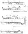
図9は範囲フラグビットを得るために図3の動作を実施する演算を表わす別の流れ図である。
【0021】
図1から図3では本発明の一般的特徴を示す。図1では複数の多ビット要素データ項目を含む複合オペランドを模式的に示す。それぞれの要素について、算術演算でその要素に対する2進出力演算の結果を表わすフラグビットを得られる。図2では図1に示したような技術にしたがって処理装置が実行可能な命令を表わす命令データを有するソフトウェア製品を示す。図3では処理装置を作動させて2進出力演算の結果を表わすフラグビットを取得する際に算術演算を実行させる方法における一般的動作を示す。
【0022】
図1において、複合オペランド10はそれぞれが2ビットを含む要素データ項目12、14、16を含む。要素12は値「10」を有し、要素14は値「01」、また要素16は値「00」を有する。オペランド10において、それぞれの要素はその最上位ビットに隣接してクリアしたビットを有している。
【0023】
定数オペランド20は値「11」の繰り返しよりなり、一回の反復が複合オペランド10内のそれぞれの要素データ項目と位置が揃えてあり、その最上位ビットに隣接してクリアしたビットを有している。値「11」を2ビット値に加算して2ビットの結果を得るのは、(22 −1)=3であるから、2ビット値から値「01」を減算するのと等価である。しかし2ビットの値に「11」を加算すると2ビット値が「01」またはそれ以上の場合に上位側ビットから桁上げビットも生成される。
【0024】
オペランド20をオペランド10に加算すると、2種類の有用な形式の結果が得られる。これはオペランド30として図示してある。ビット32、34、36はそれぞれ要素12、14、16が少なくとも値「01」と同じ大きさかどうかを表わしている。結果データ項目38は要素14が値「01」に等しいことを表わす値「00」を有している。
【0025】
つまりビット32、34、36はそれぞれが要素12、14、16のそれぞれ1つについての2進出力演算の結果を表わすフラグビットである。2進出力演算はそれぞれの要素を閾値「01」と比較する。要素12は「01」より大きいので、ビット32は値「1」を有する。要素14は「01」に等しいので、ビット34も値「1」を有する。しかし要素16は「01」以下なので、ビット36は値「0」となる。
【0026】
結果データ項目38は2ビットを含むため、これからフラグビットを得るにはさらなる動作を行なわなくてはならない。オペランド30を左向きに1ビット桁だけシフトして得られたオペランド40は結果データ項目38と同じ値を有するシフトしたデータ項目42を含むが、これの最下位ビットは結果データ項目38の最上位ビットと位置が揃えてある。
【0027】
オペランド30とオペランド40の論理和でオペランド50が生成される。これのビット22は要素14に対する2進出力演算の結果を表わすフラグビットである。2進出力演算は要素14を値01と等価性の点で比較し、ビット52の値「0」は等価であることを表わしている。同様に、ビット54とビット56は要素12および16が値「01」とは等しくないことを表わす値「1」を有するフラグビットである。
【0028】
図2はソフトウェア製品60を示し、これは図2に図示したのと同様な部材を含むシステム内で使用することが出来る製造物である。ソフトウェア製品60は保存媒体アクセス装置64からアクセス可能なデータ保存媒体62を含む。データ保存媒体62はたとえば1つまたはそれ以上のフロッピーディスクの組などの磁気媒体、1つまたはそれ以上のCD−ROMの組などの光学媒体、半導体メモリ、またはデータを保存するために適切な何らかのほかの媒体であってよい。
【0029】
データ保存媒体62は保存媒体アクセス装置64がたとえばマイクロプロセッサなどで有り得る処理装置66に提供可能なデータを保存する。処理装置66は入力回路70からデータを受信するために接続してある。データは何らかの適切な供給源、たとえばファクシミリ(ファックス)装置や、デジタル複写機のスキャナまたはコンピュータの入出力装置で有り得るようなスキャナ、キーボードとマウスまたはペン型または鉄筆型入力装置などのユーザ入力装置で制御するフォームエディタまたはその他の対話型画像エディタであり得るようなエディタ、またはデータ転送能力を有するローカルエリアネットワークまたはその他のネットワークであり得るようなネットワークなどから取得することが出来る。データは画像に関連したものであり得る。
【0030】
処理装置66はまた出力回路80へデータを提供するためにも接続してある。データはこのあとファクシミリ装置、印刷装置、表示装置、またはネットワークへ提供可能である。印刷装置はデジタル複写機の印刷装置またはコンピュータの入出力装置のことがある。
【0031】
データ保存媒体62に加えて、ソフトウェア製品60は保存媒体62に保存されるデータを含む。保存されたデータは算術演算命令80とフラグビット命令82を表わすデータを含んでいる。処理装置66は命令80を実行して複合オペランド中の複数の要素データ項目のそれぞれについての結果データ項目を得ることが出来る。処理装置66は命令82を実行してそれぞれの要素についての2進出力演算の結果を表わすそれぞれの結果データ項目からフラグビットを得ることが出来る。
【0032】
処理装置66はメモリ84にアクセスすることにより算術演算を実行する要素データ項目を取得することが出来る。それぞれのデータ項目はたとえば画像の画素に関連し得るものである。データ項目はそれぞれ1ビット以上を含むことが出来る。保存媒体62に保存されたデータには、入力回路70から受信したデータ項目をメモリ84内に保存し、演算のためにメモリ84からデータ項目を取り込み、または出力回路72へ提供し、または演算により得られたデータ項目をメモリ84に保存するため処理装置66が実行しうる命令を表わすデータも含むことが可能である。
【0033】
処理装置66は複数の処理桁(processing position) 92を有する処理回路90を含む。処理装置66は、たとえば従来のマイクロプロセッサであってもよい。それぞれの処理桁92では1ビットについての演算を実行することが出来る。処理回路90はアレイを構成させるように処理桁92を対にして接続する桁接続回路94を含む。対の1つの処理桁からの信号は桁接続回路(position connectiong circuitry)94によって別の処理ユニットへ転送することが可能である。
【0034】
演算を実行している複合オペランド中のそれぞれの要素データ項目は処理桁92のそれぞれの部分行列内に存在することが出来る。処理装置66は算術演算命令80を実行してそれぞれの要素の部分行列内にマスクデータ項目を取得できる。処理装置はフラグビット命令82を実行してそれぞれの結果データ項目からフラグビットを取得することが出来る。
【0035】
図3は図2の処理回路90などの処理回路を有する処理装置を作動させる方法における一般的動作を示す。囲み110の動作は複合オペランドを処理回路90に提供するもので、それぞれの要素データ項目が処理桁92のそれぞれの部分行列に提供される。囲み112の動作では処理回路90を作動させて複合オペランドに対し並列に算術演算を実行してそれぞれの部分行列内に結果データ項目を取得している。囲み114の動作ではそれぞれの要素に対して要素についての2進出力演算の結果を表わすフラグビットを得ている。囲み112と114の動作は単一周期で発生し得るもので、これはフラグビットが算術演算により直接生成し得るためである。
【0036】
図1から図3に関して上記で説明した一般的特徴は広範な部材を用いまた各種の演算を用い多様な方法で実施することが出来る。たとえば、上述の一般的特徴の幾つかは従来の処理装置を用いて実施可能であるが、その他の特徴は特別設計の処理装置を用いて実施できるものである。
【0037】
図4から図8では1つ以上のデータ項目に対して並列に演算可能な処理ユニットに応用可能な図3に図示した一般的段階の実施を図示したものである。並列に演算するこのような多数の処理ユニットをこれらの間の桁接続回路を設けまたは設けずに使用することが出来る。
【0038】
図4および図5は算術演算の結果の符号を表わすフラグビットを得るような図3に関連して説明した一般的動作の実施を表わしている。図4において、このようなフラグビットは要素データ項目を閾値と比較する算術演算の結果も表わしている。図5において、このようなフラグビットは2つの要素を比較する算術演算の結果も表わしている。
【0039】
図4において、囲み150の動作ではデータ項目を取得する。それぞれのデータ項目は、たとえば画像の画素に関連することが有り得る。囲み152の動作は囲み150で得られた要素データ項目およびそれぞれの要素データ項目の最上位ビットに隣接するバッファビットを含む複合オペランドを構成する。要素データ項目が直前の画像処理演算から得られたものの場合、囲み150ですでにこの様式を有する複合オペランド内に得られる。囲み152の動作はまた定数値を含み複合オペランド中のそれぞれの要素データ項目に一回づつ発生する定数オペランドも取得している。定数値のそれぞれの所在は複合オペランド中のそれぞれの要素データ項目と位置が揃っておりまた同じ長さを有している。つまり、定数オペランドを複合オペランドから減算する算術演算は複合オペランド中のそれぞれの要素データ項目から閾値Tを減算している。定数オペランドはまた定数値のそれぞれの所在の最上位ビットに隣接してバッファビットも含んでおり、複合オペランド中のそれぞれの要素データ項目に隣接するバッファビットと位置が揃っている。
【0040】
複合オペランドと定数オペランド中のバッファビットはこれについて実行した算術演算の結果が有用となるような値を有するはずである。たとえば、複合オペランド中のすべてのバッファビットは値「1」を有しまた定数オペランド中のすべてのバッファビットは値「0」を有して、結果を無効にすることのある要素間信号を生成することなく複合オペランドから定数オペランドを減算し得るようにしている。
【0041】
囲み154の動作は複合オペランドから定数オペランドを減算しそれぞれの要素データ項目からTが減じられるような算術演算を実行する。したがって囲み154の動作は少なくともTと同じ大きさのそれぞれの要素データ項目について値「1」を有する隣接バッファビットを有する結果データ項目、またTより小さいそれぞれの要素データ項目について借り信号の結果として値「0」を有する隣接バッファビットのある結果データ項目を生成することになる。
【0042】
囲み154の動作は定数を複合オペランドに加算する算術演算に置き換えることが可能である。たとえば、Kビットの要素に(2K −K)を加算すると要素からTを減算して得られた差分と同じ和が得られる。しかしこの場合、両方のオペランドのバッファビットは演算前に値「0」を有するべきである。これは、少なくともTと同じ大きさのそれぞれの要素データ項目について桁上げ信号の結果として値「1」を有する隣接バッファビットを有する結果データ項目、またTより小さいそれぞれの要素データ項目について値「0」を有する隣接バッファビットを有する結果データ項目を生成することになる。
【0043】
囲み156の動作ではフラグビットとして囲み154で生成した結果データ項目に隣接するバッファビットを用いる。この動作は多数の方法で実施可能である。
【0044】
バッファビットだけを含む結果を得るには、縮小などの部分抽出演算を結果データ項目に対して実行する。バッファビットを有するそれぞれの要素データ項目がKビットを含む場合、(K+1):1の縮小を実行するかまたはlog2(K+1)2:1の縮小を実行し、それぞれのビット対の最上位ビットにそれぞれを保存する。これによりバッファビットは要素データ項目が少なくともTと同じ大きさだった画素に関するそれぞれのビットでは1をまた要素データ項目がTより小さかったそれぞれのビットでは0を有するビットマップを構成することになる。
【0045】
多ビット要素データ項目の処理をさらに制御するために使用可能な結果を得るには、バッファビットを用いてマスクを生成することが出来る。
【0046】
図5において、囲み170の動作ではデータ項目の対を得ている。たとえば、2つのデータ項目の両方が画像の同じ画素に関係していることからこれらを対に出来、またはこれらの関連する画素が2枚の異なる画像に由来しているが画像処理の間に一方の画像が他方の上に重ねあわされる際に位置が揃えられていることからこれらを対にすることが出来る。
【0047】
囲み172の動作は第1と第2の複合オペランドを構成しており、これらは囲み170で得られたそれぞれのデータ項目の対の一方を第1の複合オペランドにまた他方を第2のオペランドに分割している。それぞれの複合オペランドは要素データ項目とそれぞれの要素データ項目の最上位ビットに隣接するバッファビットを含む。要素データ項目が直前の画像処理演算から得られた場合には、この様式を有する複合オペランドに囲み170で受信してもよい。対の要素データ項目は相互に位置が揃えてありまた同じ長さで、第2のオペランドを第1のオペランドから減算する算術演算において第2のオペランド内のそれぞれの要素データ項目を第1のオペランド内の対になった要素データ項目から減算する。バッファビットも同様に位置が揃えてあり第1のオペランドには値「1」また第2のオペランドには値「0」を有している。図4に関して述べたように、等価な加算を実行する場合、すべてのバッファビットは値「0」を有しているべきである。
【0048】
囲み174の動作では、第1のオペランドから第2のオペランドを減算する算術演算を実行して、第2のオペランド内のそれぞれの要素データ項目が第1のオペランド内の対になった要素データ項目から減算されるようにする。つまり囲み174の動作では、少なくとも対になった要素データ項目と同じ大きさの第1のオペランド内のそれぞれの要素データ項目について値「1」を有する隣接バッファビットを有する結果データ項目、また対になった要素データ項目より小さい第1のオペランド内のそれぞれの要素データ項目について値「0」を有する隣接バッファビットを有する結果データ項目を借り信号の結果として生成することになる。
【0049】
囲み176の動作では囲み174で生成した結果データ項目に隣接するバッファビットをフラグビットとして用いる。この動作は図4の囲み156に関連して前述したように実施することが出来る。特に、要素データ項目のそれぞれの対の極大を求めるには、第1のマスクをバッファビットから生成し、第2のオペランド内の要素データ項目がこれと対になる要素データ項目と等しいかまたはこれより大きいような桁に「0」を、また第1のオペランド内の要素データ項目のほうが大きい桁では「1」をマスクが含むようにする。第1のマスクと第1のオペランドの論理積から第1のオペランドのマスク版を生成する。第1のマスクを反転させて第2のオペランドとの論理積をとる第2のマスクを生成し、第2のオペランドのマスク板を生成することが出来る。第1と第2のオペランドのマスク版の論理和によってそれぞれの桁で極大の結果を得ることが出来る。逆に、第1のマスクと第2のオペランドの論理積をとり、さらに第2のマスクと第1のオペランドの論理積をとってマスク版を生成し、これの論理和からそれぞれの桁で極小の結果を得ることが出来る。
【0050】
図6および図7は算術演算の結果が0かどうかを示すフラグビットを取得する図3に関連して説明した一般動作の2種類の実施例を示したものである。図6ではこのフラグビットを縮小により取得し、図7ではこのようなフラグビットを並列のさらなる演算で取得している。
【0051】
図6および図7の両方とも図4の囲み154の動作から得られた結果で始めることが出来る。言い換えれば、両方の実施例で、定数オペランドを複合オペランドから減算して結果を得ている。結果は要素データ項目が定数に等しい桁でのみすべて「0」の値を有しそれ以外ではすべて「1」または「1」と「0」の混ざった値を有する。隣接バッファビットは要素データ項目が少なくとも定数と同じ大きさだった場合には「1」それ以外では「0」を有する。結果は図6および図7で図示したようにフラグビットを得るために使用することが出来る。
【0052】
図6において、オペランド180は結果データ項目182、184、186とそれぞれのバッファビット192、194、196を含む。図示したように、データ項目182は定数値をそれより大きい要素データ項目から減算して得られ、データ項目182で「0」に等しくない差分を表わしまたバッファビット192で正の結果を表わす。同様に、データ項目184は定数値を等しい大きさの要素データ項目から減算して得られ、データ項目184で「0」に等しい差分を表わしまたバッファビット194で正の結果を表わす。また、データ項目186は定数値をそれより小さい要素データ項目から減算して得られ、データ項目186で「0」に等しくない差分を表わしまたバッファビット196で負の結果を表わす。
【0053】
バッファビットを反転させるには、XOR(排他的論理和)演算をオペランド180とオペランド200に対して行ない、ビット202、204、206およびバッファビットと位置の揃っているその他のすべてのビットがATA異音を有しまたバッファビットと位置の揃っていないすべてのビットが値オフを有するようにする。つまり排他的論理和演算でオペランド210を生成し、データ項目212、214、216はそれぞれオペランド180のデータ項目182、184、186と同じ値を有するがバッファビット222、224、226はバッファビット192、194、196の逆になるようにする。
【0054】
図6の実施例ではオペランド210に対して部分抽出演算を実行してオペランド230を得ている。部分抽出演算は、オペランド210を1ビット左向きにシフトした後、図1に関連して上述したようにオペランド210とそのシフトした版の論理和をとりさらにそれぞれの対の最上位ビットを選択する2:1縮小で結果を部分抽出してオペランド230を取得することを含むことが出来る。部分抽出はオペランド230を含むテーブルへのインデックスとしてオペランド210を用いて実行することも可能である。
【0055】
ビット232はバッファビット222と要素212の最上位ビットの論理和で得られる。ビット234は要素212の2つの最下位ビットの論理和で得られる。ビット236はバッファビット224と要素214の最上位ビットの論理和で得られる。ビット237は要素214の2つの最下位ビットの論理和で得られる。ビット238はバッファビット226と要素216の最上位ビットの論理和で得られる。ビット239は要素216の2つの最下位ビットの論理和で得られる。
【0056】
次に、図6の実施ではオペランド230に対して別の部分抽出演算を実行してオペランド240を得ている。ビット242はビット232と234の論理和、ビット244はビット236と237の論理和、ビット246はビット238と239の論理和でそれぞれ得られる。ビット242、244、246は結果データ項目184が0結果を表わしまたデータ項目182と186が「0」に等しくない結果を表わしていることを示すフラグビットである。
【0057】
図7のオペランド250は図6のオペランド210と同一のもので、データ項目252、254、256とバッファビット262、264、266を有する。オペランド250はバッファビットをクリアするためのオフの値272とそれ以外でオンの値274を有するマスク270と第1に論理和をとる。つまりオペランド280はバッファビット282、284、286をクリアしたことになる。
【0058】
次にオペランド280をクリアしたバッファビット292とすべての桁で「1」を含む定数値294を有する定数オペランド290に加算する。オペランド300は結果データ項目と、図6のビット232、234、236とそれぞれ同じ値を有するフラグビットのバッファビット302、304、306を含む。これらのフラグビットを図4の囲み156との関連で上述したように使用することが出来る。
【0059】
フラグビットを得るためにバッファビットからの情報は必要ではなくまたバッファビットをフラグビットとして使用しないので、図6の実施はバッファビットのない結果データ項目にも応用することが可能である。図7の実施はバッファ人からの情報を必要としないが、バッファビットをフラグビットとして使用しているので、結果データ項目がバッファビットを有していない場合、バッファビットを挿入する必要がある。
【0060】
それぞれの結果データ値とバッファビットの和にKビット含む場合、バッファビットフラグに対して一連の(K−1)シフトと図1に関連して前述の形式の論理和演算を行なうことにより得ることが可能となる。比較すると、図6の実施はlog2Kシフトと論理和演算およびlog2K部分抽出演算で実施でき、これは高速な部分抽出演算が利用可能であれば大きなKの値に対して有利である。図7の実施はオペランド270と290が利用可能であれば図示したように2回の演算で実行できる。したがって「0」フラグビットを得る演算をどのように実施するかの選択は処理装置の能力と効率を含んだ勘案に基づいて行なうことが出来る。
【0061】
図8および図9では、要素データ項目のそれぞれが範囲内であるかを表わす範囲フラグビットをそれぞれに取得する2種類の実施を図示する。
【0062】
図8において、囲み320の動作では、図4に関連して前述の複合オペランドに対する2種類の演算を実行してそれぞれの要素データ項目について第1と第2の符号フラグビットを得ている。1つの演算では定数値(T1 +1)をまた他方では定数値T2 を使用する。ここでT2 >T1 である。その結果、要素の第1のフラグビットは要素が(T1 +1)と同じ大きさかを表わし、第2のフラグビットは要素がT2 と同じ大きさかを表わしている。複合オペランド中の要素の第1のフラグビットは第1のオペランド内にまた第2のフラグビットは第2のオペランド内にある。
【0063】
囲み322の動作は第2のオペランドを反転させる。反転した第2のフラグビットが値「1」を有する要素はT2 より小さく、一方第1のフラグビットが値「1」を有する要素はT1 より大きい。
【0064】
囲み324の動作では第1のオペランドと反転した第2のオペランドの論理積をとって、それぞれ要素がT1 とT2 の範囲内にあるかを表わす範囲フラグビットを生成する。要素の範囲フラグビットは要素が範囲内にある場合は値「1」を有しそうではない場合は値「0」を有する。
【0065】
定数値(T1 +1)とT2 を図8の実施において用い、T1 とT2 で区切られた開放範囲、(T1 +1)と(T2 −1)で区切られた閉鎖範囲、または一端では開放し他端では閉じている範囲についての範囲フラグビットを取得することが出来る。
【0066】
図9において、囲み340の動作では図4に関連して前述したように複合オペランドに対する演算を実行してそれぞれの要素データ項目に符号フラグビットを有する第1のオペランドを得ている。演算には定数値T1 を用い、これをそれぞれの要素データ項目から減算する。その結果、第1のオペランド内の要素のフラグビットは要素がT1 と同じ大きさかを表わす。さらに、第1のオペランド内のそれぞれの要素の結果データ項目はT1 で下向きにシフトした値を有し、T1 より小さかった要素は2K と(2K −T1 )の間の値にシフトされる。
【0067】
囲み342の動作では第1のオペランドに対して演算を行ない全てのバッファビットを値「1」に設定している。これは減算演算の準備である。
【0068】
囲み344の動作では、図4に関連して述べたように別の演算を実行してそれぞれの要素データ項目について符号フラグビットを有する第2のオペランドを取得する。この演算は、囲み342で変更したように、定数値(T2 −T1 )を第1のオペランド内のそれぞれの要素の結果データ項目から減算するものである。その結果、第2のオペランド内の要素のフラグビットはその要素がT1 とT2 の間の範囲にあるかを示す。ここでT2 >T1 である。要素が範囲内の場合、第2のオペランド中のこれの符号フラグビットは借り信号のために値「0」を有する。要素が範囲以上または以下の場合、第2のオペランド中のこれの符号フラグビットは値「1」を有する。
【0069】
図8におけるように、図9の実施でも開放または閉鎖範囲を使用することが可能である。
【0070】
上述の一般的実施の特徴は広範なデータ処理用途に使用可能である。しかしある種の画像処理においてはそれぞれの要素データ項目について順次実行するよりも迅速に実行しうることで特に有用であると推測される。特に、上述の特徴をセラ(Serra, J. )の「画像分析と数学的変換(Image Analysis and Mathematical Morphology)」、アカデミックプレス刊、1982年、およびセラ(Serra, J. )の「画像分析と数学的変換第2巻:理論的な進歩(Image Analysis and Mathematical Morphology, Volume 2: Theoretical Advances )」、アカデミックプレス刊、1988年、に解説されているのと同様の技術を実施するために使用することが出来る。このような技術はたとえば雑音の除去またはその他の情報を含まない特徴の除去、歪曲補正、データ符号化、自動フォーム作成または制御シート作成のための部分の抽出、印刷装置特有の補正などの文書サービスを提供するために使用することが出来る。このような文書サービスは、ファクシミリ装置および複写装置を含むデジタル複写装置において、印刷装置またはその他の画像出力装置用の画像を定義するデータを生成する装置において、スキャナまたはその他の画像入力装置から受信した画像を定義するデータについて演算するまた画像処理を行なうその他の装置において、使用することが出来る。
【0071】
上述の特徴は広範な画像処理演算の間にグレースケールまたはカラー画素値に対してフラグビットを取得するために使用できる。
【0072】
上述の一般的実施の特徴はまた、各種のその他の用途において、たとえば特定の特徴の組み合わせを含む画像について画像データベースの検索や、封筒の住所の走査、高速スキャナからのフォームの解釈、人工視覚、および処理に特有の印刷画像の補正および確認などにおいても有用であろう。
【0073】
本発明は各種のその他の画像処理演算、たとえば画素の計数、グレースケールの形態変更、グレースケールの回転、エラー分散画像の生成および歪曲検出などを実行するために応用することも可能である。
【0074】
本発明は画像に関連しないデータに使用することも可能である。本発明はたとえば有限微分解析または物理現象のシミュレーションを実行するために使用することが出来る。
【0075】
本発明は幾つかの実施に関連して説明した。本発明は2つまたはそれ以上の実施を組合せて用いることで、または2つまたはそれ以上の実施から得られたフラグビットに対して論理演算を行なうことによって、組み合わせフラグビットを取得するために実施することも可能である。
【0076】
本発明は複合オペランド中の要素データ項目が単一のバッファビットで分離されているような実施に関連して説明した。本発明は要素間に複数のバッファビットを有するように実施することも出来る。
【0077】
本発明は加算と減算を用いてフラグビットを取得する実施に関連して説明した。その他の算術演算を用いてフラグビットを取得することも可能である。
【0078】
本発明は画像に関連するデータについて演算する実施に関連して説明したが、画像に関連しないデータに対して演算を行なうために実施してもよい。
【0079】
本発明は従来のマイクロプロセッサを用いた実施に関連して説明したが、本発明は縮小命令セット計算機(RISC)チップを用いてまたはメインフレーム・コンピュータ、ミニコンピュータ、スーパーコンピュータ、または何らかのその他の計算機の処理装置を含む何らかのその他の処理装置を用いて実施してもよい。
【0080】
本発明は処理装置とメモリを含むシステム内で使用するためのメモリからのデータに対して演算を実行するために処理装置が実行できる命令を表わすデータを含むようなソフトウェア製品に関連して説明した。システムのメモリは当然のことながらシステム内で使用する際にソフトウェア製品を含み、命令ならびにデータは一般に処理装置からアクセス可能な何らかのメモリ装置内に任意に保存することが出来る。たとえば、本発明はソフトウェア製品内にではなくメモリ内に保存された命令を表わすデータを用いて容易に実施することが可能である。
【0081】
本発明は単純な構造の複合オペランドに関連して説明した。上述の実施例において、全ての要素データ項目はおなじ長さであり複合オペランド内部の要素は相互に関連していなくとも良い。本発明は処理装置の幅の制約内で、さらなる構造を有する複合オペランドで実施することも可能である。たとえば、複合オペランドは、他のオペランドが同じ位置にある同じ幅の要素と位置が揃っているならば、異なる幅の要素データ項目を含んでいてもよい。また、要素データ項目は2つまたはそれ以上のグループに構成され、それぞれのグループの要素が関連していてもよい。それぞれのグループの要素が同じ画素に関連している場合、それぞれの要素はそれぞれの閾値減少のための値を保持することが可能である。より一般的には、それぞれのグループ内の要素が物理的シミュレーション空間内の同じ位置に関連している場合、1つの要素がその位置での値を保持しまた別の位置がその位置での導関数を保持することが可能である。
【図面の簡単な説明】
【図1】 2進出力演算の結果を表わすフラグビットを得るためにどのように並列に算術演算を実行することが出来るかの実施例を示す概略流れ図である。
【図2】 並列に算術演算を実行することによりフラグビットを得るためソフトウェア製品からの命令を処理装置が実行し得るようなシステムの部材を表わす概略ブロック図である。
【図3】 並列に算術演算を実行することによりフラグビットを得る上での一般的動作を表わす流れ図である。
【図4】 複合データ項目と定数の比較を行なう符号フラグビットを得るために図3での動作を実施する演算を表わす流れ図である。
【図5】 2つの要素データ項目の比較を行なう符号フラグビットを得るために図3での動作を実施する演算を表わす流れ図である。
【図6】 部分抽出演算で0フラグビットを得るために図3の動作を実施する演算を表わす概略流れ図である。
【図7】 算術および論理演算で0フラグビットを得るために図3の動作を実施する演算を表わす概略流れ図である。
【図8】 範囲フラグビットを得るために図3の動作を実施する演算を表わす流れ図である。
【図9】 範囲フラグビットを得るために図3の動作を実施する演算を表わす別の流れ図である。
【符号の説明】
10 複合オペランド、12,14,16 要素データ項目、20 定数オペランド、30 オペランド、32,34,36 要素、38 結果データ項目、40 オペランド、42 シフトしたデータ項目、50 オペランド、60 ソフトウェア、62 データ保存媒体、66 処理装置、80 算術演算命令、82フラグビット命令、84 メモリ、90 処理回路、92 処理桁、180オペランド、182,184,186 要素データ項目、190 オペランド、192,194,196 バッファビット、200 オペランド、202,204,206 ビット、210 オペランド、212,214,216 データ項目、220 オペランド、222,224,226 バッファビット、230オペランド、232,234,236,237,238,239 ビット、240 オペランド、242,244,246 ビット、250 オペランド、252,254,256 データ項目、262,264,266 バッファビット、270 マスク、280 オペランド、282,284,286 バッファビット、290 定数オペランド、292 バッファビット、294 定数、300オペランド、302,304,306 バッファビット[0001]
The present invention relates to a technique for performing an operation on a plurality of data items.
[0002]
Many prior arts perform operations on multiple data items. Some examples are found in the field of image processing where each data item can be associated with a pixel in the image.
[0003]
Mahoney European Patent No. 460,970 discloses a hierarchical data analysis technique applicable to pixel values. FIG. 7 illustrates a connection machine system that performs image processing by simulating a binary image jungle (BIJ). A front-end processor (FEP) makes a call to cause a processing unit in the connection machine to perform arithmetic and logical operations. FIG. 8 shows a part of an array of processing units in the connection machine, where one processing unit stores one pixel value.
[0004]
Bloomberg et al., European Patent No. 431,961, discloses a technique for reducing and enlarging an image. Disclosed is a method for reducing a binarized image by performing a logical operation between bits on the second page from the 18th line to the third page, the 18th line, and from the fifth page, the 50th line to the sixth page, the 31st line. ing. The third page, lines 36-58, discloses a technique for operations on a very wide range of pixel words, including logically integrating the pixel word and its own variation after shifting the pixel word. doing.
[0005]
The present invention addresses problems in processing multi-bit data items such as gray scale and color pixel values.
[0006]
An operation on a multi-bit data item is often a conditional expression. For example, a data item may be manipulated in one way if it is not likely to be manipulated in one way if it exceeds a threshold. Or it may be operated only when the data item is equal to a predetermined value or within a certain range. That is, it is often necessary to execute an operation that generates a binary value for determining whether a data item meets a condition, as referred to herein as a binary output operation.
[0007]
Binary output operations are also useful for other purposes. For example, data items that meet the conditions can be counted by integrating the binary logical results for the array of data items.
[0008]
The prior art can be used to perform binary output operations on data items. For example, the microprocessor can perform an operation that compares two data items to determine if they are equivalent or whether one exceeds the other.
[0009]
However, in the prior art, a single processor can only operate on one multi-bit data item at a time. Conventionally, a processor cannot perform binary output operations in parallel on several multi-bit data items that are each narrower than the processor.
[0010]
The present invention is based on the discovery of a technique for performing binary output operations in parallel on composite operands containing multiple multi-bit element data items. The element data item can be, for example, a gray scale or a color pixel value. In this technique, data representing a binary output is generated for each element using an arithmetic operation. Arithmetic operations can be added or subtracted, for example.
[0011]
The present technique can be implemented by operating a processor to perform arithmetic operations on composite operands containing multiple multi-bit element data items. Arithmetic operations generate result data items for each element. A flag bit is also obtained for each element. Each flag bit represents a binary output for that element.
[0012]
FIG. 1 is a schematic flow diagram illustrating an embodiment of how arithmetic operations can be performed in parallel to obtain a flag bit representing the result of a binary output operation.
[0013]
FIG. 2 is a schematic block diagram illustrating the components of a system in which a processor may execute instructions from a software product to obtain flag bits by performing arithmetic operations in parallel.
[0014]
FIG. 3 is a flow diagram illustrating the general operation for obtaining flag bits by performing arithmetic operations in parallel.
[0015]
FIG. 4 is a flow chart representing operations that perform the operations in FIG. 3 to obtain a sign flag bit that compares a composite data item with a constant.
[0016]
FIG. 5 is a flow chart representing operations that perform the operations in FIG. 3 to obtain a code flag bit that compares two element data items.
[0017]
FIG. 6 is a schematic flowchart showing an operation for performing the operation of FIG. 3 in order to obtain the 0 flag bit in the partial extraction operation.
[0018]
FIG. 7 is a schematic flow diagram illustrating operations that perform the operations of FIG. 3 to obtain 0 flag bits in arithmetic and logical operations.
[0019]
FIG. 8 is a flow chart representing operations that perform the operations of FIG. 3 to obtain range flag bits.
[0020]
FIG. 9 is another flow diagram representing operations that perform the operations of FIG. 3 to obtain range flag bits.
[0021]
1 to 3 show the general features of the present invention. FIG. 1 schematically shows a composite operand including a plurality of multi-bit element data items. For each element, a flag bit representing the result of the binary output operation for that element can be obtained by an arithmetic operation. FIG. 2 shows a software product having instruction data representing instructions that can be executed by the processing device according to the technique shown in FIG. FIG. 3 shows a general operation in a method for executing an arithmetic operation when the processor is operated to acquire a flag bit representing the result of the binary output operation.
[0022]
In FIG. 1,
[0023]
The
[0024]
Adding
[0025]
That is,
[0026]
Since the
[0027]
[0028]
FIG. 2 illustrates a
[0029]
[0030]
The
[0031]
In addition to the
[0032]
The
[0033]
The
[0034]
Each element data item in the composite operand performing the operation can be present in each submatrix of
[0035]
FIG. 3 illustrates the general operation in a method of operating a processing apparatus having a processing circuit, such as
[0036]
The general features described above with respect to FIGS. 1-3 can be implemented in a variety of ways using a wide variety of components and various operations. For example, some of the general features described above can be implemented using conventional processing equipment, while other features can be implemented using specially designed processing equipment.
[0037]
FIGS. 4-8 illustrate the implementation of the general steps illustrated in FIG. 3 applicable to a processing unit that can operate in parallel on one or more data items. A large number of such processing units operating in parallel can be used with or without a girder connection circuit between them.
[0038]
4 and 5 represent the implementation of the general operation described in connection with FIG. 3 to obtain a flag bit representing the sign of the result of the arithmetic operation. In FIG. 4, such flag bits also represent the result of an arithmetic operation that compares the element data item with a threshold. In FIG. 5, such flag bits also represent the result of an arithmetic operation that compares two elements.
[0039]
In FIG. 4, the data item is acquired in the operation of the
[0040]
The buffer bits in the compound and constant operands should have values that will be useful for the results of arithmetic operations performed on them. For example, all buffer bits in a composite operand have the value “1” and all buffer bits in a constant operand have the value “0” to generate an inter-element signal that can invalidate the result. The constant operand can be subtracted from the composite operand without doing so.
[0041]
The act in box 154 performs an arithmetic operation that subtracts the constant operand from the composite operand and subtracts T from each element data item. Thus, the act in box 154 is a result data item having an adjacent buffer bit having a value “1” for each element data item that is at least as large as T, and a value as a result of the borrow signal for each element data item less than T. A result data item with adjacent buffer bits having "0" will be generated.
[0042]
The act in box 154 can be replaced with an arithmetic operation that adds a constant to the composite operand. For example, for a K-bit element (2 K When -K) is added, the same sum as the difference obtained by subtracting T from the element is obtained. In this case, however, the buffer bits of both operands should have the value “0” before the operation. This is a result data item having an adjacent buffer bit having a value “1” as a result of the carry signal for at least each element data item of the same size as T, and a value “0” for each element data item less than T. Result data item having adjacent buffer bits with "".
[0043]
The operation in
[0044]
To obtain a result that includes only buffer bits, a partial extraction operation such as reduction is performed on the result data item. If each element data item with buffer bits contains K bits, perform (K + 1): 1 reduction or log 2 Perform a (K + 1) 2: 1 reduction and store each in the most significant bit of each bit pair. Thus, the buffer bits constitute a bitmap having 1 for each bit associated with a pixel whose element data item was at least as large as T and 0 for each bit whose element data item was less than T.
[0045]
To obtain results that can be used to further control the processing of multi-bit element data items, a mask can be generated using buffer bits.
[0046]
In FIG. 5, in the operation of the
[0047]
The act in
[0048]
The act in
[0049]
In the operation of
[0050]
6 and 7 show two examples of the general operation described with reference to FIG. 3 for obtaining a flag bit indicating whether the result of the arithmetic operation is 0 or not. In FIG. 6, this flag bit is obtained by reduction, and in FIG. 7, such a flag bit is obtained by further operations in parallel.
[0051]
Both FIG. 6 and FIG. 7 can begin with the results obtained from the operation of box 154 of FIG. In other words, in both embodiments, the constant operand is subtracted from the composite operand to obtain the result. The result is that all element data items have a value of “0” only in digits equal to a constant, and all other values have a value of “1” or a mixture of “1” and “0”. The adjacent buffer bit has “1” if the element data item is at least as large as the constant, and “0” otherwise. The result can be used to obtain flag bits as illustrated in FIGS.
[0052]
In FIG. 6,
[0053]
To invert the buffer bit, an XOR (exclusive OR) operation is performed on
[0054]
In the embodiment of FIG. 6, a partial extraction operation is performed on the
[0055]
[0056]
Next, in the implementation of FIG. 6, another partial extraction operation is performed on the
[0057]
The
[0058]
Next, the
[0059]
Since no information from the buffer bits is needed to obtain the flag bits, and the buffer bits are not used as flag bits, the implementation of FIG. 6 can be applied to result data items without buffer bits. The implementation of FIG. 7 does not require information from the buffer person, but uses buffer bits as flag bits, so if the resulting data item does not have buffer bits, it is necessary to insert buffer bits.
[0060]
When K bits are included in the sum of each result data value and the buffer bit, the buffer bit flag is obtained by performing a series of (K-1) shifts and the above-described logical OR operation in relation to FIG. Is possible. In comparison, the implementation of FIG. 2 K shift and logical sum operation and log 2 This can be done with a K partial extraction operation, which is advantageous for large K values if a fast partial extraction operation is available. The implementation of FIG. 7 can be performed in two operations as shown if
[0061]
FIGS. 8 and 9 illustrate two types of implementations that each acquire a range flag bit that indicates whether each element data item is within range.
[0062]
In FIG. 8, in the operation of the box 320, two types of operations are performed on the composite operand described above with reference to FIG. 4 to obtain the first and second sign flag bits for each element data item. In one operation, a constant value (T 1 +1) and on the other hand a constant value T 2 Is used. Where T 2 > T 1 It is. As a result, the first flag bit of the element has the element (T 1 +1) and the second flag bit has an element T 2 Is the same size. The first flag bit of the element in the composite operand is in the first operand and the second flag bit is in the second operand.
[0063]
The act in
[0064]
In the operation of
[0065]
Constant value (T 1 +1) and T 2 Is used in the implementation of FIG. 1 And T 2 Open range separated by (T 1 +1) and (T 2 It is possible to obtain a range flag bit for a closed range divided by -1), or a range that is open at one end and closed at the other end.
[0066]
9, the operation of
[0067]
In the operation of
[0068]
The act in
[0069]
As in FIG. 8, the implementation of FIG. 9 can also use open or closed ranges.
[0070]
The general implementation features described above can be used in a wide variety of data processing applications. However, it is presumed that it is particularly useful in certain types of image processing because it can be executed more quickly than sequential execution for each element data item. In particular, the features described above are described by Serra, J. “Image Analysis and Mathematical Morphology”, Academic Press, 1982, and Serra, J. Used to implement techniques similar to those described in Mathematical Transformation Vol. 2: Image Analysis and Mathematical Morphology, Volume 2: Theoretical Advances, Academic Press, 1988. I can do it. Such techniques include document services such as noise removal or other non-informational feature removal, distortion correction, data encoding, extraction of parts for automatic form creation or control sheet creation, printing device specific correction, etc. Can be used to provide Such document services are received from a scanner or other image input device in a digital copying device including a facsimile device and a copying device, in a device that generates data defining an image for a printing device or other image output device. It can be used in other devices that operate on data defining an image and perform image processing.
[0071]
The features described above can be used to obtain flag bits for grayscale or color pixel values during a wide range of image processing operations.
[0072]
The general implementation features described above may also be used in various other applications, such as searching an image database for images containing a combination of specific features, scanning envelope addresses, interpreting forms from high-speed scanners, artificial vision, In addition, it may be useful for correction and confirmation of a print image specific to processing.
[0073]
The present invention can also be applied to perform various other image processing operations, such as pixel counting, grayscale shape change, grayscale rotation, error variance image generation and distortion detection.
[0074]
The present invention can also be used for data not related to images. The present invention can be used, for example, to perform finite differential analysis or simulation of physical phenomena.
[0075]
The invention has been described with reference to several implementations. The present invention is implemented to obtain a combined flag bit by using a combination of two or more implementations or by performing a logical operation on the flag bits obtained from the two or more implementations. It is also possible to do.
[0076]
The present invention has been described in connection with implementations where element data items in a composite operand are separated by a single buffer bit. The present invention can also be implemented with multiple buffer bits between elements.
[0077]
The invention has been described in relation to implementations that obtain flag bits using addition and subtraction. It is also possible to obtain flag bits using other arithmetic operations.
[0078]
Although the present invention has been described in relation to implementations that operate on data related to images, it may also be implemented to perform operations on data that is not related to images.
[0079]
Although the present invention has been described in connection with implementations using conventional microprocessors, the present invention uses reduced instruction set calculator (RISC) chips or mainframe computers, minicomputers, supercomputers, or some other computer. Any other processing apparatus including the above processing apparatus may be used.
[0080]
The present invention has been described in connection with a software product that includes data representing instructions that can be executed by a processing unit to perform operations on data from memory for use in a system including the processing unit and memory. . The system's memory, of course, includes software products when used in the system, and instructions and data can optionally be stored in any memory device that is generally accessible from the processing unit. For example, the present invention can be easily implemented using data representing instructions stored in memory rather than in a software product.
[0081]
The present invention has been described with reference to a complex operand of simple structure. In the above embodiment, all element data items have the same length, and the elements inside the composite operand need not be related to each other. The present invention can also be implemented with compound operands having additional structure within the constraints of the processor width. For example, a composite operand may contain element data items of different widths if they are aligned with elements of the same width where other operands are at the same position. In addition, the element data items may be configured in two or more groups, and the elements of each group may be related. If each group of elements is associated with the same pixel, each element can hold a value for its respective threshold reduction. More generally, if an element in each group is associated with the same position in the physical simulation space, one element holds a value at that position and another position derives at that position. It is possible to hold functions.
[Brief description of the drawings]
FIG. 1 is a schematic flow diagram illustrating an embodiment of how arithmetic operations can be performed in parallel to obtain a flag bit representing the result of a binary output operation.
FIG. 2 is a schematic block diagram illustrating the components of a system in which a processing unit can execute instructions from a software product to obtain flag bits by performing arithmetic operations in parallel.
FIG. 3 is a flow chart representing a general operation for obtaining flag bits by performing arithmetic operations in parallel.
FIG. 4 is a flow chart representing operations that perform the operations in FIG. 3 to obtain a sign flag bit that compares a composite data item with a constant.
FIG. 5 is a flow chart representing operations that perform the operations in FIG. 3 to obtain a code flag bit that compares two element data items.
FIG. 6 is a schematic flowchart showing an operation for performing the operation of FIG. 3 in order to obtain a 0 flag bit by a partial extraction operation.
FIG. 7 is a schematic flow diagram representing operations that perform the operations of FIG. 3 to obtain 0 flag bits in arithmetic and logical operations.
FIG. 8 is a flow diagram representing operations that perform the operations of FIG. 3 to obtain range flag bits.
FIG. 9 is another flow diagram representing operations that perform the operations of FIG. 3 to obtain range flag bits.
[Explanation of symbols]
10 complex operands, 12, 14, 16 element data items, 20 constant operands, 30 operands, 32, 34, 36 elements, 38 result data items, 40 operands, 42 shifted data items, 50 operands, 60 software, 62 data storage Medium, 66 processing unit, 80 arithmetic operation instruction, 82 flag bit instruction, 84 memory, 90 processing circuit, 92 processing digit, 180 operand, 182, 184, 186 element data item, 190 operand, 192, 194, 196 buffer bit, 200 operands, 202, 204, 206 bits, 210 operands, 212, 214, 216 data items, 220 operands, 222, 224, 226 buffer bits, 230 operands, 232, 234, 236, 237, 238, 239 Bits, 240 operands, 242, 244, 246 bits, 250 operands, 252, 254, 256 data items, 262, 264, 266 buffer bits, 270 mask, 280 operands, 282, 284, 286 buffer bits, 290 constant operands, 292 Buffer bits, 294 constants, 300 operands, 302, 304, 306 buffer bits
Claims (1)
前記処理装置は算術演算を実行する処理回路を有し、前記処理回路は4桁以上の処理桁を有し、それぞれの処理桁は1ビットに対する演算を実行するためのものであり、前記処理回路は処理桁のアレイを形成するために処理桁を接続する桁接続回路を含み、
前記方法が、
前記処理回路に第1及び第2の複合オペランドを提供する段階であって、前記第1及び第2の複合オペランドはそれぞれが1ビット以上を含む2つ以上の要素データ項目を含み、それぞれの要素データ項目は前記アレイにおける処理桁のそれぞれのサブアレイに提供されるものであり、前記第1及び第2の複合オペランドの要素データ項目は一列に揃えられてフラグビット桁によって分割されるようにサブアレイ内に位置し、これによってそれぞれのサブアレイが隣接するフラグビット桁を有するようにする段階と、
前記第1及び第2の複合オペランドに対して算術演算を並列して実行するために前記処理装置を作動させる段階であって、前記算術演算は、それぞれのサブアレイにおいてそれぞれが1ビット以上を含む複数の要素データ項目を含むそれぞれの結果データ項目を取得し、かつ、サブアレイに隣接するそれぞれのフラグビット桁において前記要素データ項目についての2進出力演算の結果を表わすフラグビットを取得する段階とを含む処理装置を作動させる方法。 A method of operating a processing apparatus,
The processing device has a processing circuit for performing arithmetic operations, the processing circuit has processing digits of four digits or more, and each processing digit is for performing an operation on one bit, and the processing circuit Includes digit connection circuitry for connecting the processing digits to form an array of processing digits;
The method comprises
Providing first and second compound operands to the processing circuit, wherein the first and second compound operands include two or more element data items each including one or more bits, each element Data items are provided in respective sub-arrays of processing digits in the array, and the element data items of the first and second composite operands are aligned in a row and divided by flag bit digits. , So that each sub-array has adjacent flag bit digits,
Activating the processing unit to perform arithmetic operations on the first and second composite operands in parallel, the arithmetic operations comprising a plurality of arithmetic operations each including one or more bits in each sub-array; Obtaining each result data item including the element data item and obtaining a flag bit representing a result of the binary output operation for the element data item in each flag bit digit adjacent to the sub-array. A method of operating a processing device .
Applications Claiming Priority (2)
| Application Number | Priority Date | Filing Date | Title |
|---|---|---|---|
| US07/993,213 US5375080A (en) | 1992-12-18 | 1992-12-18 | Performing arithmetic on composite operands to obtain a binary outcome for each multi-bit component |
| US993213 | 2001-11-16 |
Publications (2)
| Publication Number | Publication Date |
|---|---|
| JPH06222906A JPH06222906A (en) | 1994-08-12 |
| JP3637923B2 true JP3637923B2 (en) | 2005-04-13 |
Family
ID=25539249
Family Applications (1)
| Application Number | Title | Priority Date | Filing Date |
|---|---|---|---|
| JP31778293A Expired - Lifetime JP3637923B2 (en) | 1992-12-18 | 1993-12-17 | Method for operating a processing device |
Country Status (4)
| Country | Link |
|---|---|
| US (1) | US5375080A (en) |
| EP (1) | EP0602887B1 (en) |
| JP (1) | JP3637923B2 (en) |
| DE (1) | DE69328071T2 (en) |
Families Citing this family (22)
| Publication number | Priority date | Publication date | Assignee | Title |
|---|---|---|---|---|
| US5651121A (en) * | 1992-12-18 | 1997-07-22 | Xerox Corporation | Using mask operand obtained from composite operand to perform logic operation in parallel with composite operand |
| US5655131A (en) * | 1992-12-18 | 1997-08-05 | Xerox Corporation | SIMD architecture for connection to host processor's bus |
| US5519649A (en) * | 1993-06-04 | 1996-05-21 | Nippon Steel Corporation | Micro-processor having rapid condition comparison function |
| JP3711147B2 (en) * | 1995-08-31 | 2005-10-26 | インテル・コーポレーション | A set of instructions that process packed data |
| US6036350A (en) * | 1995-12-20 | 2000-03-14 | Intel Corporation | Method of sorting signed numbers and solving absolute differences using packed instructions |
| US5907842A (en) * | 1995-12-20 | 1999-05-25 | Intel Corporation | Method of sorting numbers to obtain maxima/minima values with ordering |
| US6009451A (en) * | 1996-11-22 | 1999-12-28 | Lucent Technologies Inc. | Method for generating barrel shifter result flags directly from input data |
| GB2362731B (en) | 2000-05-23 | 2004-10-06 | Advanced Risc Mach Ltd | Parallel processing of multiple data values within a data word |
| US7007172B2 (en) | 2001-06-01 | 2006-02-28 | Microchip Technology Incorporated | Modified Harvard architecture processor having data memory space mapped to program memory space with erroneous execution protection |
| US20020184566A1 (en) | 2001-06-01 | 2002-12-05 | Michael Catherwood | Register pointer trap |
| US6952711B2 (en) | 2001-06-01 | 2005-10-04 | Microchip Technology Incorporated | Maximally negative signed fractional number multiplication |
| US7003543B2 (en) * | 2001-06-01 | 2006-02-21 | Microchip Technology Incorporated | Sticky z bit |
| US7020788B2 (en) | 2001-06-01 | 2006-03-28 | Microchip Technology Incorporated | Reduced power option |
| US7467178B2 (en) | 2001-06-01 | 2008-12-16 | Microchip Technology Incorporated | Dual mode arithmetic saturation processing |
| US6976158B2 (en) | 2001-06-01 | 2005-12-13 | Microchip Technology Incorporated | Repeat instruction with interrupt |
| US6934728B2 (en) | 2001-06-01 | 2005-08-23 | Microchip Technology Incorporated | Euclidean distance instructions |
| US6985986B2 (en) | 2001-06-01 | 2006-01-10 | Microchip Technology Incorporated | Variable cycle interrupt disabling |
| US6975679B2 (en) | 2001-06-01 | 2005-12-13 | Microchip Technology Incorporated | Configuration fuses for setting PWM options |
| US6937084B2 (en) | 2001-06-01 | 2005-08-30 | Microchip Technology Incorporated | Processor with dual-deadtime pulse width modulation generator |
| US8037120B2 (en) * | 2006-12-05 | 2011-10-11 | Analog Devices, Inc. | System and method for an efficient comparison operation of multi-bit vectors in a digital logic circuit |
| US8363984B1 (en) | 2010-07-13 | 2013-01-29 | Google Inc. | Method and system for automatically cropping images |
| US9070182B1 (en) | 2010-07-13 | 2015-06-30 | Google Inc. | Method and system for automatically cropping images |
Family Cites Families (11)
| Publication number | Priority date | Publication date | Assignee | Title |
|---|---|---|---|---|
| US4161784A (en) * | 1978-01-05 | 1979-07-17 | Honeywell Information Systems, Inc. | Microprogrammable floating point arithmetic unit capable of performing arithmetic operations on long and short operands |
| JPS5765194A (en) * | 1980-10-09 | 1982-04-20 | Daicel Chem Ind Ltd | Microbial preparation of unsaturated dicarboxylic acid |
| US4742552A (en) * | 1983-09-27 | 1988-05-03 | The Boeing Company | Vector image processing system |
| US4789957A (en) * | 1986-03-28 | 1988-12-06 | Texas Instruments Incorporated | Status output for a bit slice ALU |
| US4811266A (en) * | 1986-11-05 | 1989-03-07 | Honeywell Bull Inc. | Multifunction arithmetic indicator |
| US5129092A (en) * | 1987-06-01 | 1992-07-07 | Applied Intelligent Systems,Inc. | Linear chain of parallel processors and method of using same |
| JP3076046B2 (en) * | 1989-01-31 | 2000-08-14 | 日本電気株式会社 | Exception detection circuit |
| JP2523222B2 (en) * | 1989-12-08 | 1996-08-07 | ゼロックス コーポレーション | Image reduction / enlargement method and apparatus |
| US5280547A (en) * | 1990-06-08 | 1994-01-18 | Xerox Corporation | Dense aggregative hierarhical techniques for data analysis |
| JPH0454679A (en) * | 1990-06-25 | 1992-02-21 | Nec Corp | Arithmetic unit |
| JP2601960B2 (en) * | 1990-11-15 | 1997-04-23 | インターナショナル・ビジネス・マシーンズ・コーポレイション | Data processing method and apparatus |
-
1992
- 1992-12-18 US US07/993,213 patent/US5375080A/en not_active Expired - Lifetime
-
1993
- 1993-12-08 DE DE69328071T patent/DE69328071T2/en not_active Expired - Lifetime
- 1993-12-08 EP EP93309862A patent/EP0602887B1/en not_active Expired - Lifetime
- 1993-12-17 JP JP31778293A patent/JP3637923B2/en not_active Expired - Lifetime
Also Published As
| Publication number | Publication date |
|---|---|
| EP0602887A1 (en) | 1994-06-22 |
| EP0602887B1 (en) | 2000-03-15 |
| DE69328071T2 (en) | 2000-07-13 |
| US5375080A (en) | 1994-12-20 |
| JPH06222906A (en) | 1994-08-12 |
| DE69328071D1 (en) | 2000-04-20 |
Similar Documents
| Publication | Publication Date | Title |
|---|---|---|
| JP3637923B2 (en) | Method for operating a processing device | |
| US5651121A (en) | Using mask operand obtained from composite operand to perform logic operation in parallel with composite operand | |
| US5408670A (en) | Performing arithmetic in parallel on composite operands with packed multi-bit components | |
| Ma et al. | Multiplier policies for digital signal processing | |
| Schrack | Finding neighbors of equal size in linear quadtrees and octrees in constant time | |
| US7389317B2 (en) | Long instruction word controlling plural independent processor operations | |
| US5696959A (en) | Memory store from a selected one of a register pair conditional upon the state of a selected status bit | |
| US5680339A (en) | Method for rounding using redundant coded multiply result | |
| US5446651A (en) | Split multiply operation | |
| US20030084082A1 (en) | Apparatus and method for efficient filtering and convolution of content data | |
| US20040122887A1 (en) | Efficient multiplication of small matrices using SIMD registers | |
| CN100465874C (en) | Apparatus for performing multiply-add operations on packed data | |
| US5644524A (en) | Iterative division apparatus, system and method employing left most one's detection and left most one's detection with exclusive or | |
| US6173305B1 (en) | Division by iteration employing subtraction and conditional source selection of a prior difference or a left shifted remainder | |
| KR970006408B1 (en) | Method and apparatus for automatically designing logic circuitand multiplier | |
| Nakano et al. | Hardware n choose k counters with applications to the partial exhaustive search | |
| JPH09288722A (en) | High performance band combining function | |
| US6119140A (en) | Two-dimensional inverse discrete cosine transform circuit and microprocessor realizing the same and method of implementing 8×8 two-dimensional inverse discrete cosine transform | |
| JPH09128213A (en) | Block floating processing system/method | |
| TWI753668B (en) | Information processing apparatus, computer program, recording medium and information processing method | |
| Wong et al. | A new scalable systolic array processor architecture for simultaneous discrete convolution of k different (nxn) filter coefficient planes with a single image plane | |
| US5673216A (en) | Process and system for adding or subtracting symbols in any base without converting to a common base | |
| JP2835366B2 (en) | Address information generator for fast Fourier transform | |
| Schmidt et al. | KPROC—an instruction systolic architecture for parallel prefix applications | |
| JPH1145340A (en) | High speed pattern recognition manhattan distance calculation process using thermometer coding |
Legal Events
| Date | Code | Title | Description |
|---|---|---|---|
| A131 | Notification of reasons for refusal |
Free format text: JAPANESE INTERMEDIATE CODE: A131 Effective date: 20040109 |
|
| A521 | Written amendment |
Free format text: JAPANESE INTERMEDIATE CODE: A523 Effective date: 20040401 |
|
| A131 | Notification of reasons for refusal |
Free format text: JAPANESE INTERMEDIATE CODE: A131 Effective date: 20040611 |
|
| TRDD | Decision of grant or rejection written | ||
| A01 | Written decision to grant a patent or to grant a registration (utility model) |
Free format text: JAPANESE INTERMEDIATE CODE: A01 Effective date: 20041203 |
|
| A61 | First payment of annual fees (during grant procedure) |
Free format text: JAPANESE INTERMEDIATE CODE: A61 Effective date: 20050104 |
|
| R150 | Certificate of patent or registration of utility model |
Free format text: JAPANESE INTERMEDIATE CODE: R150 |
|
| FPAY | Renewal fee payment (event date is renewal date of database) |
Free format text: PAYMENT UNTIL: 20080121 Year of fee payment: 3 |
|
| FPAY | Renewal fee payment (event date is renewal date of database) |
Free format text: PAYMENT UNTIL: 20090121 Year of fee payment: 4 |
|
| FPAY | Renewal fee payment (event date is renewal date of database) |
Free format text: PAYMENT UNTIL: 20090121 Year of fee payment: 4 |
|
| FPAY | Renewal fee payment (event date is renewal date of database) |
Free format text: PAYMENT UNTIL: 20100121 Year of fee payment: 5 |
|
| FPAY | Renewal fee payment (event date is renewal date of database) |
Free format text: PAYMENT UNTIL: 20110121 Year of fee payment: 6 |
|
| FPAY | Renewal fee payment (event date is renewal date of database) |
Free format text: PAYMENT UNTIL: 20110121 Year of fee payment: 6 |
|
| FPAY | Renewal fee payment (event date is renewal date of database) |
Free format text: PAYMENT UNTIL: 20120121 Year of fee payment: 7 |
|
| FPAY | Renewal fee payment (event date is renewal date of database) |
Free format text: PAYMENT UNTIL: 20130121 Year of fee payment: 8 |
|
| EXPY | Cancellation because of completion of term |