JP3636070B2 - Electrophoresis device - Google Patents
Electrophoresis device Download PDFInfo
- Publication number
- JP3636070B2 JP3636070B2 JP2000393381A JP2000393381A JP3636070B2 JP 3636070 B2 JP3636070 B2 JP 3636070B2 JP 2000393381 A JP2000393381 A JP 2000393381A JP 2000393381 A JP2000393381 A JP 2000393381A JP 3636070 B2 JP3636070 B2 JP 3636070B2
- Authority
- JP
- Japan
- Prior art keywords
- chip device
- light
- detection
- optical system
- fluorescence
- Prior art date
- Legal status (The legal status is an assumption and is not a legal conclusion. Google has not performed a legal analysis and makes no representation as to the accuracy of the status listed.)
- Expired - Lifetime
Links
Images
Landscapes
- Spectrometry And Color Measurement (AREA)
- Investigating, Analyzing Materials By Fluorescence Or Luminescence (AREA)
Description
【0001】
【発明の属する技術分野】
本発明は、検出領域の蛍光を検出する蛍光検出装置を備え、例えば、極微量のタンパクや核酸、薬物などを高速かつ高分解能に分析する電気泳動装置に関するものである。
【0002】
【従来の技術】
極微量のタンパク質や核酸などを分析する場合には、従来から電気泳動装置が用いられている。電気泳動装置としては、内径が100μm以下のガラスキャピラリーを用いるものや、基板内に幅寸法100μm程度、深さ50μm程度の溝を形成したチップデバイスを用いるものがある。電気泳動装置での検出は、サンプルを予め蛍光標識しておき、蛍光光度法を用いるのが一般的である。
【0003】
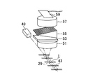
図3はチップデバイスを用いた電気泳動装置に適用された従来の蛍光検出装置を示す斜視図である。
チップデバイス1には複数の分析流路43が形成されており、それらの分析流路43の所定位置に複数の分析流路43にまたがる帯状の検出領域29が設けられている。
チップデバイス1の側方に設けられたレーザ装置49により、検出領域29に励起光が照射されて複数の分析流路43に励起光が同時に照射される。
【0004】
チップデバイス1の上方に設けられた集光レンズ51により、検出領域29内の特定の分析流路43からの光を集光して平行光にする。その平行光を、レーザ光を除去するための除去フィルター53を介して、透過型回折格子55に送る。透過型回折格子55により除去フィルター53からの平行光を分光し、結像レンズ57を介して、CCD(Charge Coupled Device)59に結像する。各波長の光はCCD59の異なる位置に結像される。CCD59の検出信号に基づいて所定の蛍光波長の強度を算出する。蛍光波長の強度を調べることにより、検出領域29におけるその蛍光波長の蛍光を発する蛍光物質の有無を判断できる。
【0005】
図3の蛍光検出装置では、集光レンズ51、除去フィルター53、透過型回折格子55、結像レンズ57及びCCD59を含む光学系又はチップデバイス1を検出領域29方向に移動させることにより、複数の分析流路43について検出領域29で蛍光検出を順次行なう。
【0006】
【発明が解決しようとする課題】
本発明は、検出信号の高いS/Nを実現できる蛍光検出装置を備えた電気泳動装置を提供することを目的とするものである。
【0007】
【課題を解決するための手段】
本発明にかかる電気泳動装置は、分離用流路が形成されたチップデバイスと、表面上に前記チップデバイスを保持するとともに、該チップデバイスの温度を調節するための温調機構を備えたチップデバイス保持台と、前記チップデバイス保持台に保持されたチップデバイス上を覆い、測定用の光が透過する開口を有する泳動チャンバー蓋と、前記泳動チャンバー蓋の上部に配置され、前記チップデバイス保持台に保持されたチップデバイスの検出領域からの光を前記開口を介してスリットの穴に結像する第1の光学系、及び、少なくとも反射型回折格子を備えて前記スリットの穴からの光を分光し、検出素子に結像する第2の光学系を備えた蛍光検出装置と、を備えたものである。
【0008】
第1の光学系により検出領域からの光をスリットの穴に結像する。反射型回折格子を備えた第2の光学系により、スリットの穴からの光を分光し、検出素子に結像する。
反射型回折格子は透過型回折格子に比較して回折効率が高いので、検出素子の検出信号について高いS/Nを実現できる。さらに、反射型回折格子は結像特性がよいので、複数の分析流路にまたがる帯状の検出領域で蛍光検出を行なう場合であっても、クロストークを低減することができる。
また、チップデバイス保持台と泳動チャンバー蓋によって電気泳動動作中のチップデバイスの温度を所定の温度に調節することができる。
【0009】
【発明の実施の形態】
本発明にかかる電気泳動装置の蛍光検出装置において、反射型回折格子として反射型凹面格子を備え、第2の光学系は反射型凹面格子のみによって構成されていることが好ましい。反射型凹面格子を用いることにより、凹面鏡などの光学系を用いることなく、スリットの穴からの光を分光して検出素子に結像することができる。これにより、装置の構成を簡単にすることができる。
【0010】
【実施例】
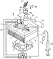
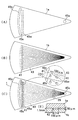
図1は本発明にかかる電気泳動装置の蛍光検出装置の一実施例を備えた電気泳動装置を示す斜視図である。図2は、図1の電気泳動装置に装着される多数の分離用流路が形成されたチップデバイスを表す図であり、(A)は一方の基板の上面図、(B)は他方の基板の上面図、(C)は両基板を重ね合わせた状態での上面図、(D)は(C)の円で囲まれた部分を拡大して示す上面図、(E)は(C)の分析流路部分を示す断面図である。
【0011】
まず、図2に示すチップデバイスについて説明する。
チップデバイス1は、一対の透明板状の無機材料(例えばガラス、石英、シリコンなど)又はプラスチックからなる基板1a,1bにより構成される。基板1a,1bの厚さは1.1mmである。
一方の基板1bの表面には、半導体フォトリソグラフィー技術又はマイクロマシニング技術により、互いに交差するサンプル導入用流路41及び分離用流路43の組が16組形成されている。サンプル導入用流路41及び分離用流路43の寸法は幅が100μm程度、深さが50μm程度である。16組の流路41,43は、他の組の流路と交差しないように、サンプル導入用流路41と交差する側とは反対側の分離用流路43の一端側を要として扇型に配置されている。
【0012】
他方の基板1aには流路41,43の端に対応する位置にアノードリザーバ45a、カソードリザーバ45c、サンプルリザーバ45s、ウエイストリザーバ45wとしての貫通穴が形成されている。リザーバ45s,45wは流路41,43の組ごとに設けられている。アノードリザーバ45aは扇型配置の要側の各組の分離用流路43の一端側で共通である。カソードリザーバ45cは長穴により構成され、各組の分析流路43の他端側で共通である。
図2(D)に示すように、サンプルリザーバ45sからのサンプル導入用流路41とウエイストリザーバ45wからのサンプル導入用流路41は100μmの間隔をもって分析流路43に接続されている。
【0013】
チップデバイス1は、両基板1a,1bを重ねて接合した状態で使用される。チップデバイス1での分離サンプルの検出領域29は、扇型配置の要側の各組の分離用流路43の一端側付近である。
このようなチップデバイスは、多数の分離用流路が形成されていることから、Multi-channel Micro-chipとも呼ばれる。
【0014】
図1を用いて電気泳動装置について説明する。
チップデバイス1はリザーバが形成された表面を上方にしてチップデバイス保持台3に保持されている。チップデバイス保持台3にはチップデバイス1の温度を調節するためのペルチエ式温調機構5が備えられている。ペルチエ式温調機構5に対向する位置にペルチエ式温調機構5に送風するためのファン7が設けられている。チップデバイス保持台3のチップデバイス1が保持された表面を覆う泳動チャンバー蓋9が設けられている。
【0015】
チップデバイス保持台3の付近に、チップデバイス保持台3に保持されたチップデバイス1の流路及びリザーバに泳動媒体としてのポリマーを充填するためのポリマー充填ポート11及びポリマー充填用シリンジ13が設けられている。
チップデバイス保持台3のチップデバイス1が保持された表面側に、チップデバイス1のリザーバ45a,45c,45s,45wに収容された液に電圧を印加するための電極15がリザーバ45a,45c,45s,45wごとに設けられている。各電極15は電極15に電圧を供給するための高電圧供給部17に電気的に接続されている。
【0016】
電気泳動装置の検出装置として蛍光検出装置が備えられている。蛍光検出装置の光源として、励起光源レーザ装置19が設けられている。レーザ装置19としては、例えばアルゴン(Ar)レーザやクリプトン(Kr)レーザ、ヘリウムネオン(He-Ne)レーザ、ネオジム(Nd)-YAG(Y3Al5O12)などのNdイオン固体レーザ、半導体レーザ(Laser Diode:LD)、光第2高調波発生(SHG)現象を利用した固体レーザなど、種々のレーザ装置を用いることができる。
【0017】
レーザ装置19からの励起光の光路にはその励起光を平行光にするビームエキスパンダ21が設けられている。ビームエキスパンダ21からの励起光の光路には、ガルバノミラーやAOD(Acousto-Optics Device)などの励起光を走査するためのビームスキャニング素子23が設けられている。
ビームスキャニング素子23からの励起光の光路には、ビームスキャニング素子23からの励起光をチップデバイス1側へ反射するダイクロイックミラー25が設けられている。ダイクロイックミラー25は励起光を反射し、チップデバイス1側からの蛍光を透過するような波長特性のものを用いる。
【0018】
ダイクロイックミラー25に反射された励起光の光路には、その励起光を泳動チャンバー蓋9に設けられた開口を介してチップデバイス1の分離用流路43の検出領域29(図2も参照)に集光する対物レンズ27が設けられている。
ダイクロイックミラー25の対物レンズ27とは反対側に、励起光成分を除去する除去フィルター31が設けられている。除去フィルター31を透過した蛍光の光路にはその蛍光を、チップデバイス1の検出領域29に対応して長穴が形成されたスリット35に結像するためのレンズ33が設けられている。
【0019】
スリット35の長穴からの蛍光の光路には、その蛍光を分光して冷却CCD39の受光面に結像するための凹面ホログラフィックグレーティング(反射型凹面格子)37が設けられている。
冷却CCD39には、冷却CCD39の動作を制御し、冷却CCD39の検出信号を処理するための演算装置(図示は省略)が電気的に接続されている。
蛍光検出装置は、チップデバイス1の分離用流路43の検出領域29における蛍光を検出して分離したサンプルを検出するものである。グレーティング37により検出領域29からの蛍光を分光することにより、複数種類の蛍光波長を検出することができる。
【0020】
この実施例において、本発明にかかる蛍光検出装置は、励起光源レーザ装置19、ビームエキスパンダ21、ビームスキャニング素子23、ダイクロイックミラー25、対物レンズ27、除去フィルター31、レンズ33、スリット35、グレーティング37及び冷却CCD39により構成され、第1の光学系は、ダイクロイックミラー25、対物レンズ27、除去フィルター31、レンズ33、スリット35により実現され、第2の光学系はグレーティング37により実現されている。
【0021】
図1及び図2を参照してこの電気泳動装置の動作を説明する。
泳動チャンバー蓋9が開けられ、チップデバイス保持台3の所定位置にチップデバイス1が配置された後、ポリマー充填ポート11を移動させてチップデバイス1のリザーバ45aに接合させる。シリンジ13内に収容されたポリマーを押し出して、ポリマー充填ポート11及びリザーバ45aを介して分析流路43及びサンプル導入流路41に充填する。
リザーバ45a,45c,45wにバッファが注入され、サンプルリザーバ45sにサンプルが注入され、各リザーバ45a,45c,45s,45wに電極15が配置された後、泳動チャンバー蓋9が閉じられる。ペルチエ式温調機構5及びファン7を作動させ、チップデバイス1及び泳動チャンバー内を所定の温度に温調する。
【0022】
泳動用高圧電源17により各電極15に所定の電圧を印加してサンプルリザーバ45sに収容されたサンプルをサンプル導入用流路41内に導入した後、各電極15への印加電圧を切り換えて、サンプル導入用流路41と分析流路43の交差部にあるサンプルを分析流路43内に導入する。その後、分析流路43に導入したサンプルをアノードリザーバ45a側へ泳動させて分離させる。
【0023】
励起光源レーザ装置19を作動させ、励起光をビームエキスパンダ21及びビームスキャニング素子23を介してダイクロイックミラー25に照射する。ダイクロイックミラー25により励起光を対物レンズ27側に反射し、対物レンズ27により励起光を検出領域29内に照射する。このとき、ビームスキャニング素子23により、検出領域29内で分析流路43が並ぶ方向(図1中矢印参照)に励起光が走査されるように、ダイクロイックミラー25への励起光の照射位置を走査する。
【0024】
検出領域29からの光を対物レンズ27により集光し、平行光にしてダイクロイックミラー25へ送る。ダイクロイックミラー25は対物レンズ27からの光を透過して除去フィルター31に送る。除去フィルター31はダイクロイックミラー25からの光のうち、励起光成分を除去し、所定の波長の蛍光のみを透過してレンズ33に送る。レンズ33は除去フィルター31からの蛍光をスリット35の長穴に集光する。スリット35の長穴を通過した蛍光はグレーティング37に照射される。グレーティング37はスリット35からの蛍光を分光し、冷却CCD39の受光面に結像する。冷却CCD39の検出信号に基づいて、蛍光標識されたサンプルを検出する。
【0025】
図1に示す一実施例としての蛍光検出装置では、透過型回折格子を用いた従来の蛍光検出装置とは異なり、反射型回折格子である凹面ホログラフィックグレーティング37を用いているので、回折効率がよく、従来の蛍光検出装置に比べて冷却CCD39の検出信号のS/Nを向上させることができる。また、結像特性がよいことから、隣接する分析流路43間のクロストークを低減することができる。
【0026】
図1では、一実施例としての蛍光検出装置を電気泳動装置に適用しているが、本発明はこれに限定されるものではなく、蛍光検出を行なう他の装置にも適用できるし、蛍光検出装置単体として用いることもできる。例えば、サンプルを収容するための複数の凹部が配列されたマイクロタイタープレート用の蛍光検出装置として用いることができる。
【0027】
本発明にかかる蛍光検出装置の構成は図1に示すものに限定されるものではない。すなわち、第1の光学系は検出領域からの光をスリットの穴に結像することができ、第2の光学系は少なくとも反射型回折格子を備え、スリットの穴からの光を分光し、検出素子に結像することができる構成であればどのような構成であってもよい。また、光源を含む励起光を照射する光学系はどのような構成であってもよく、例えば光源としてLED(Light Emitting Diode)を用いてもよい。
【0028】
また、図1に示した蛍光検出装置では、第2の光学系として反射型凹面格子である凹面ホログラフィックグレーティングのみを用いているが、本発明を構成する第2の光学系はこれに限定されるものではなく、凹面鏡と反射型平面格子の組み合わせであってもよい。
また、図1に示した蛍光検出装置では、検出領域に励起光を照射する光学系として、ビームスキャニング素子を用いて検出領域内で励起光を走査するものを用いているが、本発明はこれに限定されるものではなく、検出領域内にライン状の励起光を照射する光学系や、チップデバイスの側面から検出領域に励起光を照射する光学系など、検出領域に励起光を照射できる光学系であればどのような光学系であってもよい。
【0029】
【発明の効果】
本発明の電気泳動装置の蛍光検出装置では、検出領域からの光をスリットの穴に結像する第1の光学系と、少なくとも反射型回折格子を備え、スリットの穴からの光を分光し、検出素子に結像する第2の光学系とを備え、透過型回折格子に比較して回折効率が高い反射型回折格子により検出領域からの光を分光するようにしたので、検出素子の検出信号について高いS/Nを実現できる。さらに、複数の検出位置にまたがる検出領域で蛍光検出を行なう場合であっても、反射型回折格子の高い結像特性により、クロストークを低減することができる。
また、チップデバイス保持台が温調機構を備え、泳動チャンバー蓋によってチップデバイス上を覆ったので、電気泳動動作中のチップデバイスの温度を所定の温度に調節することができる。
【0030】
本発明にかかる蛍光検出装置において、反射型回折格子として反射型凹面格子を備え、第2の光学系は反射型凹面格子のみによって構成されているようにすれば、装置の構成を簡単にすることができる。
【図面の簡単な説明】
【図1】本発明にかかる蛍光検出装置の一実施例を備えた電気泳動装置を示す斜視図である。
【図2】図1の電気泳動装置に装着されるチップデバイスを表す図であり、(A)は一方の基板の上面図、(B)は他方の基板の上面図、(C)は両基板を重ね合わせた状態での上面図、(D)は(C)の円で囲まれた部分を拡大して示す上面図、(E)は(C)の分析流路部分を示す断面図である。
【図3】チップデバイスを用いた電気泳動装置に適用された従来の蛍光検出装置を示す斜視図である。
【符号の説明】
1 チップデバイス
3 チップデバイス保持台
5 ペルチエ式温調機構
7 ファン
9 泳動チャンバー蓋
11 ポリマー充填ポート
13 ポリマー充填用シリンジ
15 電極
17 高電圧供給部
19 励起光源レーザ装置
21 ビームエキスパンダ
23 ビームスキャニング素子
25 ダイクロイックミラー
27 対物レンズ
29 検出領域
31 除去フィルター
33 レンズ
35 スリット
37 凹面ホログラフィックグレーティング(反射型凹面格子)
39 冷却CCD[0001]
BACKGROUND OF THE INVENTION
The present invention relates to an electrophoresis apparatus that includes a fluorescence detection device that detects fluorescence in a detection region, and analyzes, for example, a very small amount of protein, nucleic acid, drug, and the like at high speed and with high resolution.
[0002]
[Prior art]
In the case of analyzing a very small amount of protein or nucleic acid, an electrophoresis apparatus has been conventionally used. Examples of the electrophoresis apparatus include those using a glass capillary having an inner diameter of 100 μm or less and those using a chip device in which a groove having a width of about 100 μm and a depth of about 50 μm is formed in a substrate. For detection with an electrophoresis apparatus, a sample is generally fluorescently labeled in advance, and a fluorometric method is generally used.
[0003]
FIG. 3 is a perspective view showing a conventional fluorescence detection apparatus applied to an electrophoresis apparatus using a chip device.
A plurality of
A
[0004]
By the
[0005]
In the fluorescence detection apparatus of FIG. 3, a plurality of optical systems or
[0006]
[Problems to be solved by the invention]
An object of the present invention is to provide an electrophoresis apparatus including a fluorescence detection apparatus that can realize a high S / N ratio of a detection signal.
[0007]
[Means for Solving the Problems]
An electrophoresis apparatus according to the present invention includes a chip device having a separation channel formed thereon, and a chip device having a temperature control mechanism for holding the chip device on the surface and adjusting the temperature of the chip device. A holding table, an electrophoresis chamber lid that covers the chip device held on the chip device holding table and has an opening through which light for measurement is transmitted; and an upper portion of the electrophoresis chamber lid, the chip device holding table A first optical system that forms an image of light from the detection region of the held chip device in the slit hole through the opening; and at least a reflective diffraction grating; and the light from the slit hole is dispersed. And a fluorescence detection apparatus including a second optical system that forms an image on the detection element.
[0008]
The light from the detection region is imaged in the hole of the slit by the first optical system. The light from the slit hole is dispersed by the second optical system provided with the reflective diffraction grating and imaged on the detection element.
Since the reflection type diffraction grating has a higher diffraction efficiency than the transmission type diffraction grating, a high S / N can be realized for the detection signal of the detection element. Furthermore, since the reflection type diffraction grating has good imaging characteristics, crosstalk can be reduced even when fluorescence detection is performed in a band-shaped detection region extending over a plurality of analysis channels.
Further, the temperature of the chip device during the electrophoresis operation can be adjusted to a predetermined temperature by the chip device holding base and the electrophoresis chamber lid.
[0009]
DETAILED DESCRIPTION OF THE INVENTION
In the fluorescence detection device of the electrophoretic device according to the present invention, it is preferable that a reflective concave grating is provided as the reflective diffraction grating, and the second optical system is constituted only by the reflective concave grating. By using a reflective concave grating, light from the slit hole can be dispersed and imaged on the detection element without using an optical system such as a concave mirror. Thereby, the configuration of the apparatus can be simplified.
[0010]
【Example】
FIG. 1 is a perspective view showing an electrophoresis apparatus provided with an embodiment of a fluorescence detection apparatus of an electrophoresis apparatus according to the present invention. 2A and 2B are diagrams showing a chip device in which a large number of separation flow paths are formed, which are mounted on the electrophoresis apparatus of FIG. 1, wherein FIG. 2A is a top view of one substrate, and FIG. 2B is the other substrate. (C) is a top view in a state in which both substrates are overlapped, (D) is a top view showing an enlarged portion surrounded by a circle in (C), and (E) is a view in (C). It is sectional drawing which shows an analysis flow path part.
[0011]
First, the chip device shown in FIG. 2 will be described.
The
On the surface of one
[0012]
On the
As shown in FIG. 2D, the
[0013]
The
Such a chip device is also called a multi-channel micro-chip because a large number of separation channels are formed.
[0014]
The electrophoresis apparatus will be described with reference to FIG.
The
[0015]
In the vicinity of the chip device holding table 3, a
On the surface side of the chip device holding table 3 on which the
[0016]
A fluorescence detection device is provided as a detection device of the electrophoresis apparatus. An excitation light
[0017]
A
A
[0018]
In the optical path of the excitation light reflected by the
A
[0019]
A concave optical holographic grating (reflective concave grating) 37 is provided in the optical path of the fluorescent light from the long hole of the
The cooling
The fluorescence detection apparatus detects a separated sample by detecting fluorescence in the
[0020]
In this embodiment, the fluorescence detection apparatus according to the present invention includes an excitation light
[0021]
The operation of this electrophoresis apparatus will be described with reference to FIGS.
After the
A buffer is injected into the
[0022]
A predetermined voltage is applied to each
[0023]
The excitation light
[0024]
The light from the
[0025]
Unlike the conventional fluorescence detection apparatus using a transmission type diffraction grating, the fluorescence detection apparatus as an embodiment shown in FIG. 1 uses a concave
[0026]
In FIG. 1, the fluorescence detection apparatus as an embodiment is applied to an electrophoresis apparatus. However, the present invention is not limited to this, and can be applied to other apparatuses that perform fluorescence detection. It can also be used as a single device. For example, it can be used as a fluorescence detection device for a microtiter plate in which a plurality of recesses for accommodating a sample are arranged.
[0027]
The configuration of the fluorescence detection apparatus according to the present invention is not limited to that shown in FIG. That is, the first optical system can image the light from the detection region on the slit hole, and the second optical system includes at least a reflective diffraction grating, and spectrally detects and detects the light from the slit hole. Any configuration may be used as long as an image can be formed on the element. Further, the optical system that irradiates the excitation light including the light source may have any configuration. For example, an LED (Light Emitting Diode) may be used as the light source.
[0028]
In the fluorescence detection apparatus shown in FIG. 1, only the concave holographic grating, which is a reflective concave grating, is used as the second optical system. However, the second optical system constituting the present invention is not limited to this. It may be a combination of a concave mirror and a reflective planar grating.
In the fluorescence detection apparatus shown in FIG. 1, the optical system for irradiating the detection area with the excitation light uses an optical system that scans the excitation light within the detection area using a beam scanning element. The optical system that can irradiate the detection region with excitation light, such as an optical system that irradiates the detection region with line-shaped excitation light, or an optical system that irradiates the detection region with the excitation light from the side of the chip device. Any optical system may be used.
[0029]
【The invention's effect】
In the fluorescence detection device of the electrophoresis apparatus of the present invention, the first optical system that forms an image of light from the detection region on the hole of the slit, and at least a reflective diffraction grating, and spectrally separates the light from the hole of the slit, And a second optical system that forms an image on the detection element, and the light from the detection region is spectrally separated by the reflection type diffraction grating having higher diffraction efficiency than the transmission type diffraction grating. High S / N can be realized. Furthermore, even when fluorescence detection is performed in a detection region extending over a plurality of detection positions, crosstalk can be reduced due to the high imaging characteristics of the reflective diffraction grating.
In addition, since the chip device holding base includes a temperature control mechanism and the chip device is covered with the electrophoresis chamber lid, the temperature of the chip device during the electrophoresis operation can be adjusted to a predetermined temperature.
[0030]
In the fluorescence detection apparatus according to the present invention, if a reflection type concave grating is provided as a reflection type diffraction grating, and the second optical system is constituted only by the reflection type concave grating, the structure of the apparatus can be simplified. Can do.
[Brief description of the drawings]
FIG. 1 is a perspective view showing an electrophoresis apparatus provided with an embodiment of a fluorescence detection apparatus according to the present invention.
2A and 2B are diagrams illustrating a chip device mounted on the electrophoresis apparatus of FIG. 1, wherein FIG. 2A is a top view of one substrate, FIG. 2B is a top view of the other substrate, and FIG. FIG. 4D is a top view in a state where the two are superposed, FIG. 4D is an enlarged top view showing a portion surrounded by a circle in FIG. 2C, and FIG. 3E is a cross-sectional view showing the analysis flow path portion in FIG. .
FIG. 3 is a perspective view showing a conventional fluorescence detection apparatus applied to an electrophoresis apparatus using a chip device.
[Explanation of symbols]
DESCRIPTION OF
39 Cooling CCD
Claims (2)
表面上に前記チップデバイスを保持するとともに、該チップデバイスの温度を調節するための温調機構を備えたチップデバイス保持台と、
前記チップデバイス保持台に保持されたチップデバイス上を覆い、測定用の光が透過する開口を有する泳動チャンバー蓋と、
前記泳動チャンバー蓋の上部に配置され、前記チップデバイス保持台に保持されたチップデバイスの検出領域からの光を前記開口を介してスリットの穴に結像する第1の光学系、及び、少なくとも反射型回折格子を備えて前記スリットの穴からの光を分光し、検出素子に結像する第2の光学系を備えた蛍光検出装置と、
を備えたことを特徴とする電気泳動装置。A chip device in which a separation channel is formed;
A chip device holding stand having a temperature control mechanism for holding the chip device on the surface and adjusting the temperature of the chip device;
An electrophoresis chamber lid that covers the chip device held on the chip device holding table and has an opening through which light for measurement is transmitted;
A first optical system which is disposed on the upper part of the electrophoresis chamber lid and forms an image of light from a detection region of the chip device held by the chip device holding table in the slit hole through the opening; and at least the reflection A fluorescence detection device including a second optical system that includes a second diffraction grating and diffracts light from the slit hole and forms an image on a detection element;
An electrophoretic device comprising:
Priority Applications (4)
| Application Number | Priority Date | Filing Date | Title |
|---|---|---|---|
| JP2000393381A JP3636070B2 (en) | 2000-12-25 | 2000-12-25 | Electrophoresis device |
| US09/982,964 US7033475B2 (en) | 2000-10-25 | 2001-10-22 | Electrophoretic apparatus |
| KR10-2001-0065645A KR100491857B1 (en) | 2000-10-25 | 2001-10-24 | Electrophoretic apparatus |
| CN01136660A CN1350179A (en) | 2000-10-25 | 2001-10-25 | Electrophoresis appareatus |
Applications Claiming Priority (1)
| Application Number | Priority Date | Filing Date | Title |
|---|---|---|---|
| JP2000393381A JP3636070B2 (en) | 2000-12-25 | 2000-12-25 | Electrophoresis device |
Publications (2)
| Publication Number | Publication Date |
|---|---|
| JP2002195949A JP2002195949A (en) | 2002-07-10 |
| JP3636070B2 true JP3636070B2 (en) | 2005-04-06 |
Family
ID=18859197
Family Applications (1)
| Application Number | Title | Priority Date | Filing Date |
|---|---|---|---|
| JP2000393381A Expired - Lifetime JP3636070B2 (en) | 2000-10-25 | 2000-12-25 | Electrophoresis device |
Country Status (1)
| Country | Link |
|---|---|
| JP (1) | JP3636070B2 (en) |
Families Citing this family (6)
| Publication number | Priority date | Publication date | Assignee | Title |
|---|---|---|---|---|
| US7724298B2 (en) * | 2003-10-09 | 2010-05-25 | Sony Corporation | Image processing system and method for pick up and display of an object including division of an optical image of the object into a spectrum |
| KR100647317B1 (en) * | 2005-02-03 | 2006-11-23 | 삼성전자주식회사 | Optical system for measuring multi-channel fluorescence and multi-channel fluorescence sample analyzer |
| JP4720419B2 (en) * | 2005-10-11 | 2011-07-13 | 株式会社島津製作所 | Separation buffer solution filling apparatus for microchip and microchip processing apparatus having the same |
| JP4525725B2 (en) | 2007-10-18 | 2010-08-18 | ソニー株式会社 | OPTICAL MEASUREMENT UNIT, OPTICAL MEASUREMENT MEMBER, FINE PARTICLE MEASUREMENT DEVICE PROVIDED WITH THE SAME, AND MICROPARTICLE OPTICAL MEASUREMENT METHOD |
| US9778166B2 (en) | 2014-02-24 | 2017-10-03 | National University Corporation Kagawa University | Microparticle measurement device |
| KR101861919B1 (en) * | 2016-06-16 | 2018-05-28 | 한국과학기술원 | Rapid optical inspection method of semiconductor |
-
2000
- 2000-12-25 JP JP2000393381A patent/JP3636070B2/en not_active Expired - Lifetime
Also Published As
| Publication number | Publication date |
|---|---|
| JP2002195949A (en) | 2002-07-10 |
Similar Documents
| Publication | Publication Date | Title |
|---|---|---|
| JP5145309B2 (en) | Optical alignment device for capillary electrophoresis apparatus | |
| US7670770B2 (en) | Nanochannel arrays and their preparation and use for high throughput macromolecular analysis | |
| US6905583B2 (en) | Closed-loop control of electrokinetic processes in microfluidic devices based on optical readings | |
| US7033475B2 (en) | Electrophoretic apparatus | |
| US6759662B1 (en) | Optical detection system | |
| US6900889B2 (en) | Submersible light-directing member for material excitation in microfluidic devices | |
| JP3783826B2 (en) | Biochip reader | |
| JP5076204B2 (en) | Method and apparatus for fluorescence detection in confocal scanning microscopy | |
| US20020117398A1 (en) | Capillary electrophoretic apparatus | |
| JP4489479B2 (en) | Rotating confocal scanner for capillary array detection | |
| JP2005526252A (en) | Optical instrument with excitation source | |
| PT1354192E (en) | Multi-channel bio-separation cartridge | |
| US20170343509A1 (en) | Nanochannel arrays and their preparation and use for high throughput macromolecular analysis | |
| JP2005501249A (en) | Multi-channel analyte separation device using side-incidence excitation | |
| JP3636070B2 (en) | Electrophoresis device | |
| JP2007163488A (en) | Multicapillary electrophoretic fluorescence system | |
| US20110207207A1 (en) | Microfluidic cell sorter utilizing broadband coherent anti-stokes raman scattering | |
| US7118662B2 (en) | Electrophoresis apparatus | |
| JP2003043371A (en) | Method for scanning region of interest(roi) by high time resolution | |
| JP4321910B2 (en) | Multi-capillary electrophoresis device | |
| US8545686B2 (en) | Electrophoretic apparatus and electrophoretic method | |
| JP4679375B2 (en) | Capillary electrophoresis device | |
| JP4438211B2 (en) | Electrophoresis device | |
| JP2006292369A (en) | Capillary electrophoresis apparatus and capillary electrophoresis method | |
| JP2006105881A (en) | Electrophoresis device |
Legal Events
| Date | Code | Title | Description |
|---|---|---|---|
| A977 | Report on retrieval |
Free format text: JAPANESE INTERMEDIATE CODE: A971007 Effective date: 20040324 |
|
| A131 | Notification of reasons for refusal |
Free format text: JAPANESE INTERMEDIATE CODE: A131 Effective date: 20040406 |
|
| A521 | Written amendment |
Free format text: JAPANESE INTERMEDIATE CODE: A523 Effective date: 20040607 |
|
| TRDD | Decision of grant or rejection written | ||
| A01 | Written decision to grant a patent or to grant a registration (utility model) |
Free format text: JAPANESE INTERMEDIATE CODE: A01 Effective date: 20041214 |
|
| A61 | First payment of annual fees (during grant procedure) |
Free format text: JAPANESE INTERMEDIATE CODE: A61 Effective date: 20041227 |
|
| R150 | Certificate of patent or registration of utility model |
Free format text: JAPANESE INTERMEDIATE CODE: R150 Ref document number: 3636070 Country of ref document: JP Free format text: JAPANESE INTERMEDIATE CODE: R150 |
|
| FPAY | Renewal fee payment (event date is renewal date of database) |
Free format text: PAYMENT UNTIL: 20080114 Year of fee payment: 3 |
|
| FPAY | Renewal fee payment (event date is renewal date of database) |
Free format text: PAYMENT UNTIL: 20090114 Year of fee payment: 4 |
|
| FPAY | Renewal fee payment (event date is renewal date of database) |
Free format text: PAYMENT UNTIL: 20100114 Year of fee payment: 5 |
|
| FPAY | Renewal fee payment (event date is renewal date of database) |
Free format text: PAYMENT UNTIL: 20100114 Year of fee payment: 5 |
|
| FPAY | Renewal fee payment (event date is renewal date of database) |
Free format text: PAYMENT UNTIL: 20110114 Year of fee payment: 6 |
|
| FPAY | Renewal fee payment (event date is renewal date of database) |
Free format text: PAYMENT UNTIL: 20120114 Year of fee payment: 7 |
|
| FPAY | Renewal fee payment (event date is renewal date of database) |
Free format text: PAYMENT UNTIL: 20130114 Year of fee payment: 8 |
|
| FPAY | Renewal fee payment (event date is renewal date of database) |
Free format text: PAYMENT UNTIL: 20140114 Year of fee payment: 9 |
|
| EXPY | Cancellation because of completion of term |