JP3632443B2 - Semiconductor device - Google Patents
Semiconductor device Download PDFInfo
- Publication number
- JP3632443B2 JP3632443B2 JP14709498A JP14709498A JP3632443B2 JP 3632443 B2 JP3632443 B2 JP 3632443B2 JP 14709498 A JP14709498 A JP 14709498A JP 14709498 A JP14709498 A JP 14709498A JP 3632443 B2 JP3632443 B2 JP 3632443B2
- Authority
- JP
- Japan
- Prior art keywords
- refresh
- control signal
- self
- signal
- circuit
- Prior art date
- Legal status (The legal status is an assumption and is not a legal conclusion. Google has not performed a legal analysis and makes no representation as to the accuracy of the status listed.)
- Expired - Fee Related
Links
Images


Description
【0001】
【発明の属する技術分野】
本発明は、リフレッシュが必要なメモリ、つまりダイナミックランダムアクセスメモリ(以下、DRAMと略す)とロジック回路とが1チップ化された半導体装置に関するものである。
【0002】
【従来の技術】
メモリセルがコンデンサによって形成されているDRAMにおいては、ある時間経つと、電荷としてメモリセルに保持されているデータがリーク電流により失われてしまう。したがって、メモリセルが保持するデータを書き直して維持するために、リフレッシュ動作を行う必要がある。DRAMにおけるリフレッシュ動作は、メモリセルが有するそれぞれ複数の行と列とにより構成されたメモリマトリクスにおいて、1行分の行線(ワード線)を選択した後にそのワード線上のすべてのメモリセルについて読み出し・増幅・再書き込みを行う動作を、全ワード線に対して順次行うことにより実現される。
【0003】
DRAMのリフレッシュ動作としては、メモリセルに対するデータの読み出し/書き込みといったランダムアクセス動作中に割り込んで行われるリフレッシュ動作と、DRAMがランダムアクセス動作中でなくデータ保持モードである期間、例えば電池によるバックアップ期間中に行われるリフレッシュ動作とがある。
【0004】
前者、つまりアクセス動作中に割り込んで行われるリフレッシュ動作には2つの方式がある。1つは、リフレッシュ用の行アドレスを外部のリフレッシュアドレスカウンタから与え、行アドレスストローブ信号/RASを立ち下げてから立ち上げるまでの期間にリフレッシュを行う、RASオンリリフレッシュ方式である。もう1つは、外部からリフレッシュ要求信号を与え、行アドレスを外部アドレスからDRAM内蔵のリフレッシュアドレスカウンタへ切り換えてリフレッシュを行う、オートリフレッシュ方式である。現在、オートリフレッシュ方式としては、列アドレスストローブ信号/CAS、行アドレスストローブ信号/RASの順にLowレベル“L”にし、かつ、行アドレスストローブ信号/RASを立ち下げてから立ち上げるまでの間にリフレッシュを行う、CASビフォアRASリフレッシュ(以下、CBRリフレッシュと略す)が標準仕様になっている。
【0005】
後者、つまりデータ保持モードにおけるリフレッシュ動作には、内部のタイマーが自動的に生成したリフレッシュ要求信号に応じて、内蔵したリフレッシュアドレスカウンタの出力を行アドレスとしてリフレッシュを行うことにより、外部から制御信号を与えなくても一定の周期でリフレッシュを継続して行うセルフリフレッシュ方式がある。現在、セルフリフレッシュ方式としては、CBRリフレッシュにおいて行アドレスストローブ信号/RAS及び列アドレスストローブ信号/CASの双方を“L”のまま100μsec以上保つことによりセルフリフレッシュ動作に入る、CBRセルフリフレッシュが標準仕様になっている。
【0006】
【発明が解決しようとする課題】
しかしながら、上記従来の構成によれば、セルフリフレッシュ時のリフレッシュ要求信号を生成するセルフリフレッシュ回路のチェックするための信号を外部端子に出力していないため、セルフリフレッシュ回路の不良を検出するために、メモリにデータを書き込んでから、セルフリフレッシュモードに入り、リフレッシュしなければメモリセルに保持されているデータがリークして失われてしまう時間以上待った後、メモリセルのデータを読んで、データが失なわれたかどうかのテストを行っており、テスト時間が長くなるという課題と前記リフレッシュ要求信号のパルス幅をチェックできないのとセルフリフレッシュ時のリフレッシュ周期のチェックできないので、トリミングによるリフレッシュ周期の最適化ができないという課題と前記パルス幅またはリフレッシュ周期が規格外の時にトリミングにより前記パルス幅または周期を規格内にすることができないという課題とを有していた。本発明は、上記従来の問題に鑑み、リフレッシュが必要なメモリ、つまりDRAMとロジック回路とが1チップ化された半導体装置であって、前記セルフリフレッシュ回路のテストを短時間で行うことができ、トリミングによるセルフリフレッシュ周期の最適化及び不良品の救済を行うことができる半導体装置を提供することを目的とする。
【0007】
【課題を解決するための手段】
この課題を解決するために本発明の半導体装置は、データを記憶するためのリフレッシュが必要なメモリセルを有するメモリと、セルフリフレッシュ制御信号が入力されると、一定の周期を有する発振クロックを供給するための発振手段と、前記発振クロックに基づいて、前記メモリセルをリフレッシュするための内部セルフリフレッシュ制御信号を供給するための信号生成手段と、セルフリフレッシュテスト時には、前記内部セルフリフレッシュ制御信号に基づいて行選択制御信号を供給し、メモリからのデータ読み出しテスト時には、外部入力端子からの入力に基づいて前記行選択制御信号を供給する論理ゲート回路と、前記行選択制御信号に応答して行アドレスにより選択されたワード線を活性化する行選択回路と、前記行選択制御信号を外部端子に出力する信号出力手段とを備えることにより、セルフリフレッシュ時のリフレッシュ周期をチェックすることができるようにした。
【0008】
これにより、前記セルフリフレッシュ回路のテストを短時間で行うことができ、トリミングによるセルフリフレッシュ周期の最適化及び不良品の救済を行うことができる半導体装置を実現することができた。
【0009】
【発明の実施の形態】
以下、本発明の実施の形態1の半導体装置について図面を参照しながら説明する。
【0010】
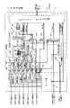
図1は本発明の実施の形態1における半導体装置の構成を示すものである。
図1において、メモリセル及び周辺回路3は、複数のメモリセルで構成されたメモリアレイとその周辺回路で構成されたブロック、ロジック部4は、マイコン又はロジックで構成されたブロック、リフレッシュカウンタ224は、リフレッシュ時の行アドレスを生成するためのカウンタ回路、210〜214、230、231はインバータ回路、215〜218はDフリップフロップ(以下DFFと略す)、セレクタ201〜208、229は、S入力が“H”の場合に、B入力が選択される。行アドレスラッチ225、列アドレスラッチ226、バイトアドレスラッチ227は、EN入力が、“H”の場合にクロック(2)の立ち上がりで入力信号をラッチする回路である。テストデコード回路228は、複数本の外部テスト入力端子をデコードして、DRAM2のテストモードを決定する回路である。
【0011】
図2は、図1のメモリセルアレイ及び周辺回路3の構成図である。メモリセルM01〜MN2mは、容量に1ビット分のデータを記憶するための記憶素子である。メモリセルアレイ300は、N行×2m列のメモリセルM01〜MN2mを有する記憶手段である。そして、メモリセルアレイ300は、N本の行選択線であるワード線WL1〜Nと、2mペアのビット対線であるビット線(1)〜2m、/ビット線(1)〜2mによりデータの読み書きが実行される構成を有する。行選択回路301は、行選択制御信号を受け取り、かつ、受け取った行アドレスに基づいてワード線WLを選択して、選択されたワード線WLにパルスを印加するための行選択手段である。センスアンプSA1〜2mは、ビット線,/ビット線間の微小な電圧差を増幅するための増幅手段、PchトランジスタT01〜T0(2m)、T11〜T1(2m)は、行選択制御信号に応じてビット線,/ビット線へプリチャージ電圧を印加して、各ビット線、/ビット線をプリチャージするためのスイッチング手段である。PchトランジスタT21〜T2(2m)は、行選択制御信号に応じて各ビット線、/ビット線をイコライズするためのスイッチング手段である。NchのトランスファーゲートTG01〜TG0(2m)、TG11〜TG1(2m)は、センスアンプで増幅されたビット線,/ビット線をメインアンプMA0〜MAのメインビット線、/メインビット線に接続するためのスイッチング手段である。
【0012】
図3は、図1のセルフリフレッシュ回路250の詳細説明図である。
図3において、発振回路251は、受け取ったセルフリフレッシュ制御信号が“H”の場合には、クロックCLK1を供給するための発振手段である。2分周器268,269,270は、受け取ったクロックCLK1を順次分周し、それぞれ分周クロックCLK2,CLK4,CLK8を供給するための分周手段である。セレクタ271は、クロック選択信号が、”H”の場合には、分周クロックCLK8を選択して、クロック選択信号が、”L”の場合には、分周クロックCLK8を選択して、分周信号CKOを供給するための選択手段である。1ショットパルス発生回路274は、受け取った分周信号CKOの立ち上がりに応じて、所定のパルス幅を有するセットパルスSETPを生成するためのパルス生成手段である。セットリセット回路275は、それぞれ受け取ったセットパルスSETPとリセットパルスRSTPとに応じて、セルフリフレッシュ信号SROを供給するための信号生成手段である。
【0013】
第1の遅延回路276は、受け取った内部セルフリフレッシュ信号を一定時間遅延させたリセットパルスRSTPを、セットリセット回路275のリセット端子に供給するための遅延手段である。
【0014】
以下、第1の実施の形態である半導体装置1に内蔵されたDRAM2のデータ読み出しテスト時の動作を説明する。テスト時は、外部入力端子より信号を入力して、DRAM2を単体でテストする。
【0015】
まず、データ読み出しテスト時の入力信号の選択動作について、図1を用いて説明する。図1において、外部テスト入力端子によりデータ読み出しテストのモードに設定されるとテストデコード回路228により、DRAMテスト信号が、Highレベルに設定されるため、セレクタ201〜セレクタ208でB入力が選択される。従って、クロック(2)には、外部入力端子(1)が入力され、/セルフリフレッシュ制御信号(2)には、外部入力端子(2)が入力され、/オートリフレッシュ制御信号(2)には、外部入力端子(3)が入力され、/行選択制御信号(2)には、外部入力端子(4)が入力され、/列選択制御信号(2)には、外部入力端子(5)が入力され、/ライト制御信号(2)には外部入力端子(6)が入力され、行アドレス2と列アドレス(2)には共に外部入力端子(7)が入力される。
【0016】
ここで、DRAMのアドレス入力として、行アドレス(2)及び列アドレス(2)は共に外部入力端子(7)からの入力となるが、これはテスト時の外部端子数を減らすために共用しているものであり、行アドレスと列アドレスを多重化した信号を外部入力端子(7)に与え、DRAM2内で行アドレスと列アドレスに分離している。
【0017】
図1及び図2及び図4のタイミングチャートを使ってDRAM2のテスト時の読み出し動作を説明する。
【0018】
DRAM2のデータ読み出しテスト時のページモードでの読み出し動作について、図4のタイミングチャート及び図1、図2を参照して説明する。図4の時間t0において、/セルフリフレッシュ制御信号(2)がHighレベルであるので、後述するがセルフリフレッシュ回路の出力である内部セルフリフレッシュ制御信号は、Lowレベル、/オートリフレッシュ制御信号(2)を図1のDFF215によりクロック(2)で同期化した信号内部オートリフレッシュ制御信号がLowレベル、/行選択制御信号(2)を図1のDFF216によりクロック(2)で同期化した信号内部行選択制御信号がLowレベルであるため、OR回路222の出力である行選択制御信号がLowレベルになり、PchトランジスタT01〜T0(2m)、T11〜T1(2m)、T21〜T2(2m)がONして、ビット線(1)〜2m、/ビット線(1)〜2mが1/2Vddにプリチャージ、イコライズされる。
【0019】
図4の時間t1において、行選択制御信号(2)がHighレベルよりLowレベルに立ち下がると、行選択制御信号がLowレベルよりHighレベルに立ち上がり、PchトランジスタT01〜T0(2m)、T11〜T1(2m)、T21〜T2(2m)がOFFして、ビット線(1)〜2m、/ビット線(1)〜2mのプリチャージ、イコライズが停止され、時間t1のクロック(2)の立ち上がりで、インバータ214の出力信号である行アドレスラッチ225のラッチイネーブル信号がHighレベルであるため、行アドレスラッチ225は、行アドレス(2)をクロック(2)によりラッチし、行アドレスを出力する。内部セルフリフレッシュ制御信号、内部オートリフレッシュ制御信号がLowレベルであるので、NOR回路221の出力である/内部リフレッシュ制御信号がHighレベルになり、セレクタ229のB入力である行アドレス(3)が選択され、行アドレスに出力される。
【0020】
図2において、行選択回路301は、行選択制御信号がHighレベルなので、行アドレスにより選択された行線WLnがHighレベルになり、遅延回路(2)−303によりセンスアンプイネーブルが、時間t1より遅延してHighレベルになり、センスアンプSA1〜SA2mが活性化され、WLnに接続されたメモリセルのデータが、ビット線(1)〜2m、/ビット線(1)〜2mに読み出されて、センスアンプSA1〜SA2mで差動増幅される。
【0021】
/内部リフレッシュ制御信号がHighレベルのため行選択制御信号がHighレベルになり、本実施の形態では、行アドレスの中の1ビットである行アドレス(0)をLowレベルとするため、AND回路306の出力であるゲートイネーブル(0)が図4に示したように、行選択制御信号の立ち上がりより、遅延回路(3)−304の遅延時間遅れてHighレベルになり、AND回路307の出力であるゲートイネーブル(1)がLowレベルであるため、奇数番目のトランジスタTG01、TG11、TG03、TG13、TG05、TG15・・・・・TG0(2m−1)、TG1(2m−1)がオンして、奇数番目のセンスアンプS1、S3、S5・・・・・S(2m−1)の出力がメインアンプMA1〜MAmに入力され、センスアンプの出力であるメインビット線と/メインビット線の電圧の差が大きくなった時点で、メインアンプMA1〜MAmの差動増幅が開始して、図4に示したようにメインアンプMA1〜MAmよりMOUT1〜MOUTmが出力される。
【0022】
時間t2において、行選択制御信号(2)、列選択制御信号(2)ともLowレベルのため、図1のインバータ211、212の出力がHighレベルになるため、ANDゲート219の出力がHighレベルになるため、列アドレスラッチ226がラッチイネーブルになり、時間t2において、クロックの立ち上がりで列アドレス(2)がラッチされ、列アドレスが出力される。同じように、バイトアドレスラッチ227もクロックの立ち上がりでバイトアドレス(1)をラッチして、バイトアドレスを出力する。図2に示したように、列選択回路302で、MOUT1〜MOUTmのmビットのデータより列アドレス(3)により、選択された8kビットのデータ出力信号がデータ選択回路308に出力され、データ選択回路308により、8kビットのデータ出力信号の中からバイトアドレスにより8ビットのテストデータが選択されて、テストデータ(7:0)として出力される。前記テストデータ(7:0)のうちテストデータ(7:1)は、セレクタ309に出力され、テストデータ(0)は、セレクタ312に出力される。DRAMテスト信号が、Highレベルのため、インバータ314の出力がLowレベルになるため、セレクタ309はA入力であるテストデータ(7:1)が、トライステートバッファ310に出力される。時間t2において、/行選択制御信号(2)及び/列選択制御信号(2)がLowレベル、/ライト制御信号2がHighレベルであるからAND回路220がHighレベルになるため、前記AND回路220の出力とクロック(2)によりタイミング生成回路223は、図4に示したようなタイミングで出力制御信号をHighレベルにする。出力制御信号がHighレベル、インバータ314の出力がLowレベルであるためOR回路315の出力であるIO制御信号(1)がHighレベルになり、テストデータ(7:1)が外部入出力端子(7:1)に出力される。
【0023】
セルフテスト信号がLowレベルのため、セレクタ312はA入力であるテストデータ(0)をセレクタ313に出力する。インバータ314の出力がLowレベルになるため、セレクタ313はA入力であるセレクタ312の出力であるテストデータ(0)をトライステートバッファ317に出力する。前述したように、IO制御信号(1)がHighレベル、セルフテスト信号がLowレベルのためOR回路316の出力であるIO制御信号(0)がHighレベルになるため、テストデータ(0)が外部入出力端子(0)に出力される。テストデータ(7:0)は、外部入出力端子(7:0)に図4に示したようなタイミングで出力される。
【0024】
時間t3、t4、t5においても時間t2の時と同じようにクロック(2)の立ち上がりにおいて、/行選択制御信号(2)及び/列選択制御信号(2)ともLowレベルであり、/ライトイネーブル信号がHighレベルであるから、前述したようにクロックの立ち上がりで、ラッチした列アドレスとバイトアドレスで選択されたメモリセルのデータを図4のタイミングチャートに示したように順番に外部入出力端子(7:0)に読み出す。時間t6において、/行選択制御信号(2)及び/列選択制御信号(2)がHighレベルのため、AND回路220の出力がLowレベルになるため出力制御信号がLowレベルになり、IO制御信号(0),(1)がLowレベルになるため、外部入出力端子(7:0)の出力が、ハイインピーダンスになる。
【0025】
次に、セルフリフレッシュ動作をテストするためのセルフテスト時の動作を以下に説明する。まず、図3のセルフリフレッシュ回路の動作を図5のタイミングチャートを使って説明する。
【0026】
時刻0〜t0の期間において、外部入力端子により、/行選択制御信号(2)、/オートリフレッシュ制御信号(2)を“H”に初期設定し、かつ、/セルフリフレッシュ制御信号(2)を“H”にして供給すると、セルフリフレッシュ制御信号が“H”になり、NAND回路257の一方の入力が“L”になるのでその出力である信号S4が“H”に、かつPMOSトランジスタ254がONしてインバータ11の入力である信号S1が“H”になる。したがって、発振用コンデンサ259、260の両端の信号S0と信号S3とが強制的に“H”、つまり電源電圧Vddに初期化されて発振が停止される。また、セルフリフレッシュ制御信号が“L”なので、2分周器268,269、270の出力である分周クロックCLK2,CLK4、CLK8はいずれも“L”に初期化される。
【0027】
ここで、時刻t0において、外部入力端子(2)によりセルフリフレッシュ制御信号を“H”にして供給すると、DRAM2はセルフリフレッシュモードになる。この場合において、時刻t0における信号S3の電位は“H”なので、時刻t0でNAND回路257の一方の入力であるセルフリフレッシュ制御信号が“H”になったことにより、NAND回路257の出力である信号S4は“L”になる。このため、インバータ267の出力である発振クロックCLK1が“L”から“H”へと立ち上がるので、それぞれ2分周器268,269、270の出力である分周クロックCLK2、CLK4、CLK8が“L”から“H”へと立ち上がる。したがって、時刻t0においてセルフリフレッシュ制御信号が“L”から“H”へ立ち上がると、ヒューズ273が切断されてない状態では、セレクタ271のS入力が“H”のため、CLK4が選択され、CKOに出力される。1ショットパルス発生回路274は、受け取った分周クロックCLK4の立ち上がりに応じて1個のセットパルスSETPを生成してセットリセット回路275をセットする。そして、セットリセット回路275は、生成したセットパルスSETPが遅延回路1−276によって遅延されたリセットパルスRSTPによってリセットされる。このことにより、セットリセット回路275は、遅延回路(1)−276による遅延時間に等しい所定のパルス幅を有するセルフ行選択制御信号を供給する。以下、セットリセット回路275は受け取ったセットパルスSETPに応じて、分周クロックCLK4の周期で内部セルフリフレッシュ制御信号を供給する。
【0028】
図1において、/オートリフレッシュ制御信号(2)、/行選択制御信号(2)が“H”に初期設定されていることから、DFF215、DFF216の出力が“L”になるため、OR回路222の3入力のうち2入力“L”になる。したがって、OR回路222は、内部セルフリフレッシュ制御信号を、そのまま行選択制御信号として供給する。前記説明のように、時刻t0において、内部セルフリフレッシュ制御信号が“H”になるため、DRAM2は、1回目のリフレッシュ動作を開始する。行選択制御信号が“H”になると、図3のDRAM2は次のように動作する。すなわち、リフレッシュカウンタ224の出力である行アドレス(アドレス値A)により選択されたワード線WLnに“H”が印加され、そのワード線WLn上のすべてのメモリセルMN1〜MN2mが選択され、2mペアのビット線,/ビット線に各メモリセルMN1〜MN2mのデータが微小信号として読み出される。そして、その微小信号が2m個のセンスアンプSA1〜SA2mによってそれぞれ差動増幅され、増幅された信号によって各メモリセル80にデータが再書き込みされる。このことによって、1本のワード線WLnに対してリフレッシュ動作が行われる。
【0029】
以下、発振回路251の動作を、図5を参照して説明する。図3の発振回路251においては、図3の時刻t0で、PMOSトランジスタ254がOFFするので信号C1は電源電圧Vddから切り離された状態になり、かつ、信号S4が“L”になるので、発振用コンデンサC1、C2は放電を開始する。したがって、信号S0の信号レベルは、電源電圧Vddから発振用抵抗R1(抵抗値R)と発振用コンデンサC1、C2(合計容量C)との時定数RCに従って低下して、時刻t1でインバータ255のスレッショルド電圧Vthに等しくなる。つまり、時刻t1において、インバータ255の出力である信号S2は“L”から“H”へ、インバータ256の出力である信号S3は“H”から“L”へとそれぞれ反転する。これにより、信号S0の信号レベルが−Vthに変化し、かつ、NAND回路14の出力である信号S4は“L”から“H”、つまり、Vddへと反転する。したがって、時刻t1から、発振用コンデンサC1、C2は充電を開始する。そして、信号S0の信号レベルは、時定数RCに従って上昇し、時刻t2でスレッショルド電圧Vthになるので、インバータ255の出力である信号S2は“H”から“L”へ、インバータ256の出力である信号S3は“L”から“H”へとそれぞれ反転する。これにより、信号S0の信号レベルがVdd+Vthに変化し、かつ、NAND回路257の出力である信号S4は“H”から“L”、つまり、0Vへと反転する。したがって、時刻t2から、発振用コンデンサC1は放電を開始する。ここで、信号S1の信号レベルは、図5に示すように、信号S0の信号レベルに対して保護ダイオード252,253の順方向電圧Vfを加算した電位でクランプされる。
【0030】
発振回路10は、以上のような発振動作を繰り返して、図5に示すように、時定数RCに従って決定された周期で発振クロックCLK1を供給する。したがって、発振回路10が時刻t1で発振を開始してから期間T1経過後の時刻t3において、2分周器269から出力される分周クロックCLK4が立ち上がる。このため、時刻t3において、1ショットパルス発生回路274はセットリセット回路275をセットし、かつ、セットリセット回路275の出力である内部セルフリフレッシュ制御信号が立ち上がる。これにより、DRAM2は、時刻t3において、内部セルフリフレッシュ制御信号つまり行選択制御信号によって2回目のリフレッシュ動作を開始する。この時、図5に示したように、リフレッシュカウンタ224のカウント値が、時刻t0のAからA+1にカウントアップされ、ワード線Wn+1に対するリフレッシュ動作が行れる。その後、時刻t3から期間T2経過後の時刻t4において、2分周器269から出力される分周クロックCLK4が立ち上がり、前記説明のように、行選択制御信号によって3回目のリフレッシュ動作を開始する。その後は、外部入力端子(2)によりセルフリフレッシュ制御信号が“L”に設定されるまで時刻t4よりT2間隔でリフレッシュ動作を繰り返し行う。セルフテスト時、前記説明のように内部セルフリフレッシュ制御信号が行選択制御信号に出力され、外部入出力端子(0)に行選択制御信号が出力されているが、その動作を図2を用いて説明する。図2において、行選択制御信号が、セレクタ312に入力される。セルフテスト信号が、“H”であるから、セレクタ312により行選択制御信号が出力され、セレクタ313に入力される。DRAMテスト信号が、“H”であるからセレクタ313でA入力が選択されるため、トライステートバッファ317に行選択制御信号が入力され、セルフテスト信号が“H”のため、IO制御信号(1)が、“H”になり行選択制御信号が、外部入出力端子(0)に出力される。
【0031】
以上のように本実施の形態によれば、図2で説明したように、外部テスト入力端子により、半導体装置1をDRAM2のセルフリフレッシュテストモードに設定すれば、行選択信号を外部入出力端子(0)に出力することができるため、セルフリフレッシュテスト時に外部入出力端子(0)の信号によりセルフリフレッシュ周期を測定することで、周期がトリミングで救済できない範囲であれば、不良品と判定し、救済できる範囲であれば、以下のような方法で不良品の救済ができ、短時間でセルフリフレッシュ回路250のテストを行うことができる。
【0032】
セルフリフレッシュ周期が規格より長い場合は、図3のヒューズ264を切断することで、CLK1の発振周期を短くすることで、セルフリフレッシュ周期を短くすることで、周期を規格内に入れることができる。また、セルフリフレッシュ周期が規格より短い場合は、図3のヒューズ265またはヒューズ266を切断することでCLK1の発振周期を長くしてセルフリフレッシュ周期を長くする方法か、ヒューズ273を切断することで、セレクタ271のS入力を“L”に設定して、CLK8を選択することでセルフリフレッシュ周期を長く方法のいずれかを選択して、リフレッシュ周期を規格内にいれることができる。 また、セルフリフレッシュ周期が規格内に入っている場合でも、セルフリフレッシュ時の電流値が最小になるよう周期の設定を規格の最大にトリミングすることもできる。さらに、セルフリフレッシュテスト時に外部入出力端子(0)の信号によりパルス幅を測定することで、パルス幅がトリミングで救済できない範囲であれば、不良品と判定し、救済できる範囲であれば、図3の第1の遅延回路276の遅延値をトリミングにより救済する。
【0033】
図2で説明したように、DRAM2のデータ読み出しテスト時にテストデータ0を出力する外部入出力端子(0)に、セルフリフレッシュテスト時、行選択制御信号を出力する回路構成にして、テストデータ(0)と行選択制御信号で外部入出力端子(0)を兼用することで、DRAMテスト時の外部端子の数を削減することができる。
【0034】
【発明の効果】
本発明によれば、メモリとロジック回路とが1チップ化された半導体装置であって、セルフリフレッシュ制御信号が入力されると、一定の周期を有する発振クロックを供給するための発振手段と、前記発振クロックに基づいて、メモリセルをリフレッシュするための内部セルフリフレッシュ制御信号を供給するための信号生成手段と、セルフリフレッシュテスト時には、前記内部セルフリフレッシュ制御信号に基づいて行選択制御信号を供給し、メモリからのデータ読み出しテスト時には、外部入力端子からの入力に基づいて前記行選択制御信号を供給する論理ゲート回路と、前記行選択制御信号に応答して行アドレスにより選択されたワード線を活性化する行選択回路と、前記行選択制御信号を外部端子に出力する信号出力手段とを備えることにより、前記外部端子の信号の周期とパルス幅を測定する方法により、前記発振手段及び前記信号生成手段で構成されるセルフリフレッシュ回路をテストできるようにした。
【0035】
これにより、前記セルフリフレッシュ回路のテストを短時間で行うことができ、トリミングによるセルフリフレッシュ周期の最適化及び不良品の救済を行うことができる半導体装置を実現できる。
【0036】
また、本発明によれば、信号出力手段は、メモリからのデータ読み出しテスト時は、テストデータを外部端子に出力し、セルフリフレッシュテスト時は、前記行選択制御信号を外部端子に出力する回路構成にすることで、DRAMテスト用の外部端子を増やすことなくセルフリフレッシュのテストを行うことができる。
【図面の簡単な説明】
【図1】本発明に係る半導体装置の構成図
【図2】本発明に係る半導体装置におけるメモリセルアレイ及びその周辺回路の構成図
【図3】本発明に係る半導体装置におけるセルフリフレッシュ回路の構成図
【図4】DRAMのデータ読み出しテスト時のページモードでの読み出しタイミングチャート
【図5】DRAMのセルフリフレッシュテスト時の動作タイミングチャート
【符号の説明】
1 半導体装置
2 DRAM
3 メモリセルアレイ及び周辺回路
4 ロジック部
201〜208、229 セレクタ
210〜214、230、231 インバータ
215〜218 Dフリップフロップ
219 2入力AND回路
220 3入力AND回路
221、232 2入力OR回路
222 3入力OR回路
223 タイミング生成回路
224 リフレッシュカウンタ
225 行アドレスラッチ
226 列アドレスラッチ
227 バイトアドレスラッチ
228 テストデコード回路
250 セルフリフレッシュ回路
251 発振回路[0001]
BACKGROUND OF THE INVENTION
The present invention relates to a semiconductor device in which a memory that requires refresh, that is, a dynamic random access memory (hereinafter abbreviated as DRAM) and a logic circuit are integrated into one chip.
[0002]
[Prior art]
In a DRAM in which a memory cell is formed by a capacitor, data held in the memory cell as charges is lost due to a leak current after a certain period of time. Therefore, in order to rewrite and maintain the data held in the memory cell, it is necessary to perform a refresh operation. In the refresh operation in the DRAM, in a memory matrix constituted by a plurality of rows and columns of memory cells, a row line (word line) for one row is selected and then all memory cells on the word line are read / written. This is realized by sequentially performing the amplification / rewriting operation on all the word lines.
[0003]
The refresh operation of the DRAM includes a refresh operation that is interrupted during a random access operation such as reading / writing data to / from a memory cell, and a period in which the DRAM is not in a random access operation but in a data holding mode, for example, during a backup period by a battery And a refresh operation performed.
[0004]
There are two methods for the former, that is, the refresh operation performed by interrupting the access operation. One is a RAS only refresh method in which a refresh row address is given from an external refresh address counter and refresh is performed during a period from when the row address strobe signal / RAS is raised to when it is raised. The other is an auto-refresh method in which a refresh request signal is given from the outside and the row address is switched from the external address to a refresh address counter built in the DRAM to perform refresh. Currently, as an auto-refresh method, the column address strobe signal / CAS and the row address strobe signal / RAS are set to the low level “L” in this order, and the refresh is performed after the row address strobe signal / RAS is lowered and raised. CAS before RAS refresh (hereinafter abbreviated as CBR refresh) is a standard specification.
[0005]
For the refresh operation in the latter, that is, the data holding mode, a control signal is externally applied by performing refresh using the output of the built-in refresh address counter as a row address in response to a refresh request signal automatically generated by an internal timer. There is a self-refresh method in which refresh is continuously performed at a constant cycle without giving. At present, as a self-refresh method, CBR self-refresh operation is started by keeping both the row address strobe signal / RAS and the column address strobe signal / CAS at “L” for 100 μsec or more. It has become.
[0006]
[Problems to be solved by the invention]
However, according to the above-described conventional configuration, since the signal for checking the self-refresh circuit that generates the refresh request signal at the time of self-refresh is not output to the external terminal, in order to detect a defect of the self-refresh circuit, After writing data into the memory, enter the self-refresh mode, and if you do not refresh, wait more than the time that the data held in the memory cell leaks and is lost, then read the data in the memory cell and the data is lost The test of whether or not it has been done, the problem that the test time becomes long, the pulse width of the refresh request signal cannot be checked, and the refresh cycle at the time of self-refresh cannot be checked, so the refresh cycle can be optimized by trimming Previous issues and problems Pulse width or refresh cycle has had a problem that it is impossible to make the pulse width or period by trimming at the time of non-standard in the standard. In view of the above-described conventional problems, the present invention is a memory device that requires refresh, that is, a semiconductor device in which a DRAM and a logic circuit are integrated on a single chip, and the self-refresh circuit can be tested in a short time. It is an object to provide a semiconductor device capable of optimizing a self-refresh cycle by trimming and repairing a defective product.
[0007]
[Means for Solving the Problems]
In order to solve this problem, a semiconductor device of the present invention supplies a memory having a memory cell that needs to be refreshed to store data, and an oscillation clock having a certain period when a self-refresh control signal is input. Oscillating means for performing, and on the basis of the oscillation clock, signal generating means for supplying an internal self-refresh control signal for refreshing the memory cells; A logic gate circuit that supplies a row selection control signal based on the internal self-refresh control signal during a self-refresh test and supplies the row selection control signal based on an input from an external input terminal during a data read test from a memory A row selection circuit for activating a word line selected by a row address in response to the row selection control signal; Above Row selection control signal Is provided with a signal output means for outputting to the external terminal, so that the refresh cycle at the time of self-refresh can be checked.
[0008]
As a result, the self-refresh circuit can be tested in a short time, and a semiconductor device capable of optimizing the self-refresh cycle by trimming and repairing defective products can be realized.
[0009]
DETAILED DESCRIPTION OF THE INVENTION
The semiconductor device according to the first embodiment of the present invention will be described below with reference to the drawings.
[0010]
FIG. 1 shows a configuration of a semiconductor device according to the first embodiment of the present invention.
In FIG. 1, a memory cell and
[0011]
FIG. 2 is a configuration diagram of the memory cell array and the
[0012]
FIG. 3 is a detailed explanatory diagram of the self-
In FIG. 3, an
[0013]
The
[0014]
Hereinafter, an operation during a data read test of the
[0015]
First, an input signal selection operation during a data read test will be described with reference to FIG. In FIG. 1, when the data read test mode is set by the external test input terminal, the DRAM test signal is set to the high level by the
[0016]
Here, both the row address (2) and the column address (2) are input from the external input terminal (7) as the DRAM address input, but this is shared in order to reduce the number of external terminals during the test. A signal in which a row address and a column address are multiplexed is applied to an external input terminal (7), and is separated into a row address and a column address in the
[0017]
A read operation during a test of the
[0018]
The read operation in the page mode during the data read test of the
[0019]
When the row selection control signal (2) falls from the high level to the low level at time t1 in FIG. 4, the row selection control signal rises from the low level to the high level, and the Pch transistors T01 to T0 (2m), T11 to T1. (2m), T21 to T2 (2m) are turned OFF, precharging and equalization of the bit lines (1) to 2m and / bit lines (1) to 2m are stopped, and at the rising edge of the clock (2) at time t1 Since the latch enable signal of the
[0020]
In FIG. 2, in the
[0021]
Since the internal refresh control signal is at the high level, the row selection control signal is at the high level. In this embodiment, the row address (0), which is one bit in the row address, is set to the low level. As shown in FIG. 4, the gate enable (0), which is the output of, becomes the high level after the delay time of the delay circuit (3) -304 from the rise of the row selection control signal, and is the output of the AND
[0022]
At time t2, since the row selection control signal (2) and the column selection control signal (2) are both at the low level, the outputs of the
[0023]
Since the self-test signal is at the low level, the
[0024]
At times t3, t4, and t5, as in the case of time t2, at the rising edge of the clock (2), the / row selection control signal (2) and the / column selection control signal (2) are both at the low level, and / write enable Since the signal is at the high level, the data of the memory cells selected by the latched column address and byte address are sequentially transferred to the external input / output terminals (as shown in the timing chart of FIG. 7: 0). At time t6, because the / row selection control signal (2) and the / column selection control signal (2) are at a high level, the output of the AND circuit 220 is at a low level, so that the output control signal is at a low level, and the IO control signal Since (0) and (1) are at a low level, the output of the external input / output terminal (7: 0) becomes high impedance.
[0025]
Next, an operation during a self test for testing the self refresh operation will be described below. First, the operation of the self-refresh circuit of FIG. 3 will be described using the timing chart of FIG.
[0026]
In the period from
[0027]
Here, at time t0, when the self-refresh control signal is supplied to "H" by the external input terminal (2), the
[0028]
In FIG. 1, since the / auto refresh control signal (2) and the / row selection control signal (2) are initially set to “H”, the outputs of the
[0029]
Hereinafter, the operation of the
[0030]
The oscillation circuit 10 repeats the oscillation operation as described above, and supplies the oscillation clock CLK1 at a cycle determined according to the time constant RC as shown in FIG. Therefore, the frequency-divided clock CLK4 output from the
[0031]
As described above, according to the present embodiment, as described with reference to FIG. 2, if the
[0032]
When the self-refresh period is longer than the standard, the period can be within the standard by shortening the self-refresh period by cutting the
[0033]
As described with reference to FIG. 2, the external input / output terminal (0) that outputs the
[0034]
【The invention's effect】
According to the present invention, a semiconductor device in which a memory and a logic circuit are integrated into one chip, and when an self-refresh control signal is input, an oscillation means for supplying an oscillation clock having a constant period; A signal generating means for supplying an internal self-refresh control signal for refreshing the memory cell based on the oscillation clock; A logic gate circuit that supplies a row selection control signal based on the internal self-refresh control signal during a self-refresh test and supplies the row selection control signal based on an input from an external input terminal during a data read test from a memory A row selection circuit for activating a word line selected by a row address in response to the row selection control signal; Above Row selection control signal And a signal output means for outputting a signal to an external terminal, so that a self-refresh circuit composed of the oscillation means and the signal generation means can be tested by a method of measuring the period and pulse width of the signal at the external terminal. I made it.
[0035]
As a result, a test of the self-refresh circuit can be performed in a short time, and a semiconductor device capable of optimizing the self-refresh cycle by trimming and repairing defective products can be realized.
[0036]
According to the present invention, the signal output means outputs the test data to the external terminal during the data read test from the memory, and the self-refresh test during the data read test. Row selection control signal By using a circuit configuration that outputs to the external terminal, a self-refresh test can be performed without increasing the DRAM test external terminals.
[Brief description of the drawings]
FIG. 1 is a configuration diagram of a semiconductor device according to the present invention.
FIG. 2 is a configuration diagram of a memory cell array and its peripheral circuits in a semiconductor device according to the present invention.
FIG. 3 is a configuration diagram of a self-refresh circuit in a semiconductor device according to the present invention.
FIG. 4 is a read timing chart in a page mode during a DRAM data read test.
FIG. 5 is an operation timing chart during a DRAM self-refresh test.
[Explanation of symbols]
1 Semiconductor device
2 DRAM
3 Memory cell array and peripheral circuit
4 Logic part
201-208, 229 selector
210 to 214, 230, 231 Inverter
215-218 D flip-flop
219 2-input AND circuit
220 3-input AND circuit
221,232 2-input OR circuit
222 3-input OR circuit
223 Timing generation circuit
224 refresh counter
225 row address latch
226 column address latch
227 byte address latch
228 Test decode circuit
250 Self-refresh circuit
251 Oscillator circuit
Claims (2)
データを記憶するためのリフレッシュが必要なメモリセルを有するメモリと、
セルフリフレッシュ制御信号が入力されると、一定の周期を有する発振クロックを供給するための発振手段と、前記発振クロックに基づいて、前記メモリセルをリフレッシュするための内部セルフリフレッシュ制御信号を供給するための信号生成手段と、セルフリフレッシュテスト時には、前記内部セルフリフレッシュ制御信号に基づいて行選択制御信号を供給し、メモリからのデータ読み出しテスト時には、外部入力端子からの入力に基づいて前記行選択制御信号を供給する論理ゲート回路と、前記行選択制御信号に応答して行アドレスにより選択されたワード線を活性化する行選択回路と、前記行選択制御信号を外部端子に出力する信号出力手段とを備えることを特徴とする半導体装置。A semiconductor device made into one chip,
A memory having memory cells that need to be refreshed to store data;
When a self-refresh control signal is input, an oscillating means for supplying an oscillation clock having a fixed period, and an internal self-refresh control signal for refreshing the memory cell based on the oscillation clock A signal selection means for supplying a row selection control signal based on the internal self-refresh control signal during a self-refresh test, and the row selection control signal based on an input from an external input terminal during a data read test from a memory. A logic gate circuit for supplying the data, a row selection circuit for activating a word line selected by a row address in response to the row selection control signal, and a signal output means for outputting the row selection control signal to an external terminal. A semiconductor device comprising:
前記信号出力手段は、メモリからのデータ読み出しテスト時は、テストデータを外部端子に出力し、セルフリフレッシュテスト時は、前記行選択制御信号を外部端子に出力することを特徴とする半導体装置。The semiconductor device according to claim 1,
The signal output means outputs test data to an external terminal during a data read test from a memory, and outputs the row selection control signal to an external terminal during a self-refresh test.
Priority Applications (1)
| Application Number | Priority Date | Filing Date | Title |
|---|---|---|---|
| JP14709498A JP3632443B2 (en) | 1998-05-28 | 1998-05-28 | Semiconductor device |
Applications Claiming Priority (1)
| Application Number | Priority Date | Filing Date | Title |
|---|---|---|---|
| JP14709498A JP3632443B2 (en) | 1998-05-28 | 1998-05-28 | Semiconductor device |
Publications (2)
| Publication Number | Publication Date |
|---|---|
| JPH11339467A JPH11339467A (en) | 1999-12-10 |
| JP3632443B2 true JP3632443B2 (en) | 2005-03-23 |
Family
ID=15422353
Family Applications (1)
| Application Number | Title | Priority Date | Filing Date |
|---|---|---|---|
| JP14709498A Expired - Fee Related JP3632443B2 (en) | 1998-05-28 | 1998-05-28 | Semiconductor device |
Country Status (1)
| Country | Link |
|---|---|
| JP (1) | JP3632443B2 (en) |
Families Citing this family (1)
| Publication number | Priority date | Publication date | Assignee | Title |
|---|---|---|---|---|
| KR100641706B1 (en) | 2004-11-03 | 2006-11-03 | 주식회사 하이닉스반도체 | On-chip self test circuit and self test method of signal distortion |
-
1998
- 1998-05-28 JP JP14709498A patent/JP3632443B2/en not_active Expired - Fee Related
Also Published As
| Publication number | Publication date |
|---|---|
| JPH11339467A (en) | 1999-12-10 |
Similar Documents
| Publication | Publication Date | Title |
|---|---|---|
| US4672583A (en) | Dynamic random access memory device provided with test circuit for internal refresh circuit | |
| US6751144B2 (en) | Semiconductor storage and method for testing the same | |
| US8472236B2 (en) | Differential plate line screen test for ferroelectric latch circuits | |
| KR940008147B1 (en) | Semiconductor memory device | |
| US5299168A (en) | Circuit for detecting refresh address signals of a semiconductor memory device | |
| JPH0787034B2 (en) | Semiconductor integrated circuit device | |
| KR19980063307A (en) | Semiconductor memory | |
| US7187604B2 (en) | Semiconductor memory | |
| US7336555B2 (en) | Refresh control circuit of pseudo SRAM | |
| US5432744A (en) | Dynamic semiconductor memory circuit | |
| JP3914283B2 (en) | Memory cell access method and access circuit for memory device | |
| US6657920B2 (en) | Circuit for generating internal address in semiconductor memory device | |
| KR100474421B1 (en) | Semiconductor storage device, its testing method, and test circuit | |
| JPH08227598A (en) | Semiconductor storage device and its word line selecting method | |
| US7002867B2 (en) | Refresh control circuit for ICs with a memory array | |
| EP0409274B1 (en) | Dynamic memory with a refresh control circuit | |
| US6327208B1 (en) | Semiconductor memory device having self refresh mode | |
| US6477109B2 (en) | Synchronous semiconductor memory device allowing data to be satisfactorily rewritten therein | |
| US9324414B2 (en) | Selective dual cycle write operation for a self-timed memory | |
| JP3632443B2 (en) | Semiconductor device | |
| US6721224B2 (en) | Memory refresh methods and circuits | |
| JP3415248B2 (en) | Self-refresh circuit, semiconductor memory device and self-refresh method | |
| JP3415956B2 (en) | Semiconductor device | |
| JP2004110885A (en) | Semiconductor storage device | |
| JP2001043677A (en) | Semiconductor memory |
Legal Events
| Date | Code | Title | Description |
|---|---|---|---|
| A977 | Report on retrieval |
Free format text: JAPANESE INTERMEDIATE CODE: A971007 Effective date: 20031211 |
|
| A131 | Notification of reasons for refusal |
Free format text: JAPANESE INTERMEDIATE CODE: A131 Effective date: 20040106 |
|
| A521 | Request for written amendment filed |
Free format text: JAPANESE INTERMEDIATE CODE: A523 Effective date: 20040302 |
|
| TRDD | Decision of grant or rejection written | ||
| A01 | Written decision to grant a patent or to grant a registration (utility model) |
Free format text: JAPANESE INTERMEDIATE CODE: A01 Effective date: 20041130 |
|
| A61 | First payment of annual fees (during grant procedure) |
Free format text: JAPANESE INTERMEDIATE CODE: A61 Effective date: 20041213 |
|
| FPAY | Renewal fee payment (event date is renewal date of database) |
Free format text: PAYMENT UNTIL: 20080107 Year of fee payment: 3 |
|
| FPAY | Renewal fee payment (event date is renewal date of database) |
Free format text: PAYMENT UNTIL: 20090107 Year of fee payment: 4 |
|
| FPAY | Renewal fee payment (event date is renewal date of database) |
Free format text: PAYMENT UNTIL: 20100107 Year of fee payment: 5 |
|
| FPAY | Renewal fee payment (event date is renewal date of database) |
Free format text: PAYMENT UNTIL: 20110107 Year of fee payment: 6 |
|
| LAPS | Cancellation because of no payment of annual fees |