JP3610397B2 - Method for forming electrode of group 3 nitride semiconductor - Google Patents
Method for forming electrode of group 3 nitride semiconductor Download PDFInfo
- Publication number
- JP3610397B2 JP3610397B2 JP20313096A JP20313096A JP3610397B2 JP 3610397 B2 JP3610397 B2 JP 3610397B2 JP 20313096 A JP20313096 A JP 20313096A JP 20313096 A JP20313096 A JP 20313096A JP 3610397 B2 JP3610397 B2 JP 3610397B2
- Authority
- JP
- Japan
- Prior art keywords
- gas
- etching
- nitride semiconductor
- group iii
- electrode
- Prior art date
- Legal status (The legal status is an assumption and is not a legal conclusion. Google has not performed a legal analysis and makes no representation as to the accuracy of the status listed.)
- Expired - Fee Related
Links
- 239000004065 semiconductor Substances 0.000 title claims description 31
- 150000004767 nitrides Chemical class 0.000 title claims description 26
- 238000000034 method Methods 0.000 title claims description 15
- 239000007789 gas Substances 0.000 claims description 66
- 238000005530 etching Methods 0.000 claims description 51
- 238000001020 plasma etching Methods 0.000 claims description 16
- ZAMOUSCENKQFHK-UHFFFAOYSA-N Chlorine atom Chemical compound [Cl] ZAMOUSCENKQFHK-UHFFFAOYSA-N 0.000 claims description 13
- 229910052801 chlorine Inorganic materials 0.000 claims description 13
- 239000000460 chlorine Substances 0.000 claims description 13
- 239000011261 inert gas Substances 0.000 claims description 11
- 229910052751 metal Inorganic materials 0.000 claims description 11
- 239000002184 metal Substances 0.000 claims description 11
- 238000004140 cleaning Methods 0.000 claims description 7
- 238000000151 deposition Methods 0.000 claims description 7
- MYMOFIZGZYHOMD-UHFFFAOYSA-N Dioxygen Chemical compound O=O MYMOFIZGZYHOMD-UHFFFAOYSA-N 0.000 claims description 6
- 229910001882 dioxygen Inorganic materials 0.000 claims description 6
- 238000002203 pretreatment Methods 0.000 claims 1
- 229910002601 GaN Inorganic materials 0.000 description 10
- 238000010586 diagram Methods 0.000 description 4
- 229910052594 sapphire Inorganic materials 0.000 description 4
- 239000010980 sapphire Substances 0.000 description 4
- 239000000758 substrate Substances 0.000 description 4
- OKTJSMMVPCPJKN-UHFFFAOYSA-N Carbon Chemical compound [C] OKTJSMMVPCPJKN-UHFFFAOYSA-N 0.000 description 3
- PXGOKWXKJXAPGV-UHFFFAOYSA-N Fluorine Chemical compound FF PXGOKWXKJXAPGV-UHFFFAOYSA-N 0.000 description 3
- 229910052799 carbon Inorganic materials 0.000 description 3
- 238000009792 diffusion process Methods 0.000 description 3
- 238000001312 dry etching Methods 0.000 description 3
- 229910052731 fluorine Inorganic materials 0.000 description 3
- 239000011737 fluorine Substances 0.000 description 3
- 238000010438 heat treatment Methods 0.000 description 3
- 238000005259 measurement Methods 0.000 description 3
- 230000015572 biosynthetic process Effects 0.000 description 2
- 239000012535 impurity Substances 0.000 description 2
- 239000010453 quartz Substances 0.000 description 2
- VYPSYNLAJGMNEJ-UHFFFAOYSA-N silicon dioxide Inorganic materials O=[Si]=O VYPSYNLAJGMNEJ-UHFFFAOYSA-N 0.000 description 2
- 229910001220 stainless steel Inorganic materials 0.000 description 2
- 239000010935 stainless steel Substances 0.000 description 2
- 238000001947 vapour-phase growth Methods 0.000 description 2
- 229910052782 aluminium Inorganic materials 0.000 description 1
- XAGFODPZIPBFFR-UHFFFAOYSA-N aluminium Chemical compound [Al] XAGFODPZIPBFFR-UHFFFAOYSA-N 0.000 description 1
- 239000012159 carrier gas Substances 0.000 description 1
- 230000003749 cleanliness Effects 0.000 description 1
- 150000001875 compounds Chemical class 0.000 description 1
- 239000000470 constituent Substances 0.000 description 1
- 239000013078 crystal Substances 0.000 description 1
- 230000003247 decreasing effect Effects 0.000 description 1
- 230000000694 effects Effects 0.000 description 1
- -1 gallium nitride compound Chemical class 0.000 description 1
- 229910052737 gold Inorganic materials 0.000 description 1
- 229910052738 indium Inorganic materials 0.000 description 1
- 239000000463 material Substances 0.000 description 1
- 150000002736 metal compounds Chemical class 0.000 description 1
- 229910052759 nickel Inorganic materials 0.000 description 1
- 238000012805 post-processing Methods 0.000 description 1
- 238000007781 pre-processing Methods 0.000 description 1
- JLTRXTDYQLMHGR-UHFFFAOYSA-N trimethylaluminium Chemical compound C[Al](C)C JLTRXTDYQLMHGR-UHFFFAOYSA-N 0.000 description 1
- XCZXGTMEAKBVPV-UHFFFAOYSA-N trimethylgallium Chemical compound C[Ga](C)C XCZXGTMEAKBVPV-UHFFFAOYSA-N 0.000 description 1
- 238000007740 vapor deposition Methods 0.000 description 1
- 239000012808 vapor phase Substances 0.000 description 1
Images


Landscapes
- Cleaning Or Drying Semiconductors (AREA)
- Led Devices (AREA)
- Drying Of Semiconductors (AREA)
Description
【0001】
【産業上の利用分野】
本発明は、3族窒化物半導体のドライエッチング速度を向上させると共に、オーミック性を改良し、特に、接触抵抗を低下させるための窒化ガリウム系化合物半導体のエッチング方法に関する。
【0002】
【従来の技術】
3族窒化物半導体( 例えば、AlGaInN)は青色発光ダイオードとして注目されている材料である。この半導体のエッチングとして、BCl3のプラズマガスによるエッチングが提案されている(特開平4−34929号公報)。又、3族窒化物半導体の表面に電極を形成する方法として、炭素と、塩素又は/及びフッ素を含む化合物ガスのプラズマガスで、表面をドライエンチングして、その後に、不活性ガスのプラズマガスでドライエッチングして、その面に金属を蒸着する方法が知られている(特開平3−108779号公報)。
【0003】
【発明が解決しようとする課題】
しかしながら、上記のエッチング方法はエッチング速度が低く、エッチング面に残査物が堆積し易く、上記の方法によりエッチングされた面に金属を蒸着する方法では、オーミック性は良くなるが、接触抵抗が、未だ、大きいという問題がある。
【0004】
したがって、本発明の目的は、3族窒化物半導体のエッチング速度を向上させることと、3族窒化物半導体に対する電極において、オーミック性を良好にすると共に接触抵抗を低下させることである。
【0005】
【課題を解決するための手段】
請求項1の発明では、塩素を含むガスと、不活性ガスと、酸素ガスの混合ガスを用いて、3族窒化物半導体をプラズマエッチングすることで、不活性ガスによりエッチング面の残査物が除去され、塩素を含むガスでのプラズマエッチングに比べて、約2倍のエッチング速度が得られた。また、酸素ガスを混合したので、塩素を含むガスがより活性化され、塩素を含むガスだけでエッチングした場合に比べて、エッチング速度を向上させることができた。このようなプラズマエッチングされた3族窒化物半導体の表面に金属を蒸着して電極を形成したので、従来の炭素、塩素又は/及びフッ素を含むガスでプラズマエッチグした後、Arでプラズマエッチングして、その表面に金属を蒸着した場合に比べて、その電極のオーミック特性をより、良好にでき、且つ、接触抵抗を約1/3に低下させることができた。
更に、塩素を含むガスに対して酸素ガスを流量比で1/100 〜1/10の割合で3族窒化物半導体をプラズマエッチングすることで、塩素を含むガスがより活性化され、塩素を含むガスだけでエッチングした場合に比べて、エッチング速度を約2倍に向上させることができた。
更に、プラズマエッチングの後処理として、3族窒化物半導体のエッチング後に、不活性ガスを用いために、エッチングの表面の不純物の付着を防止できる。よって、その面に金属を蒸着して電極を形成する場合に、その特性を改善することができる。
請求項2の発明では、BCl3とArとの混合ガスでプラズマエッチングすることで、Arがエッチング面上の残査物を除去するために、エッチング速度を150Å/分とすることができ、BCl3ガスだけでエッチングした場合に比べて、エッチング速度を約2倍にすることができた。
請求項3の発明では、プラズマエッチングの前処理として、3族窒化物半導体を設置した反応室内に不活性ガスを流して3族窒化物半導体の表面を洗浄したので、反応室内の構成元素の分布を均一にでき、エッチングを安定化することができる。
請求項4の発明では、前処理又は後処理の不活性ガスをArとして、3族窒化物半導体の表面を洗浄したために、エッチングの表面の不純物の付着を防止できる。よって、その面に金属を蒸着して電極を形成する場合に、その特性を改善することができる。
請求項5の発明では、プラズマエッチングは反応性イオンエッチングとすることで、エッチング面の清潔度、エッチング速度の改善が見られた。
【0006】
【発明の実施の形態】
以下、本発明を具体的な実施例に基づいて説明する。
3族窒化物半導体としては、例えば、2元、3元、4元の一般式(Al x Ga1−x ) y In1−y N ; (0≦x ≦1,0 ≦y ≦1) で表される半導体である。まず、GaN について、次のようにエッチングを行った。
【0007】
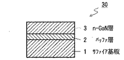
本実施例方法で使用された半導体は、有機金属化合物気相成長法( 以下「M0VPE 」と記す) による気相成長により図2に示す構造に作成された。
【0008】
用いられたガスは、NH3 とキャリアガスH2とトリメチルガリウム(Ga(CH3)3)(以下「TMG 」と記す) とトリメチルアルミニウム(Al(CH3)3)(以下「TMA 」と記す) である。
【0009】
まず、有機洗浄及び熱処理により洗浄したc面を主面とする単結晶のサファイア基板1をM0VPE 装置の反応室に載置されたサセプタに装着する。次に、反応室内の圧力を 5Torrに減圧し、H2を流速 0.3 liter/分で反応室に流しながら温度1100℃でサファイア基板1を気相エッチングした。
【0010】
次に、温度を 800℃まで低下させて、H2を流速3liter/分、NH3 を流速 2liter /分、TMA を 7×10⁻⁶モル/分で供給して1 分間熱処理した。この熱処理によりAlN のバッファ層2が約 500Åの厚さに形成された。次に、1分経過した時にTMA の供給を停止して、サファイア基板1の温度を1150℃に保持し、H2を 2.5liter /分、NH3 を 1.5liter /分、TMG を 1.7×10⁻⁵モル/分で60分間供給し、膜厚約 3μmの n型のGaN 層3を形成した。
【0011】
次に、このようにして形成されたGaN 層3の上面に金属マスク4を図3のように蒸着により形成した試料30を作成し、図1に示す平行平板電極型のプラズマエッチング装置により、露出したGaN 層3をエッチングした。
【0012】
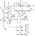
次に、そのエッチング装置について図1を参照して説明する。
図1に示す平行電極型電極装置において、反応室20を形成するステンレス製の真空容器10の側壁には、エッチング用のガスを導入する導入管12が連設されており、その導入管12はガス流速を可変できるマスフローコントローラ14、15、36を介してBCl3ガス、O2がス、Arガスを、それぞれ、貯蔵したボンベ16、17、38に接続されている。そして、BCl3ガス、O2ガス又はArガスがそのボンベ16、17、38からマスフローコントローラ14、15、36を介して反応室20に導入される。又、反応室20はロータリポンプ25、27、拡散ポンプ19、メカニカルブースターポンプ13により排気されており、反応室20の真空度は、バルブ18により調整される。
【0013】
一方、反応室20内には上下方向に対向して、真空容器10から絶縁された電極22と電極24とが配設されている。そして、電極22は接地され、電極24には高周波電力が供給される。その高周波電力は周波数13.56MHzの高周波電源28から整合器26を介して供給される。
【0014】
又、電極24の上には石英板25が載置されており、その石英板29上に、図3図に示す試料30が載置される。
次に、拡散ポンプ19により反応室20内を十分に排気して、反応室20の真空度を 1×10⁻⁵Torr以下にする。その後、Arガスがマスフローコントローラ36により流量8.5cc/分で供給され、コンダクタンスバルブ18により反応室20の真空度は正確に0.06Torrに調整された。そして、電極24と電極22間に0.2 W/cm2 (400W)の高周波電力が供給されて電極間でグロー放電が開始され、導入されたArガスはプラズマ状態となり、試料30,32の表面の前処理としてのエッチング洗浄がが開始された。
【0015】
次に、一旦、電力の供給を停止して、反応室20の真空度が 1×10⁻⁵Torr以下になるまで排気して、BCl3ガスがマスフローコントローラ14により流速7.5 cc/分、Arガスがマスフローコントローラ36により流速21cc/分に制御されて反応室20に導入され、コンダクタンスバルブ18により反応室20の真空度は正確に0.02Torrに調整された。そして、電極24と電極22間に0.2 W/cm2 (400W)の高周波電力が供給されて電極間でグロー放電が開始され、導入されたBCl3とArガスはプラズマ状態となり、試料30,32のエッチングが開始された。
【0016】
160 分間、エッチングを行った結果、試料30は図4に示す構造にエッチングされた。即ち、マスク4で覆われたGaN 層3の部分はエッチングされず、露出したGaN 層3のみが図示する形状にエッチングされた。
【0017】
次に、一旦、電力の供給を停止し、BCl3ガスの供給を停止して、反応室20の真空度が 1×10⁻⁵Torr以下になるまで排気した。その後、Arガスがマスフローコントローラ36により流量8.5cc/分で供給され、コンダクタンスバルブ18により反応室20の真空度は正確に0.06Torrに調整された。そして、電極24と電極22間に0.2 W/cm2 (400W)の高周波電力が供給されて電極間でグロー放電が開始され、導入されたArガスはプラズマ状態となり、試料30,32のエッチングされた表面の後処理としてのエッチング洗浄がが開始された。
【0018】
このようにしてエッチングされた試料30、32をエッチング装置から取り出し、試料30、32の上の金属マスク4を除去した。
その後、その試料に穴径140 μmφ,400μmピッチの穴のあいたステンレス板をマスクとしてアルミニウムを厚さ1.5 μmに蒸着して、図5に示すように電極6を形成した。このようにして形成された電極6の電圧−電流特性(V−I特性)を測定した。その結果を図6に示す。良好なオーミック特性が得られているのが分かる。図から0.25V の時、20mAの電流が流れているのが分かる。このことから、接触抵抗は、12.5Ωであることが分かる。
【0019】
尚、前処理としてのArガスによるエッチング条件としては、Arガスの流量は2cc/分〜500cc/分、RFパワーは100W 〜1kw 、エッチング時間は1 分〜10分の範囲で行うとき、良好なエッチング洗浄が実行される。
【0020】
又、本エッチングの条件としては、BCl3ガスの流量は2cc/分〜200cc/分、Arガスの流量は2cc/分〜500cc/分、RFパワーは100W 〜1kw の範囲で行うとき、エッチング速度が、BCl3ガスだけでエッチングする場合に比べて、2倍に向上した。
【0021】
又、後処理としてのArガスによるエッチング条件としては、前処理と同様に、Arガスの流量は2cc/分〜500cc/分、RFパワーは100W 〜1kw 、エッチング時間は1 分〜10分の範囲で行うとき、良好なエッチング洗浄が実行され、そのエッチングされた表面に金属を蒸着して電極を形成する場合に、良好なオーミック性が得られた。尚、Arガスによる後処理のエッチング洗浄を実行しない場合にはオーミック性は得られなかった。
又、このようにして形成された電極は、従来の炭素、塩素又は/及びフッ素を含むガスでドライエッチグした後、Arでドライエッチングして、その表面に金属を蒸着した場合に比べて、その電極のオーミック特性をより、良好にでき、且つ、接触抵抗を約1/3に低下させることができた。
【0022】
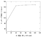
本エッチングにおいて、Ar:BCl3 のガス流量比を1:3,1:2,1:1 として、それぞれの場合において、BCl3ガスの流量を変化させた時のエッチッグ速度を測定した。その結果を図7に示す。BCl3ガスの流量が増加するに連れて、エッチング速度が向上しているのが分かる。又、Arガスの比率が高くなる程、エッチング速度の向上が見られる。又、BCl3ガスの流量を40cc/ 分に固定して、Arガスの流量を0 〜120cc/分で変化させた時のエッチング速度を測定した。その結果を図8に示す。BCl3ガスの流量に対するArガスの流量比を多くするほど、エッチング速度が向上しているのが分かる。しかし、Ar:BCl3 =1:1 で、エッチング速度は飽和する傾向があるが、Arガスが存在しない場合に比べてArガスが存在する場合には、確実に、エッチング速度は向上している。
【0023】
又、本エッチングにおいて、酸素ガスをBCl3ガスに対して、1/100 〜1/10の範囲の割合で混合することで、エッチング速度が、酸素ガスが存在しない場合に比べて、2倍に向上した。
【0024】
上記実施例では、n−GaN について示したが、p−GaN についても、同様にエッチング速度の改善が見られ、エッチングした表面に、NiとAuの2重層による電極を形成したが、オーミック性が改善され、接触抵抗も低下した。さらに、AlX1Ga1−x1N 、InX2Ga1−x2N 、一般式(Al x Ga1−x ) y In1−y N ; (0≦x ≦1,0 ≦y ≦1)の半導体について、上記と同様にエッチングし、電極を形成したが、同様な効果が得られた。
【図面の簡単な説明】
【図1】エッチッグする装置を示した構成図。
【図2】エッチングする試料の構成を示した断面図。
【図3】エッチングする試料の構成を示した断面図。
【図4】エッチングされた試料の形状を示した断面図。
【図5】接触抵抗を測定するために電極の形成された試料の構成を示した断面図。
【図6】エッチングされた面に電極を形成してV−I特性を測定した測定図。
【図7】本エッチングにおいて、BCl3ガスとArガスの流量比率を変化させると共に、BCl3ガスの流量を変化させた時のエッチング速度の測定結果を示す特性図。
【図8】本エッチングにおいて、BCl3ガスに対してArガスの流量比を変化させた時の、Arガスの流量比に対するエッチング速度の測定結果を示す特性図。
【符号の説明】
1…サファイア基板
2…バッファ層
3…GaN 層
4…マスク
5…電極形成部
6…電極
10…真空容器
12,34…導入管
14,15,36…マスフローコントローラ
16,17,38…タンク
19…拡散ポンプ
18…コンダクタンスバルブ
22,24…電極
28…高周波電源[0001]
[Industrial application fields]
The present invention relates to a method for etching a gallium nitride compound semiconductor for improving the dry etching rate of a group III nitride semiconductor, improving ohmic properties, and particularly reducing contact resistance.
[0002]
[Prior art]
Group III nitride semiconductors (eg, AlGaInN) are materials that are attracting attention as blue light emitting diodes. As this semiconductor etching, etching using a plasma gas of BCl 3 has been proposed (Japanese Patent Laid-Open No. 4-34929). Also, as a method of forming an electrode on the surface of the
[0003]
[Problems to be solved by the invention]
However, the above etching method has a low etching rate, and residues are easily deposited on the etched surface, and the method of vapor-depositing metal on the surface etched by the above method improves the ohmic property, but the contact resistance is There is still a problem of being big.
[0004]
Accordingly, an object of the present invention is to improve the etching rate of the
[0005]
[Means for Solving the Problems]
In the invention of
Further, plasma etching of the group III nitride semiconductor with oxygen gas at a flow rate ratio of 1/100 to 1/10 with respect to the gas containing chlorine further activates the gas containing chlorine and contains chlorine. Compared to etching with gas alone, the etching rate could be improved by a factor of about two.
Further, since an inert gas is used after the etching of the group III nitride semiconductor as a post-treatment for plasma etching, adhesion of impurities on the etching surface can be prevented. Therefore, when forming an electrode by vapor-depositing a metal on the surface, the characteristics can be improved.
In the invention of
In the invention of
In the invention of claim 4 , since the surface of the group III nitride semiconductor is cleaned using Ar as an inert gas for pretreatment or posttreatment , adhesion of impurities on the etching surface can be prevented. Therefore, when forming an electrode by vapor-depositing a metal on the surface, the characteristics can be improved.
In the invention of
[0006]
DETAILED DESCRIPTION OF THE INVENTION
Hereinafter, the present invention will be described based on specific examples.
Examples of the group III nitride semiconductor include binary, ternary, and quaternary general formulas (Al x Ga 1-x ) y In 1-y N ; (0 ≦ x ≦ 1, 0 ≦ y ≦ 1) It is a represented semiconductor. First, GaN was etched as follows.
[0007]
The semiconductor used in the method of this example was formed into a structure shown in FIG. 2 by vapor phase growth by an organic metal compound vapor phase growth method (hereinafter referred to as “M0VPE”).
[0008]
The gases used were NH 3 , carrier gas H 2 , trimethylgallium (Ga (CH 3 ) 3 ) (hereinafter referred to as “TMG”) and trimethylaluminum (Al (CH 3 ) 3 ) (hereinafter referred to as “TMA”). )
[0009]
First, a single
[0010]
Next, the temperature was lowered to 800 ° C., and H 2 was supplied at a flow rate of 3 liters / minute, NH 3 was supplied at a flow rate of 2 liters / minute, and TMA was supplied at 7 × 10 −6 mol / minute for heat treatment for 1 minute. By this heat treatment, an
[0011]
Next, a
[0012]
Next, the etching apparatus will be described with reference to FIG.
In the parallel electrode type electrode device shown in FIG. 1, an
[0013]
On the other hand, an
[0014]
A
Next, the inside of the
[0015]
Next, the supply of electric power is once stopped, and the
[0016]
As a result of etching for 160 minutes, the
[0017]
Next, the supply of electric power was stopped once, the supply of BCl 3 gas was stopped, and the
[0018]
The
Thereafter, aluminum was vapor-deposited to a thickness of 1.5 μm using a stainless steel plate with holes having a diameter of 140 μmφ and a pitch of 400 μm as a mask to form an
[0019]
As the etching conditions with Ar gas as pretreatment, the Ar gas flow rate is 2 cc / min to 500 cc / min, the RF power is 100 W to 1 kw, and the etching time is 1 min to 10 min. Etching cleaning is performed.
[0020]
The etching conditions are as follows: the flow rate of BCl 3 gas is 2 cc / min to 200 cc / min, the flow rate of Ar gas is 2 cc / min to 500 cc / min, and the RF power is 100 W to 1 kw. However, it was improved twice as compared with the case of etching only with BCl 3 gas.
[0021]
Etching conditions with Ar gas as post-processing are the same as in the pre-processing, with Ar gas flow rate of 2 cc / min to 500 cc / min, RF power of 100 W to 1 kw, and etching time in the range of 1 min to 10 min. Good etching cleaning was performed, and good ohmic properties were obtained when forming an electrode by depositing metal on the etched surface. It should be noted that ohmic properties were not obtained when post-treatment etching cleaning with Ar gas was not performed.
In addition, the electrode formed in this manner is dry-etched with a gas containing carbon, chlorine or / and fluorine, and then dry-etched with Ar, and a metal is deposited on the surface thereof. The ohmic characteristics of the electrode could be made better and the contact resistance could be reduced to about 1/3.
[0022]
In this etching, the gas flow ratio of Ar: BCl 3 was set to 1: 3, 1: 2, 1: 1, and in each case, the etch rate when the flow rate of BCl 3 gas was changed was measured. The result is shown in FIG. It can be seen that the etching rate increases as the flow rate of BCl 3 gas increases. Moreover, the etching rate is improved as the ratio of Ar gas increases. Further, the etching rate was measured when the flow rate of BCl 3 gas was fixed at 40 cc / min and the flow rate of Ar gas was changed from 0 to 120 cc / min. The result is shown in FIG. It can be seen that the etching rate is improved as the ratio of the Ar gas flow rate to the BCl 3 gas flow rate is increased. However, Ar: BCl 3 = 1: 1 tends to saturate the etching rate, but the etching rate is definitely improved when Ar gas is present compared to when Ar gas is not present. .
[0023]
Also, in this etching, oxygen gas is mixed with BCl 3 gas at a ratio in the range of 1/100 to 1/10, so that the etching rate is doubled compared with the case where oxygen gas is not present. Improved.
[0024]
In the above embodiment, n-GaN was shown, but the improvement of the etching rate was similarly observed for p-GaN, and an electrode with a double layer of Ni and Au was formed on the etched surface. Improved, contact resistance also decreased. Further, Al X1 Ga 1-x1 N, In X2 Ga 1-x2 N, semiconductor of general formula (Al x Ga 1-x ) y In 1-y N ; (0 ≦ x ≦ 1, 0 ≦ y ≦ 1) In the same manner as described above, etching was performed to form an electrode, but the same effect was obtained.
[Brief description of the drawings]
FIG. 1 is a configuration diagram showing an apparatus for etching.
FIG. 2 is a cross-sectional view showing the configuration of a sample to be etched.
FIG. 3 is a cross-sectional view showing a configuration of a sample to be etched.
FIG. 4 is a cross-sectional view showing the shape of an etched sample.
FIG. 5 is a cross-sectional view showing the configuration of a sample on which electrodes are formed in order to measure contact resistance.
FIG. 6 is a measurement diagram in which an VI is formed on an etched surface and VI characteristics are measured.
FIG. 7 is a characteristic diagram showing the measurement result of the etching rate when the flow rate ratio of BCl 3 gas and Ar gas is changed and the flow rate of BCl 3 gas is changed in this etching.
FIG. 8 is a characteristic diagram showing a measurement result of an etching rate with respect to an Ar gas flow ratio when an Ar gas flow ratio is changed with respect to BCl 3 gas in this etching.
[Explanation of symbols]
DESCRIPTION OF
Claims (5)
塩素を含むガスと、不活性ガスと、塩素を含むガスに対して流量比で 1/100 〜 1/10 の割合の酸素ガスとの混合ガスを用いて3族窒化物半導体をプラズマエッチングし、
前記プラズマエッチングの後処理として、3族窒化物半導体のエッチング後に、不活性ガスを用いて、前記3族窒化物半導体の表面を洗浄し、
前記プラズマエッチングされた3族窒化物半導体の表面に金属を蒸着して電極を形成することを特徴とする3族窒化物半導体の電極形成方法。In the method for forming a group 3 nitride semiconductor electrode ,
Plasma etching of a group III nitride semiconductor using a mixed gas of a gas containing chlorine , an inert gas, and an oxygen gas having a flow rate ratio of 1/100 to 1/10 of the gas containing chlorine ,
As a post-treatment of the plasma etching, after etching the group III nitride semiconductor, the surface of the group III nitride semiconductor is cleaned using an inert gas,
3. A method of forming a group III nitride semiconductor electrode, comprising depositing a metal on the surface of the plasma- etched group III nitride semiconductor to form an electrode.
Priority Applications (1)
| Application Number | Priority Date | Filing Date | Title |
|---|---|---|---|
| JP20313096A JP3610397B2 (en) | 1996-07-11 | 1996-07-11 | Method for forming electrode of group 3 nitride semiconductor |
Applications Claiming Priority (1)
| Application Number | Priority Date | Filing Date | Title |
|---|---|---|---|
| JP20313096A JP3610397B2 (en) | 1996-07-11 | 1996-07-11 | Method for forming electrode of group 3 nitride semiconductor |
Publications (2)
| Publication Number | Publication Date |
|---|---|
| JPH1027783A JPH1027783A (en) | 1998-01-27 |
| JP3610397B2 true JP3610397B2 (en) | 2005-01-12 |
Family
ID=16468916
Family Applications (1)
| Application Number | Title | Priority Date | Filing Date |
|---|---|---|---|
| JP20313096A Expired - Fee Related JP3610397B2 (en) | 1996-07-11 | 1996-07-11 | Method for forming electrode of group 3 nitride semiconductor |
Country Status (1)
| Country | Link |
|---|---|
| JP (1) | JP3610397B2 (en) |
Families Citing this family (4)
| Publication number | Priority date | Publication date | Assignee | Title |
|---|---|---|---|---|
| JP2002261326A (en) * | 2001-03-02 | 2002-09-13 | Nagoya Kogyo Univ | Method of manufacturing gallium nitride based compound semiconductor device |
| US8941145B2 (en) * | 2013-06-17 | 2015-01-27 | The Boeing Company | Systems and methods for dry etching a photodetector array |
| JP6151135B2 (en) | 2013-09-03 | 2017-06-21 | 株式会社東芝 | Semiconductor device and manufacturing method thereof |
| JP6530356B2 (en) * | 2016-09-01 | 2019-06-12 | 大陽日酸株式会社 | Method of cleaning nitride semiconductor manufacturing apparatus |
-
1996
- 1996-07-11 JP JP20313096A patent/JP3610397B2/en not_active Expired - Fee Related
Also Published As
| Publication number | Publication date |
|---|---|
| JPH1027783A (en) | 1998-01-27 |
Similar Documents
| Publication | Publication Date | Title |
|---|---|---|
| US5205905A (en) | Dry etching method for semiconductor | |
| US9466479B2 (en) | System and process for high-density, low-energy plasma enhanced vapor phase epitaxy | |
| Rudder et al. | Remote plasma‐enhanced chemical‐vapor deposition of epitaxial Ge films | |
| US4946548A (en) | Dry etching method for semiconductor | |
| JPH07297446A (en) | Group III nitride semiconductor light emitting device | |
| US5811319A (en) | Methods of forming electrodes on gallium nitride group compound semiconductors | |
| JP3610397B2 (en) | Method for forming electrode of group 3 nitride semiconductor | |
| JP2623463B2 (en) | Gallium nitride based compound semiconductor electrode forming method | |
| CN115692570B (en) | An LED chip based on an aluminum oxide silicon oxide composite substrate and a manufacturing method thereof | |
| JP2654454B2 (en) | Dry etching method for semiconductor | |
| JP3490103B2 (en) | Gallium nitride based compound semiconductor light emitting device and method of manufacturing the same | |
| JP2706660B2 (en) | Gallium nitride based compound semiconductor electrode forming method | |
| JPH08125222A (en) | Method for manufacture of group iii nitride semiconductor | |
| JP2654455B2 (en) | Dry etching method for semiconductor | |
| JP2740818B2 (en) | Surface processing method of gallium nitride based compound semiconductor | |
| Han et al. | Nonselective etching of GaN/AlGaN heterostructures by Cl2/Ar/BCl3 inductively coupled plasmas | |
| JP3002205B2 (en) | Surface processing method of gallium nitride based compound semiconductor | |
| JP3639144B2 (en) | Semiconductor dry etching method | |
| JPH07302770A (en) | Method for manufacturing electrode for 3-5 group compound semiconductor | |
| US20240234126A1 (en) | Method for preparing a microelectronic component comprising a layer with a basis of a iii-v material | |
| JPH07263749A (en) | Manufacture of iii group nitride semiconductor | |
| JPH11103134A (en) | Method for manufacturing semiconductor device | |
| JPH07288321A (en) | Electrode material for 3-5 group compound semiconductor and its electrode | |
| CN101591773A (en) | Vapor Deposition System | |
| CN120770064A (en) | Method for forming gallium nitride film |
Legal Events
| Date | Code | Title | Description |
|---|---|---|---|
| A521 | Written amendment |
Free format text: JAPANESE INTERMEDIATE CODE: A523 Effective date: 20040901 |
|
| A61 | First payment of annual fees (during grant procedure) |
Free format text: JAPANESE INTERMEDIATE CODE: A61 Effective date: 20040930 |
|
| R150 | Certificate of patent (=grant) or registration of utility model |
Free format text: JAPANESE INTERMEDIATE CODE: R150 |
|
| FPAY | Renewal fee payment (prs date is renewal date of database) |
Free format text: PAYMENT UNTIL: 20081029 Year of fee payment: 4 |
|
| FPAY | Renewal fee payment (prs date is renewal date of database) |
Free format text: PAYMENT UNTIL: 20081029 Year of fee payment: 4 |
|
| FPAY | Renewal fee payment (prs date is renewal date of database) |
Free format text: PAYMENT UNTIL: 20091029 Year of fee payment: 5 |
|
| FPAY | Renewal fee payment (prs date is renewal date of database) |
Free format text: PAYMENT UNTIL: 20091029 Year of fee payment: 5 |
|
| FPAY | Renewal fee payment (prs date is renewal date of database) |
Free format text: PAYMENT UNTIL: 20101029 Year of fee payment: 6 |
|
| FPAY | Renewal fee payment (prs date is renewal date of database) |
Free format text: PAYMENT UNTIL: 20101029 Year of fee payment: 6 |
|
| FPAY | Renewal fee payment (prs date is renewal date of database) |
Free format text: PAYMENT UNTIL: 20111029 Year of fee payment: 7 |
|
| FPAY | Renewal fee payment (prs date is renewal date of database) |
Free format text: PAYMENT UNTIL: 20111029 Year of fee payment: 7 |
|
| FPAY | Renewal fee payment (prs date is renewal date of database) |
Free format text: PAYMENT UNTIL: 20121029 Year of fee payment: 8 |
|
| FPAY | Renewal fee payment (prs date is renewal date of database) |
Free format text: PAYMENT UNTIL: 20121029 Year of fee payment: 8 |
|
| FPAY | Renewal fee payment (prs date is renewal date of database) |
Free format text: PAYMENT UNTIL: 20131029 Year of fee payment: 9 |
|
| LAPS | Cancellation because of no payment of annual fees |