JP3607032B2 - Nonvolatile ferroelectric memory and driving method thereof - Google Patents
Nonvolatile ferroelectric memory and driving method thereof Download PDFInfo
- Publication number
- JP3607032B2 JP3607032B2 JP05498997A JP5498997A JP3607032B2 JP 3607032 B2 JP3607032 B2 JP 3607032B2 JP 05498997 A JP05498997 A JP 05498997A JP 5498997 A JP5498997 A JP 5498997A JP 3607032 B2 JP3607032 B2 JP 3607032B2
- Authority
- JP
- Japan
- Prior art keywords
- plate
- plate line
- circuit
- selection circuit
- line selection
- Prior art date
- Legal status (The legal status is an assumption and is not a legal conclusion. Google has not performed a legal analysis and makes no representation as to the accuracy of the status listed.)
- Expired - Fee Related
Links
Images


Classifications
-
- G—PHYSICS
- G11—INFORMATION STORAGE
- G11C—STATIC STORES
- G11C11/00—Digital stores characterised by the use of particular electric or magnetic storage elements; Storage elements therefor
- G11C11/21—Digital stores characterised by the use of particular electric or magnetic storage elements; Storage elements therefor using electric elements
- G11C11/22—Digital stores characterised by the use of particular electric or magnetic storage elements; Storage elements therefor using electric elements using ferroelectric elements
Landscapes
- Engineering & Computer Science (AREA)
- Computer Hardware Design (AREA)
- Semiconductor Memories (AREA)
- Dram (AREA)
- Semiconductor Integrated Circuits (AREA)
- Non-Volatile Memory (AREA)
Description
【0001】
【発明の属する技術分野】
本発明は、RFIDシステムに用いられるトランスポンダに係り、とくに、トランスポンダに搭載され、情報記憶用キャパシタに強誘電体膜を用いたメモリセルのアレイを有する不揮発性強誘電体メモリ及びその駆動方法及びIDカードに関するものである。
【0002】
【従来の技術】
RFID(Radio Frequency Identification)システムは、電波を用いた非接触型タグ・システム(識別器)のことであり、パソコン、コントローラ、アンテナ等で構成されるホスト側とトランスポンダとから構成されている。トランスポンダは、不揮発性強誘電体メモリなどのチップを搭載している。
強誘電体メモリセルを用いた不揮発性強誘電体メモリは、低消費電力の半導体記憶装置として近年盛んに研究開発がなされている。この不揮発性強誘電体メモリは、米国特許4,873,664(Eaton, Jr.) やS.S. Eaton, Jr. et al.“A Ferroelectric DRAM Cell for High Density NVRAMs ”, ISSCC Digest of Technical Papers, pp. 130−131, Feb. 1988等に記載されている。
強誘電体メモリセルの情報記憶用キャパシタには、チタン酸バリウム(BaTiO3 )、チタン酸ジルコン酸鉛(Pb(Zr,Ti)O3 ;PZT)、ランタンドープドチタン酸ジルコン酸鉛((Pb,La)(Zr,Ti)O3 ;PLZT)、ニオブ酸リチウム(LiNbO3 )、ニオブ酸カリウムリチウム(K3 Li2 Nb5 O15)などから構成された強誘電体膜が用いられている。これらの強誘電体膜は、電圧を印加することによって分極が生じる。そして電圧と分極との関係は、いわゆるヒステリシス特性を呈する。
【0003】
この関係について、発明者が上記強誘電体膜の特性を測定したところ、外部から印加される物理的ストレスが上述のヒステリシス特性に影響を与えることが分かった。すなわち、成膜後に物理的なストレスを強誘電体膜に印加するとヒステリシスループが小さくなり、分極の保持特性が劣化することが分かった。強誘電体メモリは、分極をデータの保持に用いている。従って、外部から印加される物理的ストレスはデータの保持特性の劣化につながることは明らかである。
図45(a)に従来の不揮発性半導体記憶装置のメモリセルアレイと周辺回路の配置を示す。複数のメモリセルアレイが並列して配置され、ロウデコーダ(RD)(ワード線選択回路)40は、これらに共用されている。複数のワード線WLは、外部から入力されたアドレス信号に応じてロウデコーダ回路40によって選択される。プレート線PLは、ワード線WLと同じ様にメモリセルアレイ共通に接続され(セルキャパシタの対向電極に接続)、プレートデコーダ(PD)(プレート線選択回路)38によって駆動される。プレートデコーダ38は、NAND回路とインバータ回路を直列に接続してなり、ワード線信号とプレート線制御信号との論理をとってプレート電極を制御する。書き込みや読み出しなどのワード線信号やプレート線信号は、パルス信号であるが、図45(b)に示すようにプレート線を制御するプレート線信号の方がワード線信号よりパルス幅は短い。このようにプレート線信号が短時間で立ち上げ立ち下げを行うのでメモリセルの情報の読み出し速度は、プレート線信号のパルスに律速されてしまう。もしこれを回避するためにはプレート線選択回路のインバータ回路のトランジスタを大きくする必要がある。しかし、インバータ回路のトランジスタを不必要に大きくするとロウデコーダ回路のワード線駆動部のピッチとプレート線選択回路のピッチが合わなくなり、ワード線とプレート線の間隔は、広い方に律速されるので、その分面積の無駄が大きくなる。
【0004】
【発明が解決しようとする課題】
前述のように従来のトランスポンダに用いられる不揮発性強誘電体メモリは、プレート線をデコード(パルス駆動)する場合において、そのCR(容量・抵抗)が大きいので、プレート線が遅延して動作するためセルに書かれているデータを十分に読み出すことができない、またはセルにデータを十分に書き込むことができない恐れがある。また、ワード線は、メモリセルのトランジスタのゲートに接続されるのみであるのに対して、プレート線は、前述のようにセルキャパシタの対向電極に共通接続され、そのため付加容量が非常に大きい。その結果、ワード線が駆動される場合に比べて、プレート線が駆動されるには時間が掛かる。プレート線信号が短時間で立ち上げ立ち下げを行うのでメモリセルの情報の読み出し速度は、プレート線信号のパルスに律速されてしまうのでプレート線の信号速度を高めることは必要なことである。
また、とくにメモリカード等に不揮発性強誘電体メモリを搭載した場合、メモリカードの厚さが薄いと外部から容易に物理的ストレスが加わり、その結果データ保持特性が劣化するという問題があった。
【0005】
ところがこのヒステリシス特性は、温度によってその形状が大幅に変化することが知られている。すなわち、高温(例えば80℃)でのヒステリシスループは低温(例えば室温である25℃)のものと比較してループが小さくなり、分極の保持特性が劣化する。強誘電体メモリは分極をデータの保持に用いている。従って、チップ内の熱源の存在は、データの保持特性の劣化につながる。
特に無電源型メモリカード等に不揮発性強誘電体メモリを搭載した場合、電源供給回路や整流回路等で発生する熱は、強誘電体メモリのデータ保持特性に影響を与えることがある。
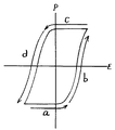
図46は、強誘電体膜をキャパシタに用いたメモリセル(FRAMセル)に用いる強誘電体材料のヒステリシスカーブである。書き込み、読み出し動作を行う際には、a→b→c→dの順にカーブの縁辺を沿うように状態を変化させる。しかし、実際に電流が流れるのはb,dのところである。セルの分極を反転させるのに必要な電流は、わずかb,dのところだけしか流れない。したがって、図47(a)のようにプレート線PLを駆動した場合でもプレート線PLの立上がりの前半では電流は殆ど流れないのに対し、後半ではパルス的に電流が流れる(図47(b))。このように極めて短時間の間に集中的に電流が流れると最大電流量は大きくなり、この結果電源電位の変動やこれにより引き起こされる基準電位の変動による各種の誤動作が生ずる可能性がある。
【0006】
本発明は、上記の事情に鑑みてなされたものであり、プレート線をデコード (パルス駆動)する際に誤動作を引き起こす恐れを防止してその駆動速度を向上させた構造を有するプレート線を備え、トランスポンダに搭載される不揮発性強誘電体メモリを提供する。
また、本発明は、プレート線の駆動速度を向上させながらプレート線に流れる駆動電流の最大電流量を小さくすることができる不揮発性強誘電体メモリ及びその駆動方法を提供する。
【0007】
【課題を解決するための手段】
本発明の不揮発性強誘電体メモリは、電極間絶縁膜に強誘電体を用いた情報記憶用のキャパシタと電荷転送用のMOSトランジスタとが直列に接続されてなるメモリセルが行列状に配置されたメモリセルアレイと、それぞれ同一のメモリセルのMOSトランジスタのゲートに共通に接続された複数本のワード線と、それぞれ同一のメモリセルのキャパシタの一端に共通に接続された複数本のプレート線と、上記ワード線と上記プレート線が並行に配列されプレート線が対応するワード線に対してさらに複数のプレート線が分割されることと、それぞれ同一のメモリセルのMOSトランジスタの一端に共通に接続された複数本のビット線と、アドレス信号に基づいて上記複数本のワード線のうちの一部を選択するワード線選択回路と、上記複数本のワード線と、例えば、チップイネーブル(Chip Enable)信号( /CE)などの外部端子によって生成された信号とで形成されるプレート線選択回路と、そのプレート線選択回路がそれぞれのワード線に対して複数存在していることを特徴とする。また、ワード線に対応する複数のプレート選択回路は、アドレス信号によってそれぞれ独立して動作し、通常動作時にすべてのプレート選択回路が動作することがないことを特徴としている。
複数のワード線のそれぞれのワード線に対して、それぞれ複数のプレート線選択回路(プレートデコーダ)を持ち、分割されたプレート線を有し、それぞれを部分デコードするのは、例えば、カラムアドレス信号などのアドレス信号によって行われるので、CRが大きいプレート線でなくなり、動作マージンを十分持ち誤動作する恐れが少なくなる。
【0008】
また、本発明は、強誘電体膜をキャパシタに用いた不揮発性強誘電体メモリのプレート線を行方向に複数に分割し、これを駆動した構成において、分割したプレート線の駆動タイミングをずらすことにより一時的に流れる電流を減少させることを特徴としている。
また、本発明の不揮発性強誘電体メモリは、強誘電体膜を情報記憶キャパシタとして用いる強誘電体メモリセルをマトリックス状に配置してなるメモリセルアレイと、同一行のメモリセルのトランジスタのゲートを共通接続してなるワード線と、同一行のメモリセルのキャパシタの対向電極を共通接続してなるプレート線と、前記ワード線を選択し駆動するロウデコーダとを備え、前記プレート線が行方向にn分割され、n個のプレート線選択回路がその一端にそれぞれ接続され、前記メモリセルのトランジスタのゲート容量は前記メモリセルのキャパシタ容量より小さいことを特徴とする。
【0011】
【発明の実施の形態】
以下、図面を参照して発明の実施の形態を説明する。
RFIDシステムは、電波を用いた非接触型タグ・システム(識別器)のことで、一般的には非接触データ・キャリア・システムともいう。本発明は、このシステムに用いるトランスポンダ及びこのトランスポンダに搭載する不揮発性強誘電体メモリ及びその駆動方法に関するものである。
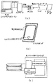
図43は、本発明のトランスポンダを用いるRFIDシステム全体のシステム構成図である。RFIDシステムは、パソコン、コントローラ、アンテナ等で構成されるホスト側と、トランスポンダと呼ばれるデータ・キャリアで構成される(図43(a))。トランスポンダは、カード基板にFRAMとASICが1チップ化されたモノリシックRFIDチップ及び電力受信、データ受信/送信を兼ねるアンテナを内蔵するシンプルな構成である(図43(b))。図43(c)は、モノリシックRFIDチップの平面図である。ホスト側からは必要に応じてコマンド及びデータを搬送波に乗せて送信するが、トランスポンダ側ではその搬送波により必要な電力を発生させ、データの書き込み及び読み出しと送信に利用してホスト側に情報を返す。非接触タグは、電池が不要であり、FRAMの記憶内容を電波を使って非接触で読み取り、その内容を書き換えることにより人の入退出などの管理に活用することが可能である。例えば、服のポケットに定期券用の非接触タグを入れたまま改札したり、非接触タグを自動車につけて走り高速道路の料金所でいちいち精算するために止まらなくて済むようしたり、人の介在なしに駐車場の出入りを監視・管理するなどの用途に利用することが可能である。また、回遊魚や家畜の行動を管理することなどにも利用できる。
【0012】
図44は、トランスポンダの内部回路の詳細を示す。外部から入力される電磁場を検知するLC回路と、LC回路が検出した電磁場から信号を生成する回路(FSK復調回路)58と、LC回路が検出した電磁場から電源電圧を発生させる回路(整流ブリッジ)59と、電源電圧の立ち上がりを検出してパワーオン信号を出力するパワーオン回路60と、強誘電体膜を電極間に有する強誘電体キャパシタと電荷転送用のMOSトランジスタとからなるメモリセルを複数個行列状に配置し、例えば、同一行に属するメモリセルのMOSトランジスタを同一のワード線でそれぞれ共通接続し、同一行に属するメモリセルの強誘電体キャパシタの一方の電極を同一のキャパシタプレート線でそれぞれ共通接続し、同一列に属するメモリセルのMOSトランジスタの一方の端子を同一のビット線でそれぞれ共通接続して構成したFRAMセルアレイ31等から構成されている。
【0013】
次に、図1乃至図15を参照して第1の実施例を説明する。
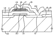
図1にトランスポンダに搭載される不揮発性強誘電体メモリの断面図を示す。この強誘電体メモリは、図43にはモノリシックRFIDチップとして示されているようにトランスポンダに搭載されて使用される。P型シリコン基板10の表面にシリコン酸化膜からなる素子分離絶縁膜13が形成され、この素子分離絶縁膜13に区画された領域にMOSトランジスタが形成される。MOSトランジスタは、N型拡散領域からなるソース/ドレイン領域11、12、ゲート絶縁膜21、ポリシリコンからなるゲート電極20等から構成される。ゲート電極20は、ワード線(WL)と称される。このMOSトランジスタ上には酸化シリコン(SiO2 )などの層間絶縁膜14が形成され、この層間絶縁膜14にはソース領域12に至るコンタクトホール22が形成されている。層間絶縁膜14上には強誘電体キャパシタが形成されている。強誘電体キャパシタは、下層電極15、PZT膜などからなる強誘電体膜16、上層電極17から構成される。下層電極15は、プレート電極(プレート線)(PL)と称される。この強誘電体キャパシタは、シリコン酸化膜などからなる層間絶縁膜18に覆われ、強誘電体キャパシタの上層電極17とソース領域12とは層間絶縁膜18のコンタクトホール及び層間絶縁膜14のコンタクトホール22を介してアルミニウムなどの接続配線19により電気的に接続されている。
【0014】
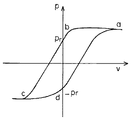
図2にPZT膜等の強誘電体薄膜の印加電圧/分極特性を示す。強誘電体薄膜は図2に示すようにヒステリシス特性を有する。そして、電圧を印加しない状態すなわちV=0(V)の状態での残留分極Prが「正」であるか「負」であるかによって、データを記憶することができる。
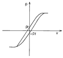
図3は、不揮発性強誘電体メモリの強誘電体メモリセルとしては好ましくないヒステリシス特性である。すなわち、残留分極Prが非常に小さく、その結果、センスアンプによる読み出しマージンが低下する、外部からの撹乱により容易にデータが消失してしまう等の問題が存在する。図3に示す特性は、80℃の高温状態でのヒステリシス特性である。
続いて、図4、図5を用いて強誘電体薄膜を用いたメモリセルの書き込み動作を説明する。FRAMセルを用いた不揮発性強誘電体メモリは、2つのMOSトランジスタQ1、Q2と強誘電体キャパシタC1、C2により一つのメモリセルを構成する。そして、図4(a)の状態、すなわちキャパシタC1には図中上向きの矢印に示すように上方向の分極(以下、正分極と称する)が、キャパシタC2には図中下向きの矢印に示すように下方向の分極(以下、負分極と称する)が現れている状態を“1”と定義し、図4(b)の状態、即ちキャパシタC1には負分極が、キャパシタC2には正分極が現れている状態を“0”と定義する。
【0015】
(“1”書き込み動作)
以下、メモリセルに“1”を書き込む場合のステップを示す。
まず、ビット線BLに5Vを印加し、ビット線 /BL(「 /」は反転信号を表わす、以下、同じ)には0Vを印加する。そしてワード線WLには7Vを印加し、プレート電極PLには0Vを印加する。この状態は、キャパシタC1が図2のaの状態であり、キャパシタC2が図2のbの状態にある。
続いて、PLを5Vにする。この結果、キャパシタC1は、図2のbの状態になり、キャパシタC2は図2のcの状態になる。
続いて、PLを0Vにする。この結果、キャパシタC1は、図2のaの状態になり、キャパシタC2は図2のdの状態になる。
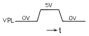
図5に書き込み時のプレート電極PLの電位(VPL)の変化を示す。
以上のようにして、図4(a)の状態、すなわちキャパシタC1には正分極が現れ、キャパシタC2には負分極が現れて“1”書き込みが実現される。
【0016】
(“0”書き込み動作)
以下、メモリセルに“0”を書き込む場合のステップを示す。
まず、ビット線BLに0Vを印加し、ビット線 /BLには5Vを印加する。そしてワード線WLには7Vを印加し、プレート電極PLには0Vを印加する。この状態では、キャパシタC1が図2のbの状態にあり、キャパシタC2が図2のaの状態にある。
続いて、PLを5Vにする。この結果、キャパシタC1は、図2のcの状態になり、キャパシタC2は、図2のbの状態になる。
続いて、PLを0Vにする。この結果、キャパシタC1は、図2のdの状態に、なり、キャパシタC2は図2のaの状態になる。
以上のようにして、図4(b)の状態、すなわちキャパシタC1には負分極が現れ、キャパシタC2には正分極が現れて“0”書き込みが実現される。
【0017】
以上のような不揮発性強誘電体メモリは、消費電力が僅少のため、無電源ID装置等に用いられる。無電源ID装置とは、外部から電波を受信し、この電波を整流して得られた直流電圧を電源として用いると共に、この電波搬送信号とされた情報を受信・検波して外部とデータの入出力を行う。無電源ID装置には電波の送信回路も搭載されるのが通常である。以上のように構成すると、IDカードを無電源で構成でき、外部との情報のやりとりも親機と全く無接触で行うことが可能となる。以上のような無電源IDカードは、免許証、商品タグ、身分証明書、定期券、スキー場のリフト券等に応用が期待されている。
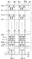
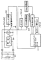
続いて、図6及び図7に不揮発性強誘電体メモリのメモリセルアレイと周辺回路との配置を示す。メモリセルアレイ31〜34は、並列して配置され、ワード線選択回路(ロウデコーダRD)40は、これらに共用されている。大きく複数のメモリセルアレイ31〜34を2分割したときに、中央部にロウデコーダ40が配置され、これに複数のワード線WLが配線されている。そして、左右に分かれて配置されているメモリセルアレイをさらに分割してプレート線選択回路(プレートデコーダPD)35、36がそれぞれ配置され、このプレートデコーダ35、36からそれぞれプレート線PL(PL1、PL2、PL3、PL4)が配線されている。
【0018】
ワード線WLは、外部から入力されたアドレス信号に応じてロウデコーダ40によって選択される。プレート線PLは、各メモリセルアレイ毎に分割して設けられており、プレートデコーダ35、36によって図5のように駆動される。まず、センスアンプ回路(S/A)41〜44は、各メモリセルアレイ毎に設けられており、読み出し時にビット線に現れた微小電位差を増幅する。カラムゲート回路(図示しない)は、カラム選択線に基づきデータ線とビット線とを選択的に接続する。カラムデコーダ(CD)56は、外部から入力されたアドレス信号に応じてカラム選択線(図示しない)を選択する。データ線センスアンプ回路(図示しない)は、データ線上のデータを増幅する。
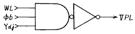
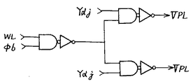
図8に示す回路は、本発明のプレートデコーダである。プレートデコーダは、NAND回路とこのNAND回路の出力信号が入力されるインバータ回路とから構成され、インバータ回路は、プレート電圧(VPL)として電源電圧(Vcc)を供給する。NAND回路の入力信号として、まずφ6信号は、 /CE(Chip Enable信号) (DRAMならば /RAS)からの遅延信号及びパルスを持った信号である(図9参照)。Yα信号は、一部のアドレス信号で横方向に関わるアドレスである。さらに、WLは、それぞれに対応するワード線を示している。ここで、例えば、図6及び図7に示すメモリセルアレイでは、1本のワード線WLに対して4本の分割されたプレート線PLが存在している。そこで、このアドレス信号(Yα)によって4本のプレート線から1本が選択されることとなる。これによって今までのプレート線より少なくとも1/4の容量となるため、プレート線のデコードが高速になり誤動作を防ぐことができる。
【0019】
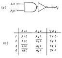
図11は、プレートデコーダの他の実施例である。例えば、アドレスi、jという2つが有ると、アドレスバッファによってAic/ /Aic、Ajc/ /Ajcという相補的な信号が生成される(図10参照)。これを使ってプレコーダ(Precoder)を作ると図12(a)に示すようになる。図12(b)に示す4種類の入力方法がある。この方法により4つのYα信号(Yα0、Yα1、Yα2、Yα3)が生成される。この4つのYαj信号を図11のプレートデコーダに入力すると、4つのプレート電圧(VPL)の内1つのVPLがパルス駆動することができる。図8及び図11のプレートデコーダの入力信号(WL、VPL、 /CE(φ6)は、図13のタイミング図に示すような電圧波形を有している。
図6及び図7に示すロウデコーダの詳細な回路図を図14に示す。ロウデコーダは、ワード線の選択を行う回路である。行アドレスをプリデコードした信号Xαj、Xαk、Xαlにより1組のデコーダが選択される。1組のデコーダには4本のワード線が接続され、信号WDRVi〜WDRVlによってこの内1本が選択される。
【0020】
また、図6及び図7のメモリセルアレイに用いられるセンスアンプの詳細を図15に示す。図15に、メモリセルアレイ31、センスアンプ回路41、カラムゲート回路51の詳細が示されている。メモリセルアレイ31は、行列状に配置されたメモリセル30を含み、同一列に配置されたメモリセルは、同一ビット線対(BLn; /BLn)(n=1、2、・・・)に接続され、同一行に配置されたメモリセルは、同一ワード線WLn(n=1、2、・・・)、プレート線PLn(n=1、2、・・・)に接続される。センスアンプ回路41は、複数のセンスアンプ411から構成され、単独のセンスアンプは、交差接続されたP型の二つのMOSトランジスタと、交差接続されたN型の二つのMOSトランジスタとから構成される。このセンスアンプ411は、P型センスアンプ駆動線SAP及びN型センスアンプ駆動線 /SANによって駆動制御される。また、ビット対毎に2つのN型MOSトランジスタからなるイコライズ回路412が接続され、イコライズ選択線EQにより制御される。カラムゲート回路51は、ビット線毎に接続されたカラムゲートから構成され各カラムゲートは、2つのMOSトランジスタから構成される。これらのMOSトランジスタは、カラム選択線CSLによって選択駆動される。
【0021】
次に、図16乃至図18を参照して第2の実施例を説明する。
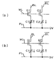
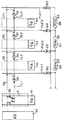
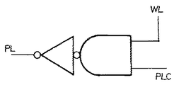
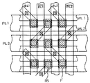
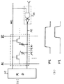
図16は、トランスポンダに搭載される不揮発性強誘電体メモリ(FRAM)のメモリセルアレイと周辺回路の詳細な構造を示す部分回路図である。強誘電体膜を情報記憶キャパシタとして用いるメモリセル(FRAMセル)30をマトリックス状に配置してなるメモリセルアレイ31〜34が配置されている。ワード線WLは、それらメモリセル30のポリシリコンゲートを共通接続している。同一行のメモリセル30のキャパシタの対向電極を共通接続してなるプレート線PL1〜PL4は、行方向にn分割(ここでは4分割)され、4個のプレート線選択回路35〜38がその一端にそれぞれ接続されている。これらプレート線選択回路は、NAND回路とインバータ回路とから構成され、インバータ回路は、プレ−ト線に電源電圧Vccをプレート電圧(VPL)として供給する。プレート線選択回路に沿って列方向に複数のプレート線制御線PLC1〜PLC4が配列されている。プレート線制御線には、これらプレート線制御線を独立に駆動するプレート線制御線駆動回路62〜65がそれぞれ接続さている。プレート線選択回路のNAND回路の2入力の一方にプレート線制御線PLCが接続され、他方にゲート線WLが接続されている。
【0022】
この実施例の特徴は、図16に示すように、メモリセルアレイを複数に分割し、プレート線を分割駆動した構成において、プレート線の駆動タイミングをずらすことにより一時的に流れる最大電流を減らすことにある。図に示すように、例えば、4つのブロックにそれぞれ独立に駆動制御されるプレート線PL(PL1〜PL4)が配置されており、これらのプレート線PLの駆動を制御するプレート線制御線駆動回路63〜65は、その入力にそれぞれ遅延線チェイン(D1、D2、D3)66〜68を有している。これにより図17(a)に示すように各プレート線PL(PL1〜PL4)の立上がりの後半が若干ずつずれるので、電流は分散して流れる。その結果、最大電流量( |Isum |)は、従来(図17(b))に比較して著しく低下するようになる。
この実施例において、遅延線の遅延時間の調整は重要である。遅延時間が長ければ、読み出しや書き込みサイクルが長くなり、高速メモリの提供は、不可能になる。前述のようにFRAMにおいてはプレート線の立上がり若しくは立ち下がりの後半のみにパルス的に電流が流れるに過ぎない。したがって各プレート線の立上がりもしくは立ち下がり時間は、オーバーラップしても構わない。具体的に述べると、各プレート線の立上がりに5nsかかるとする。しかし実際に電流が流れるのは、最後の0.5nsの部分である。したがってこの場合は、4.5ns分はオーバーラップさせても良い。したがって、遅延線の遅延時間は0.5ns以上と決定される。より一般的にプレート線の立上がり時間をtとし、ランプ状態に立上がるとすると、ほぼ9割の時間では電流は流れず、残りの1割で多くの電流が流れることが知られている。この結果、1/10以上の遅延時間を設定すれば良い。遅延線の例を図18に示す。遅延線は、一般にインバータ回路を直列接続して構成するが、遅延時間が1nsよりも小さい場合は、金属配線のみで足りる場合も考えられる。図18(a)、(b)は、インバータ回路、図18(c)は、アルミニウムなどの金属配線の例を示している。
【0023】
次に、図19乃至図23を参照して第3の実施例を説明する。
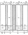
図19は、トランスポンダに搭載される不揮発性強誘電体メモリのメモリセルアレイと周辺回路の詳細な構造を示す部分回路図である。強誘電体膜を情報記憶キャパシタとして用いるメモリセル(FRAMセル)30をマトリックス状(行列状)に配置してなるメモリセルアレイ31、32・・・が配置されている。ワード線WLは、それらメモリセル30のポリシリコンゲートを共通接続している。ワード線WLが形成されている半導体基板の上に層間絶縁膜を介してアルミニウムなどの金属配線ワード線Al−WLが形成されている。このワード線WLは、金属配線ワード線Al−WLに所定間隔毎にシャント線SLにより接続されている。同一行のメモリセル30のキャパシタの対向電極を共通接続してなるプレート線PL(PL1、PL2、・・・)は、行方向にn分割され、n個のプレート線選択回路35、36がその一端にそれぞれ接続されている。プレート線選択回路35、36は、NAND回路とインバータ回路とから構成され、インバータ回路は、プレ−ト線に電源電圧を供給する。プレート線選択回路35、36は、このシャントされる領域に配置されており、メモリセルアレイ間に配置されている。プレート線選択回路に沿って列方向に複数のプレート線制御線PLC(PLC1、PLC2・・・)が配列されている。プレート線制御線PLCには、これらプレート線制御線PLCを独立に駆動するプレート線制御線駆動回路61、62・・・がそれぞれ接続さている。
【0024】
プレート線選択回路のNAND回路の2入力の一方にプレート線制御線が接続され、他方にゲート線が接続されている。
メモリセルのトランジスタのゲート容量(C1)は、前記メモリセルのキャパシタ容量(C2)より小さい(C1<C2)。
図20は、プレート線選択回路35、36の回路図である。プレート線PL(PL1、PL2・・・)は、このプレート線選択回路35、36によって駆動される。プレート線選択回路35、36は、NAND回路とインバータ回路とを直列に接続してなり、ワード線信号WLとプレート線制御信号PCLとの論理をとってプレート電極を制御する。
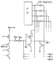
図21は、図20の詳細な回路図であり、インバータ回路は、NチャネルトランジスタN2とPチャネルトランジスタP2とから構成されている。この実施例では、電源電圧Vccは、5Vである。
図22は、図19に示すロウデコーダ(RD)40の詳細な回路図である。図22に示すようにロウデコーダ40内のトランジスタのゲートの幅/長さ比((W/L)1 )とメモリセル30のトランジスタのゲート容量(C1)との積は、プレート線選択回路PL内のトランジスタのゲートの幅/長さ比( (W/L)2 )と前記メモリセルのキャパシタ容量(C2)との積にほぼ等しく((W/L)1 ・C1〜(W/L)2 ・C2)してあるので信号の立上がり時間と立ち下がり時間を等しくすることができる。
【0025】
また、図22に示すように、ロウデコーダは、最終段にPチャネルトランジスタP1とNチャネルトランジスタN1を直接に接続されたインバータ構成をとり、プレート線選択回路35、36は、最終段にPチャネルトランジスタP2とNチャネルトランジスタN2を接続して構成したインバータを有し、ロウデコーダ内のNチャネルトランジスタのゲートの幅/長さ比((W/L)n1)とメモリセルMSのトランジスタのゲート容量(C1)との積は、前記プレート線選択回路内のNチャネルトランジスタN2のゲートの幅/長さ比((W/L)n2)とメモリセルMSのキャパシタ容量(C2)との積にほぼ等しく構成されている((W/L)n1・C1〜(W/L)n2・C2)。またロウデコーダRD内のPチャネルトランジスタP1のゲートの幅/長さ比((W/L)p1)とメモリセルMSのトランジスタのゲート容量(C1)との積は、プレート線選択回路35、36内のPチャネルトランジスタP2のゲートの幅/長さ比((W/L)p2)と前記メモリセルのキャパシタ容量(C2)との積にほぼ等しく構成されている((W/L)p1・C1〜(W/L)p2・C2)。
【0026】
また、ロウデコーダRD内のNチャネルトランジスタN1のゲートの幅/長さ比((W/L)n1)は、ロウデコーダRD内のPチャネルトランジスタP1のゲートの幅/長さ比((W/L)p1)より小さく構成されている((W/L)n1<W/L)p1。さらにプレート線選択回路35、36内のNチャネルトランジスタN2のゲートの幅/長さ比((W/L)n2)は、プレート線選択回路35,36内のPチャネルトランジスタP2のゲートの幅/長さ比((W/L)p2)より小さくなるように構成されている((W/L)n2<(W/L)p2)。
図23に示すように金属配線ワード線Al−WLは、ワード線WLとシャント接続されている。シャント線SLは、一定間隔毎に配置されている。本発明では、所定のシャント線SL毎にこのシャント線SLとプレート線PL1、PL2、・・・の一端に接続されたプレート線選択回路35、36、37、38とが接続されている。この実施例では、プレート線選択回路と直接接続されたシャント線は、3本毎に配置されている。したがって、メモリセルのトランジスタのゲート容量(C1)とメモリセルのキャパシタ容量(C2)との比(C1:C2)は、1:4となりキャパシタ容量(C2)の方が4倍程度大きいことになる。
【0027】
次に、図24乃至図28を参照して第4の実施例を説明する。
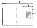
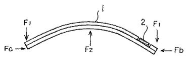
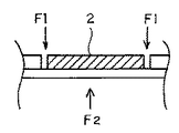
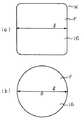
図24にプラスチック材料からなるカード基板1に強誘電体材料を用いた不揮発性強誘電体メモリ(半導体素子)2を搭載した例を示す。ここで、搭載位置が非常に重要となる。すなわち、カード基板は弾性を有するため、外部から印加した物理的ストレスにより「反り」が発生する。図25にその状態を示す。すなわち、カード1の長辺に沿ってFa、Fbの力を印加したとする。なお、FaとFbは絶対値が等しくその向きは逆である。この結果F1、F2、F3の力がカード基板に印加される。これを部分的な領域についてみたのが図26である。
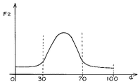
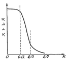
図25及び図26のF2の大きさは、図24に示す位置(長辺方向カード端からの距離)に依存する。すなわち、カードの長辺方向の長さlを100とし、これに対する長辺方向カード端から搭載位置までの距離dとF2の大きさとの関係を示したのが図27である。図27に示すようにF2の大きさは、距離dが両端から30を超えたところから急激に上昇し、70を超えると再び低下する。カード基板と半導体素子もしくはチップ(不揮発性強誘電体メモリ)との間に金属板を介在させてこの半導体素子もしくはチップを安定させることができる。
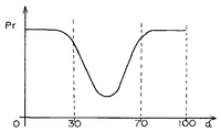
図28には、距離dと残留分極Prとの関係を示す。このように、残留分極Prの大きさはdが両端から30を超えたところから急激に減少し、70を超えると再び上昇する。
【0028】
以上より、カードの強誘電体材料を用いた不揮発性強誘電体メモリ(半導体素子)を搭載する位置は、弾性体カードの端部より30パーセント以内の領域にすべきことが理解される。そして、カードが長方形状の場合は長辺から30パーセント以内ではなく短辺から30パーセント以内であることが望ましい。カード使用者は、長辺方向に力を加えがちであるからである。このカードに送受信用アンテナ等を取り付けこの半導体素子もしくはチップに接続すると図43に示すトランスポンダが形成される。
【0029】
次に、図29乃至図31を参照して第5の実施例を説明する。
前述のように、カード基板に力が加われば当然これに搭載された半導体素子に形成されたメモリセルなどにも同じ様にF2などの外力が働く(図24乃至図26参照)。図29は、トランスポンダに搭載される不揮発性強誘電体メモリ(半導体素子もしくはチップ)のメモリセルの概略平面図である。この半導体素子には複数のメモリセルが行列状にメモリセルアレイの形で配置形成されている。図は、メモリセルアレイの一部を表わしている。メモリセルは、図1に示すように、ゲート20を有するMOSトランジスタとPZTなどからなる強誘電体膜16を有するキャパシタとを備えている。この実施例では、メモリセルの1セルは、2トランジスタ2キャパシタ(2T/2C)から構成されているが、この構成のものに限らず1トランジスタ1キャパシタ(1T/1C)などであっても良い。
この実施例では、キャパシタの強誘電体膜の形状に特徴がある。図29では、斜線で示すキャパシタの強誘電体膜Fは、正方形状である。カード基板に外力が加えられた場合にこれに搭載された半導体素子に形成された強誘電体膜Fに掛かるストレスはその長さに比例する。したがって、強誘電体膜Fの面積が一定の場合長方形状より正方形の方がストレスに強い。ところで、この強誘電体膜に加えられるストレスの大きさは、そのヒステリシス特性に影響を与える。したがって、このようなストレスに強い強誘電体膜を用いると、高いデータ保持特性のメモリカードを得ることができる。
【0030】
図24に示すメモリカードのカード基板1は、略長方形のプラスチック弾性体から構成されている。この実施例の半導体基板に形成された半導体素子2も略長方形である。そして、この半導体素子2は、カード基板1の短辺に近くに、半導体素子2の長辺がこのカード基板1の短辺に平行になるように搭載される。この様に半導体素子2を配置すると半導体素子にストレスが多く掛からなくなる。なお、半導体素子2は、金属板を介して搭載されていても良く、また直接搭載されていても良い。前者ならより高い信頼性が得られ、後者なら低コストであり、かつ極薄なカードが実現できる。とくに、後者はこの実施例の構成を利用することによりはじめて可能となる。
図30は、キャパシタの強誘電体膜の他の形状を示す平面図である。ストレスに強い強誘電体膜には上記正方形状体があるが、この正方形状体の四隅を面取りしたもの(図30(a))、あるいは円形状体(図30(b))がある。面取り体は、正方形の各コーナーに曲率半径Rをつけたものである。この曲率半径Rの大きさによって強誘電体膜に加えられるストレスが変化する。図31は、強誘電体膜に加えられるストレス(F2)の曲率半径R異存性を示す特性図である。正方形の一辺の長さをLとすると、Rが0.1R程度まではストレスは殆ど一定であるが0.2R〜0.3R付近でストレスが急に小さくなり0.5R(すなわち円形体)になってストレスが最小になる。
以上のような形状のストレスに強い強誘電体膜を用いると、図43のトランスポンダに提供される高いデータ保持特性のメモリカードを得ることができる。
【0031】
次に、図32及び図33を参照して第6の実施例を説明する。
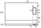
図32は、トランスポンダに搭載される強誘電体メモリセルを備えた不揮発性強誘電体メモリ(半導体素子もしくはチップ)を搭載したメモリカードの平面図及び断面図である。図24に示すカード基板1は、長辺A及び短辺Bのほぼ長方形のプラスチック弾性体から構成されている。本発明の半導体素子が形成された半導体基板2は長辺a及び短辺bのほぼ長方形である。そしてこの半導体素子2は、カード基板1の短辺Bに近くに、半導体素子2の長辺aがこの短辺Bに平行になるように搭載される。
なお、半導体素子2は、金属板3を介して搭載されていてもよく、また、直接搭載されていても良い(この実施例では金属板3を用いている)。前者ならばより高い信頼性が得られ、後者ならは低コスト、極薄カードが実現できる。とくに、後者はこの実施例の構成を利用することによりはじめて可能となる。
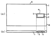
この外力F2の大きさは、半導体素子2の搭載方向に依存する。また、この大きさは、カード基板1の長辺方向の半導体素子の長さに依存する。半導体素子2が形成されるシリコン基板(チップ)は、略長方形状をしており、この長辺aを図32のようにカードの短辺Bに平行に配置した場合は外力がF2が小さく、逆に、図33のように垂直に配置した場合には外力F2が大きくなり、したがってこの配置方法は有利ではない。
上述したように、外力F2の大きさは、強誘電体膜のヒステリシス特性に影響を与える。従って、トランスポンダなどに提供される高いデータ保持特性のメモリカードを得るためには、図33のように搭載するのではなく、図32のように搭載すべきである。
【0032】
次に、図34乃至図38を参照して第7の実施例を説明する。
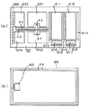
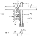
図34(a)にRFIDシステムに必要な回路を1チップに搭載した不揮発性強誘電体メモリ(半導体素子)を示す。図34(b)は、このRFIDシステムに用いるプラスティック材料からなるカード基板にこの半導体素子を搭載したトランスポンダの例である。図34(b)に示すように、プラスティック材料からなるカード基板69の一端に1チップ型の混載不揮発性強誘電体メモリ(半導体素子)60を搭載する。カード基板69の周囲には送受信用アンテナ88がループ状に張り巡らされている。
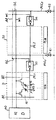
半導体素子60は、図34(a)に示すようような構成とされている。すなわち、半導体素子の一端(好ましくは短辺側)に入出力パッド601の列が配置されている。入出力パッド601の近傍には整流回路633及び検波/送信回路634が配置されている。整流回路633では入力された信号の搬送波からダイオードブリッジ回路等により直流5V電圧を発生する。検波/送信回路634においてはアンテナ88により受信した信号をAM変調であれば、例えば、ヘテロダイン方式で、FM変調であれば、例えば、PLL方式で検波することにより外部から情報を受領し、逆にアンテナ88を用いて外部に情報を送信する。
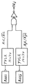
不揮発性強誘電体メモリは、半導体素子の他端(特に整流回路633の反対側)に配置されている。このように配置することにより整流回路で発生する熱を効果的に分散することができる。不揮発性メモリの構成は、以下の通りである。すなわち、不揮発性メモリセルアレイ611、612、行デコード回路614、プレートデコード/駆動回路613、615、センスアンプアレイ616、617、カラム選択回路618、619等から構成される。
【0033】
メモリセルと電源系回路(整流回路633等)との間には各種の制御回路、演算回路等631、632が配置されている。これら演算回路は、ASIC用のスタンダードセル構造であることが設計時間短縮のためにも、さらには効果的な放熱のためにも好ましい。
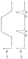
不揮発性強誘電体メモリのメモリセル部(FRAMセル部)と電源系回路との間には電源線が設けられており、電源系回路で発生した直流電圧を不揮発性強誘電体メモリセルに供給する。電源線はVCC(高電位側)電源線84とVSS(低電位側)電源線85からなり、両者の電位差は通常5Vである。そして、本願の特徴である蓄熱手段86、87が電源線の中間に配置されている。この蓄熱手段86、87は、電源線に設けられた素材と同一部材(アルミニウムが好ましい)からなる突出部であり、以下これをローブと称する。
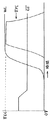
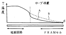
図35にローブを設けたことによる効果を説明する特性図を示す。図35の縦軸は、温度を示し、横軸は、半導体素子上の整流回路などの電源系回路とFRAM部との間の位置(d)を示しており、図35は、半導体素子上の温度分散の状態を示している。図に示すように、もしローブが存在しない場合(点線で示す曲線B)は、比較的高温になり易い電源系回路部からFRAMセル部に何の障害も無しに熱が伝達され、メモリセルの温度が上昇してしまう。これは前述のようにデータ保持特性の劣化につながり得るものである。このときの温度分布を点線による曲線Bで示す。ローブを設けた場合の温度分布は実線による曲線Aで示されている。実際に用いた形状は、アルミニウム配線VCC/VSSがそれぞれ厚さ1.1μm、幅10μmでローブの形状が150×900μmの長方形状のものである。このようにローブを設けることにより熱伝達が急峻に変化するのは、おそらく電源線が熱伝達の主要な役割をしめていたことに起因するものと思われる。
【0034】
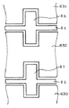
図36にローブの変形例を示す。電源線、ローブ等上述と同様の記号を付してある。630は、演算回路、制御回路等を示す。このようにVCC線とVSS線との間に一定程度の間隔をおいて配置し、ローブを左右に広げる形にすることによりより効果的な熱遮断が可能となる。
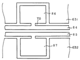
図37は、ローブ86、87と電源線84、85との間にネック(くびれ部)70を設けた例である。通常無電源ID装置の電源回路が動作する時間はそれほど長くない(1秒以下)が例外的に多大なデータ処理が必要になる場合等は動作時間が数秒になることがある。このような場合、ローブの熱容量がすぐに飽和してしまうのを防ぐ必要があり、長時間動作が可能な無電源IDにおいては図37の構成が好ましい。電源線、ローブ等は前述と同様の記号を付してある。
図38(a)は、ローブを制御回路等のトランジスタに電源を供給するためのコンタクト部と共用した例である。すなわち、電源線84にはローブ86が設けられているが、このローブにはその下に配置されたトランジスタ(ソース74、ドレイン75、ゲート73)のソース電源供給用のコンタクトホール72が設けられている。図38(b)はその等価回路を示している。このように構成するとチップ面積の縮小化が図れる。
以上の実施例はPZT強誘電体膜を例にとって説明したが、本発明はこれに限るものではなく、図39に示す通り、例えば、BaTiO3 (BTO)膜等にも適用可能である。また、当然のことながらPLZT膜、LiNbO3 膜、K3 Li2 Nb5 O15膜も適用可能である。
【0035】
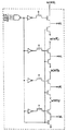
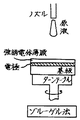
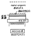
次に、図40乃至図42を参照して強誘電体薄膜製造プロセスを説明する。強誘電体薄膜の製造には、例えば、ゾル・ゲル法、スパッタ法、MOCVD法等が用いられる。本発明と組み合わせてより顕著な効果が得られるのはゾル・ゲル法及びスパッタ法である。
ゾルゲル法又はMOD法は、有機金属化合物などをソース原料とする溶液をディッピングやスピンコートにより基板上に塗布し、それを熱分解して得る方法である。これは、大気中でも成膜が可能であり、膜の大面積化が容易である(図40)。
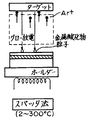
スパッタ法は、薄膜となるべき材料のターゲットに、グロー放電中でイオン化したガス(Arガスなど)を衝突させて叩き出した粒子を基板に堆積させる方法であり、真空蒸着法では作りにくい高融点材料などの膜形成が可能である。この成膜法には直流スパッタ、高周波(RF)スパッタ、マグネトロンスパッタ、イオンビームスパッタ、反応性スパッタ、レーザアブレーションなどがある。ターゲットとしては焼結体又は粉末を用い、アルゴンと酸素雰囲気でスパッタする。ターゲットの近傍にマグネットを置くと、スパッタイオンは、その磁場に拘束され、低ガス圧(〜10−4Torr)でスパッタが可能になり、膜成長速度を数倍高めることになる。
【0036】
強誘電体膜の微細構造と特性は、スパッタ条件(スパッタ電圧、ガス組成とガス圧、膜形成速度、基板材料、基板温度など)に依存する(図41)。
CVDの基本は、薄膜にしたい元素の化合物のうちでガスになるものを高温炉の中に導入して、基板表面に堆積させて膜形成することにあり、これにより基板表面で平衡状態で成膜されるため、より均質な結晶膜が得られる可能性がある。MOCVDは、原料としてアセチルアセトナトやアルコキシドなどの有機金属から強誘電体膜が形成されている(図42)。
本発明は、上記したような半導体基板上に強誘電体メモリセルを形成する場合に限らず、SOIなどのように絶縁基板上の半導体層上に強誘電体メモリセルを形成する場合にも適用することが可能である。また、本発明は、前記実施例の他種々変形して実施することが可能である。
【0037】
【発明の効果】
以上、本発明のトランスポンダに搭載される不揮発性強誘電体メモリは、以上のような構成を有することによりプレート線のCR(容量・抵抗)を低減し、誤動作を引き起こす恐れを防止することができる。
また、本発明は、強誘電体膜をキャパシタに用いた不揮発性強誘電体メモリのプレート線を行方向に複数に分割し、これをそれぞれ駆動する構成において、分割したプレート線の駆動タイミングをずらすことにより一時的に流れる最大電流を減少させることができる。
また、本発明は、分割したプレート線に付設されるプレート線駆動回路がシャント領域に配置されているのでワード線の抵抗を低下させながらチップ面積を小さくすることができる。
【図面の簡単な説明】
【図1】本発明の強誘電体メモリセル(FRAMセル)の断面図。
【図2】強誘電体薄膜の印加電圧/分極特性を示す特性図。
【図3】FRAMセルとして好ましくない状態のヒステリシス特性図。
【図4】書き込み動作を説明するFRAMセルの回路図。
【図5】FRAMセルの書き込み時のプレート電極PLの電位変化図。
【図6】本発明のFRAMセルアレイと周辺回路との配置を示すブロック図。
【図7】本発明のFRAMセルアレイと周辺回路との配置を示すブロック図。
【図8】本発明に用いるプレートデコーダの回路図。
【図9】本発明のプレートデコーダの入力信号を形成する回路の回路図。
【図10】本発明のプレートデコーダの入力信号を形成する回路の回路図。
【図11】本発明に用いるプレートデコーダの回路図。
【図12】本発明のプレートデコーダの入力信号形成回路及び入力信号を示す図。
【図13】本発明のプレートデコーダの入力信号のタイミング図。
【図14】本発明に用いるロウデコーダの回路図。
【図15】本発明のFRAMセルアレイと周辺回路との配置を示す回路図。
【図16】本発明のFRAMセルアレイと周辺回路の詳細な構造を示す部分回路図。
【図17】本発明及び従来のプレート線の動作図。
【図18】本発明の遅延線チェインの回路図。
【図19】本発明のメモリセルアレイと周辺回路の詳細な構造を示す部分回路図。
【図20】本発明のプレート線選択回路の回路図。
【図21】図20の詳細な回路図。
【図22】図19に示すロウデコーダの詳細な回路図。
【図23】本発明のワード線とプレート線の配置を示す配線回路図。
【図24】本発明の半導体素子をプラスチック材料からなるカード基板の平面図。
【図25】外部から印加した物理的ストレスにより「反り」が発生したカード基板の断面図。
【図26】図25の部分的な領域の拡大断面図。
【図27】長辺方向カード端から搭載位置までの距離dとF2の大きさとの関係を示す特性図。
【図28】カード基板上の距離dとヒステリシス曲線における残留分極Prとの関係を示す特性図。
【図29】本発明の半導体素子に形成されたメモリセルアレイの部分平面図。
【図30】本発明のメモリセルのキャパシタの強誘電体膜の形状を示す平面図。
【図31】本発明の強誘電体膜の角部の曲率半径の大きさと強誘電体膜に掛かるストレスとの関係を示す特性図。
【図32】本発明の半導体素子が搭載されたカード基板の平面図及び断面図。
【図33】本発明の半導体素子が搭載されたカード基板の平面図及び断面図。
【図34】本発明のRFIDシステムに必要な回路を搭載した半導体素子の平面図及びカード基板にこの半導体素子を搭載した平面図。
【図35】本発明のローブを設けたことによる効果を説明する特性図。
【図36】本発明のローブの配置を示す半導体素子の部分平面図。
【図37】本発明のローブの配置を示す半導体素子の部分平面図。
【図38】本発明のローブの配置を示す半導体素子の部分平面図及び回路図。
【図39】本発明に用いる強誘電体膜の特性を示す特性図。
【図40】本発明の強誘電体薄膜製造プロセス図。
【図41】本発明の強誘電体薄膜製造プロセス図。
【図42】本発明の強誘電体薄膜製造プロセス図。
【図43】RFIDシステムのシステム構成図、トランスポンダ斜視図及びRFIDチップの平面図。
【図44】トランスポンダの内部回路図。
【図45】従来のFRAMセルと周辺回路との配置を示すブロック図。
【図46】FRAMセルのヒステリシス特性図。
【図47】強誘電体メモリのプレート線を駆動する電圧及び電流特性図。
【符号の説明】
1、69・・・カード基板、 2、60・・・半導体素子、
3・・・金属板、 10・・・シリコン基板、
11、75・・・ドレイン領域、 12、74・・・ソース領域、
13・・・素子分離絶縁膜、 14、18・・・層間絶縁膜、
15・・・下層電極、 16・・・強誘電体膜(PZT膜)、
17・・・上層電極、 19・・・接続配線、
20、73・・・ゲート電極、 21・・・ゲート絶縁膜、
22、72・・・コンタクトホール、 30・・・メモリセル、
31、32、33、34、611、612・・・メモリセルアレイ、
35、36、37、38・・・プレート線選択回路、
40・・・ロウデコーダ回路、
41、42、43、44・・・センスアンプ回路、
51、52、53、54・・・カラムゲート回路、 55・・・データ線、
56・・・カラムデコード回路、 57・・・データ線センスアンプ回路、
58・・・FSK復調回路、 59・・・整流ブリッジ、
60・・・パワーオン回路、
61、62、63、64、65・・・プレート線制御線駆動回路、
66、67、68・・・遅延線チェイン、
70・・・ローブのくびれ部、 84・・・VCC電源線、
85・・・VSS電源線、 86、87・・・ローブ(蓄熱手段)、
88・・・送信兼受信アンテナ、 411・・・センスアンプ、
412・・・イコライズ回路、 601・・・入出力パッド、
613、615・・・プレートデコード/駆動回路、
614・・・行デコード回路、 616、617・・・センスアンプアレイ、
618、619・・・カラム選択回路、
630、631、632・・・演算回路、 633・・・整流回路、
634・・・検波/送信回路。[0001]
BACKGROUND OF THE INVENTION
The present invention relates to a transponder used in an RFID system, and in particular, a nonvolatile ferroelectric memory mounted on a transponder and having an array of memory cells using a ferroelectric film as an information storage capacitor, a driving method thereof, and an ID It is about the card.
[0002]
[Prior art]
An RFID (Radio Frequency Identification) system is a non-contact type tag system (identifier) using radio waves, and includes a host side including a personal computer, a controller, an antenna, and the like, and a transponder. The transponder is mounted with a chip such as a nonvolatile ferroelectric memory.
In recent years, a nonvolatile ferroelectric memory using a ferroelectric memory cell has been actively researched and developed as a semiconductor memory device with low power consumption. This nonvolatile ferroelectric memory is disclosed in U.S. Pat. No. 4,873,664 (Eaton, Jr.) and S.A. S. Eaton, Jr. et al. “A Ferroelectric DRAM Cell for High Density NVRAMs”, ISSCC Digest of Technical Papers, pp. 130-131, Feb. 1988 and the like.
Barium titanate (BaTiO 3) is used as an information storage capacitor in a ferroelectric memory cell. 3 ), Lead zirconate titanate (Pb (Zr, Ti) O) 3 PZT), lanthanum doped lead zirconate titanate ((Pb, La) (Zr, Ti) O 3 PLZT), lithium niobate (LiNbO) 3 ), Potassium lithium niobate (K 3 Li 2 Nb 5 O 15 ) Or the like is used. These ferroelectric films are polarized by applying a voltage. The relationship between voltage and polarization exhibits a so-called hysteresis characteristic.
[0003]
With regard to this relationship, the inventors measured the characteristics of the ferroelectric film and found that physical stress applied from the outside affects the hysteresis characteristics described above. In other words, it was found that when a physical stress is applied to the ferroelectric film after the film formation, the hysteresis loop becomes small and the polarization holding characteristic deteriorates. Ferroelectric memories use polarization for data retention. Therefore, it is clear that physical stress applied from the outside leads to deterioration of data retention characteristics.
FIG. 45A shows an arrangement of a memory cell array and peripheral circuits of a conventional nonvolatile semiconductor memory device. A plurality of memory cell arrays are arranged in parallel, and a row decoder (RD) (word line selection circuit) 40 is shared by them. The plurality of word lines WL are selected by the
[0004]
[Problems to be solved by the invention]
As described above, the nonvolatile ferroelectric memory used in the conventional transponder has a large CR (capacitance / resistance) when the plate line is decoded (pulse-driven), so that the plate line operates with a delay. There is a possibility that the data written in the cell cannot be sufficiently read or the data cannot be sufficiently written in the cell. Further, the word line is only connected to the gate of the transistor of the memory cell, whereas the plate line is commonly connected to the counter electrode of the cell capacitor as described above, so that the additional capacitance is very large. As a result, it takes more time to drive the plate line than when the word line is driven. Since the plate line signal rises and falls in a short time, the information reading speed of the memory cell is limited by the pulse of the plate line signal. Therefore, it is necessary to increase the signal speed of the plate line.
In particular, when a nonvolatile ferroelectric memory is mounted on a memory card or the like, there is a problem that when the memory card is thin, physical stress is easily applied from the outside, and as a result, data retention characteristics deteriorate.
[0005]
However, it is known that the shape of this hysteresis characteristic varies greatly with temperature. That is, the hysteresis loop at a high temperature (for example, 80 ° C.) becomes smaller than that at a low temperature (for example, 25 ° C., which is room temperature), and the polarization holding characteristics deteriorate. Ferroelectric memories use polarization for data retention. Therefore, the presence of a heat source in the chip leads to deterioration of data retention characteristics.
In particular, when a nonvolatile ferroelectric memory is mounted on a non-power source memory card or the like, heat generated in a power supply circuit, a rectifier circuit, or the like may affect the data retention characteristics of the ferroelectric memory.
FIG. 46 is a hysteresis curve of a ferroelectric material used for a memory cell (FRAM cell) using a ferroelectric film as a capacitor. When writing and reading operations are performed, the state is changed along the edge of the curve in the order of a → b → c → d. However, the current actually flows at b and d. The current required to reverse the polarization of the cell flows only at b and d. Therefore, even when the plate line PL is driven as shown in FIG. 47A, almost no current flows in the first half of the rise of the plate line PL, whereas in the second half, a current flows in a pulse manner (FIG. 47B). . Thus, when current flows intensively in an extremely short time, the maximum amount of current increases, and as a result, various malfunctions may occur due to fluctuations in the power supply potential and variations in the reference potential caused thereby.
[0006]
The present invention has been made in view of the above circumstances, and includes a plate line having a structure in which the drive speed is improved by preventing the possibility of causing a malfunction when the plate line is decoded (pulse drive), A non-volatile ferroelectric memory mounted on a transponder is provided.
The present invention also provides a nonvolatile ferroelectric memory that can reduce the maximum amount of drive current flowing through the plate line while improving the drive speed of the plate line, and a method for driving the same.
[0007]
[Means for Solving the Problems]
In the nonvolatile ferroelectric memory of the present invention, memory cells in which a capacitor for information storage using a ferroelectric as an interelectrode insulating film and a MOS transistor for charge transfer are connected in series are arranged in a matrix. A plurality of word lines connected in common to the gates of the MOS transistors of the same memory cell, a plurality of plate lines connected in common to one end of the capacitor of the same memory cell, The word line and the plate line are arranged in parallel, and a plurality of plate lines are further divided with respect to the corresponding word line, and each is connected in common to one end of the MOS transistor of the same memory cell A plurality of bit lines; a word line selection circuit for selecting a part of the plurality of word lines based on an address signal; Plate line selection circuit formed by an external terminal such as a chip enable (Chip Enable) signal (/ CE), and the plate line selection circuit for each word line. It is characterized by the presence of a plurality. Further, the plurality of plate selection circuits corresponding to the word lines operate independently according to the address signal, and all the plate selection circuits do not operate during normal operation.
Each word line of the plurality of word lines has a plurality of plate line selection circuits (plate decoders), has divided plate lines, and partially decodes each, for example, a column address signal Therefore, it is not a plate line with a large CR, and the possibility of malfunctioning with a sufficient operating margin is reduced.
[0008]
The present invention also provides a configuration in which a plate line of a nonvolatile ferroelectric memory using a ferroelectric film as a capacitor is divided into a plurality of rows in the row direction and the drive timing of the divided plate lines is shifted in a configuration in which the plate line is driven. Is characterized in that the current flowing temporarily is reduced.
The nonvolatile ferroelectric memory of the present invention includes a memory cell array in which ferroelectric memory cells using a ferroelectric film as an information storage capacitor are arranged in a matrix, and gates of transistors of memory cells in the same row. A word line formed in common; a plate line formed by commonly connecting counter electrodes of capacitors of memory cells in the same row; and a row decoder that selects and drives the word line, the plate line extending in a row direction. It is divided into n, n plate line selection circuits are respectively connected to one end thereof, and the gate capacitance of the transistor of the memory cell is smaller than the capacitor capacitance of the memory cell.
[0011]
DETAILED DESCRIPTION OF THE INVENTION
Hereinafter, embodiments of the present invention will be described with reference to the drawings.
The RFID system is a non-contact type tag system (identifier) using radio waves, and is generally called a non-contact data carrier system. The present invention relates to a transponder used in this system, a nonvolatile ferroelectric memory mounted on the transponder, and a driving method thereof.
FIG. 43 is a system configuration diagram of the entire RFID system using the transponder of the present invention. The RFID system includes a host side including a personal computer, a controller, an antenna, and the like, and a data carrier called a transponder (FIG. 43A). The transponder has a simple configuration in which a monolithic RFID chip in which a FRAM and an ASIC are integrated into a single chip on a card substrate and an antenna for both power reception and data reception / transmission are built in (FIG. 43B). FIG. 43C is a plan view of the monolithic RFID chip. From the host side, commands and data are transmitted on a carrier wave as necessary. On the transponder side, necessary power is generated by the carrier wave, and information is returned to the host side for data writing, reading and transmission. . The non-contact tag does not require a battery, and can be used for management of human entry and exit by reading the stored contents of the FRAM in a non-contact manner using radio waves and rewriting the contents. For example, a ticket gate with a non-contact tag for commuter passes in the pocket of clothes, a non-contact tag attached to a car, running without paying off at a tollgate on a highway, It can be used for purposes such as monitoring and managing parking lot entry and exit without intervention. It can also be used to manage migratory fish and livestock behavior.
[0012]
FIG. 44 shows details of the internal circuit of the transponder. An LC circuit that detects an electromagnetic field input from the outside, a circuit that generates a signal from the electromagnetic field detected by the LC circuit (FSK demodulation circuit) 58, and a circuit that generates a power supply voltage from the electromagnetic field detected by the LC circuit (rectifier bridge) 59, a plurality of memory cells including a power-on
[0013]
Next, a first embodiment will be described with reference to FIGS.
FIG. 1 shows a cross-sectional view of a nonvolatile ferroelectric memory mounted on a transponder. This ferroelectric memory is used by being mounted on a transponder as shown as a monolithic RFID chip in FIG. An element isolation insulating film 13 made of a silicon oxide film is formed on the surface of the P-
[0014]
FIG. 2 shows applied voltage / polarization characteristics of a ferroelectric thin film such as a PZT film. The ferroelectric thin film has a hysteresis characteristic as shown in FIG. Then, data can be stored depending on whether the remanent polarization Pr is “positive” or “negative” when no voltage is applied, that is, when V = 0 (V).
FIG. 3 shows hysteresis characteristics which are not preferable for a ferroelectric memory cell of a nonvolatile ferroelectric memory. That is, there are problems such that the remanent polarization Pr is very small, and as a result, the read margin by the sense amplifier is reduced, and data is easily lost due to external disturbance. The characteristics shown in FIG. 3 are hysteresis characteristics at a high temperature of 80 ° C.
Subsequently, a write operation of the memory cell using the ferroelectric thin film will be described with reference to FIGS. A nonvolatile ferroelectric memory using FRAM cells constitutes one memory cell by two MOS transistors Q1 and Q2 and ferroelectric capacitors C1 and C2. 4A, that is, the capacitor C1 has an upward polarization (hereinafter referred to as positive polarization) as indicated by an upward arrow in the figure, and the capacitor C2 has an downward arrow in the figure. A state in which downward polarization (hereinafter referred to as negative polarization) appears is defined as “1”, and the state of FIG. 4B, that is, the capacitor C1 has negative polarization and the capacitor C2 has positive polarization. The state that appears is defined as “0”.
[0015]
("1" write operation)
The steps for writing “1” to the memory cell are shown below.
First, 5 V is applied to the bit line BL, and 0 V is applied to the bit line / BL (“/” represents an inverted signal, hereinafter the same). Then, 7V is applied to the word line WL, and 0V is applied to the plate electrode PL. In this state, the capacitor C1 is in the state shown in FIG. 2a, and the capacitor C2 is in the state shown in FIG. 2b.
Subsequently, PL is set to 5V. As a result, the capacitor C1 is in the state of b in FIG. 2, and the capacitor C2 is in the state of c in FIG.
Subsequently, PL is set to 0V. As a result, the capacitor C1 is in the state of FIG. 2a, and the capacitor C2 is in the state of d in FIG.
FIG. 5 shows changes in the potential (VPL) of the plate electrode PL during writing.
As described above, the state of FIG. 4A, that is, the positive polarization appears in the capacitor C1, and the negative polarization appears in the capacitor C2, thereby realizing “1” writing.
[0016]
("0" write operation)
The steps for writing “0” to the memory cell will be described below.
First, 0 V is applied to the bit line BL, and 5 V is applied to the bit line / BL. Then, 7V is applied to the word line WL, and 0V is applied to the plate electrode PL. In this state, the capacitor C1 is in the state shown in FIG. 2b, and the capacitor C2 is in the state shown in FIG.
Subsequently, PL is set to 5V. As a result, the capacitor C1 is in the state of c in FIG. 2, and the capacitor C2 is in the state of b in FIG.
Subsequently, PL is set to 0V. As a result, the capacitor C1 is in the state of d in FIG. 2, and the capacitor C2 is in the state of a in FIG.
As described above, the state shown in FIG. 4B, that is, negative polarization appears in the capacitor C1, and positive polarization appears in the capacitor C2, thereby realizing “0” writing.
[0017]
Since the nonvolatile ferroelectric memory as described above consumes little power, it is used for a non-power source ID device or the like. The non-powered ID device uses a DC voltage obtained by receiving a radio wave from the outside and rectifying the radio wave as a power source, and receiving and detecting the information as the radio wave carrier signal to input data to the outside. Output. A non-power supply ID device is usually equipped with a radio wave transmission circuit. When configured as described above, the ID card can be configured without a power source, and information can be exchanged with the outside without any contact with the parent device. The non-powered ID card as described above is expected to be applied to a license, a product tag, an identification card, a commuter pass, a ski lift ticket, and the like.
Next, FIG. 6 and FIG. 7 show the arrangement of the memory cell array and peripheral circuits of the nonvolatile ferroelectric memory. The
[0018]
The word line WL is selected by the
The circuit shown in FIG. 8 is the plate decoder of the present invention. The plate decoder includes a NAND circuit and an inverter circuit to which an output signal of the NAND circuit is input. The inverter circuit supplies a power supply voltage (Vcc) as a plate voltage (VPL). As an input signal of the NAND circuit, the φ6 signal is a signal having a delay signal and a pulse from / CE (Chip Enable signal) (/ RAS in the case of DRAM) (see FIG. 9). The Yα signal is a partial address signal and is an address related to the horizontal direction. Further, WL indicates the corresponding word line. Here, for example, in the memory cell array shown in FIGS. 6 and 7, there are four divided plate lines PL for one word line WL. Therefore, one of the four plate lines is selected by this address signal (Yα). As a result, the capacity is at least 1/4 that of the conventional plate line, so that the plate line can be decoded at a high speed and malfunction can be prevented.
[0019]
FIG. 11 shows another embodiment of the plate decoder. For example, if there are two addresses i and j, complementary signals Aic // Aic and Ajc // Ajc are generated by the address buffer (see FIG. 10). When a precoder is created using this, the result is as shown in FIG. There are four types of input methods shown in FIG. By this method, four Yα signals (Yα0, Yα1, Yα2, Yα3) are generated. When these four Yαj signals are input to the plate decoder of FIG. 11, one VPL among the four plate voltages (VPL) can be pulse-driven. The input signals (WL, VPL, / CE (φ6)) of the plate decoder of FIGS. 8 and 11 have voltage waveforms as shown in the timing chart of FIG.
A detailed circuit diagram of the row decoder shown in FIGS. 6 and 7 is shown in FIG. The row decoder is a circuit that selects a word line. A set of decoders is selected by signals Xαj, Xαk, and Xαl obtained by predecoding row addresses. Four word lines are connected to one set of decoders, and one of them is selected by signals WDRVi to WDRVl.
[0020]
FIG. 15 shows details of the sense amplifier used in the memory cell array of FIGS. FIG. 15 shows details of the
[0021]
Next, a second embodiment will be described with reference to FIGS.
FIG. 16 is a partial circuit diagram showing a detailed structure of a memory cell array and peripheral circuits of a nonvolatile ferroelectric memory (FRAM) mounted on a transponder.
[0022]
The feature of this embodiment is that, as shown in FIG. 16, in the configuration in which the memory cell array is divided into a plurality and the plate lines are divided and driven, the maximum current that flows temporarily is reduced by shifting the drive timing of the plate lines. is there. As shown in the figure, for example, plate lines PL (PL1 to PL4) that are independently driven and controlled are arranged in four blocks, and a plate line control
In this embodiment, adjustment of the delay time of the delay line is important. If the delay time is long, read and write cycles become long, and it becomes impossible to provide a high-speed memory. As described above, in the FRAM, current flows only in pulses only in the latter half of the rise or fall of the plate line. Therefore, the rising or falling time of each plate line may overlap. More specifically, it takes 5 ns for each plate line to rise. However, the current actually flows in the last 0.5 ns. Therefore, in this case, 4.5 ns may be overlapped. Therefore, the delay time of the delay line is determined to be 0.5 ns or more. More generally, assuming that the rise time of the plate line is t and rises to the ramp state, it is known that a current does not flow in about 90% of the time and a large amount of current flows in the remaining 10%. As a result, a delay time of 1/10 or more may be set. An example of the delay line is shown in FIG. The delay line is generally configured by connecting inverter circuits in series. However, if the delay time is shorter than 1 ns, only metal wiring may be sufficient. 18A and 18B show an example of an inverter circuit, and FIG. 18C shows an example of a metal wiring such as aluminum.
[0023]
Next, a third embodiment will be described with reference to FIGS.
FIG. 19 is a partial circuit diagram showing a detailed structure of a memory cell array and peripheral circuits of a nonvolatile ferroelectric memory mounted on a transponder.
[0024]
A plate line control line is connected to one of two inputs of the NAND circuit of the plate line selection circuit, and a gate line is connected to the other.
The gate capacitance (C1) of the memory cell transistor is smaller than the capacitor capacitance (C2) of the memory cell (C1 <C2).
FIG. 20 is a circuit diagram of the plate
FIG. 21 is a detailed circuit diagram of FIG. 20, and the inverter circuit includes an N-channel transistor N2 and a P-channel transistor P2. In this embodiment, the power supply voltage Vcc is 5V.
FIG. 22 is a detailed circuit diagram of the row decoder (RD) 40 shown in FIG. As shown in FIG. 22, the product of the gate width / length ratio ((W / L) 1) of the transistor in the
[0025]
As shown in FIG. 22, the row decoder has an inverter configuration in which a P-channel transistor P1 and an N-channel transistor N1 are directly connected to the final stage, and the plate
[0026]
Further, the gate width / length ratio ((W / L) n1) of the N channel transistor N1 in the row decoder RD is equal to the gate width / length ratio ((W / L) n1) in the row decoder RD. L) is configured smaller than p1) ((W / L) n1 <W / L) p1. Further, the gate width / length ratio ((W / L) n2) of the N-channel transistor N2 in the plate
As shown in FIG. 23, the metal wiring word line Al-WL is shunt-connected to the word line WL. The shunt lines SL are arranged at regular intervals. In the present invention, for each predetermined shunt line SL, the shunt line SL and a plate
[0027]
Next, a fourth embodiment will be described with reference to FIGS.
FIG. 24 shows an example in which a nonvolatile ferroelectric memory (semiconductor element) 2 using a ferroelectric material is mounted on a
The size of F2 in FIGS. 25 and 26 depends on the position shown in FIG. 24 (distance from the card edge in the long side direction). That is, FIG. 27 shows the relationship between the distance d from the end of the long side card to the mounting position and the size of F2, where the length l in the long side of the card is 100. As shown in FIG. 27, the magnitude of F2 increases rapidly when the distance d exceeds 30 from both ends, and decreases again when it exceeds 70. The semiconductor element or chip can be stabilized by interposing a metal plate between the card substrate and the semiconductor element or chip (nonvolatile ferroelectric memory).
FIG. 28 shows the relationship between the distance d and the remanent polarization Pr. As described above, the magnitude of the remanent polarization Pr rapidly decreases when d exceeds 30 from both ends, and increases again when it exceeds 70.
[0028]
From the above, it is understood that the position where the nonvolatile ferroelectric memory (semiconductor element) using the ferroelectric material of the card is to be mounted should be within a region within 30 percent from the end of the elastic card. And when a card | curd is rectangular shape, it is desirable for it to be within 30 percent from a short side instead of within 30 percent from a long side. This is because the card user tends to apply force in the long side direction. When a transmitting / receiving antenna or the like is attached to this card and connected to this semiconductor element or chip, a transponder shown in FIG. 43 is formed.
[0029]
Next, a fifth embodiment will be described with reference to FIGS.
As described above, when a force is applied to the card substrate, naturally, an external force such as F2 similarly acts on a memory cell formed on a semiconductor element mounted on the card substrate (see FIGS. 24 to 26). FIG. 29 is a schematic plan view of a memory cell of a nonvolatile ferroelectric memory (semiconductor element or chip) mounted on a transponder. In this semiconductor element, a plurality of memory cells are arranged and formed in a matrix in the form of a memory cell array. The figure shows a part of the memory cell array. As shown in FIG. 1, the memory cell includes a MOS transistor having a
This embodiment is characterized by the shape of the ferroelectric film of the capacitor. In FIG. 29, the ferroelectric film F of the capacitor indicated by hatching has a square shape. When an external force is applied to the card substrate, the stress applied to the ferroelectric film F formed on the semiconductor element mounted on the card substrate is proportional to its length. Therefore, when the area of the ferroelectric film F is constant, the square shape is more resistant to stress than the rectangular shape. By the way, the magnitude of the stress applied to the ferroelectric film affects its hysteresis characteristics. Therefore, if a ferroelectric film resistant to such stress is used, a memory card having high data retention characteristics can be obtained.
[0030]
A
FIG. 30 is a plan view showing another shape of the ferroelectric film of the capacitor. The ferroelectric film resistant to stress includes the above-mentioned square-shaped body, and there is a chamfered corner (FIG. 30 (a)) or a circular-shaped body (FIG. 30 (b)). The chamfered body is obtained by adding a radius of curvature R to each corner of a square. The stress applied to the ferroelectric film varies depending on the radius of curvature R. FIG. 31 is a characteristic diagram showing the curvature radius R heterogeneity of the stress (F2) applied to the ferroelectric film. If the length of one side of the square is L, the stress is almost constant until R is about 0.1R, but the stress suddenly decreases in the vicinity of 0.2R to 0.3R and becomes 0.5R (that is, a circular body). The stress is minimized.
If a ferroelectric film resistant to stress having the above shape is used, a memory card having high data retention characteristics provided to the transponder shown in FIG. 43 can be obtained.
[0031]
Next, a sixth embodiment will be described with reference to FIGS. 32 and 33. FIG.
FIG. 32 is a plan view and a sectional view of a memory card on which a nonvolatile ferroelectric memory (semiconductor element or chip) having a ferroelectric memory cell mounted on a transponder is mounted. A
The
The magnitude of the external force F2 depends on the mounting direction of the
As described above, the magnitude of the external force F2 affects the hysteresis characteristics of the ferroelectric film. Therefore, in order to obtain a memory card with high data retention characteristics provided to a transponder or the like, it should be mounted as shown in FIG. 32, not as shown in FIG.
[0032]
Next, a seventh embodiment will be described with reference to FIGS.
FIG. 34A shows a nonvolatile ferroelectric memory (semiconductor element) in which a circuit necessary for the RFID system is mounted on one chip. FIG. 34B shows an example of a transponder in which this semiconductor element is mounted on a card substrate made of a plastic material used in this RFID system. As shown in FIG. 34B, a one-chip mixed nonvolatile ferroelectric memory (semiconductor element) 60 is mounted on one end of a
The
The nonvolatile ferroelectric memory is disposed on the other end of the semiconductor element (particularly on the opposite side of the rectifier circuit 633). By arranging in this way, the heat generated in the rectifier circuit can be effectively dispersed. The configuration of the nonvolatile memory is as follows. That is, the memory cell array includes non-volatile
[0033]
Various control circuits and
A power supply line is provided between the memory cell portion (FRAM cell portion) of the nonvolatile ferroelectric memory and the power supply system circuit, and a DC voltage generated by the power supply system circuit is supplied to the nonvolatile ferroelectric memory cell. To do. The power source line is composed of a VCC (high potential side)
FIG. 35 is a characteristic diagram for explaining the effect of providing a lobe. The vertical axis in FIG. 35 indicates temperature, and the horizontal axis indicates the position (d) between the power supply system circuit such as a rectifier circuit on the semiconductor element and the FRAM unit. FIG. The state of temperature dispersion is shown. As shown in the figure, if there is no lobe (curve B indicated by a dotted line), heat is transferred from the power supply system circuit portion, which is likely to be relatively high temperature, to the FRAM cell portion without any trouble, and the memory cell The temperature will rise. As described above, this can lead to deterioration of data retention characteristics. The temperature distribution at this time is indicated by a curved line B with a dotted line. The temperature distribution in the case where the lobe is provided is shown by a curved line A with a solid line. The shape actually used is a rectangular shape in which the aluminum wiring VCC / VSS is 1.1 μm thick, the width is 10 μm, and the lobe shape is 150 × 900 μm. Such a steep change in heat transfer due to the provision of the lobe is probably due to the fact that the power line played a major role in heat transfer.
[0034]
FIG. 36 shows a modification of the lobe. Symbols similar to those described above, such as power lines and lobes, are attached.
FIG. 37 shows an example in which a neck (constriction portion) 70 is provided between the
FIG. 38A shows an example in which a lobe is shared with a contact portion for supplying power to a transistor such as a control circuit. That is, the
In the above embodiment, the PZT ferroelectric film has been described as an example. However, the present invention is not limited to this. For example, as shown in FIG. 3 It can also be applied to (BTO) films. Of course, PLZT film, LiNbO 3 Membrane, K 3 Li 2 Nb 5 O 15 A membrane is also applicable.
[0035]
Next, a ferroelectric thin film manufacturing process will be described with reference to FIGS. For the production of the ferroelectric thin film, for example, a sol-gel method, a sputtering method, an MOCVD method or the like is used. In combination with the present invention, the sol-gel method and the sputtering method are more effective.
The sol-gel method or the MOD method is a method obtained by applying a solution using an organometallic compound or the like as a source material on a substrate by dipping or spin coating, and thermally decomposing it. This can be formed even in the atmosphere, and the area of the film can be easily increased (FIG. 40).
Sputtering is a method of depositing on the substrate particles that have been struck by colliding ionized gas (such as Ar gas) in a glow discharge against a target of a material that should be a thin film. Film formation of materials and the like is possible. Examples of the film forming method include direct current sputtering, radio frequency (RF) sputtering, magnetron sputtering, ion beam sputtering, reactive sputtering, and laser ablation. A sintered body or powder is used as a target, and sputtering is performed in an argon and oxygen atmosphere. When a magnet is placed in the vicinity of the target, the sputter ions are restrained by the magnetic field, and a low gas pressure (−10 -4 (Torr) enables sputtering and increases the film growth rate several times.
[0036]
The microstructure and characteristics of the ferroelectric film depend on sputtering conditions (sputtering voltage, gas composition and gas pressure, film formation rate, substrate material, substrate temperature, etc.) (FIG. 41).
The basis of CVD is to introduce a compound of the element to be thinned into a gas into a high temperature furnace and deposit it on the substrate surface to form a film, thereby forming an equilibrium state on the substrate surface. Since the film is formed, a more uniform crystal film may be obtained. In MOCVD, a ferroelectric film is formed from an organic metal such as acetylacetonate or alkoxide as a raw material (FIG. 42).
The present invention is not limited to the case where the ferroelectric memory cell is formed on the semiconductor substrate as described above, but is also applied to the case where the ferroelectric memory cell is formed on the semiconductor layer on the insulating substrate such as SOI. Is possible. The present invention can be implemented with various modifications in addition to the above-described embodiments.
[0037]
【The invention's effect】
As described above, the nonvolatile ferroelectric memory mounted on the transponder according to the present invention has the above-described configuration, thereby reducing the CR (capacitance / resistance) of the plate line and preventing the possibility of malfunction. .
Further, according to the present invention, a plate line of a nonvolatile ferroelectric memory using a ferroelectric film as a capacitor is divided into a plurality of rows in the row direction, and the drive timing of the divided plate lines is shifted in a configuration in which each is driven. As a result, the maximum current that flows temporarily can be reduced.
Further, according to the present invention, since the plate line driving circuit attached to the divided plate line is arranged in the shunt region, the chip area can be reduced while reducing the resistance of the word line.
[Brief description of the drawings]
FIG. 1 is a cross-sectional view of a ferroelectric memory cell (FRAM cell) of the present invention.
FIG. 2 is a characteristic diagram showing applied voltage / polarization characteristics of a ferroelectric thin film.
FIG. 3 is a hysteresis characteristic diagram in an unpreferable state as an FRAM cell.
FIG. 4 is a circuit diagram of an FRAM cell for explaining a write operation.
FIG. 5 is a potential change diagram of a plate electrode PL at the time of writing in an FRAM cell.
FIG. 6 is a block diagram showing the arrangement of an FRAM cell array and peripheral circuits according to the present invention.
FIG. 7 is a block diagram showing an arrangement of an FRAM cell array and peripheral circuits according to the present invention.
FIG. 8 is a circuit diagram of a plate decoder used in the present invention.
FIG. 9 is a circuit diagram of a circuit for forming an input signal of the plate decoder of the present invention.
FIG. 10 is a circuit diagram of a circuit for forming an input signal of the plate decoder of the present invention.
FIG. 11 is a circuit diagram of a plate decoder used in the present invention.
FIG. 12 is a diagram showing an input signal forming circuit and an input signal of the plate decoder of the present invention.
FIG. 13 is a timing diagram of input signals of the plate decoder of the present invention.
FIG. 14 is a circuit diagram of a row decoder used in the present invention.
FIG. 15 is a circuit diagram showing an arrangement of an FRAM cell array and peripheral circuits according to the present invention.
FIG. 16 is a partial circuit diagram showing a detailed structure of an FRAM cell array and peripheral circuits of the present invention.
FIG. 17 is an operation diagram of the present invention and the conventional plate line.
FIG. 18 is a circuit diagram of a delay line chain according to the present invention.
FIG. 19 is a partial circuit diagram showing a detailed structure of a memory cell array and a peripheral circuit of the present invention.
FIG. 20 is a circuit diagram of a plate line selection circuit of the present invention.
FIG. 21 is a detailed circuit diagram of FIG. 20;
22 is a detailed circuit diagram of the row decoder shown in FIG.
FIG. 23 is a wiring circuit diagram showing the arrangement of word lines and plate lines according to the present invention.
FIG. 24 is a plan view of a card substrate made of a plastic material for the semiconductor element of the present invention.
FIG. 25 is a cross-sectional view of a card substrate in which “warping” has occurred due to physical stress applied from the outside.
FIG. 26 is an enlarged cross-sectional view of a partial region of FIG.
FIG. 27 is a characteristic diagram showing the relationship between the distance d from the long side direction card end to the mounting position and the magnitude of F2.
FIG. 28 is a characteristic diagram showing the relationship between the distance d on the card substrate and the remanent polarization Pr in the hysteresis curve.
FIG. 29 is a partial plan view of a memory cell array formed in the semiconductor element of the present invention.
30 is a plan view showing the shape of a ferroelectric film of a capacitor of a memory cell according to the present invention. FIG.
FIG. 31 is a characteristic diagram showing the relationship between the magnitude of the radius of curvature of the corner of the ferroelectric film of the present invention and the stress applied to the ferroelectric film.
32A and 32B are a plan view and a cross-sectional view of a card substrate on which the semiconductor element of the present invention is mounted.
FIG. 33 is a plan view and a cross-sectional view of a card substrate on which a semiconductor element of the present invention is mounted.
FIG. 34 is a plan view of a semiconductor element on which a circuit necessary for the RFID system of the present invention is mounted and a plan view on which the semiconductor element is mounted on a card substrate.
FIG. 35 is a characteristic diagram illustrating the effect of providing a lobe of the present invention.
FIG. 36 is a partial plan view of a semiconductor element showing the arrangement of lobes according to the present invention.
FIG. 37 is a partial plan view of a semiconductor element showing the arrangement of lobes according to the present invention.
FIG. 38 is a partial plan view and circuit diagram of a semiconductor element showing the arrangement of lobes according to the present invention.
FIG. 39 is a characteristic diagram showing characteristics of a ferroelectric film used in the present invention.
FIG. 40 is a manufacturing process diagram of a ferroelectric thin film according to the present invention.
FIG. 41 is a manufacturing process diagram of a ferroelectric thin film of the present invention.
FIG. 42 is a manufacturing process diagram of a ferroelectric thin film according to the present invention.
43 is a system configuration diagram of an RFID system, a transponder perspective view, and a plan view of an RFID chip. FIG.
FIG. 44 is an internal circuit diagram of a transponder.
FIG. 45 is a block diagram showing the arrangement of a conventional FRAM cell and peripheral circuits.
FIG. 46 is a hysteresis characteristic diagram of the FRAM cell.
47 is a voltage and current characteristic diagram for driving a plate line of a ferroelectric memory; FIG.
[Explanation of symbols]
1, 69 ... card substrate, 2, 60 ... semiconductor element,
3 ... Metal plate, 10 ... Silicon substrate,
11, 75 ... drain region, 12, 74 ... source region,
13 ... element isolation insulating film, 14, 18 ... interlayer insulating film,
15 ... lower layer electrode, 16 ... ferroelectric film (PZT film),
17 ... upper layer electrode, 19 ... connection wiring,
20, 73 ... gate electrode, 21 ... gate insulating film,
22, 72 ... contact holes, 30 ... memory cells,
31, 32, 33, 34, 611, 612... Memory cell array,
35, 36, 37, 38... Plate line selection circuit,
40: row decoder circuit,
41, 42, 43, 44... Sense amplifier circuit,
51, 52, 53, 54 ... column gate circuit, 55 ... data line,
56... Column decode circuit, 57... Data line sense amplifier circuit,
58... FSK demodulation circuit, 59.
60 ... Power-on circuit,
61, 62, 63, 64, 65 ... Plate line control line drive circuit,
66, 67, 68 ... delay line chain,
70 ... Constriction of lobe, 84 ... VCC power line,
85 ...
88: Transmitting and receiving antenna, 411: Sense amplifier,
412 ... Equalize circuit, 601 ... I / O pad,
613, 615... Plate decoding / driving circuit,
614 ... row decode circuit, 616, 617 ... sense amplifier array,
618, 619 ... column selection circuit,
630, 631, 632 ... arithmetic circuit, 633 ... rectifier circuit,
634... Detection / transmission circuit.
Claims (15)
それぞれ同一行のメモリセルのMOSトランジスタゲートに共通に接続された複数本のワード線と、
それぞれ同一行のメモリセルのキャパシタの対向電極に共通に接続された複数本のプレート線と、
それぞれ同一行のメモリセルのMOSトランジスタの一端に共通に接続された複数本のビット線と、
アドレス信号に基づいて前記複数本のワード線のうちの一部を選択するワード線選択回路と、
前記複数本のワード線と外部端子によって生成された信号とから形成されるプレート線選択回路とを備え、
前記ワード線と前記プレート線とは平行に配線され、前記プレート線は、対応するワード線に対して複数に分割されており、かつ、前記プレート線選択回路はそれぞれのワード線に対して複数本存在し、前記プレート線選択回路がNAND回路とインバータ回路とからなり、このNAND回路に入力されるアドレス信号に基づいてプレート線が選択されることを特徴とする不揮発性強誘電体メモリ。A memory cell array in which memory cells in which an information storage capacitor using a ferroelectric film as an interelectrode dielectric and a charge transfer MOS transistor are connected in series are arranged in a matrix;
A plurality of word lines each commonly connected to the MOS transistor gates of the memory cells in the same row;
A plurality of plate lines commonly connected to the counter electrodes of the capacitors of the memory cells in the same row,
A plurality of bit lines commonly connected to one ends of the MOS transistors of the memory cells in the same row,
A word line selection circuit that selects a part of the plurality of word lines based on an address signal;
A plate line selection circuit formed from the plurality of word lines and a signal generated by an external terminal;
The word lines and the plate lines are wired in parallel, the plate lines are divided into a plurality of corresponding word lines, and a plurality of plate line selection circuits are provided for each word line. A non-volatile ferroelectric memory , wherein the plate line selection circuit includes a NAND circuit and an inverter circuit, and a plate line is selected based on an address signal input to the NAND circuit .
前記分割された各プレート線には駆動信号を順次ずらして供給することを特徴とする不揮発性強誘電体メモリの駆動方法。A memory cell array in which memory cells in which an information storage capacitor using a ferroelectric material as an interelectrode dielectric film and a charge transfer MOS transistor are connected in series are arranged in a matrix, and a MOS transistor of a memory cell in the same row, respectively A plurality of word lines connected in common to the gates, a plurality of plate lines connected in common to the counter electrodes of the capacitors of the memory cells in the same row, and one end of each MOS transistor of the memory cells in the same row Generated by a plurality of commonly connected bit lines, a word line selection circuit for selecting a part of the plurality of word lines based on an address signal, and the plurality of word lines and an external terminal A plate line selection circuit formed from a signal, the word line and the plate line are wired in parallel, the plate line is Is divided into a plurality to the corresponding word line and the plate line selection circuit in the nonvolatile ferroelectric memory that a plurality of presence for each of the word lines,
A driving method of a nonvolatile ferroelectric memory, wherein driving signals are sequentially shifted and supplied to each of the divided plate lines.
Priority Applications (2)
| Application Number | Priority Date | Filing Date | Title |
|---|---|---|---|
| JP05498997A JP3607032B2 (en) | 1996-06-03 | 1997-03-10 | Nonvolatile ferroelectric memory and driving method thereof |
| US08/867,792 US6097622A (en) | 1996-06-03 | 1997-06-03 | Ferroelectric memory used for the RFID system, method for driving the same, semiconductor chip and ID card |
Applications Claiming Priority (13)
| Application Number | Priority Date | Filing Date | Title |
|---|---|---|---|
| JP13984696 | 1996-06-03 | ||
| JP20104296 | 1996-07-12 | ||
| JP20104396 | 1996-07-12 | ||
| JP23126596 | 1996-08-14 | ||
| JP32833496 | 1996-12-09 | ||
| JP32833396 | 1996-12-09 | ||
| JP8-201042 | 1996-12-09 | ||
| JP8-328334 | 1996-12-09 | ||
| JP8-139846 | 1996-12-09 | ||
| JP8-201043 | 1996-12-09 | ||
| JP8-328333 | 1996-12-09 | ||
| JP8-231265 | 1996-12-09 | ||
| JP05498997A JP3607032B2 (en) | 1996-06-03 | 1997-03-10 | Nonvolatile ferroelectric memory and driving method thereof |
Related Child Applications (1)
| Application Number | Title | Priority Date | Filing Date |
|---|---|---|---|
| JP2004180809A Division JP4187165B2 (en) | 1996-06-03 | 2004-06-18 | Nonvolatile ferroelectric memory and ID card |
Publications (2)
| Publication Number | Publication Date |
|---|---|
| JPH10229171A JPH10229171A (en) | 1998-08-25 |
| JP3607032B2 true JP3607032B2 (en) | 2005-01-05 |
Family
ID=27564865
Family Applications (1)
| Application Number | Title | Priority Date | Filing Date |
|---|---|---|---|
| JP05498997A Expired - Fee Related JP3607032B2 (en) | 1996-06-03 | 1997-03-10 | Nonvolatile ferroelectric memory and driving method thereof |
Country Status (2)
| Country | Link |
|---|---|
| US (1) | US6097622A (en) |
| JP (1) | JP3607032B2 (en) |
Families Citing this family (40)
| Publication number | Priority date | Publication date | Assignee | Title |
|---|---|---|---|---|
| EP1094469A1 (en) * | 1999-10-22 | 2001-04-25 | Infineon Technologies AG | Device for sense signal evaluation from a capacitive ferroelectric memory cell |
| US7248145B2 (en) * | 2000-02-28 | 2007-07-24 | Magellan Technology Oty Limited | Radio frequency identification transponder |
| US7259654B2 (en) * | 2000-02-28 | 2007-08-21 | Magellan Technology Pty Limited | Radio frequency identification transponder |
| DE50103433D1 (en) * | 2000-03-02 | 2004-10-07 | Lucatron Ag Baar | Electronically detectable resonance labels, especially RFID labels |
| JP2001319473A (en) * | 2000-05-12 | 2001-11-16 | Oki Electric Ind Co Ltd | Ferroelectric memory and its operation method |
| JP3915868B2 (en) * | 2000-07-07 | 2007-05-16 | セイコーエプソン株式会社 | Ferroelectric memory device and manufacturing method thereof |
| KR100407578B1 (en) * | 2001-01-08 | 2003-12-01 | 삼성전자주식회사 | Ferroelectric memory |
| JP2002216498A (en) * | 2001-01-18 | 2002-08-02 | Rohm Co Ltd | Ferroelectric memory device |
| JP2002340989A (en) * | 2001-05-15 | 2002-11-27 | Semiconductor Energy Lab Co Ltd | Measurement method, inspection method and inspection device |
| US7377445B1 (en) | 2001-05-31 | 2008-05-27 | Alien Technology Corporation | Integrated circuits with persistent data storage |
| US6942155B1 (en) * | 2001-05-31 | 2005-09-13 | Alien Technology Corporation | Integrated circuits with persistent data storage |
| KR100459228B1 (en) * | 2002-01-26 | 2004-12-03 | 주식회사 하이닉스반도체 | Ferroelectric Random Access Memory Device and method for driving the same |
| JP3940014B2 (en) * | 2002-03-29 | 2007-07-04 | 富士通株式会社 | Semiconductor integrated circuit, wireless tag, and contactless IC card |
| US6667896B2 (en) * | 2002-05-24 | 2003-12-23 | Agilent Technologies, Inc. | Grouped plate line drive architecture and method |
| JP4141767B2 (en) * | 2002-08-27 | 2008-08-27 | 富士通株式会社 | Nonvolatile data storage circuit using ferroelectric capacitors |
| KR100506059B1 (en) * | 2002-12-09 | 2005-08-05 | 주식회사 하이닉스반도체 | Nonviolation ferroelectric memory device |
| US20040119105A1 (en) * | 2002-12-18 | 2004-06-24 | Wilson Dennis Robert | Ferroelectric memory |
| JP4652087B2 (en) * | 2004-03-11 | 2011-03-16 | 株式会社半導体エネルギー研究所 | Semiconductor device |
| US7630233B2 (en) * | 2004-04-02 | 2009-12-08 | Semiconductor Energy Laboratory Co., Ltd. | Semiconductor device and driving method of the same |
| JP4284614B2 (en) * | 2004-06-24 | 2009-06-24 | セイコーエプソン株式会社 | Ferroelectric memory device |
| WO2006051996A1 (en) | 2004-11-11 | 2006-05-18 | Semiconductor Energy Laboratory Co., Ltd. | Semiconductor device |
| US7688624B2 (en) * | 2004-11-26 | 2010-03-30 | Semiconductor Energy Laboratory Co., Ltd. | Semiconductor device |
| JP4200968B2 (en) | 2004-12-02 | 2008-12-24 | セイコーエプソン株式会社 | Ferroelectric memory |
| WO2006118293A1 (en) | 2005-04-27 | 2006-11-09 | Semiconductor Energy Laboratory Co., Ltd. | Wireless chip |
| KR100732277B1 (en) * | 2005-05-30 | 2007-06-25 | 주식회사 하이닉스반도체 | Modulation / demodulation device in RDF including nonvolatile ferroelectric memory |
| US7883019B2 (en) * | 2005-09-02 | 2011-02-08 | Hynix Semiconductor Inc. | Integrated circuit with embedded FeRAM-based RFID |
| KR100843887B1 (en) * | 2006-06-02 | 2008-07-03 | 주식회사 하이닉스반도체 | Integrated circuits and information recording methods |
| JP5106200B2 (en) | 2008-03-27 | 2012-12-26 | パナソニック株式会社 | Semiconductor memory device and semiconductor memory system |
| AU2009273748A1 (en) | 2008-07-21 | 2010-01-28 | Sato Holdings Corporation | A device having data storage |
| JP5182416B2 (en) | 2009-03-04 | 2013-04-17 | 富士通セミコンダクター株式会社 | Semiconductor memory and operation method of semiconductor memory |
| KR20100104624A (en) * | 2009-03-18 | 2010-09-29 | 삼성전자주식회사 | Semiconductor memory device |
| KR101031420B1 (en) | 2009-12-23 | 2011-04-26 | 주식회사 하이닉스반도체 | RFID device |
| US9092582B2 (en) | 2010-07-09 | 2015-07-28 | Cypress Semiconductor Corporation | Low power, low pin count interface for an RFID transponder |
| US8957763B2 (en) * | 2010-07-09 | 2015-02-17 | Cypress Semiconductor Corporation | RFID access method using an indirect memory pointer |
| US9846664B2 (en) | 2010-07-09 | 2017-12-19 | Cypress Semiconductor Corporation | RFID interface and interrupt |
| US8723654B2 (en) * | 2010-07-09 | 2014-05-13 | Cypress Semiconductor Corporation | Interrupt generation and acknowledgment for RFID |
| US8686836B2 (en) | 2010-07-09 | 2014-04-01 | Cypress Semiconductor Corporation | Fast block write using an indirect memory pointer |
| JP2013125753A (en) * | 2011-12-13 | 2013-06-24 | Semiconductor Components Industries Llc | Semiconductor integrated circuit |
| JP6142710B2 (en) * | 2013-07-24 | 2017-06-07 | 富士通セミコンダクター株式会社 | Semiconductor device and design method thereof |
| US20150124514A1 (en) * | 2013-11-05 | 2015-05-07 | Purdue Research Foundation | Lifetime of Ferroelectric Devices |
Family Cites Families (9)
| Publication number | Priority date | Publication date | Assignee | Title |
|---|---|---|---|---|
| US4873664A (en) * | 1987-02-12 | 1989-10-10 | Ramtron Corporation | Self restoring ferroelectric memory |
| KR930002470B1 (en) * | 1989-03-28 | 1993-04-02 | 가부시키가이샤 도시바 | Nonvolatile semiconductor memory device capable of electrical read / write operation and information reading method |
| JP3169599B2 (en) * | 1990-08-03 | 2001-05-28 | 株式会社日立製作所 | Semiconductor device, driving method thereof, and reading method thereof |
| DE69413567T2 (en) * | 1993-01-12 | 1999-06-02 | Koninklijke Philips Electronics N.V., Eindhoven | Processor system with ferroelectric memory |
| US5479172A (en) * | 1994-02-10 | 1995-12-26 | Racom Systems, Inc. | Power supply and power enable circuit for an RF/ID transponder |
| JP3591790B2 (en) * | 1994-08-29 | 2004-11-24 | 東芝マイクロエレクトロニクス株式会社 | Ferroelectric memory, card and card system using the same |
| JPH08139285A (en) * | 1994-11-04 | 1996-05-31 | Sony Corp | Semiconductor device |
| US5487032A (en) * | 1994-11-10 | 1996-01-23 | Symetrix Corporation | Method and apparatus for reduced fatigue in ferroelectric memory elements |
| JPH08329686A (en) * | 1995-03-27 | 1996-12-13 | Sony Corp | Ferroelectric memory device |
-
1997
- 1997-03-10 JP JP05498997A patent/JP3607032B2/en not_active Expired - Fee Related
- 1997-06-03 US US08/867,792 patent/US6097622A/en not_active Expired - Fee Related
Also Published As
| Publication number | Publication date |
|---|---|
| US6097622A (en) | 2000-08-01 |
| JPH10229171A (en) | 1998-08-25 |
Similar Documents
| Publication | Publication Date | Title |
|---|---|---|
| JP3607032B2 (en) | Nonvolatile ferroelectric memory and driving method thereof | |
| US6046926A (en) | Ferroelectric memory and screening method therefor | |
| JP3604524B2 (en) | Non-volatile ferroelectric memory | |
| US5798964A (en) | FRAM, FRAM card, and card system using the same | |
| JP3591790B2 (en) | Ferroelectric memory, card and card system using the same | |
| KR930002470B1 (en) | Nonvolatile semiconductor memory device capable of electrical read / write operation and information reading method | |
| US5400275A (en) | Semiconductor memory device using ferroelectric capacitor and having only one sense amplifier selected | |
| JP3913906B2 (en) | Ferroelectric random access memory device | |
| US6717838B2 (en) | Semiconductor storage device with ferroelectric capacitor and read transistor having gate communicating with bit line | |
| US7920404B2 (en) | Ferroelectric memory devices with partitioned platelines | |
| JPH0513774A (en) | Nonvolatile random access memory | |
| JP4161951B2 (en) | Ferroelectric memory device | |
| WO2001069602A2 (en) | Ferroelectric memory and method of operating same | |
| JP2004288282A (en) | Semiconductor device | |
| US20080144351A1 (en) | Methods and systems for accessing a ferroelectric memory | |
| US7193880B2 (en) | Plateline voltage pulsing to reduce storage node disturbance in ferroelectric memory | |
| JP4187165B2 (en) | Nonvolatile ferroelectric memory and ID card | |
| JP3720983B2 (en) | Ferroelectric memory | |
| US6366490B1 (en) | Semiconductor memory device using ferroelectric film | |
| US20040076031A1 (en) | Increasing the read signal in ferroelectric memories | |
| US6930908B2 (en) | Semiconductor integrated circuit device having ferroelectric capacitor | |
| KR100428652B1 (en) | FeRAM FOR HAVING ADJACENT CELLS SHARING CELL PLATE | |
| JPH11297963A (en) | Charge storage capacitor element, method of manufacturing the same, semiconductor memory device, and ID card using the same | |
| US7349237B2 (en) | Plateline driver with RAMP rate control | |
| JPH04341995A (en) | Dynamic type memory cell and dynamic type memory |
Legal Events
| Date | Code | Title | Description |
|---|---|---|---|
| A131 | Notification of reasons for refusal |
Free format text: JAPANESE INTERMEDIATE CODE: A131 Effective date: 20040419 |
|
| A521 | Request for written amendment filed |
Free format text: JAPANESE INTERMEDIATE CODE: A523 Effective date: 20040618 |
|
| TRDD | Decision of grant or rejection written | ||
| A01 | Written decision to grant a patent or to grant a registration (utility model) |
Free format text: JAPANESE INTERMEDIATE CODE: A01 Effective date: 20040929 |
|
| A61 | First payment of annual fees (during grant procedure) |
Free format text: JAPANESE INTERMEDIATE CODE: A61 Effective date: 20041006 |
|
| R150 | Certificate of patent or registration of utility model |
Free format text: JAPANESE INTERMEDIATE CODE: R150 |
|
| FPAY | Renewal fee payment (event date is renewal date of database) |
Free format text: PAYMENT UNTIL: 20081015 Year of fee payment: 4 |
|
| FPAY | Renewal fee payment (event date is renewal date of database) |
Free format text: PAYMENT UNTIL: 20081015 Year of fee payment: 4 |
|
| FPAY | Renewal fee payment (event date is renewal date of database) |
Free format text: PAYMENT UNTIL: 20091015 Year of fee payment: 5 |
|
| FPAY | Renewal fee payment (event date is renewal date of database) |
Free format text: PAYMENT UNTIL: 20101015 Year of fee payment: 6 |
|
| FPAY | Renewal fee payment (event date is renewal date of database) |
Free format text: PAYMENT UNTIL: 20111015 Year of fee payment: 7 |
|
| FPAY | Renewal fee payment (event date is renewal date of database) |
Free format text: PAYMENT UNTIL: 20111015 Year of fee payment: 7 |
|
| FPAY | Renewal fee payment (event date is renewal date of database) |
Free format text: PAYMENT UNTIL: 20121015 Year of fee payment: 8 |
|
| LAPS | Cancellation because of no payment of annual fees |